Analog Devices AD6652 Datasheet
12-Bit, 65 MSPS
V
+
VINA
V
V
V
S
FEATURES
SNR = 90 dB in 150 kHz bandwidth (to Nyquist
@ 61.44 MSPS)
Worst harmonic = 83 dBc (to Nyquist @ 61.44 MSPS)
Integrated dual-channel ADC:
Sample rates up to 65 MSPS
IF sampling frequencies to 200 MHz
Internal ADC voltage reference
Integrated ADC sample-and-hold inputs
Flexible analog input range (1 V to 2 V p-p)
Differential analog inputs
ADC clock duty cycle stabilizer
85 dB channel isolation/crosstalk
Integrated wideband digital downconverter (DDC):
Crossbar switched DDC inputs
Digital resampling for noninteger decimation
Programmable decimating FIR filters
Flexible control for multicarrier and phased array
Dual AGC stages for output level control
Dual 16-bit parallel or 8-bit link output ports
User-configurable built-in self-test (BIST) capability
Energy-saving power-down modes
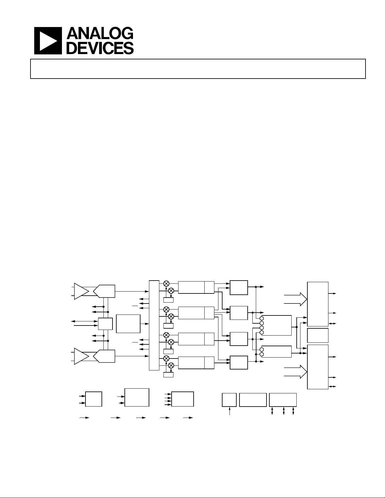
FUNCTIONAL BLOCK DIAGRAM
DUAL-CHANNEL 12-BIT A/D FRONT END WIDEBAND DIGITAL DOWNCONVERTER (DDC)
INA
SHA
–
REF
ENSE
INB+
SHA
INB–
PDWN
SHRDREF
+3.0AVDD +3.3VDDIO 2.5VDD AGND DGND
REFTA
REFBA
REFTB
REFBB
MODE
SELECT
CHANNEL
CHANNEL
ADC
A
VREF
ADC
B
ACLK
DUTYEN
12
CHANNEL A
/
OTRA
LIA
LIA
PSEUDO
RANDOM
NOISE
SEQUENCE
LIB
LIB
OTRB
12
/
CHANNEL B
CLOCK
DUTY
CYCLE
STABILIZER
INPUT MATRIX
SYNCA
SYNCB
SYNCC
SYNCD
NCO
NCO
NCO
NCO
RCIC2
RESAMPLER
RCIC2
RESAMPLER
RCIC2
RESAMPLER
RCIC2
RESAMPLER
EXTERNAL
SYNC.
CIRCUIT
IF to Baseband Diversity Receiver
AD6652
APPLICATIONS
Communications
Diversity radio systems
Multimode digital receivers:
GSM, EDGE, PHS, AMPS, UMTS, WCDMA, CDMA-ONE,
IS95, IS136, CDMA2000, IMT-2000
I/Q demodulation systems
Smart antenna systems
General-purpose software radios
Broadband data applications
Instrumentation and test equipment
CIC5
CIC5
CIC5
CIC5
*DATA INTERLEAVING AND INTERPOLATING HB FILTER
RAM
COEF.
FILTER
CHANNEL 0
RAM
COEF.
FILTER
CHANNEL 1
RAM
COEF.
FILTER
CHANNEL 2
RAM
COEF.
FILTER
CHANNEL 3
DDC
CLK
CLK DATA CONT ADD
BUILT-IN
SELF-TEST
CIRCUITRY
TO OUTPUT PORTS
CHANNELS 0, 1, 2, 3
TO OUTPUT PORTS
TO OUTPUT
PORTS
TO OUTPUT PORTS
CHANNELS 0, 1, 2, 3
Figure 1.
RCF OUTPUTS
AGC A*
AGC B*
RCF OUTPUTS
PROGRAM
MICROPORT
/
/
833
PORT A
8-BIT DSP
LINK
OR
16-BIT
PARALLEL
OUTPUT
CONTROL
OUTPUT
MUX
CIRCUITRY
PORT B
8-BIT DSP
LINK
OR
16-BIT
PARALLEL
OUTPUT
CONTROL
/
03198-0-001
Rev. 0
Information furnished by Analog Devices is believed to be accurate and reliable.
However, no responsibility is assumed by Analog Devices for its use, nor for any
infringements of patents or other rights of third parties that may result from its use.
Specifications subject to change without notice. No license is granted by implication
or otherwise under any patent or patent rights of Analog Devices. Trademarks and
registered trademarks are the property of their respective owners.
One Technology Way, P.O. Box 9106, Norwood, MA 02062-9106, U.S.A.
Tel: 781.329.4700
Fax: 781.326.8703 © 2004 Analog Devices, Inc. All rights reserved.
www.analog.com

AD6652
TABLE OF CONTENTS
Product Description......................................................................... 4
Gain Switching............................................................................ 31
Product Highlights....................................................................... 4
Specifications..................................................................................... 5
Recommended Operating Conditions ...................................... 5
ADC DC Specifications ............................................................... 5
ADC Switching Specifications.................................................... 5
ADC AC Specifications ............................................................... 6
Electrical Characteristics ............................................................. 7
General Timing Characteristics ................................................. 8
Microprocessor Port Timing Characteristics ........................... 9
Absolute Maximum Ratings.......................................................... 10
Thermal Characteristics ............................................................10
Test Level .....................................................................................10
ESD Caution................................................................................ 10
Pin Configuration and Function Descriptions........................... 11
Typical Performance Characteristics ...........................................14
Numerically Controlled Oscillator............................................... 33
Frequency Translation to Baseband......................................... 33
NCO Shadow Register............................................................... 33
NCO Frequency Hold-Off Register......................................... 33
Phase Offset................................................................................. 33
NCO Control Register............................................................... 33
Second-Order rCIC Filter ............................................................. 35
rCIC2 Scale Factor ..................................................................... 35
rCIC2 Output Level ................................................................... 36
rCIC2 Rejection.......................................................................... 36
Decimation and Interpolation Registers ................................. 36
rCIC2 Scale Register .................................................................. 36
Fifth-Order CIC Filter ................................................................... 37
CIC5 Rejection ........................................................................... 37
RAM Coefficient Filter .................................................................. 38
DDC Timing Diagrams .................................................................17
Terminology ....................................................................................23
ADC Equivalent Circuits........................................................... 23
Theory of Operation ...................................................................... 24
ADC Architecture ...................................................................... 24
Digital Downconverter Architecture Overview .........................29
Data Input Matrix....................................................................... 29
Numerically Controlled Oscillator...........................................29
Second-Order rCIC Filter .........................................................29
Fifth-Order CIC Filter ............................................................... 29
RAM Coefficient Filter ..............................................................29
Interpolating Half-Band Filters and AGC............................... 29
Control Register and Memory Map Address Notation .............31
DDC Input Matrix...................................................................... 31
DDC Data Latency ..................................................................... 31
RCF Decimation Register.......................................................... 38
RCF Decimation Phase.............................................................. 38
RCF Filter Length....................................................................... 38
RCF Output Scale Factor and Control Register..................... 39
Interpolating Half-Band Filters .................................................... 40
Automatic Gain Control................................................................ 41
AGC Loop ................................................................................... 41
Desired Signal Level Mode........................................................ 41
Synchronization.......................................................................... 44
User-Configurable Built-In Self-Test (BIST).............................. 45
RAM BIST................................................................................... 45
Channel BIST.............................................................................. 45
Channel/Chip Synchronization.................................................... 46
Start .............................................................................................. 46
Hop............................................................................................... 48
Rev. 0 | Page 2 of 76

AD6652
Parallel Output Ports.......................................................................50
Pin_Sync Control Register.........................................................57
Channel Mode .............................................................................50
AGC Mode...................................................................................51
Master/Slave PCLK Modes........................................................52
Parallel Port Pin Functions ........................................................52
Link Port...........................................................................................53
Link Port Data Format ...............................................................53
Link Port Timing.........................................................................53
TigerSHARC Configuration......................................................54
External Memory Map ...................................................................55
Access Control Register (ACR).................................................56
Channel Address Register (CAR) .............................................56
Soft_Sync Control Register........................................................56
REVISION HISTORY
7/04—Revision 0: Initial Version
Sleep Control Register................................................................57
Data Address Registers...............................................................57
Channel Address Registers (CAR)............................................57
Input Port Control Registers .....................................................63
Output Port Control Registers ..................................................64
Microport Control......................................................................71
Applications .....................................................................................73
AD6652 Receiver Applications..................................................73
Design Guidelines.......................................................................73
AD6652 Evaluation Board and Software.....................................75
Outline Dimensions........................................................................76
Ordering Guide ...........................................................................76
Rev. 0 | Page 3 of 76

AD6652
PRODUCT DESCRIPTION
The AD6652 is a mixed-signal IF to baseband receiver
consisting of dual 12-bit 65 MSPS ADCs and a wideband
multimode digital downconverter (DDC). The AD6652 is
designed to support communications applications where low
cost, small size, and versatility are desired. The AD6652 is also
suitable for other applications in imaging, medical ultrasound,
instrumentation, and test equipment.
The dual ADC core features a multistage differential pipelined
architecture with integrated output error correction logic. Both
ADCs feature wide bandwidth differential sample-and-hold
analog input amplifiers supporting a variety of user-selectable
input ranges. An integrated voltage reference eases design
considerations. A duty cycle stabilizer is provided to compensate for variations in the ADC clock duty cycle, allowing the
converters to maintain excellent performance.
ADC data outputs are internally connected directly to the
receiver’s digital downconverter (DDC) input matrix, simplifying layout and reducing interconnection parasitics. Overrange
bits are provided for each ADC channel to alert the user to
ADC clipping. Level indicator bits are also provided for each
DDC input port that can be used for external digital VGA
control.
The digital receiver has four reconfigurable channels and
provides extraordinary processing flexibility. The receiver input
matrix routes the ADC data to individual channels, or to all four
receive processing channels. Each receive channel has five
cascaded signal processing stages: a 32-bit frequency translator
(numerically controlled oscillator (NCO)), two fixed-coefficient
decimating filters (CIC), a programmable RAM coefficient
decimating FIR filter (RCF), and an interpolating half-band
filter/AGC stage. Following the CIC filters, one, several, or all
channels can be configured to use one, several, or all the RCF
filters. This permits the processing power of four 160-tap RCF
FIR filters to be combined or used individually.
After FIR filtering, data can be routed directly to the two
external 16-bit output ports. Alternatively, data can be routed
through two additional half-band interpolation stages, where up
to four channels can be combined (interleaved), interpolated,
and processed by an automatic gain control (AGC) circuit with
96 dB range. The outputs from the two AGC stages are also
routed directly to the two external 16-bit output ports. Each
output port has a 16-bit parallel output and an 8-bit link port to
permit seamless data interface with DSP devices such as the
TS-101 TigerSHARC® DSP. A multiplexer for each port selects
one of six data sources to appear on the device outputs pins.
digitizes a wide spectrum of IF frequencies and then downconverts the desired signals to baseband using individual
channel NCOs. The AD6652 provides user-configurable digital
filters for removal of undesired baseband components, and the
data is then passed on to an external DSP, where demodulation
and other signal processing tasks are performed to complete the
information retrieval process. Each receive channel is independently configurable to provide simultaneous reception of the
carrier to which it is tuned. This IF sampling architecture
greatly reduces component cost and complexity compared with
traditional analog techniques or less integrated digital methods.
High dynamic range decimation filters offer a wide range of
decimation rates. The RAM-based architecture allows easy
reconfiguration for multimode applications. The decimating
filters remove unwanted signals and noise from the channel of
interest. When the channel occupies less bandwidth than the
input signal, this rejection of out-of-band noise is referred to as
processing gain. By using large decimation factors, this processing gain can improve the SNR of the ADC by 20 dB or more. In
addition, the programmable RAM coefficient filter allows
antialiasing, matched filtering, and static equalization functions
to be combined in a single, cost-effective filter.
Flexible power-down options allow significant power savings,
when desired.
PRODUCT HIGHLIGHTS
• Integrated dual 12-bit 65 MSPS ADC.
• Integrated wideband digital downconverter (DDC).
• Proprietary, differential SHA input maintains excellent
SNR performance for input frequencies up to 200 MHz.
• Crossbar-switched digital downconverter input ports.
• Digital resampling permits noninteger relationships
between the ADC clock and the digital output data rate.
• Energy-saving power-down modes.
• 32-bit NCOs with selectable amplitude and phase dithering
for better than −100 dBc spurious performance.
• CIC filters with user-programmable decimation and
interpolation factors.
• 160-tap RAM coefficient filter for each DDC channel.
• Dual 16-bit parallel output ports and dual 8-bit link ports.
The AD6652 is part of the Analog Devices SoftCell® multimode
and multicarrier transceiver chipset. The SoftCell receiver
Rev. 0 | Page 4 of 76
• 8-bit microport for register programming, register read-
back, and coefficient memory programming.
AD6652
SPECIFICATIONS
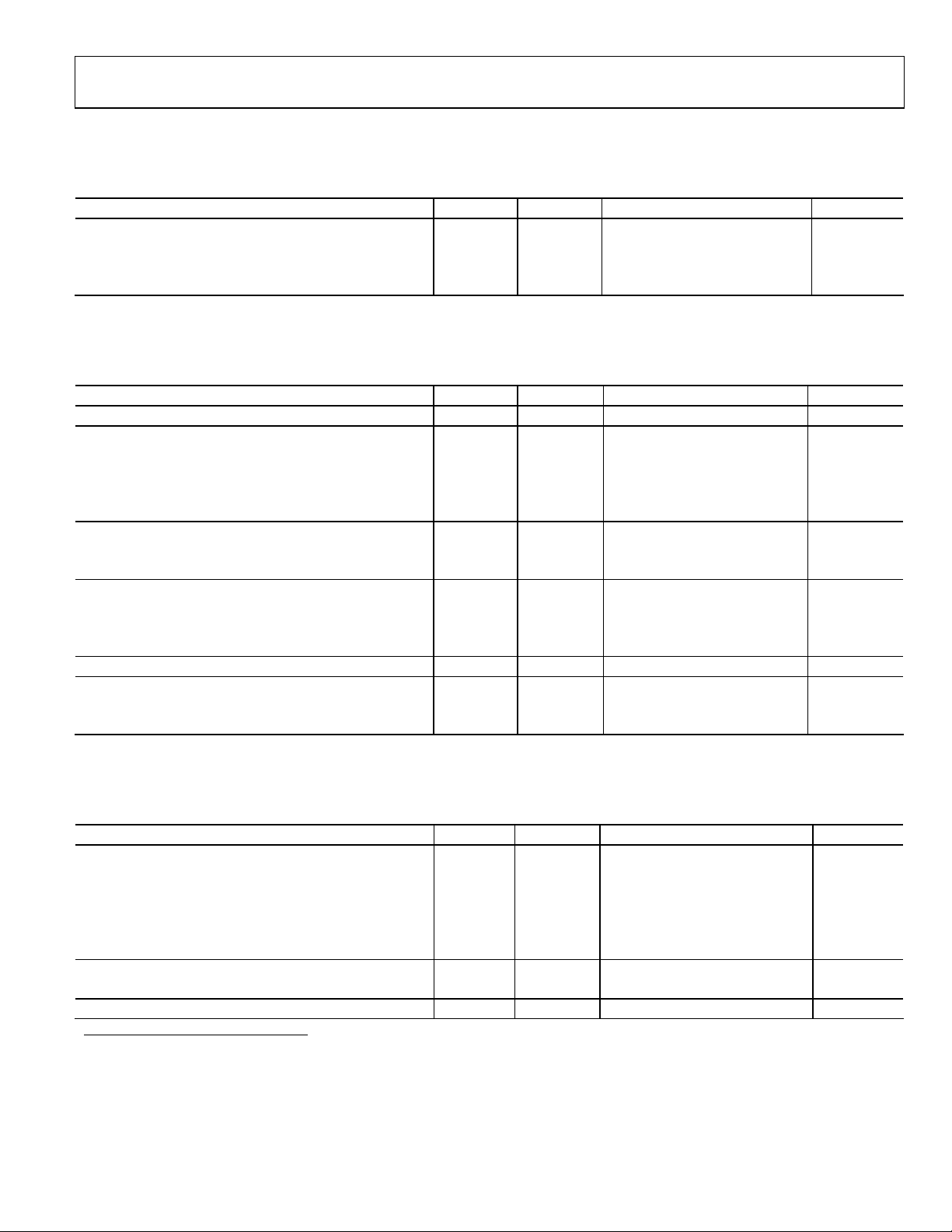
RECOMMENDED OPERATING CONDITIONS
Table 1.
Parameter Temp Test Level Min Typ Max Unit
AVDD Full IV 2.75 3.0 3.3 V
VDD Full IV 2.25 2.5 2.75 V
VDDIO Full IV 3.0 3.3 3.6 V
T
AMBIENT
ADC DC SPECIFICATIONS
AVDD = 3.0 V, VDD = 2.5 V, VDDIO = 3.3 V, 61.44 MSPS, −1.0 dBFS differential input, 1.0 V internal reference, unless otherwise noted.
Table 2.
Parameter (Conditions) Temp Test Level Min Typ Max Unit
RESOLUTION Full IV 12 Bits
INTERNAL VOLTAGE REFERENCE
Output Voltage Error (1 V Mode) Full IV ±5 ±35 mV
Load Regulation @ 1.0 mA Full V 0.8 mV
Output Voltage Error (0.5 V Mode) Full V ±2.5 mV
Load Regulation @ 0.5 mA Full V 0.1 mV
INPUT REFERRED NOISE
Input Span = 1 V Internal 25°C V 0.54 LSB rms
Input Span = 2 V Internal 25°C V 0.27 LSB rms
ANALOG INPUT
Input Span = 1.0 V Full IV 1 V p-p
Input Span = 2.0 V Full IV 2 V p-p
Input Capacitance Full V 7 pF
REFERENCE INPUT RESISTANCE Full V 7 kΩ
MATCHING CHARACTERISTICS
Offset Error Full V ±0.1 % FSR
Gain Error Full V ±0.1 % FSR
IV −40 +25 +85 °C
ADC SWITCHING SPECIFICATIONS
AVDD = 3.0 V, VDD = 2.5 V, VDDIO = 3.3 V, 61.44 MSPS, −1.0 dBFS differential input, 1.0 V internal reference, unless otherwise noted.
Table 3.
Parameter (Conditions) Temp Test Level Min Typ Max Unit
SWITCHING PERFORMANCE
Maximum Conversion Rate Full IV 65 MSPS
Minimum Conversion Rate Full V 1 MSPS
ACLK Period Full V 15.4 ns
ACLK Pulse Width High
ACLK Pulse Width Low1 Full V 6.2 ACLK/2 ns
DATA OUTPUT PARAMETERS
Wake-Up Time
2
OUT-OF-RANGE RECOVERY TIME Full V 2 Cycles
1
Duty cycle stabilizer enabled.
2
Wake-up time is dependent on the value of decoupling capacitors, typical values shown with 0.1 µF and 10 µF capacitors on REFT and REFB.
1
Full V 6.2 ACLK/2 ns
Full V 2.5 ms
Rev. 0 | Page 5 of 76

AD6652
ADC AC SPECIFICATIONS
AVDD = 3.0 V, VDD = 2.5 V, VDDIO = 3.3 V, 61.44 MSPS, −1.0 dBFS differential input, 1.0 V internal reference.
Table 4.
Parameter (Conditions) Temp Test Level Min Typ Max Unit
SIGNAL-TO-NOISE RATIO1 (WITHOUT HARMONICS)
Analog Input Frequency 10.4 MHz 25°C V 90 dB
Full V 90 dB
25.0 MHz 25°C II 85 90 dB
Full V 90 dB
68.0 MHz 25°C II 84 89.5 dB
Full V 88.5 dB
101 MHz 25°C V 88.0 dB
150 MHz 25°C V 87.5 dB
200 MHz 25°C V 85 dB
WORST HARMONIC (2nd or 3rd)1
Analog Input Frequency 10.4 MHz 25°C V −85 dBc
Full V −83 dBc
25 MHz 25°C II −83 −71 dBc
Full V −80 dBc
68 MHz 25°C II −80 dBc
Full V −76 dBc
101 MHz 25°C V −79 dBc
150 MHz 25°C V −72 dBc
200 MHz 25°C V −69 dBc
TWO-TONE IMD REJECTION (TWO TONES SEPARATED BY 1 MHz)2
Analog Inputs = 15/16 MHz 25°C V −81 dBc
Analog Inputs = 55/56 MHz 25°C V −79 dBc
CHANNEL ISOLATION/CROSSTALK
1
Analog Input A or B = single tone @ −1 dB below full scale, 150 kHz DDC filter bandwidth.
2
Analog Input A or B = each single tone @ −7 dB below full scale, 5 MHz DDC filter bandwidth.
3
Analog Inputs A and B = each single tone @ −1 dB below full scale at 4.3 MHz and 68 MHz, 150 kHz DDC filter bandwidth.
3
Full V 85 dB
Rev. 0 | Page 6 of 76

AD6652
ELECTRICAL CHARACTERISTICS
AVDD = 3.0 V, VDD = 2.5 V, VDDIO = 3.3 V, 61.44 MSPS, −1.0 dBFS differential input, 1.0 V internal reference, unless otherwise noted.
Table 5.
Parameter (Conditions) Temp Test Level Min Typ Max Unit
LOGIC INPUTS
Logic Compatibility Full IV 3.3 V CMOS
Logic 1 Voltage Full IV 2.0 V
Logic 0 Voltage Full IV 0.8 V
Logic 1 Current Full IV −10 +10 µA
Logic 0 Current Full IV −10 +10 µA
Input Capacitance 25°C V 4 pF
LOGIC OUTPUTS
Logic Compatibility Full IV 3.3 V CMOS/TTL
Logic 1 Voltage (VOH) (IOH = 0.25 mA) Full IV 2.4 VDDIO − 0.2 V
Logic 0 Voltage (VOL) (IOL = 0.25 mA) Full IV 0.2 0.4 V
SUPPLY CURRENTS
Narrow Band (150 kHz BW) (61.44 MHz CLK)
Four Individual Channels
I
AVDD
I
VDD
I
VDDIO
CDMA (1.25MHz BW) (61.44 MHz CLK) Example
I
AVDD
I
VDD
I
VDDIO
1
WCDMA (5 MHz BW) (61.44 MHz CLK) Example1
I
AVDD
I
VDD
I
VDDIO
TOTAL POWER DISSIPATION
Narrow Band (150 kHz BW) (61.44 MHz CLK)
Four Individual Channels
CDMA (61.44 MHz)1
WCDMA (61.44 MHz)1
ADC in Standby and DDC in Sleep Mode
2
25°C II 160 200 215 mA
25°C II 240 280 300 mA
25°C II 25 40 45 mA
25°C V 200 mA
25°C V 336 mA
25°C V 68 mA
25°C V 200 mA
25°C V 330 mA
25°C V 89 mA
25°C II 1.2 1.5 1.6 W
25°C
25°C
25°C
V 1.7 W
V 1.7 W
V 2.3 mW
1
All signal processing stages and all DDC channels active.
2
ADC standby power measured with ACLK inactive.
Rev. 0 | Page 7 of 76
AD6652
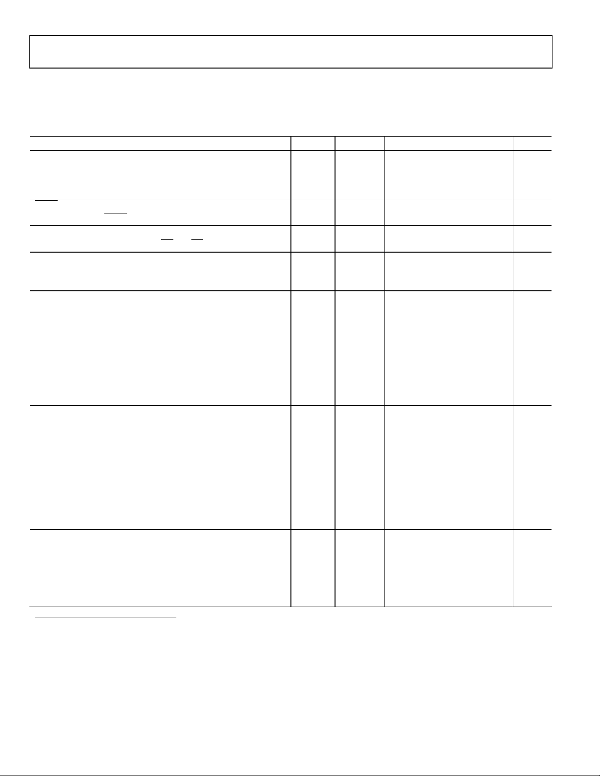
GENERAL TIMING CHARACTERISTICS
All timing specifications valid over VDD range of 2.25 V to 2.75 V and VDDIO range of 3.0 V to 3.6 V.
CLOAD = 40 pF on all outputs, unless otherwise specified.
Table 6.
Parameter (Conditions) Temp Test Level Min Typ Max Unit
CLK TIMING REQUIREMENTS
t
CLK
t
CLKL
t
CLKH
RESET TIMING REQUIREMENTS
t
RESL
LEVEL INDICATOR OUTPUT SWITCHING CHARACTERISTICS
t
DLI
SYNC TIMING REQUIREMENTS
t
SS
t
HS
PARALLEL PORT TIMING REQUIREMENTS (MASTER MODE)
Switching Characteristics
t
DPOCLKL
t
DPOCLKLL
t
DPREQ
t
DPP
Input Characteristics
t
SPA
t
HPA
PARALLEL PORT TIMING REQUIREMENTS (SLAVE MODE)
Switching Characteristics1
t
POCLK
t
POCLKL
t
POCLKH
t
DPREQ
t
DPP
Input Characteristics
t
SPA
t
HPA
LINK PORT TIMING REQUIREMENTS
Switching Characteristics1
t
RDLCLK
t
FDLCLK
t
RLCLKDAT
t
FLCLKDAT
1
The timing parameters for Px[15:0], PxREQ, and PxACK apply for Port A and B (x stands for A or B).
CLK Period Full IV 15.4 ns
CLK Width Low Full IV 6.2 t
CLK Width High Full IV 6.2 t
/2 ns
CLK
/2 ns
CLK
RESET Width Low
↑CLK to LI (LIA, LIA; LIB, LIB) Output Delay Time
SYNC(A,B,C,D) to ↑CLK Setup Time
SYNC(A,B,C,D) to ↑CLK Hold Time
1
↓CLK to ↑PCLK Delay (Divide-by-1)
↓CLK to ↑PCLK Delay (Divide-by-2, -4, or -8)
↑PCLK to ↑PxREQ Delay
↑PCLK to Px[15:0] Delay
PxACK to ↓PCLK Setup Time
PxACK to ↓PCLK Hold Time
Full IV 30.0 ns
Full IV 3.3 10.0 ns
Full IV 2.0 ns
Full IV 1.0 ns
Full IV 6.5 10.5 ns
Full IV 8.3 14.6 ns
1.0 ns
0.0 ns
7.0 ns
−3.0 ns
PCLK Period Full IV 12.5 ns
PCLK Low Period (when PCLK Divisor = 1) Full IV 2.0 0.5 × t
PCLK High Period (when PCLK Divisor = 1) Full IV 2.0 0.5 × t
↑PCLK to ↑PxREQ Delay
↑PCLK to Px[15:0] Delay
PxACK to ↓PCLK Setup Time
PxACK to ↓PCLK Hold Time
10.0 ns
11.0 ns
IV 1.0 ns
IV 1.0 ns
↑PCLK to ↑LxCLKOUT Delay
↓PCLK to ↓LxCLKOUT Delay
↑LCLKOUT to Lx[7:0] Delay
↓LCLKOUT to Lx[7:0] Delay
Full IV 2.5 ns
Full IV 0 ns
Full IV 0 2.9 ns
Full IV 0 2.2 ns
POCLK
POCLK
ns
ns
Rev. 0 | Page 8 of 76
AD6652
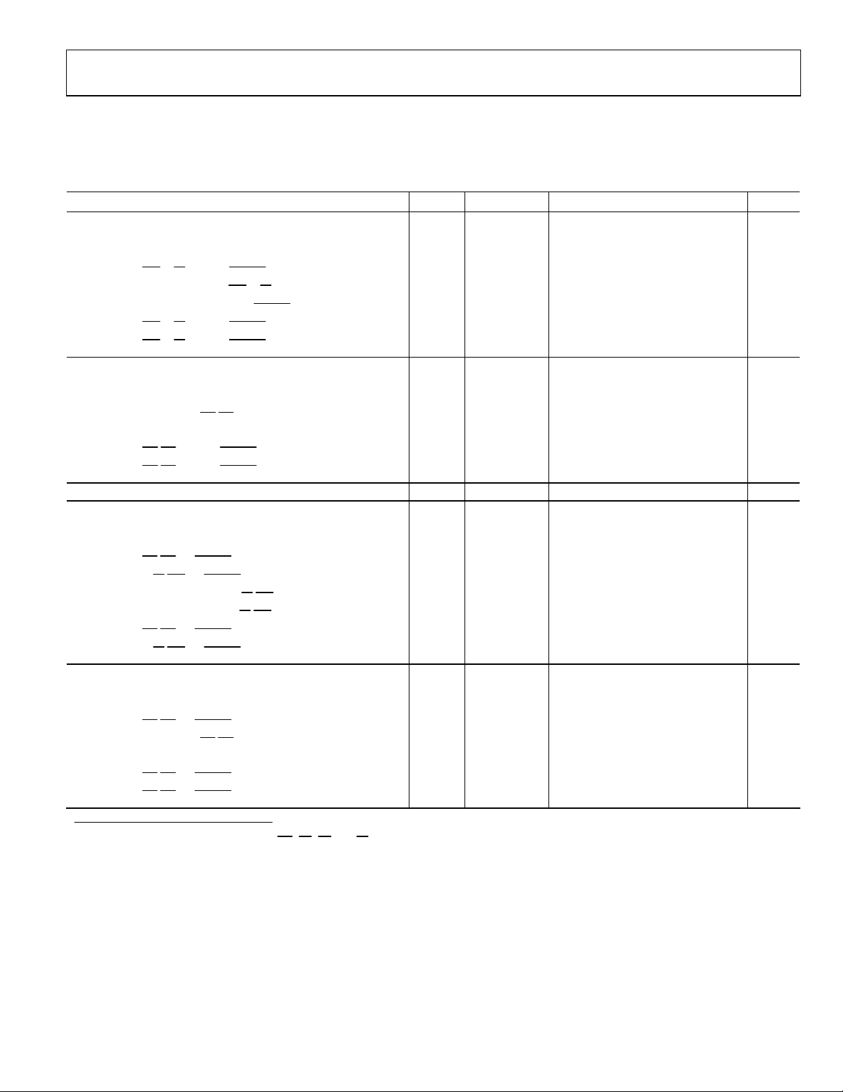
MICROPROCESSOR PORT TIMING CHARACTERISTICS
All timing specifications valid over VDD range of 2.25 V to 2.75 V and VDDIO range of 3.0 V to 3.6 V.
CLOAD = 40 pF on all outputs, unless otherwise specified.
Table 7.
MICROPROCESSOR PORT, MODE INM (MODE = 0) Temp Test Level Min Typ Max Unit
MODE INM WRITE TIMING
t
t
t
t
t
t
t
SC
HC
HWR
SAM
HAM
DRDY
ACC
Control1 to ↑CLK Setup Time
Control1 to ↑CLK Hold Time
WR(R/W) to RDY(DTACK) Hold Time
Address/Data to WR(R/W) Setup Time
Address/Data to RDY(DTACK) Hold Time
WR(R/W) to RDY(DTACK) Delay
WR(R/W) to RDY(DTACK) High Delay
MODE INM READ TIMING
t
t
t
t
t
t
SC
HC
SAM
HAM
DRDY
ACC
Control1 to ↑CLK Setup Time
Control1 to ↑CLK Hold Time
Address to RD(DS) Setup Time
Address to Data Hold Time Full IV 5.0 ns
RD(DS) to RDY(DTACK) Delay
RD(DS) to RDY(DTACK) High Delay
MICROPROCESSOR PORT, MODE MNM (MODE = 1) Temp Test Level Min Typ Max Unit
MODE MNM WRITE TIMING
t
SC
t
HC
t
HDS
t
HRW
t
SAM
t
HAM
t
DDTACK
t
ACC
Control1 to ↑CLK Setup Time
Control1 to ↑CLK Hold Time
DS(RD) to DTACK(RDY) Hold Time
R/W(WR) to DTACK(RDY) Hold Time
Address/Data To R/W(WR) Setup Time
Address/Data to R/W(WR) Hold Time
DS(RD) to DTACK(RDY) Delay
R/W(WR) to DTACK(RDY) Low Delay
MODE MNM READ TIMING
t
SC
t
HC
t
HDS
t
SAM
t
HAM
t
DDTACK
t
ACC
Control1 to ↑CLK Setup Time
Control1 to ↑CLK Hold Time
DS(RD) to DTACK(RDY) Hold Time
Address to DS(RD) Setup Time
Address to Data Hold Time Full IV 5.0 ns
DS(RD) to DTACK(RDY) Delay
DS(RD) to DTACK(RDY) Low Delay
Full IV 2.0 ns
Full IV 2.5 ns
Full IV 7.0 ns
Full IV 3.0 ns
Full IV 5.0 ns
Full IV 8.0 ns
Full IV 4 × t
CLK
5 × t
CLK
9 × t
CLK
ns
Full IV 5.0 ns
Full IV 2.0 ns
Full IV 0.0 ns
Full IV 8.0 ns
Full IV 8 × t
CLK
10 × t
CLK
13 × t
CLK
ns
Full IV 2.0 ns
Full IV 2.5 ns
Full IV 8.0 ns
Full IV 7.0 ns
Full IV 3.0 ns
Full IV 5.0 ns
Full IV 8.0 ns
Full IV 4 × t
CLK
5 × t
CLK
9 × t
CLK
ns
Full IV 5.0 ns
Full IV 2.0 ns
Full IV 8.0 ns
Full IV 0.0 ns
Full IV 8.0 ns
Full IV 8 × t
CLK
10 × t
CLK
13 × t
CLK
ns
1
Specification pertains to control signals: R/W, (WR), DS, (RD), and CS.
Rev. 0 | Page 9 of 76

AD6652
ABSOLUTE MAXIMUM RATINGS
Table 8.
Parameter Rating
ELECTRICAL
AVDD Voltage −0.3 V to +3.9 V
VDD Voltage −0.3 V to +2.75 V
VDDIO Voltage −0.3 V to +3.9 V
AGND, DGND −0.3 V to +0.3 V
ADC VINA, VINB Analog Input Voltage −0.3 V to AVDD + 0.3 V
ADC Digital Input Voltage −0.3 V to AVDD + 0.3 V
ADC OTRA, OTRB Digital Output Voltage
ADC VREF, REFA, REFB Input Voltage −0.3 V to AVDD + 0.3 V
DDC Digital Input Voltage −0.3 V to VDDIO + 0.3 V
DDC Digital Output Voltage −0.3 V to VDDIO + 0.3 V
ENVIRONMENTAL
Operating Temperature Range
(Ambient)
Maximum Junction Temperature
Under Bias
Storage Temperature Range (Ambient) −65°C to +150°C
−0.3 V to VDDIO + 0.3 V
−40°C to +85°C
150°C
Stresses above those listed under the Absolute Maximum
Ratings may cause permanent damage to the device. This is a
stress rating only; functional operation of the device at these or
any other conditions above those indicated in the operational
section of this specification is not implied. Exposure to absolute
maximum rating conditions for extended periods may affect
device reliability.
THERMAL CHARACTERISTICS
256-lead CSPBGA, 17 mm sq.
= 23°C/W, still air.
θ
JA
Estimate based on JEDEC JC51-2 model using horizontally
positioned 4-layer board.
TEST LEVEL
I. 100% production tested.
II.
100% production tested at 25°C.
III. Sample tested only.
IV. Parameter guaranteed by design and characterization testing.
V. Parameter is a typical value only.
VI.
100% production tested at 25°C; guaranteed by design and
characterization testing for industrial temperature range.
ESD CAUTION
ESD (electrostatic discharge) sensitive device. Electrostatic charges as high as 4000 V readily accumulate on
the human body and test equipment and can discharge without detection. Although this product features
proprietary ESD protection circuitry, permanent damage may occur on devices subjected to high energy
electrostatic discharges. Therefore, proper ESD precautions are recommended to avoid performance
degradation or loss of functionality.
Rev. 0 | Page 10 of 76
AD6652
PIN CONFIGURATION AND FUNCTION DESCRIPTIONS
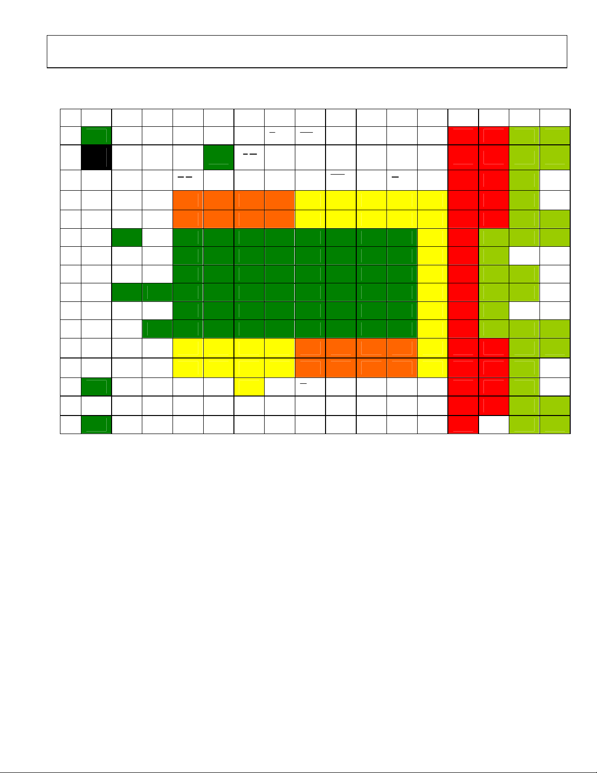
Table 9. BGA Pin Configuration (Top View)
1 2 3 4 5 6 7 8 9 10 11 12 13 14 15 16
DGND PA7_LA7 A2 PA6_LA6 D1 D3
A
Do Not
Connect
PA4_LA4
B
PA9 PA3_LA3 A1
C
PA1_LA1 PA2_LA2
D
PA8 PA5_LA5 n.c. VDD VDD VDD VDD VDDIO VDDIO VDDIO VDDIO VDDIO AVDD AVDD AGND AGND
E
PA0_LA0 DGND PA10 DGND DGND DGND DGND DGND DGND DGND DGND VDDIO AVDD AGND AGND AGND
F
PA12 PA11 PA13 DGND DGND DGND DGND DGND DGND DGND DGND VDDIO AVDD AGND REFBB REFTB
G
PAR EQ PA 15 PA1 4 DGND DGND DGND DGND DGND DGND DGND DGND VDDIO AVDD AGND AGND SENSE
H
CHIP_ID1 DGND DGND DGND DGND DGND DGND DGND DGND DGND DGND VDDIO AVDD AGND AGND VREF
J
CHIP_ID3 PAACK CHIP_ID0 DGND DGND DGND DGND DGND DGND DGND DGND VDDIO AVDD AGND REFBA REFTA
K
PB6_LB6 PB7_LB7 DGND DGND DGND DGND DGND DGND DGND DGND DGND VDDIO AVDD AGND AGND AGND
L
PAC H0 _
LACLK
OUT
PAC H1 _
LACLKIN
A0
DS (RD
VDD VDD VDD VDD VDDIO VDDIO VDDIO VDDIO VDDIO AVDD AVDD AGND VI N−B
DGND
D0 D2 D5 D7
)
R/
CS RESE T
W (WR
D4 D6 SYNCC SYNCA LIA DUTYEN
)
MODE SYNCD OTRA PDWN AVDD AVDD AGND AGND
DTACK
(RDY)
SYNCB
LIA
AVDD AVDD AGND AGND
LIB AVDD AVDD AGND VIN+B
CHIP_ID2 PB3_LB3 PB4_LB4 VDDIO VDDIO VDDIO VDDIO VDD VDD VDD VDD VDDIO AVDD AVDD AG ND AGND
M
PAI Q
N
P
PBIQ
R
DGND PCLK PB5_ LB5 PB11 PB13 PBREQ n.c. n.c. n.c. n.c. DCLK SHRDREF AVDD ACLK AGND AGND
T
PBCH1_
LBCLK IN
DGND PB0_LB0 PB8 PB10 PB14 VDDIO PBACK
PBCH0_L
BCLKOUT
PB2_LB2
PB1_ LB1 PB9 PB12 PB15 n.c. n.c. n.c. n.c. n.c. PDWN
VDDIO VDDIO VDDIO VDDIO VDD VDD VDD VDD VDDIO AVDD AVDD AGND VI N−A
LIB
n.c. n.c. OTRB n.c. AVDD AVDD AGN D VIN+A
AVDD AVDD AGND AGND
Rev. 0 | Page 11 of 76
AD6652
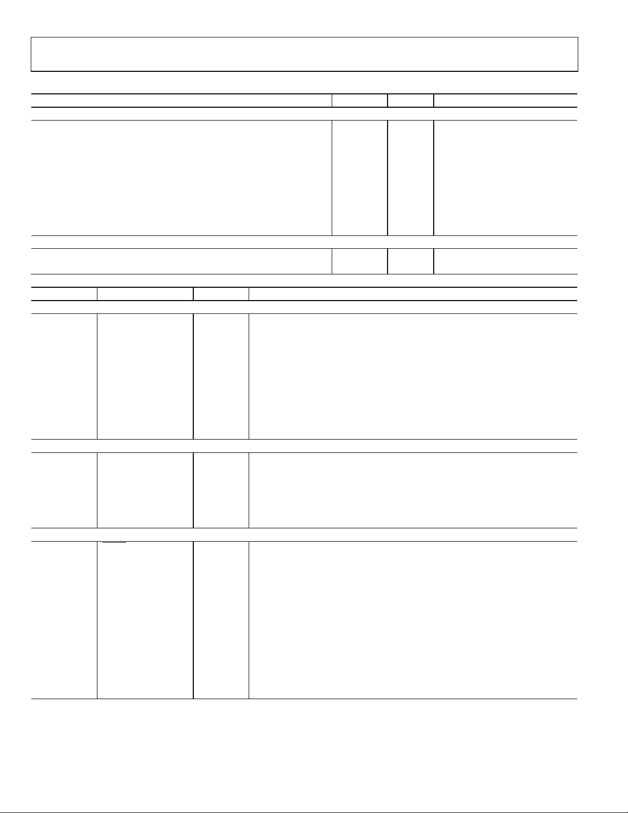
Table 10. Pin Function Descriptions
Pin No. Mnemonic Type Function
POWER SUPPLY
A13, B13, C13, D13, E13, F13, G13, H13, J13, K13, L13, M13, N13, P13, R13,
T13, A14, B14, C14, D14, E14, M14, N14, P14, R14
D4, D5, D6, D7, E4, E5, E6, E7, M8, M9, M10, M11, N8, N9, N10, N11 VDD Power 2.5 V Digital Core Supply, 16 Pins.
D8, D9, D10, D11, D12, E8, E9, E10, E11, E12, F12, G12, H12, J12, K12, L12,
M4, M5, M6, M7, M12, N4, N5, N6, N7, N12, P6
A1, B5, F2, F4, F5, F6, F7, F8, F9, F10, F11, G4, G5, G6, G7, G8, G9, G10, G11,
H4, H5, H6, H7, H8, H9, H10, H11, J2, J3, J4, J5, J6, J7, J8, J9, J10, J11, K4,
K5, K6, K7, K8, K9, K10, K11, L3, L4, L5, L6, L7, L8, L9, L10, L11, P1, T1
A15, A16, B15, B16, C15, D15, E15, E16, F14, F15, F16, G14, H14, H15, J14,
J15, K14, L14, L15, L16, M15, M16, N15, P15, R15, R16, T15, T16
MISCELLANEOUS
E3, P9, P10, P12, R7, R8, R9, R10, R11, T7, T8, T9, T10 NC N/A No Connect, 13 Pins.
B1 DNC N/A Do Not Connect.
Pin No. Mnemonic Type Function
ADC INPUTS
P16 VIN+A Input Differential Analog Input Pin (+) for Channel A.
N16 VIN−A Input Differential Analog Input Pin (−) for Channel A.
C16 VIN+B Input Differential Analog Input Pin (+) for Channel B.
D16 VIN−B Input Differential Analog Input Pin (−) for Channel B.
J16 VREF I/O Voltage Reference Input/Output.
H16 SENSE Input Voltage Reference Mode Select.
T14 ACLK Input ADC Master Clock.
B12 DUTYEN Input Duty Cycle Stabilizer, Active High.
A12, R12 PDWN
1
Input Power-Down Enable, Active High.
T12 SHRDREF Input Shared Voltage Reference Select, Low = Independent, High = Shared.
ADC OUTPUTS
A11 OTRA Output Out-of-Range Indicator for Channel A, High = Overrange.
P11 OTRB Output Out-of-Range Indicator for Channel B, High = Overrange.
K16 REFTA Output Top Reference Voltage, Channel A.
G16 REFTB Output Top Reference Voltage, Channel B.
K15 REFBA Output Bottom Reference Voltage, Channel A.
G15 REFBB Output Bottom Reference Voltage, Channel B.
DDC INPUTS
A8
RESET
Input Master Reset, Active Low.
T11 DCLK Input DDC Master Clock.
T2 PCLK I/O Link Port Clock Output or Parallel Port Clock Input.
D3 PACH1_LACLKIN
2
I/O
Channel ID Output Bit, MSB, for Parallel Port A, or Link Port A Data Ready Input.
Function depends on logic state of 0x1B:7 of output port control register.
N2 PBCH1_LBCLKIN2 I/O
Channel ID Output Bit, MSB, for Parallel Port B, or Link Port B Data Ready Input.
Function depends on logic state of 0x1D:7 of output port control register.
B10 SYNCA
3
Input Hardware Sync, Pin A, Routed to All Receiver Channels.
C10 SYNCB3 Input Hardware Sync, Pin B, Routed to All Receiver Channels.
B9 SYNCC3 Input Hardware Sync, Pin C, Routed to All Receiver Channels.
A10 SYNCD3 Input Hardware Sync, Pin D, Routed to All Receiver Channels.
3
K3, J1, M1,
K1
CHIP_ID[3:0]
Input
Chip ID Selector, Four Pins, Used in Conjunction with Access Control Register
Bits 5–2.
AVDD Power 3.0 V Analog Supply, 25 Pins.
VDDIO Power 3.3 V Digital I/O Supply, 27 Pins.
DGND Ground Digital Ground, 56 Pins.
AGND Ground Analog Ground, 28 Pins.
Rev. 0 | Page 12 of 76
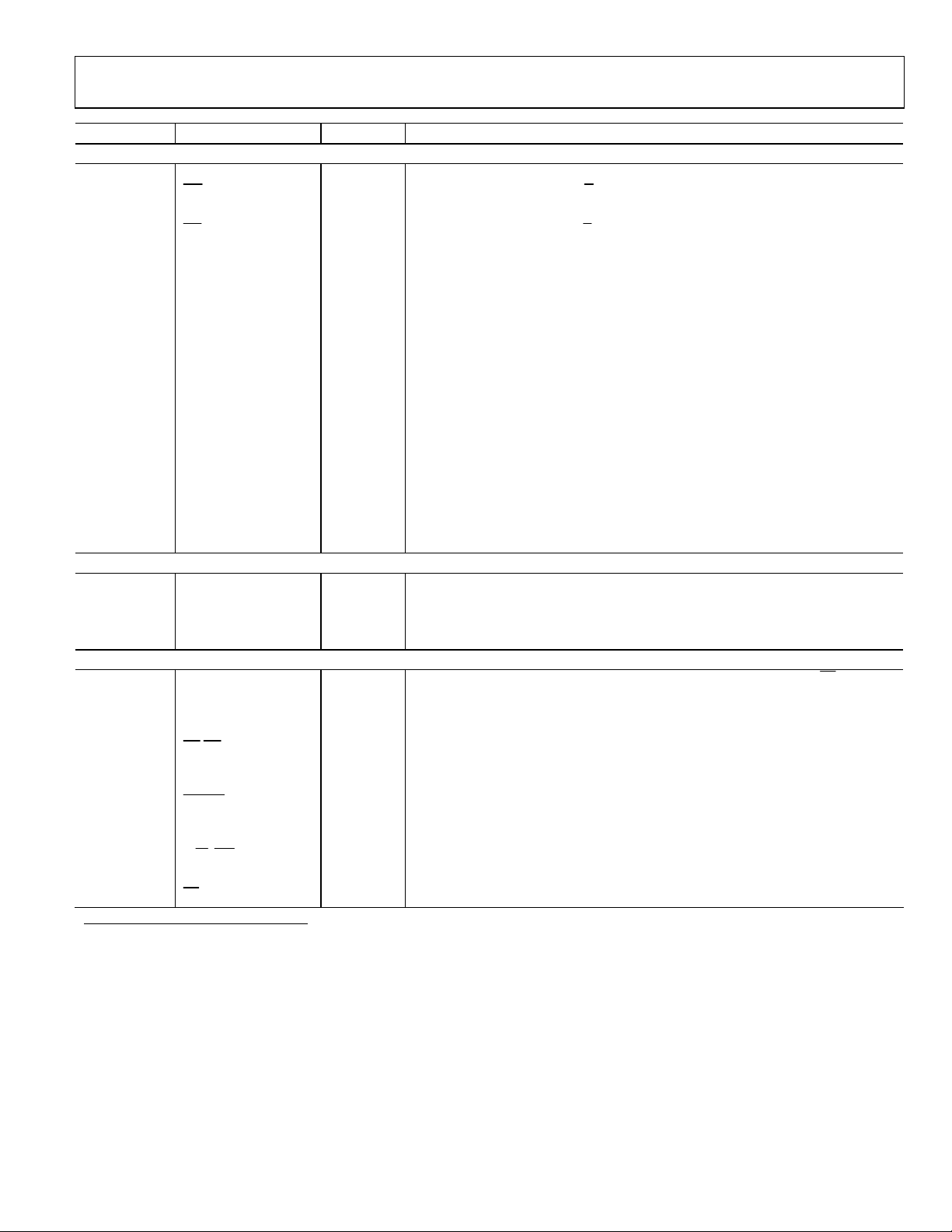
AD6652
Pin No. Mnemonic Type Function
DDC OUTPUTS
B11 LIA Output Level Indicator, Input A, Data A.
C11
LIA
C12 LIB Output Level Indicator, Input B, Data B.
P8
LIB
B3 PACH0_LACLKOUT2 Output
R2 PACH0_LBCLKOUT2 Output
F1, D1, D2,
PA[7:0]_LA[7:0] Output Link Port A Data or Parallel Port A Data [7:0], Eight Pins.
C2, B2, E2,
A4, A2
P2, R3, N3,
PB[7:0_LB[7:0] Output Link Port B Data or Parallel Port B Data [7:0], Eight Pins.
M2, M3, T3,
L1, L2
E1, C1, F3,
PA[15:8] Output Parallel Port A Data [15:8], Eight Pins.
G2, G1, G3,
H3, H2
P3, R4, P4,
PB[15:8] Output Parallel Port B Data [15:8], Eight Pins.
T4, R5, T5,
P5, R6
N1 PAIQ Output Parallel Port A I or Q Data Indicator, I = High, Q = Low.
R1 PBIQ Output Parallel Port B I or Q Data Indicator, I = High, Q = Low.
PARALLEL OUTPUT PORT CONTROL
K2 PAACK Input Parallel Port A Acknowledge.
H1 PAREQ Output Parallel Port A Request.
P7 PBACK Input Parallel Port B Acknowledge.
T6 PBREQ Output Parallel Port B Request.
MICROPORT CONTROL
C5, A5, C6,
D[7:0] I/O
A6, B7, C7,
B8, C8
B4, C3, A3 A[2:0] Input Microport Address Bus, 3 Pins.
C4
C9
B6
4
DS(RD)
DTACK(RDY)
W (WR)4
R/
4, 5
A9 MODE4 Input Mode Select Pin. 0 = Intel mode, 1 = Motorola mode.
A7
CS3
Output
Output
Level Indicator, Input A, Data
Level Indicator, Input B, Data
A.
B.
Channel ID Output Bit, LSB, for Parallel Port A, or Link Port A Clock Output.
Function depends on logic state of 0x1B:7 of output port control register.
Channel ID Output Bit, LSB, for Parallel Port B, or Link Port B Clock Output.
Function depends on logic state of 0x1D:7 of output port control register.
Bidirectional Microport Data, Eight Pins. This bus is three-stated when CS is high.
Input Function depends upon MODE pin.
Active Low Data Strobe when MODE = 1.
Active Low Read Strobe when MODE = 0.
Output Function depends upon MODE pin.
Active Low Data Acknowledge when MODE = 1.
Microport Status Pin when MODE = 0.
Input Read/Write Strobe when MODE = 1. Active Low Write strobe when MODE = 0.
Input Active Low Chip Select. Logic 1 three-states the microport data bus.
1
PDWN pins must be the same logic level: both logic high or both logic low.
2
PACH0 and PACH1 form a 2-bit output word in the parallel output mode that identifies the processing channel (0, 1, 2, or 3) whose data appears on Port A parallel
outputs. Likewise, PBCH0 and PBCH1 identify the channel for Port B.
3
Pins with a pull-down resistor of nominal 70 kΩ.
4
Mode 0 is Intel nonmultiplexed (IMN), and Mode 1 is Motorola nonmultiplexed (MNM). Pin logic level corresponds to mode.
5
Pins with a pull-up resistor of nominal 70 kΩ.
Rev. 0 | Page 13 of 76
AD6652
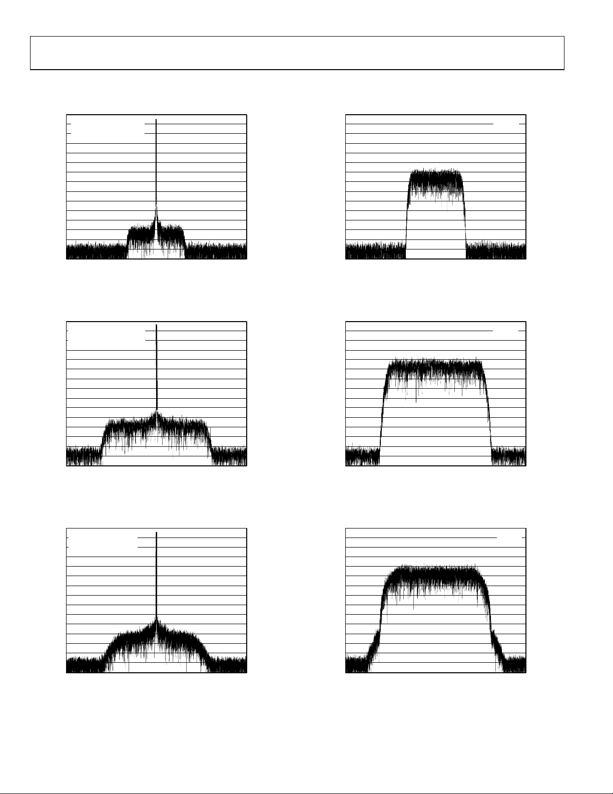
TYPICAL PERFORMANCE CHARACTERISTICS
0
AIN = –1dBFS
–10
SNR = 90dB (200kHz BW)
–20
32k FFT
–30
–40
–50
–60
–70
–80
dBFS
–90
–100
–110
–120
–130
–140
–150
–300 –200 –100 0 100 200 300
FREQUENCY (kHz)
Figure 2. GSM/EDGE with Single Tone A
= 30 MHz; Encode = 61.44 MSPS
IN
0
AIN = –1dBFS
–10
SNR = 80dB (1.25MHz BW)
–20
32k FFT
–30
–40
–50
–60
–70
–80
dBFS
–90
–100
–110
–120
–130
–140
–150
–1.2 –0.8 –0.4 0 0.4 0.8 1.2
FREQUENCY (MHz)
Figure 3. CDMA2000 with Single Tone A
= 76 MHz; Encode = 61.44 MSPS
IN
0
AIN = –1dBFS
–10
SNR = 70dB (5MHz BW)
–20
32k FFT
–30
–40
–
50
–60
–70
–80
dBFS
–90
–100
–110
–120
–130
–140
–150
Figure 4. WCDMA with Single Tone A
–101234–3 –2–4
FREQUENCY (MHz)
= 169 MHz; Encode = 61.44 MSPS
IN
03198-0-060
03198-0-062
03198-0-064
0
–10
–20
–30
–40
–50
–60
–70
–80
dBFS
–90
–100
–110
–120
–130
–140
–150
–300 –200 –100 0 100 200 300
FREQUENCY (kHz)
Figure 5. GSM/EDGE Carrier A
= 30 MHz; Encode = 61.44 MSPS
IN
0
–10
–20
–30
–40
–50
–60
–70
–80
dBFS
–90
–100
–110
–120
–130
–140
–150
–1.2 –0.8 –0.4 0 0.4 0.8 1.2
FREQUENCY (MHz)
Figure 6. CDMA2000 Carrier A
= 76 MHz; Encode = 61.44 MSPS
IN
0
–10
–20
–30
–40
–50
–60
–70
–80
dBFS
–90
–100
–110
–120
–130
–140
–150
Figure 7. WCDMA Carrier A
–101234–3 –2–4
FREQUENCY (MHz)
= 169 MHz; Encode = 61.44 MSPS
IN
32k FFT
32k FFT
32k FFT
03198-0-059
03198-0-061
03198-0-063
Rev. 0 | Page 14 of 76
AD6652
0
ENCODE = 61.44MSPS
–10
A
IN
–20
32k FFT
–30
–40
–50
–60
–70
–80
dBFS
–90
–100
–110
–120
–130
–140
–150
100
= –7dBFS
–101234–3 –2–4
FREQUENCY (MHz)
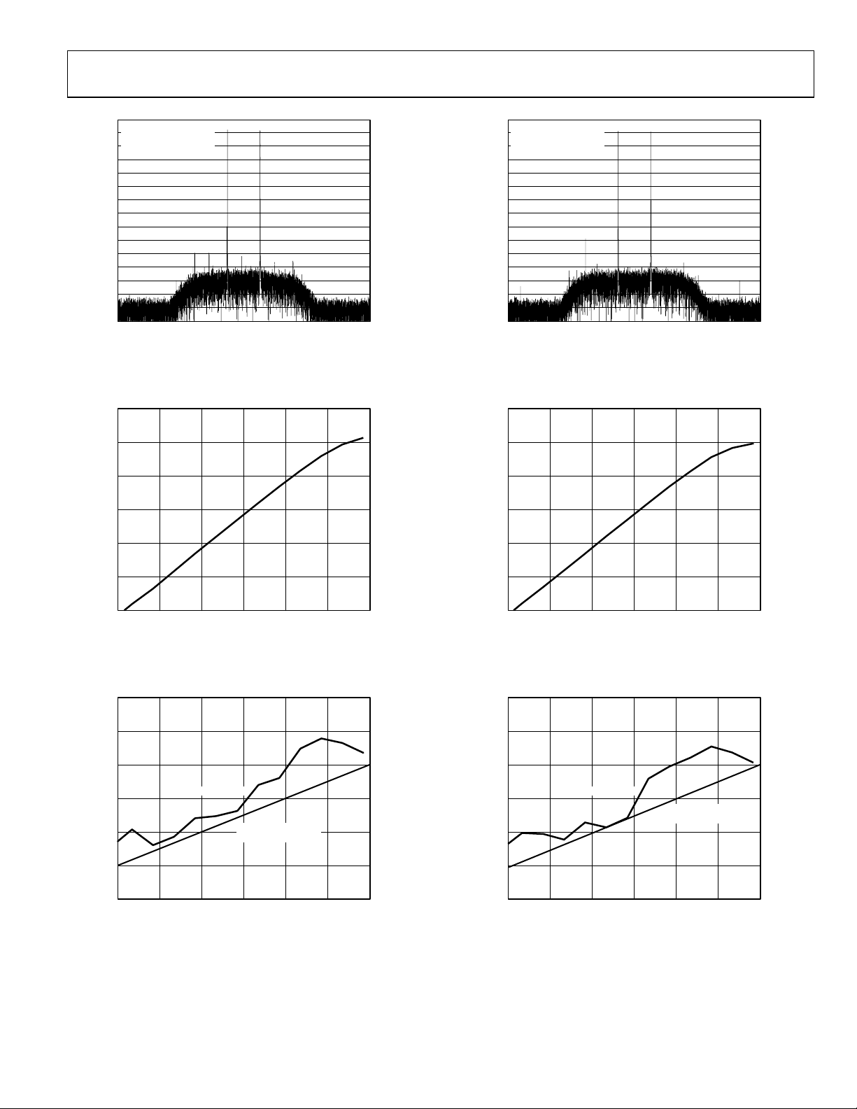
Figure 8. Two Tones at 15 MHz and 16 MHz
03198-0-070
0
ENCODE = 61.44MSPS
–10
A
IN
–20
32k FFT
–30
–40
–50
–60
–70
–80
dBFS
–90
–100
–110
–120
–130
–140
–150
100
= –7dBFS
–101234–3 –2–4
FREQUENCY (MHz)
Fig z ure 11. Two Tones at 55 MHz and 56 MH
03198-0-066
90
80
70
60
SNR (dB) [150kHz BW]
50
40
SNR
–40 –30–60 –50 –20 –10 0
ANALOG INPUT AMPLITUDE (dBFS)
03198-0-071
Figure 9. Noise vs. Analog Amplitude at 25 MHz
100
90
80
70
60
HARMONICS (dBc)
HARMONICS
HARMONICS = 80dB
REFERENCE LINE
90
80
70
60
SNR (dB) [150kHz BW]
50
40
SNR
–40 –30–60 –50 –20 –10 0
ANALOG INPUT AMPLITUDE (dBFS)
03198-0-072
Figure 12. Noise vs. Analog Amplitude at 68 MHz
100
90
80
70
60
HARMONICS (dBc)
HARMONICS
HARMONICS = 80dB
REFERENCE LINE
50
40
–40 –30–60 –50 –20 –10 0
ANALOG INPUT AMPLITUDE (dBFS)
Figure 10. Harmonics vs. Analog Amplitude at 25 MHz
03198-0-073
Rev. 0 | Page 15 of 76
50
40
–40 –30–60 –50 –20 –10 0
ANALOG INPUT AMPLITUDE (dBFS)
Figure 13. Harmonics vs. Analog Amplitude at 68 MHz
03198-0-074
AD6652
92
AIN = –1dBFS
92
AIN = –1dBFS
25°C
90
= 150kH
88
SNR (dB) [BW z]
86
0 10203040506070
ANALOG INPUT FREQUENCY (MHz)
85°C
–40°C
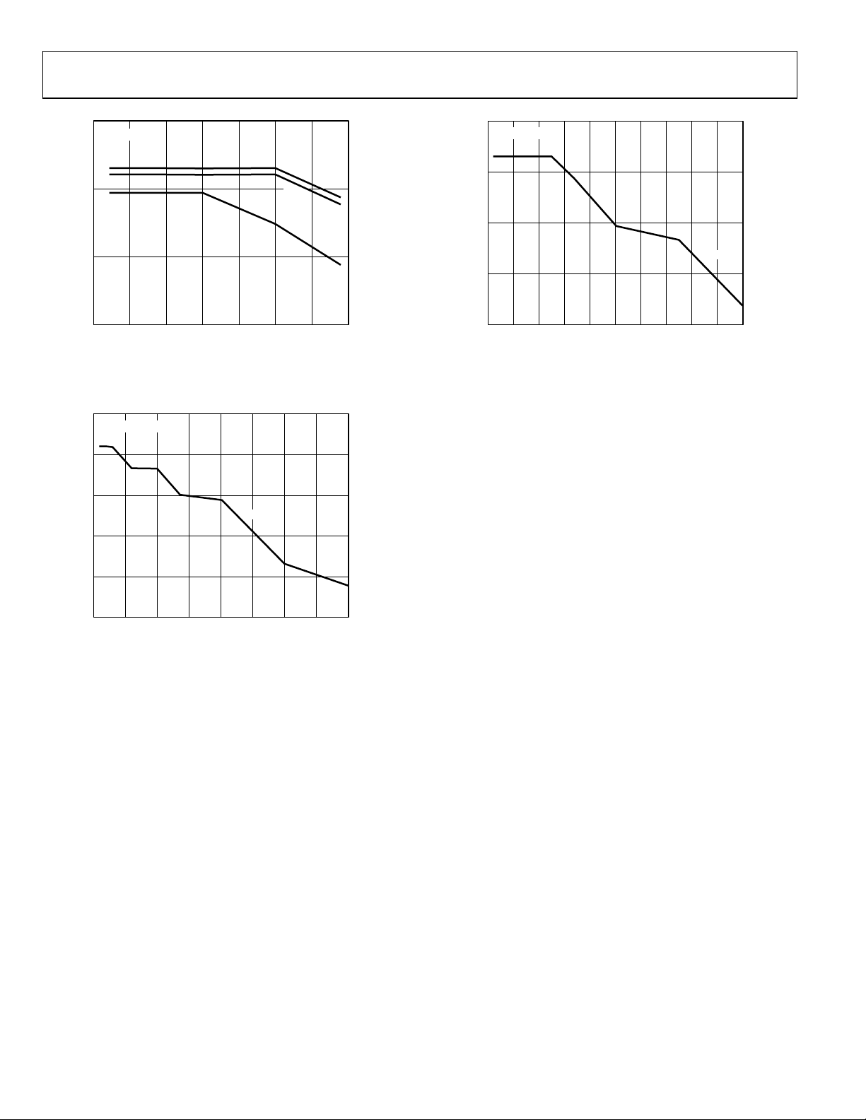
Figure 14. Noise vs. Analog Frequency
90
AIN = –1dBFS
85
80
25°C
75
03198-0-068
90
88
SNR (dB) [BW = 150kHz]
86
84
0 20 40 60 80 100 120 140 160 180 200
ANALOG INPUT FREQUENCY (MHz)
Figure 16. Noise vs. Analog Frequency (IF)
25°C
03198-0-067
70
WORST-CASE HARMONIC (dBc)
65
75 100 125 150 175 20025 500
ANALOG FREQUENCY (MHz)
03198-0-069
Figure 15. Harmonics vs. Analog Frequency
Rev. 0 | Page 16 of 76
AD6652
K
K
DDC TIMING DIAGRAMS
t
CLK
t
CLKL
CL
t
CLKH
t
DLI
LIA, LIB
LIA, LIB
03198-0-065
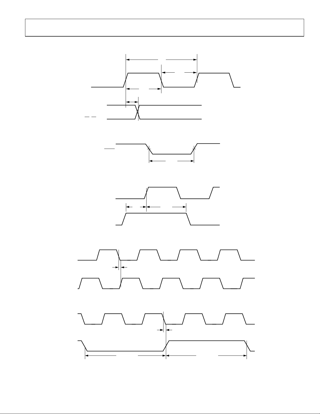
Figure 17. Level Indicator Output Switching Characteristics
RESET
t
RESL
03198-0-003
Figure 18. Reset Timing Requirements
CLK
t
HS
03198-0-006
SYNCA
SYNCB
SYNCC
SYNCD
t
SS
Figure 19. SYNC Timing Inputs
CLK
t
DPOCLKL
PCL
03198-0-007
Figure 20. PCLK to CLK Switching Characteristics Divide-by-1
CLK
t
DPOCLKLL
PCLK
t
POCLKH
t
POCLKL
03198-0-008
Figure 21. PCLK to CLK Switching Characteristics Divide-by-2, -4, or -8
Rev. 0 | Page 17 of 76
AD6652
K
PCLK
PxREQ
PxACK
PCLK
PxACK
t
HPA
t
SPA
03198-0-009
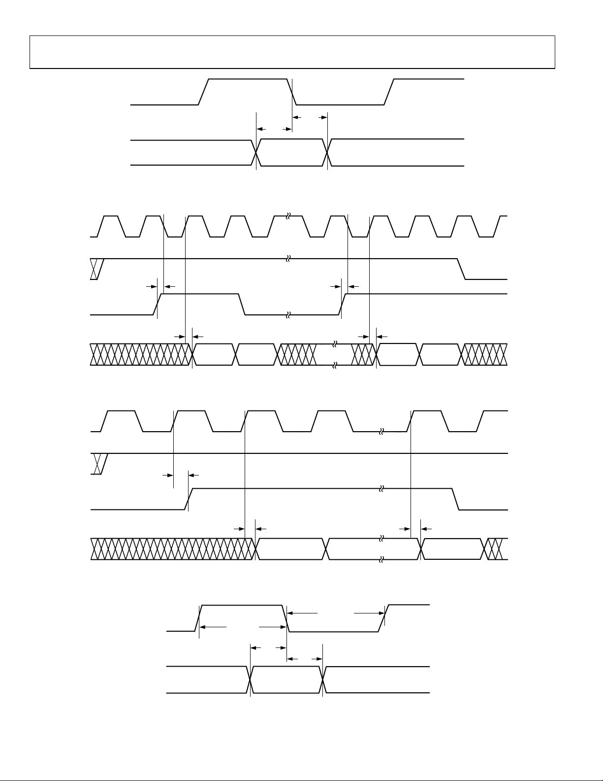
Figure 22. Master Mode PxACK to PCLK Setup and Hold Characteristics
t
SPA
t
SPA
Px[15:0]
t
DPP
DATA 1 DATA 2 DATA N – 1 DATA N
t
DPP
03198-0-010
Figure 23. Master Mode PxACK to PCLK Switching Characteristics
PCLK
PxACK
t
DPREQ
PxREQ
Px[15:0]
t
DPP
DATA 1 DATA N
t
DPP
03198-0-011
Figure 24. Master Mode PxREQ to PCLK Switching Characteristics
t
PCLK
t
POCLKH
POCLKL
t
SPA
PxAC
t
HPA
03198-0-012
Figure 25. Slave Mode PxACK to PCLK Setup and Hold Characteristics
Rev. 0 | Page 18 of 76
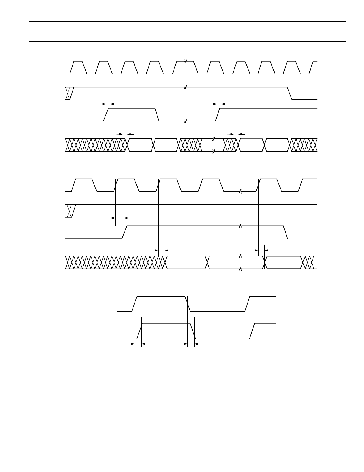
AD6652
PCLK
PxREQ
PxACK
t
SPA
t
SPA
Px[15:0]
t
DPP
DATA 1 DATA 2 DATA N – 1 DATA N
t
DPP
03198-0-013
Figure 26. Slave Mode PxACK to PCLK Switching Characteristics
PCLK
PxACK
t
DPREQ
PxREQ
Px[15:0]
t
DPP
DATA 1 DATA N
t
DPP
03198-0-014
Figure 27. Slave Mode PxREQ to PCLK Switching Characteristics
PCLK
LxCLKOUT
t
RDLCLK
t
FDLCL
03198-0-015
Figure 28. LxCLKOUT to PCLK Switching Characteristics
Rev. 0 | Page 19 of 76
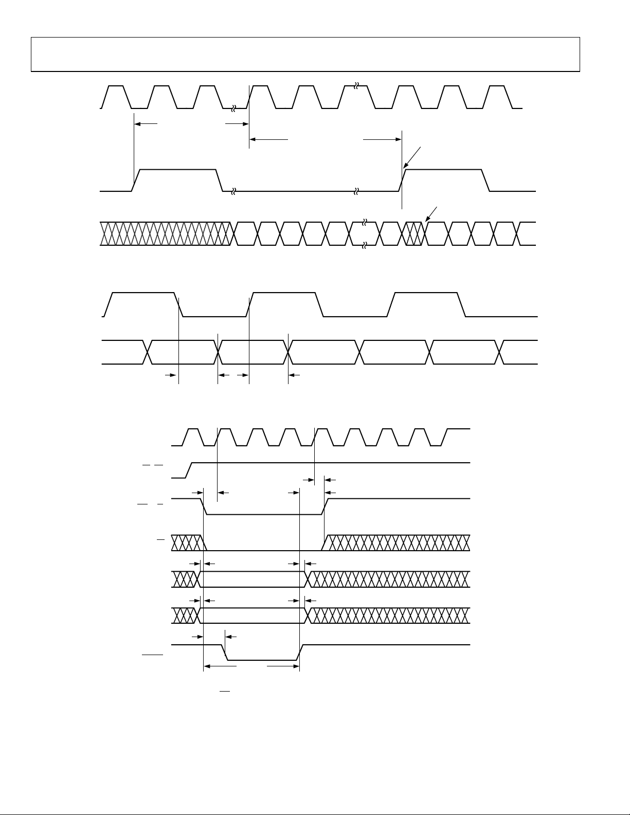
AD6652
LxCLKOUT
LxCLKIN
WAIT ≥ 6 CYCLES
ONE TIME CONNECTIVITY CHECK
8 LxCLKOUT CYCLES
NEXT TRANSFER
ACKNOWLEDGE
NEXT TRANSFER
BEGINS
Lx[7:0]
LxCLKOUT
Lx[7:0]
CLK
RD (DS)
WR (R/W)
Figure 29. LxCLKIN to LxCL
t
FDLCLKDAT
Figure 30. LxCLKOUT to Lx
t
SC
D0
D1
t
RDLCLKDAT
D2 D3 D4 D15 D3
KOUT Data witching Characteristics
S
D0 D1 D2
[7:0] Data Switching Characteristics
t
HC
t
HWR
03198-0-016
03198-0-017
CS
t
t
HAM
HAM
03198-0-018
A[2:0]
D[7:0]
RDY
(DTACK)
t
SAM
VALID ADDRESS
t
SAM
LID DATA
VA
t
DRDY
t
ACC
NOTES
1.
t
ACCESS TIME DEPENDS ON THE ADDRESS ACCESSED. ACCESS TIME IS MEASURED
ACC
FROM FE OF WR TO RE OF RDY.
t
REQUIRES A MAXIMUM OF 9 CLK PERIODS.
2.
ACC
Figure 31. INM Microport Write Timing Requirements
Rev. 0 | Page 20 of 76
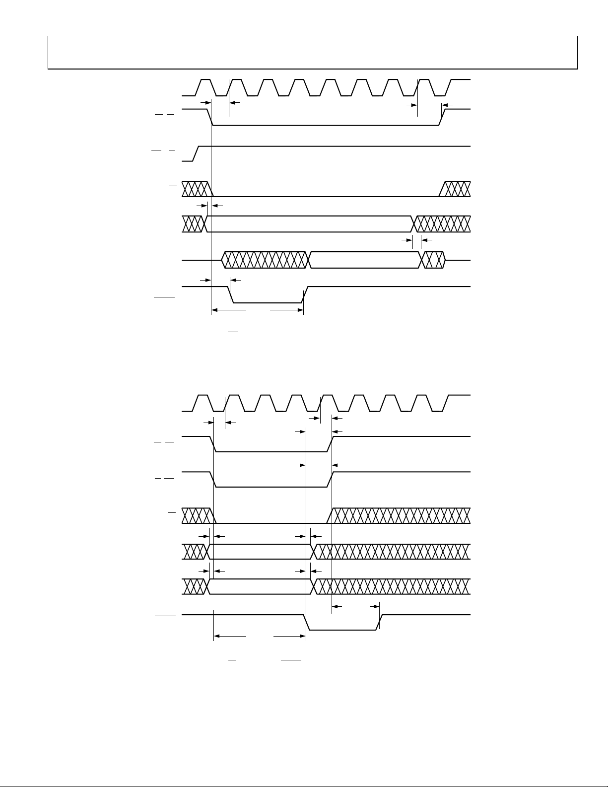
AD6652
CLK
t
RD (DS)
WR (RW)
CS
SC
t
SAM
t
HC
A[2:0]
D[7:0]
RDY
(DTACK)
t
DRDY
NOTES
1.
t
ACCESS TIME DEPEND
ACC
FROM FE OF WR TO RE OF RDY.
t
REQUIRES A MAXIMUM OF 13
2.
ACC
VALID ADDRESS
t
ACC
S ON THE ADDRESS
CLK PERIOD
t
HA
VALID DATA
ACCESSED. ACCESS TIME IS MEASURED
S.
03198-0-019
iming Requirements Figure 32. INM Micropor t Read T
CLK
t
HC
DS (RD)
RW (WR)
t
SC
t
HDS
t
HRW
CS
t
HAM
t
HAM
t
ACC
HE FE OF DTACK.
XIMUM OF 9 CLK PERIODS.
THE ADDRESS ESS TIME IS MEASURED
ort Write Timing Requirements
t
DDTACK
ACCESSED. ACC
03198-0-020
A[2:0]
D[7:0]
DTACK
(RDY)
t
SAM
VALID ADDRESS
t
SAM
NOTES
t
ACCESS TIME DEPENDS ON
1.
ACC
FROM FE OF DS TO T
2.
t
REQUIRES A MA
ACC
Figure 33. MNM Microp
VALID DATA
Rev. 0 | Page 21 of 76
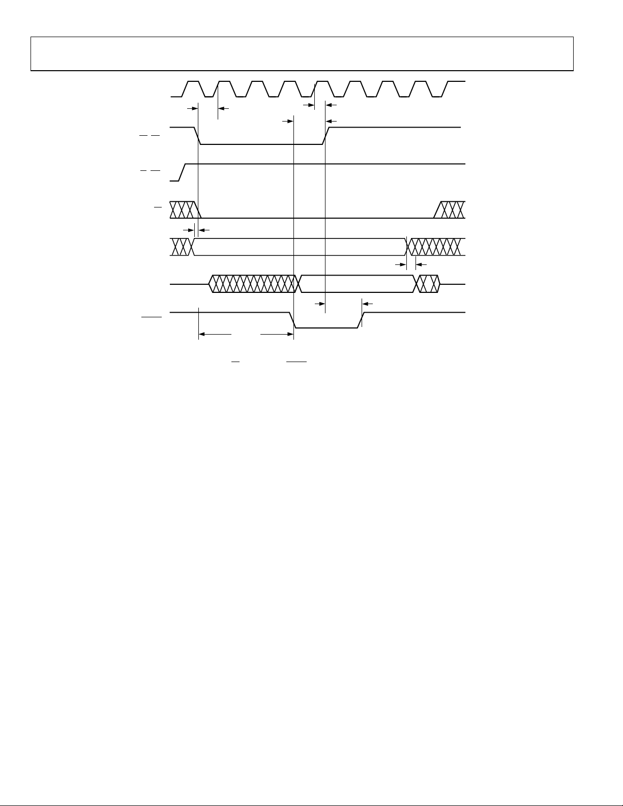
AD6652
CLK
DS (RD)
R/W (WR)
CS
A[2:0]
t
t
SC
t
HDS
t
SAM
HC
VALID ADDRESS
t
HA
D[7:0]
DTACK
(RDY)
t
ACC
NOTES
1.
t
ACCESS TIME DEPENDS ON T
ACC
FROM THE FE OF DS TO THE FE O
t
REQUIRES A MAXIMUM OF 13
2.
ACC
HE ADDRESS ACC
F DTACK.
CLK PERIOD
S.
Timing Requirements Figure 34. MNM Microport Read
VALID DATA
t
DDTACK
ESSED. ACCESS TIME IS MEASURED
03198-0-021
Rev. 0 | Page 22 of 76
AD6652
TERMINOLOGY
Crosstalk
Coupling onto one channel being driven by a (−0.5 dBFS) signal
when the adjacent interfering channel is driven by a full-sc
ale
signal. Measurement includes all spurs resulting from both
direct coupling and mixing components.
IF Sampling (Undersampling)
Due to the effects of aliasing, an ADC is not necessarily limited
to Nyquist sampling. Frequencies above Nyquist are aliased and
appear in the first Nyquist zone (dc to Sample Rate/2). Care
must be taken to limit the bandwidth of the sampled signal so
that it does not overlap Nyq
sam y the bandwidth of the input
pling performance is limited b
HA (sample-and-hold amplifier) and clock jitter. (Jitter adds
S
uist zones and alias onto itself. IF
more noise at higher input frequencies.)
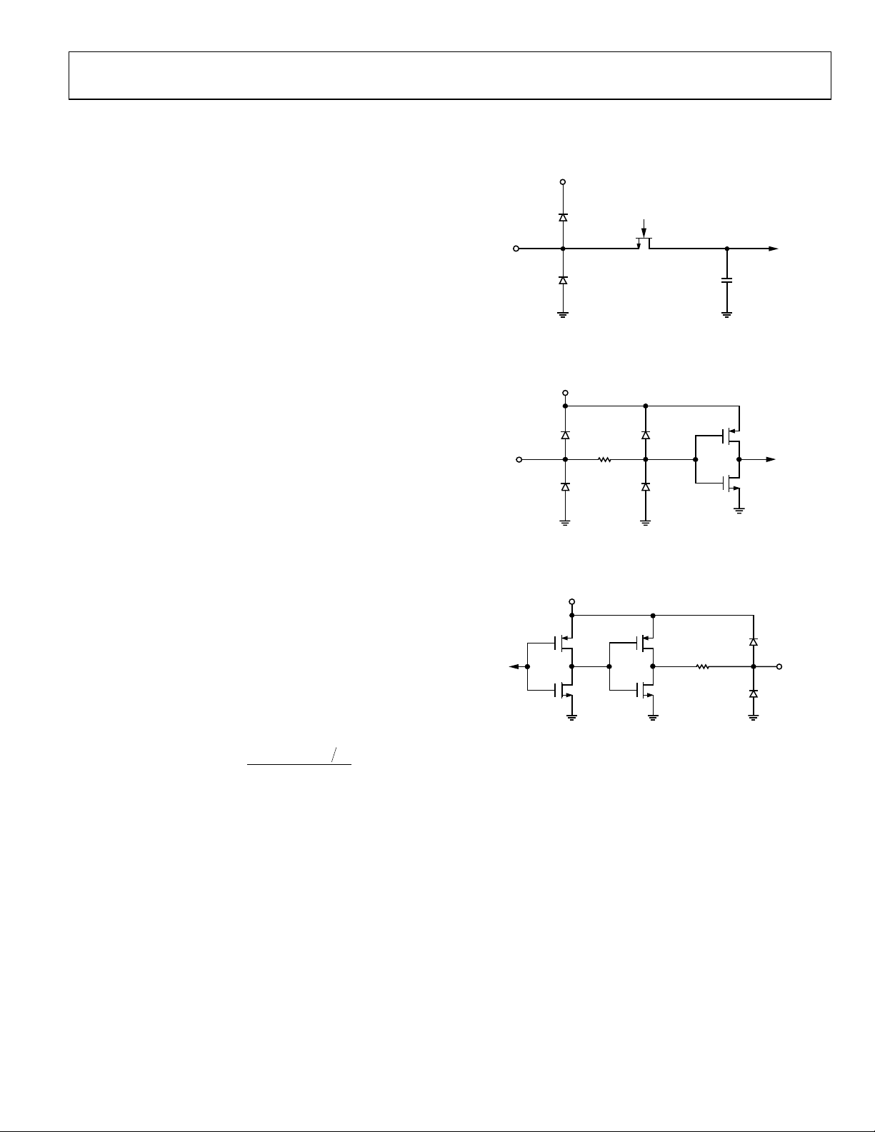
ADC EQUIVALENT CIRCUITS
AVDD
Figure 35. Analog Input Circuit
AVDD
03198-0-022
Nyquist Samplin ling)
Oversampling occu frequen f the
analog input signal are be e Nyqu
and requires that the analo ut frequency b at least
g (Oversamp
rs when the cy components o
low th ist frequency (F
g inp e sampled
/2),
clo
ck
two samples per cycle.
ut-of-Range Recovery Time
O
Out-of-range recovery time is th time it takes for the analogto-digital co after a
transient fro ove
nverter (ADC) to reacquire the analog input
m 10% above positive full scale to 10% ab
e
negative full scale, or from 10% below negative full scale to 10%
below positive full scale.
Processing Gain
When the tuned channel occupies less bandwidth than the
input signal, this rejection of out-of-band noise is referred to as
processing gain. By using large decimation factors, this processing gain can improve the SNR of the ADC by 20 dB or more.
The following equation can be used to estimate processing gain:
RateSample
2_
=
_GainProcessing
⎡
log10
⎢
⎣
BandwidthFilter
_
⎤
⎥
⎦
Signal-to-Noise Ratio (SNR)
The ratio of the rms value of the measured input signal to the
rms sum of all other spectral components within the programmed DDC filter bandwidth, excluding the first six
harmonics
cibels (dB).
de
and dc. The value for SNR is expressed in
03198-0-023
Figure 36. Digital Input
VDD
03198-0-024
Figure 37. Digital Output
Two -Ton e I MD Rejection
The ratio of the rms value of either input tone to the rms value
of the worst third-order intermodulation product; reported
in dBc.
Rev. 0 | Page 23 of 76
 Loading...