


OUTPUT
NONINVERTING
INPUT
OUTPUT
INVERTING
INPUT
INVERTING
INPUT
NONINVERTING
INPUT
–V
3
4
5
6
7
8
1
2
+V
TOP
VIEW
NOTE:
PIN 4 CONNECTED TO CASE
AMPLIFIER NO. 1 AMPLIFIER NO. 2
Dual High Speed,
a
FEATURES
Matched Offset Voltage
Matched Offset Voltage Over Temperature
Matched Bias Currents
Crosstalk –124 dB at 1 kHz
Low Bias Current: 35 pA max Warmed Up
Low Offset Voltage: 500 mV max
Low Input Voltage Noise: 2 mV p-p
High Slew Rate: 13 V/ms
Low Quiescent Current: 4.5 mA max
Fast Settling to 60.01%: 3 ms
Low Total Harmonic Distortion: 0.0015% at 1 kHz
Standard Dual Amplifier Pinout
Available in Hermetic Metal Can Package
and Chip Form
MIL-STD-883B Processing Available
Single Version Available: AD544
PRODUCT DESCRIPTION
The AD644 is a pair of matched high speed monolithic FET input operational amplifiers fabricated with the most advanced bipolar, JFET and laser-trimming technologies. The AD644 offers
matched bias currents that are significantly lower than currently
available monolithic dual BiFET operational amplifiers: 35 pA
max, matched to 25 pA for the AD644K and L, 75 pA max
matched to 35 pA for the AD644J and S. In addition, the offset
voltage is laser trimmed to less than 0.5 mV, and matched to
0.25 mV for the AD644L, 1.0 mV and matched to 0.5 mV for
the AD644K, utilizing Analog Devices’ laser-wafer trimming
(LWT) process.
The tight matching and temperature tracking between the operational amplifiers is achieved by ion-implanted JFETs and
laser-wafer trimming. Ion-implantation permits the fabrication
of precision, matched JFETs on a monolithic bipolar chip. This
process optimizes the ability to produce matched amplifiers
which have lower initial bias currents than other popular BiFET
op amps. Laser-wafer trimming each amplifier’s input offset
voltage assures tight initial match and superior IC processing
guarantees offset voltage tracking over the temperature range.
The AD644 is recommended for applications in which both
excellent ac and dc performance is required. The matched amplifiers provide a low cost solution to true wideband instrumentation amplifiers, low dc drift active filters and output amplifiers
for four quadrant multiplying D/A converters such as the
AD7541, 12-bit CMOS DAC.
The AD644 is available in four versions: the “J”, “K” and “L”
are specified over the 0°C to +70°C temperature range and the
“S” over the –55°C to +125°C operating temperature range.
REV. A
Information furnished by Analog Devices is believed to be accurate and
reliable. However, no responsibility is assumed by Analog Devices for its
use, nor for any infringements of patents or other rights of third parties
which may result from its use. No license is granted by implication or
otherwise under any patent or patent rights of Analog Devices.
Implanted BiFET Op Amp
AD644
PIN CONFIGURATION
All devices are packaged in the hermetically sealed, TO-99
metal can or available in chip form.
PRODUCT HIGHLIGHTS
1. The AD644 has tight side to side matching specifications to
ensure high performance without matching individual devices.
2. Analog Devices, unlike some manufacturers, specifies each
device for the maximum bias current at either input in the
warmed-up condition, thus assuring the user that the AD644
will meet its published specifications in actual use.
3. Laser-wafer-trimming reduces offset voltage to as low as
0.5 mV max matched side to side to 0.25 mV (AD644L),
thus eliminating the need for external nulling.
4. Improved bipolar and JFET processing on the AD644 result
in the lowest matched bias current available in a high speed
monolithic FET op amp.
5. Low voltage noise (2 µV p-p) and high open loop gain
enhance the AD644’s performance as a precision op amp.
6. The high slew rate (13.0 V/µs) and fast settling time to
0.01% (3.0 µs) make the AD644 ideal for D/A, A/D, sample-
hold circuits and dual high speed integrators.
7. Low harmonic distortion (0.0015%) and low crosstalk
(–124 dB) make the AD644 an ideal choice for stereo audio
applications.
8. The standard dual amplifier pin out allows the AD644 to
replace lower performance duals without redesign.
9. The AD644 is available in chip form.
One Technology Way, P.O. Box 9106, Norwood, MA 02062-9106, U.S.A.
Tel: 617/329-4700 Fax: 617/326-8703
AD644–SPECIFICA TIONS
(@ +258C and VS = 615 V dc)
Model AD644J AD644K AD644L AD644S
Min Typ Max Min Typ Max Min Typ Max Min Typ Max Units
OPEN LOOP GAIN
VO = ± 10 V, RL ≥ 2 kΩ 30,000 50,000 50,000 50,000 V/V
T
to T
MIN
, RL = 2 kΩ 20,000 40,000 40,000 20,000 V/V
MAX
OUTPUT CHARACTERISTICS
Voltage @ R
Voltage @ R
Short Circuit Current 25 25 25 25 mA
= 2 kΩ, T
L
= 10 kΩ, T
L
MIN
MIN
to T
to T
610 ±12 610 ±12 610 ±12 610 ±12 V
MAX
612 ±13 612 ±13 612 ±13 612 ±13 V
MAX
FREQUENCY RESPONSE
Unity Gain Small Signal 2.0 2.0 2.0 2.0 MHz
Full Power Response 200 200 200 200 kHz
Slew Rate, Unity Gain 8.0 13.0 8.0 13.0 8.0 13.0 8.0 13.0 V/µs
Total Harmonic Distortion 0.0015 0.0015 0.0015 0.0015 %
INPUT OFFSET VOLTAGE
1
Initial Offset 2.0 1.0 0.5 1.0 mV
Input Offset Voltage T
Input Offset Voltage vs. Supply,
T
to T
MIN
MAX
INPUT BIAS CURRENT
MIN
2
to T
MAX
3.5 2.0 1.0 3.5 mV
200 100 100 100 µV/V
Either Input 10 75 10 35 10 35 10 35 pA
Offset Current 10 5 5 5 pA
MATCHING CHARACTERISTICS
3
Input Offset Voltage 1.0 0.5 0.25 0.5 mV
Input Offset Voltage T
Input Bias Current 35 25 25 35 pA
MIN
to T
MAX
3.5 2.0 1.0 3.5 mV
Crosstalk –124 –124 –124 –124 dB
INPUT IMPEDANCE
Differential 10
Common Mode 1012i310
INPUT VOLTAGE RANGE
Differential
4
12
i610
12
i610
12
i310
12
i610
12
i310
12
i6MΩipF
12
i3MΩipF
±20 ±20 ±20 ±20 V
Common Mode ± 10 ±12 ± 10 ±12 ±10 ±12 ± 10 ± 12 V
Common-Mode Rejection 76 80 80 80 dB
INPUT NOISE
Voltage 0.1 Hz to 10 Hz 2222µV p-p
f = 10 Hz 35 35 35 35 nV/√
f = 100 Hz 22 22 22 22 nV/√
f = 1 kHz 18 18 18 18 nV/√
Hz
Hz
Hz
f = 10 kHz 16 16 16 16 nV/√Hz
POWER SUPPLY
Rated Performance ± 15 ±15 ± 15 ±15 V
Operating ± 5 ±18 ±5 ±18 ±5 ± 18 ± 5 ±18 V
Quiescent Current 3.5 4.5 3.5 4.5 3.5 4.5 3.5 4.5 mA
TEMPERATURE RANGE
Operating, Rated Performance 0 +70 0 +70 0 +70 –55 +125 °C
Storage –65 +150 –65 +150 –65 +150 –65 +150 °C
PACKAGE OPTION
TO-99 Style (H-08B) AD644JH AD644KH AD644LH AD644SH
Chips AD644JChips AD644KChips AD644SChips
NOTES
1
Input Offset Voltage specifications are guaranteed after 5 minutes of operation at TA = +25°C.
2
Bias Current specifications are guaranteed at maximum at either input after 5 minutes of operation at TA = +25°C. For higher temperatures, the current doubles every 10°C.
3
Matching is defined as the difference between parameters of the two amplifiers.
4
Defined as voltage between inputs, such that neither exceeds ±10 V from ground.
Specifications shown in boldface are tested on all production units at final electrical test. Results from those tests are used to calculate outgoing quality levels. All min and max specifications
are guaranteed, although only those shown in boldface are tested on all production units.
Specifications subject to change without notice.
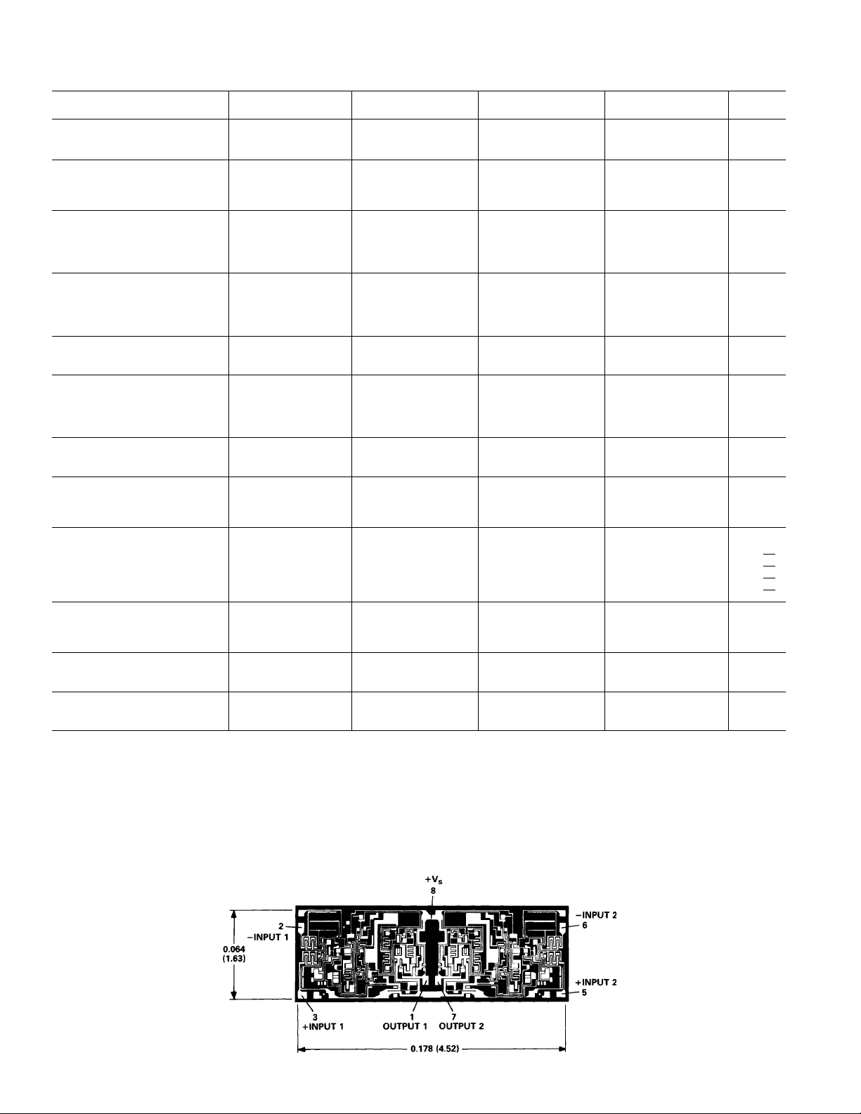
METALIZATION PHOTOGRAPH
Dimensions shown in inches and (mm).
Contact factory for latest dimensions.
–2–
REV. A
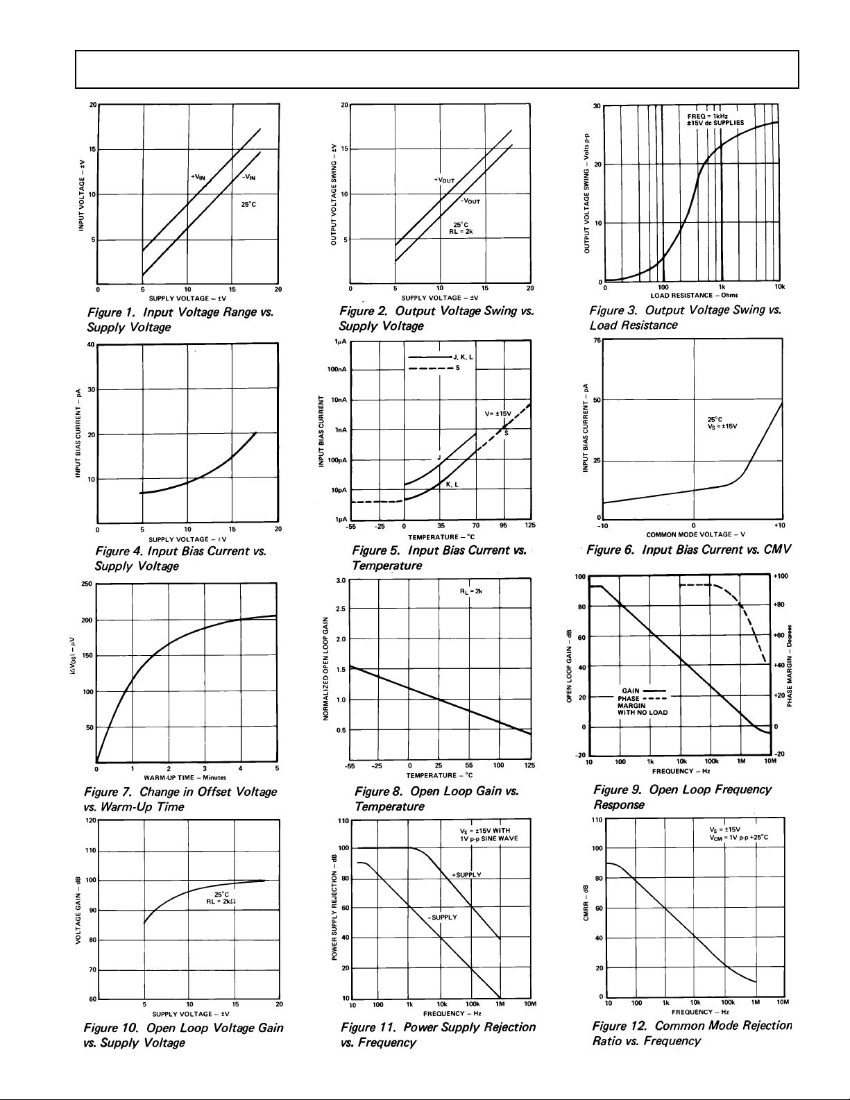
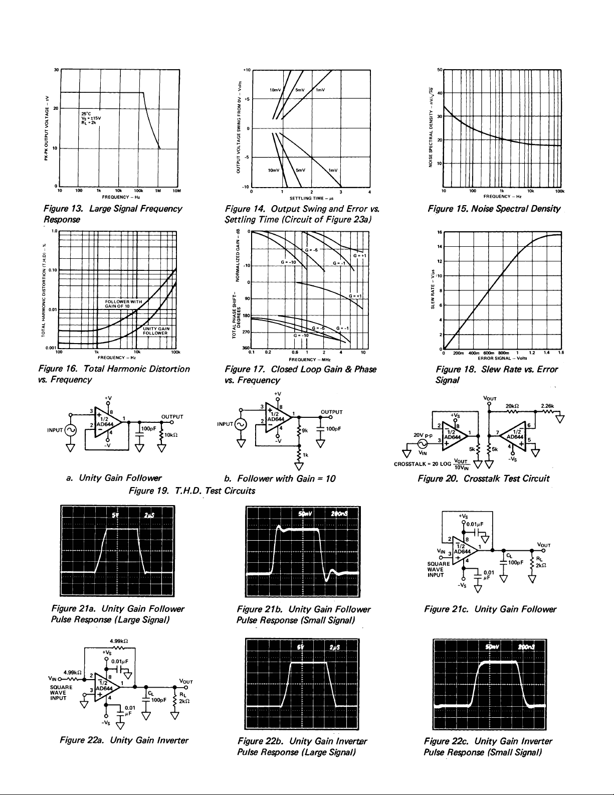
T ypical Characteristics–AD644
REV. A
–3–
AD644
–4–
REV. A

AD644
low pass filter formed by the 100 Ω series resistor and the load
capacitance, C
The low input bias current (35 pA), low noise, high slew rate
and high bandwidth characteristics of the AD644 make it suitable for electrometer applications such as photodiode preamplifiers and picoampere current-to-voltage converters. The use of
guarding techniques in printed circuit board layout and construction is critical for achieving the ultimate in low leakage performance that the AD644 can deliver. The input guarding
scheme shown in Figure 25 will minimize leakage as much as
possible. The same layout should be used on both sides of a
double side board. The guard ring is connected to a low impedance potential at the same level as the inputs. High impedance
signal lines should not be extended for any unnecessary length
on a printed circuit; to minimize noise and leakage, such conductors should be replaced by rigid shielded cables.
.
L
The fast settling time (3.0 µs to 0.01% for 20 V p-p step) and
low offset voltage make the AD644 an excellent choice as an
output amplifier for current output D/A converters such as the
AD7541. The upper trace of the oscilloscope photograph of Figure 23b shows the settling characteristics of the AD644. The
lower trace represents the input to Figure 23a. The AD644 has
been designed for fast settling to 0.01%, however, feedback
components, circuit layout and circuit design must be carefully
considered to obtain the optimum settling time.
Figure 25. Board Layout for Guarding Inputs
INPUT PROTECTION
The AD644 is guaranteed for a maximum safe input potential
equal to the power supply potential. The input stage design also
allows differential input voltages of up to ± 1 volt while maintaining the full differential input resistance of 10
makes the AD644 suitable for comparator situations employing
a direct connection to high impedance source.
Many instrumentation situations, such as flame detectors in gas
chromatographs, involve measurement of low level currents
from high voltage sources. In such applications, a sensor fault
condition may apply a very high potential to the input of the
current-to-voltage converting amplifier. This possibility necessitates some form of input protection. Many electrometer type
devices, especially CMOS designs, can require elaborate Zener
protection schemes which often compromise overall performance.
The AD644 requires input protection only if the source is not
current-limited, and as such is similar to many JFET-input
designs. The failure mode would be overheating from excess
current rather than voltage breakdown. If the source is not
current-limited, all that is required is a resistor in series with the
affected input terminal so that the maximum overload current is
1.0 mA (for example, 100 kΩ for a 100 volt overload). This
simple scheme will cause no significant reduction in performance and give complete overload protection. Figure 26 shows
proper connections.
12
Ω. This
The circuit in Figure 24 employs a 100 Ω isolation resistor
which enables the amplifier to drive capacitive loads exceeding
500 pF; the resistor effectively isolates the high frequency feedback from the load and stabilizes the circuit. Low frequency
feedback is returned to the amplifier summing junction via the
REV. A
–5–
Figure 26. AD644 Input Protection
AD644
its low input bias current simplifies the resistor (R3, R4) selection for the passband center frequency, circuit Q and voltage
gain.
Figure 28. Band Pass State Variable Filter
The sample and hold circuit, shown in Figure 29 is suitable for
use with 8-bit A/D converters. The acquisition time using a
3900 pF capacitor and fast CMOS SPST (ADG200) switch is
15 µs.
The droop rate is very low 25 × 10
–9
V/µs due to the low input
bias currents of the AD644. Care should be taken to minimize
leakage paths. Leakages around the hold capacitor will increase
the droop rate and degrade performance.
C633b–5–1/85
Figure 27a illustrates the 10-bit digital-to-analog converter,
AD7533, connected for bipolar operation. Since the digital input can accept bipolar numbers and V
can accept a bipolar
REF
analog input, the circuit can perform a 4-quadrant multiplying
function. The photos exhibit the response to a step input at
V
. Figure 27b is the large signal response and Figure 27c is
REF
the small signal response.
The output impedance of a CMOS DAC varies with the digital
word thus changing the noise gain of the amplifier circuit. The
effect will cause a nonlinearity the magnitude of which is dependent on the offset voltage of the amplifier. The AD644K with
trimmed offset will minimize the effect. The Schottky protection
diodes recommended for use with many older CMOS DACs are
not required when using the AD644.
ACTIVE FILTERS
Literature on active filter techniques and characteristics based
on operational amplifiers is readily available. The successful application of an active filter however, depends on the component
selection to achieve the desired performance. The AD644 is recommended for filters in medical, instrumentation, data acquisition and audio applications, because of its high gain bandwidth
figure, symmetrical slewing, low noise, and low 1 offset voltage.
The state variable filter (Figure 28) is stable, easily tuned and is
independent of circuit Q and gain. The use of the AD644 with
Figure 29. Sample and Hold Circuit
The AD644 in the circuit of Figure 30 provides highly accurate
signal conditioning with high frequency input signals. It provides an offset voltage drift of 10 µV/°C, CMRR of 80 dB over
the range of dc to 10 kHz and a bandwidth of 200 kHz (–3 dB)
at 1 V p-p output. The circuit of Figure 30 can be configured
for a gain range of 2 to 1000 with a typical nonlinearity of
0.01% at a gain of 10.
Figure 30. Wide Bandwidth Instrumentation Amplifier
PRINTED IN U.S.A.
OUTLINE DIMENSIONS
Dimensions shown in inches and (mm).
–6–
REV. A
 Loading...