a
GSM 3 V Transceiver IF Subsystem
AD6432
FEATURES
Fully Compliant with Standard and Enhanced GSM
Specification
DC-350 MHz RF Bandwidths
80 dB Gain Control Range
I/Q Modulation and Demodulation
Onboard Phase Locked Tunable Oscillator
On-Chip Noise Roofing IF Filters
Ultralow Power Design
2.7 V–3.6 V Operating Voltage
User-Selectable Power-Down Modes
Small 44-Lead TQFP Package
Interfaces Directly with AD20msp410 and AD20msp415
GSM Baseband Chipsets
APPLICATIONS
I/Q Modulated Digital Wireless Systems
GSM Mobile Radios
GSM PCMCIA Cards
GENERAL DESCRIPTION
The AD6432 IF IC provides the complete transmit and receive
IF signal processing, including I/Q modulation and demodulation, necessary to implement a digital wireless transceiver such
as a GSM handset. The AD6432 may also be used for other
wireless TDMA standards using I/Q modulation.
The AD6432’s receive signal path is based on the proven architecture of the AD607 and the AD6459. It consists of a mixer,
gain-controlled amplifiers, integrated roofing filter and I/Q
demodulators based on a PLL. The low noise, high-intercept
variable-gain mixer is a doubly-balanced Gilbert-cell type. It has
a nominal –13 dBm input-referred 1 dB compression point and
a 0 dBm input-referred third-order intercept.
The gain-control input accepts an external control voltage input
from an external AGC detector or a DAC. It provides an 80 dB
gain range with 27.5 mV/dB gain scaling, where the mixer and
the IF gains vary together.
The I and Q demodulators provide inphase and quadrature
baseband outputs to interface with Analog Devices’ AD7015
and AD6421 (GSM, DCS1800, PCS1900) baseband converters. An onboard quadrature VCO, externally phase-locked to
the IF signal, drives the I and Q demodulators. The quadrature
phase-locked oscillator (QPLO) requires no external components for frequency control or quadrature generation, and demodulates signals at standard GSM system IFs of 13 MHz, or
26 MHz with a reference input frequency of 13 MHz; or, in
general, 1X or 2X the reference frequency. Maximum reference
frequency is 25 MHz.
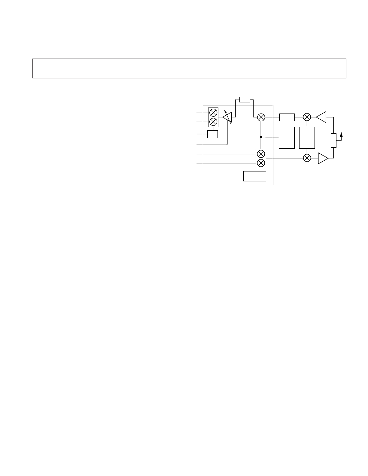
FUNCTIONAL BLOCK DIAGRAM
BP
SAW
PLO
AD6432
This reference signal is normally provided by an external
VCTCXO under the control of the radio’s digital signal
processor. The transmit path consists of an I/Q modulator
and buffer amplifier, suitable for carrier frequencies up to
300 MHz and provides an output power of –17.5 dBm in
a 50 Ω system. The quadrature LO signals driving the
I and Q modulator are generated internally by dividing by
two the frequency of the signal presented at the differential
LO port of the AD6432. In both the transmit and receive
paths, onboard filters provide 30 dB of stopband attenuation.
The AD6432 comes in a 44-lead plastic thin quad flatpack
(TQFP) surface mount package.
OP AMP
IF
SYNTH
RF
SYNTH
PA
REV. 0
Information furnished by Analog Devices is believed to be accurate and
reliable. However, no responsibility is assumed by Analog Devices for its
use, nor for any infringements of patents or other rights of third parties
which may result from its use. No license is granted by implication or
otherwise under any patent or patent rights of Analog Devices.
One Technology Way, P.O. Box 9106, Norwood, MA 02062-9106, U.S.A.
Tel: 617/329-4700 World Wide Web Site: http://www.analog.com
Fax: 617/326-8703 © Analog Devices, Inc., 1997

AD6432–SPECIFICATIONS
(TA = +258C, VP = 3.0 V, GREF = 1.25 V unless otherwise noted)
Parameter Conditions Min Typ Max Units
RX RF MIXER
RF Input Frequency 350 MHz
AGC Conversion Gain Variation Z
Input 1 dB Compression Point At V
Input Third-Order Intercept At V
SSB Noise Figure At Z
= 150 Ω: 0.2 V < V
IN
= 2.4 V, Z
GAIN
= 0.2 V, RFIN = –25 dBm 0 dBm
GAIN
= 150 Ω, F
IN
RF
FLO = 272 MHz, V
< 2.4 V –3 to +15 dB
GAIN
= 150 Ω –13 dBm
IN
= 246 MHz,
= 0.2 V 10 dB
GAIN
RX IF AMPLIFIER
AGC Gain Variation 0.2 V < V
Input Resistance at V
GAIN
< 2.4 V –14 to 48 dB
GAIN
= 0.2 V 5 kΩ
Operating Frequency Range 10 50 MHz
GAIN CONTROL
Total Gain Control Range Mixer+IF+Demod, 0.2 V < V
< 2.4 V 80 dB
GAIN
Control Voltage Range at GAIN 0.2 2.4 V
Gain Scaling 27.5 mV/dB
Gain Law Conformance ±0.1 dB
Bias Current at GREF –0.5 µA
Input Resistance at Gain 20 kΩ
INTEGRATED IF FILTER
BPF Center Frequency f
IFS0 = 1 “0” = Connect to Ground, “1” = Connect to V
IFS0 = 0 “0” = Connect to Ground, “1” = Connect to V
BPF –3 dB BW f
IFS0 = 1 “0” = Connect to Ground, “1” = Connect to V
IFS0 = 0 “0” = Connect to Ground, “1” = Connect to V
= 13 MHz
REF
= 13 MHz
REF
P
P
P
P
13 MHz
26 MHz
5 MHz
10 MHz
I AND Q DEMODULATOR
Demodulation Gain 17 dB
Output Voltage Range Differential 0.3 V
– 0.2 V
POS
Output Voltage Common-Mode Level Not Power Supply Independent 1.5 V
Output Offset Voltage Differential, V
= GREF –150 +150 mV
GAIN
Error in Quadrature Differential from I to Q, IF = 13 MHz 1 3.5 Degrees
Amplitude Match 0.25 dB
I/Q Output BW C
= 10 pF 3 MHz
LOAD
Output Resistance Each Pin 4.7 kΩ
QUADRATURE IF PLL
Operating Frequency Range 10 50 MHz
Reference Frequency Voltage Level 200 mV p-p
Reference Frequency Range 25 MHz
Acquisition Time Using 1 kΩ, 1 nF Loop Filter 80 µs
TRANSMIT MODULATOR
Carrier Output Frequency 300 MHz
Output Power R
Input 1 dB Compression Point R
= 150 Ω, Power at Final 50 Ω,
LOAD
F
= 272 MHz –17.5 dBm
IF
= 150 Ω (Differential) 14 dBm
LOAD
I/Q Input Signal Amplitude Differential 2.056 V p-p
I/Q Input Signal Required DC Bias 1.2 V
I/Q Input BW 1 MHz
I/Q Input Resistance 100 kΩ
I/Q Phase Balance With LOs 2nd Harmonic 30 dBc
Bellow Fundamental ±1.5 Degrees
I/Q Amplitude Balance With LOs 2nd Harmonic 30 dBc
Bellow Fundamental ±0.1 dB
Output Harmonic Content R
= 150 Ω –45 (3rd) dBc
LOAD
–65 (5th) dBc
Carrier Feedthrough F
= 272 MHz –33 dBc
CARRIER
Sideband Suppression I and Q Inputs Driven In Quadrature –37 dBc
–2–
REV. 0

AD6432
WARNING!
ESD SENSITIVE DEVICE
Parameter Conditions Min Typ Max Units
LO PORT (LOLO and LOHI)
Input Frequency 200 600 MHz
Input Signal Voltage Range Differential 200 mV p-p
Input Resistance Input Pull-Up Resistors to V
AUXILIARY OP AMPLIFIER
Small Signal –3 dB Bandwidth 50 MHz
Input Signal Voltage Range 0.1 V
Input Offset Voltage ±4mV
Input Bias Current –150 nA
Output Signal Voltage Range With R
> 4 kΩ 0.1 V
LOAD
POWER CONSUMPTION
Supply Voltage 2.7 3 3.6 V
Transmit Mode 13 mA
Receive Mode At V
= 1.2 V 13 mA
GAIN
Sleep Mode < 5 µA
OPERATING TEMPERATURE RANGE –25 +85 °C
NOTES
All reference to dBm is relative to 50 Ω.
Specifications subject to change without notice.
ABSOLUTE MAXIMUM RATINGS
1
Supply Voltage VPDV, VPPX, VPDM, VPFL, VPPC, VPRX,
to CMTX, CMRX, CMIF, CMD . . . . . . . . . . . . . . +3.6 V
Internal Power Dissipation
2
. . . . . . . . . . . . . . . . . . . 600 mW
Operating Temperature Range . . . . . . . . . . . –25°C to +85°C
Storage Temperature Range . . . . . . . . . . . . –65°C to +150°C
Lead Temperature, Soldering (60 sec) . . . . . . . . . . . +300°C
NOTES
1
Stresses above those listed under Absolute Maximum Ratings may cause permanent damage to the device. This is a stress rating only; functional operation of the
device at these or any other conditions above those indicated in the operational
section of this specification is not implied. Exposure to absolute maximum rating
conditions for extended periods may affect device reliability.
2
Thermal Characteristics: 44-lead TQFP package: θJA = 126°C.
ORDERING GUIDE
Temperature Package Package
Model Range Description Option*
(Each Pin) 500 Ω
POS
– 2.1 V
POS
– 0.2 V
POS
PIN CONFIGURATION
VPTX
ITXP
ITXN
QTXP
QTXN
TXPU
PCAP
PCAM
GND
VPPC
CMIF
20
RXPU
21 22
GAIN
PCAO
GREF
33
32
31
30
29
28
27
26
25
24
23
GND
GND
MODO
VPDV
CMTX
LOLO
LOHI
CMRX
GND
RFLO
RFHI
GND
1
2
3
4
5
6
7
8
9
10
11
121314 15 16 17 18 19
VPRX
MXHI
MXLO
(Pins Down)
40 39 3841424344 36353437
AD6432
TOP VIEW
IFHI
IFLO
CMIF
FREF
GND
IFS0
CMDM
FLTR
VPFL
VPDM
IRXP
IRXN
QRXP
QRXN
AD6432AST –25°C to +85°C 44-Pin Plastic ST-44
*ST = Thin Quad Flatpack.
CAUTION
ESD (electrostatic discharge) sensitive device. Electrostatic charges as high as 4000 V readily
accumulate on the human body and test equipment and can discharge without detection.
Although the AD6432 features proprietary ESD protection circuitry, permanent damage may
occur on devices subjected to high energy electrostatic discharges. Therefore, proper ESD
precautions are recommended to avoid performance degradation or loss of functionality.
REV. 0
TQFP
–3–

AD6432
PIN FUNCTION DESCRIPTIONS
Pin Label Description Function
1 GND PCB Ground Not Bonded to IC
2 MODO TX Modulator Output AC Coupled, Drives 150 Ω into 50 Ω
3 VPDV LO2 Divided by 2 Supply Voltage V
4 CMTX On-Chip TX Mixer Common Ground
5 LOLO Differential RX Mixer LO2 Input Negative AC Coupled, V
6 LOHI Differential RX Mixer LO2 Input Positive AC Coupled, V
7 CMRX On-Chip RX Mixer Common Ground
8 GND PCB Ground Not Bonded to IC
9 RFLO Differential RX Mixer IF1 Input Negative AC Coupled
10 RFHI Differential RX Mixer IF1 Input Positive AC Coupled
11 GND PCB Ground Not Bonded to IC
12 VPRX RX Section Supply Voltage V
13 MXHI Differential RX IF1/IF2 Mixer Output Positive See Figure 30
14 MXLO Differential RX IF1/IF2 Mixer Output Negative See Figure 30
15 CMIF On-Chip RX IF2 Common Ground
16 IFLO Differential RX IF2 Input Negative AC Coupled
17 IFHI Differential RX IF2 Input Positive AC Coupled
18 CMIF On-Chip RX IF2 Common Ground
19 RXPU RX Enable (Power-Up) Off = Low < 0.6 V, On = High > 2.5 V
20 GAIN RX VGA Gain Control Input 0.2 V–2.4 V Using 3 V Supply. Max Gain at 0.2 V
21 GREF RX VGA Reference Voltage 1.2 V typ
22 GND PCB Ground Not Bonded to IC
23 QRXN Differential Demodulator Q Output Negative Internal 4.7 kΩ Resistor in Series with the Output
24 QRXP Differential Demodulator Q Output Positive Internal 4.7 kΩ Resistor in Series with the Output
25 IRXN Differential Demodulator I Output Negative Internal 4.7 kΩ Resistor in Series with the Output
26 IRXP Differential Demodulator I Output Positive Internal 4.7 kΩ Resistor in Series with the Output
27 VPDM Demodulator Supply Voltage V
28 VPFL I/Q LO PLL Filter Cap. Supply Voltage To V
29 FLTR I/Q LO PLL Filter Referenced to VPFL
30 CMDM On-Chip Demodulator Common Ground
31 IFS0 IF2 Frequency Select Bit “0” = Low < 0.6 V, “1” = High > 2.5 V
32 GND PCB Ground Not Bonded to IC
33 FREF Reference Input (13 MHz for GSM) AC Coupled. Use 200 mV p-p Input Signal
34 VPPC Auxiliary Op Amp Supply Voltage V
35 PCAO Auxiliary Op Amp Output Active when TXPU Is High
36 GND PCB Ground Not Bonded to IC
37 PCAM Differential Auxiliary Op Amp Input Negative 0.1 V to V
38 PCAP Differential Auxiliary Op Amp Input Positive 0.1 V to V
39 TXPU TX Enable (Power-Up) Low < 0.6 V, High > 2.5 V
40 QTXN Differential Modulator Q Input Negative DC Coupled, 1.2 V ± 514 mV
41 QTXP Differential Modulator Q Input Positive DC Coupled, 1.2 V ± 514 mV
42 ITXN Differential Modulator I Input Negative DC Coupled, 1.2 V ± 514 mV
43 ITXP Differential Modulator I Input Positive DC Coupled, 1.2 V ± 514 mV
44 VPTX TX Section Supply Voltage V
POS
POS
POS
POS
POS
with Good Decoupling
POS
POS
– 2.1 V
POS
– 2.1 V
POS
POS
to V
– 100 mV
POS
– 100 mV to V
POS
–4–
REV. 0

PCAP
TXPU
QTXN
QTXP
ITXN
ITXP
MODO
LOLO
RFHI
TXPU
IFS0
RXPU
4.7
DECOUPLING
VS1
C7
F
VS1
J1
J3
J4
J5
VPDV
6
4
AD6432
R30
49.9Ω
C9
F
0.1
R12
100pF
0Ω
C28
0.1
C2
F
R23
123Ω
C15
100pF
GND
MODO
VPDV
CMTX
LOLO
LOHI
CMRX
GND
RFLO
RFHI
GND
C5
0.01
F
VPTX
ITXP
1
2
3
4
5
6
7
8
9
10
11
121314 15 16 17 18 19
MXHI
VPRX
ITXN
QTXP
QTXN
40 39 3841424344 363534
AD6432
TOP VIEW
(Pins Down)
IFLO
CMIF
MXLO
VS1
VPTX
DECOUPLING
R9
84Ω
R2
0Ω
C29
0.1
T1
C18
1
F
0.1
2
3
R3
49.9Ω
C14
F
0.01 F
R14
249Ω
C1
100pF
VS2
C7
4.7 F
GREF
GAIN
GND
VS1
MXHI
MXLO
0.1
C30
R31
C3
0Ω
0.01
C44
F
F
C4
0.047 F
R4
49.9Ω
F
C43
F
0.047
0.047
IFLO
TXPU
IFHI
0.047
PCAP
37
CMIF
C7
R11
1kΩ
R10
500Ω
R25
1kΩ
PCAM
GND
20
GAIN
RXPU
F
R5
49.9Ω
R39
OPEN
PCAO
21 22
GREF
C40
0.01
C39
0.01
VPPC
33
32
31
30
29
28
27
26
25
24
23
GND
F
F
FREF
GND
IFS0
CMDM
FLTR
VPFL
VPDM
IRXP
IRXN
QRXP
QRXN
GREF
GAIN
RXPU
IFHI
VS1
C36
1000pF
C10
1000pF
R34
0Ω
C11
0.01
C8
47pF
R1
1kΩ
PCAM
PCAO
R8
0Ω
F
IFS0
0.01
C41
0.01
C32
0.1
C23
F
F
VPPC
DECOUPLING
R32
49.9Ω
R6
0Ω
F
VS2
R7
0Ω
C17
0.1 F
FREF
VS1
IRXP
C6
47pF
IRXN
QRXP
QXRN
REV. 0
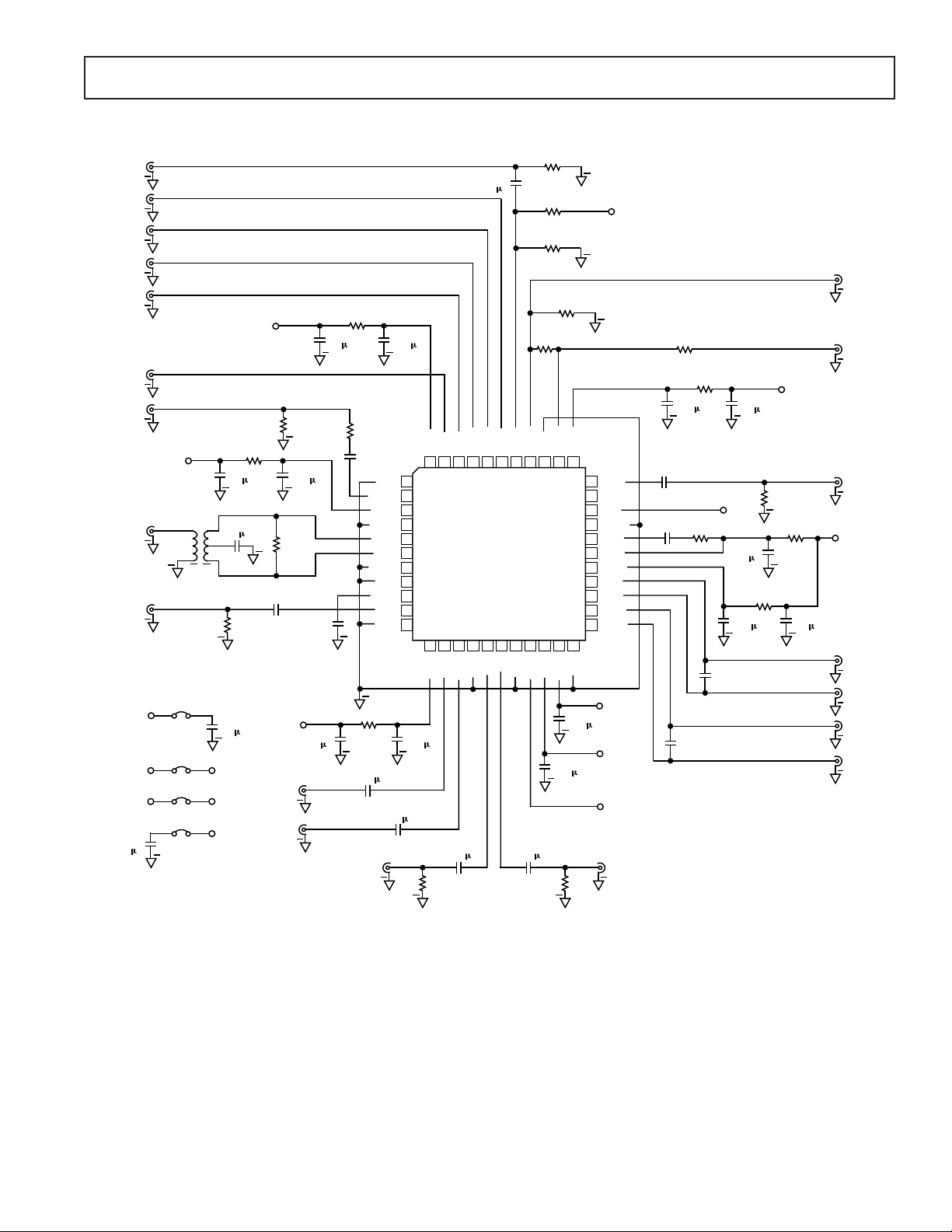
Figure 1. Characterization Board
–5–

AD6432
QTX
VDC
ITX
VDC
VP
10kΩ
0.1µF
INTERFACE BOX TO TEST INSTR
R29
C13
ITX
QTX
MODO
LOIP
RFHI
MXOUT
R22
50Ω
R21
50Ω
1
2
V+
AD1580
V–
R3
20kΩ
R4
20kΩ
NC
VGREF
3
IFIN
FREF
IRX
QRX
PCAP
PCAO
R8
20kΩ
R6
20kΩ
R2
10kΩ
C1 0.1µF
VP
R7
10kΩ
10kΩ
10kΩ
QRX
R1
R5
IRX
QTXN
R9
R10
25Ω
R12
25Ω
C4
0.1µF
C3
0.1µF
C5
0.1µF
C6
0.1µF
10kΩ
C2 1pF
VN
R13
10kΩ
R11
10kΩ
R14
10kΩ
5
V
N
6
A=1
7
8
V
P
5
V
N
6
A=1
7
8
V
P
VN
VN
14
13
12
11
VN
10
9
8
VP
VP
1
2
3
AD824
VP
4
5
6
7
R23
50Ω
R24
50Ω
AD830
AD830
Gm
Gm
Gm
Gm
R17
10kΩ
R15
10kΩ
R16
10kΩ
R18
10kΩ
R20
25Ω
R19
25Ω
4
3
2
1
4
3
2
1
QTXP
VDC
ITXP
ITXN
IRXN
IRXP
QRXN
QRXP
VS1
VS2
GND
VP
VN
GAIN
INTERFACE BOX TO CHAR BOARD
ITXP
ITXN
QTXP
QTXN
MODO
LOIP
VS2
IFS1
IFS0
RXPU
VS1
3
3
J1
2 TXPU
1
2 RXPU
1
RFHI
MXHI
MXLO
IFLO
IFHI
FREF
GND
TXPU
GAIN
GREF
GND
IRXP
IRXN
QRXP
QRXN
PCAP
PCAO
MXOUT
IFIN
NOTES:
VP = +5V
VN = –5V
R25
50Ω
R26
50Ω
VN
AD830
5
V
C8
0.1µF
VP
C7
0.1µF
VP
N
6
A=1
7
8
V
P
1
Gm
2
3
Gm
4
AD830
1
Gm
2
3
Gm
4
AD830
Gm
Gm
A=1
A=1
IFS0
4
3
R30
20kΩ
2
1
R31
20kΩ
V
8
7
6
5
V
8
P
7
6
5
V
N
C9
0.1µF
C11
0.1µF
C10
0.1µF
C12
0.1µF
P
V
N
V
P
V
N
R27
50Ω
R28
50Ω
MXLO
MXHI
IFHI
IFLO
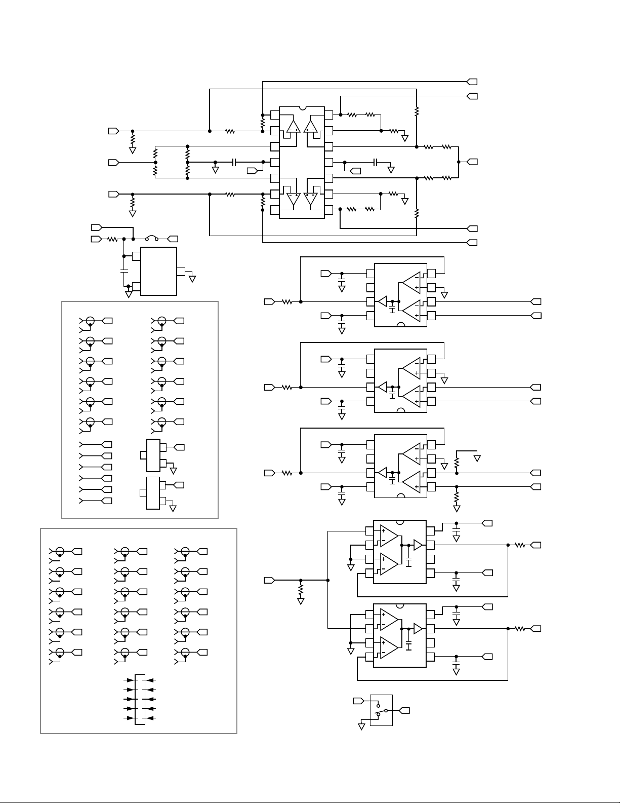
Figure 2. Characterization Test Set
–6–
REV. 0
 Loading...