a
PLL
DEMOD
1
IF
VCO
VOLTAGE
REGULATOR
V
REF
MODE
CONTROL
DC
OFFSET
COMP
LIMITER/FILTER
2
AD6402
RSSI
CFILT
DOUT
DFILP
PLLOUT
FMMOD2
FMMOD1
IFIN
TXOUT
TXOUTB
VCO
VREG VBATT SLREF CTL1...3 MODOUT
REFSEL
COFF
REFIN
IF Transceiver Subsystem
AD6402
FEATURES
On-Chip Regulator
PLL Demodulator
On-Chip VCO
No Trims
Excellent Sensitivity
28-Lead SSOP Package
APPLICATIONS
DECT/PWT/WLAN
TDMA FM/FSK Systems
GENERAL DESCRIPTION
The AD6402 is a complete transceiver subsystem for use in
high bit rate radio systems employing FM or FSK modulation.
It is optimized for use in time domain multiple access (TDMA)
systems with communications rates of approximately 1 MBPS.
The AD6402 integrates key functions, including VCOs and a
low drop-out voltage regulator. The AD6402 operates directly
from an unregulated battery supply of 3.1 V to 4.5 V and provides a regulated voltage output which can be used for VCO
supply regulation on a companion RF chip such as the AD6401.
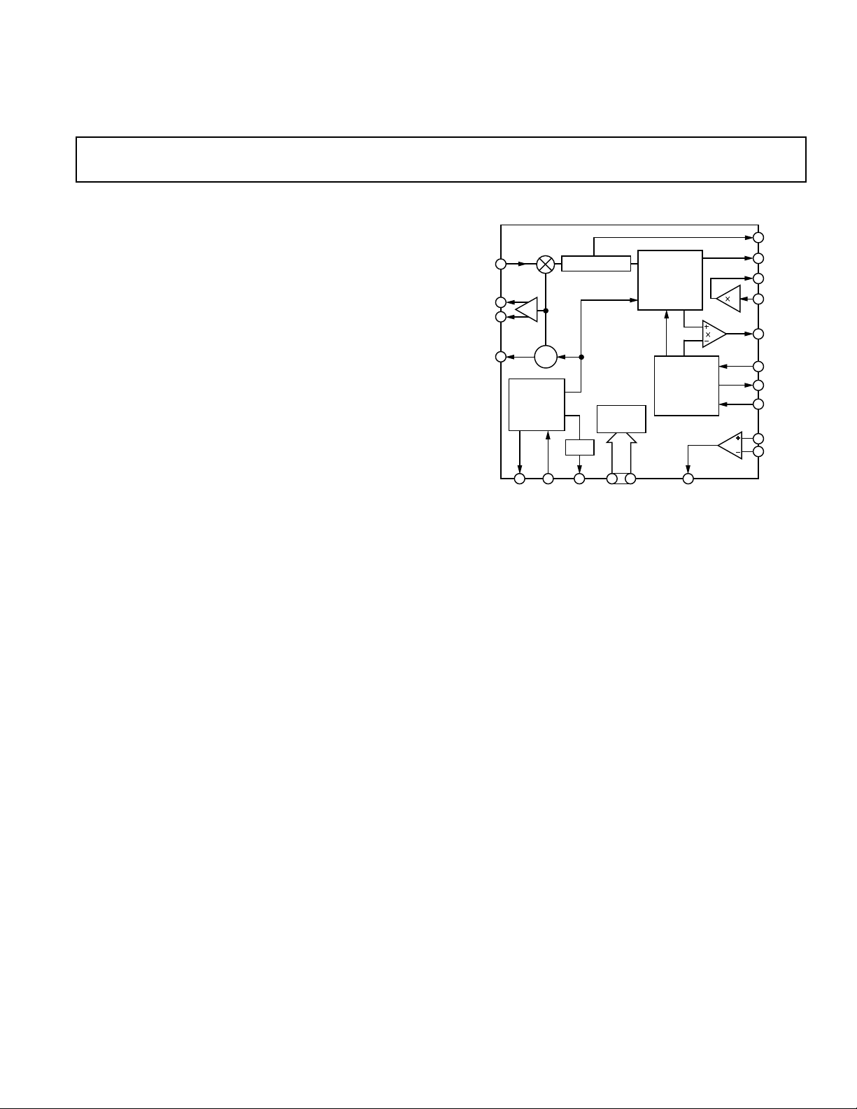
The AD6402 transceiver consists of a mixer, integrated IF
bandpass filter, IF limiter with RSSI detection, VCO, PLL
demodulator and a low dropout voltage regulator. On receive, it
downconverts an IF signal in the 110 MHz range to a second
IF frequency, this frequency being determined by the demodulator reference divide ratios. It then filters, amplifies, and demodulates this signal. The AD6402 provides a filtered baseband
FUNCTIONAL BLOCK DIAGRAM
data output. On transmit, it accepts a Gaussian Frequency Shift
Keying (GFSK) baseband signal, low-pass filters the signal if
required using the on-chip op amp and modulates the IF VCO
by varying the bias voltage on an off-chip varactor diode used in
the tank circuit.
The AD6402 has multiple power-down modes to maximize
battery life. It operates over a temperature range of –25°C to
+85°C and is packaged in a JEDEC standard 28-lead smallshrink outline (SSOP) surface-mount package.
REV. 0
Information furnished by Analog Devices is believed to be accurate and
reliable. However, no responsibility is assumed by Analog Devices for its
use, nor for any infringements of patents or other rights of third parties
which may result from its use. No license is granted by implication or
otherwise under any patent or patent rights of Analog Devices.
One Technology Way, P.O. Box 9106, Norwood, MA 02062-9106, U.S.A.
Tel: 617/329-4700 World Wide Web Site: http://www.analog.com
Fax: 617/326-8703 © Analog Devices, Inc., 1997

AD6402–SPECIFICA TIONS
AD6402ARS
Parameter Conditions Min Typ Max Units
IF BANDPASS FILTER
Center Frequency Rejection REFIN = 13.824 MHz, REFSEL <0.2 V
F
±3.0 MHz 7 dBc
O
F
±4.7 MHz 13 dBc
O
F
±6.0 MHz 16 dBc
O
CC
Stop Band Rejection 30 dBc
RECEIVER
Sensitivity FM Modulated 576 kHz, FM Deviation 288 kHz –80 dBm
BT = 0.5, Demod Output SNR = 10 dB, RS = 150 Ω
RSSI
Low V
High V
Slope See Figure 4 20 mV/dB
= 0.2 V, RS = 150 Ω –85 dBm
OUT
= 1.8 V, RS = 150 Ω –5 dBm
OUT
Output Impedance 4kΩ
DEMODULATOR
Gain At Data Filter Output 1.2 1.55 V/MHz
Offset Referred to SLREF –200 +200 mV
Lock Time From SLEEP Mode 200 µs
From RXLOCK Mode 20 µs
DATA FILTER OP AMP
Gain 2
Slew Rate C
Gain Bandwidth C
Output Swing Low 0.2 V
= 30 pF 8 V/µs
LOAD
= 30 pF 15 MHz
LOAD
Output Swing High V
Output Impedance 50 Ω
IF VCO
Frequency Note 1 131 MHz
SSB Phase Noise @ 5 MHz Offset –139 dBc/Hz
Output Power Differential R
= 300 Ω –12 dBm
LOAD
2nd Harmonic –22 dB
3rd Harmonic –24 dB
TRANSMIT FILTER OP AMP
Open Loop Gain 75 dB
Unity Gain Bandwidth C
Output Slew Rate C
= 30 pF 12 MHz
LOAD
= 30 pF 5 V/µs
LOAD
Minimum Input Voltage 1V
Maximum Input Voltage V
Minimum Output Voltage 0.2 V
Maximum Output Voltage VCC–0.2 V
POWER CONTROL
Logical High Threshold 0.8 × V
Logical Low Threshold 0.2 × V
Turn-On Response Time VCC Steady State 0.5 µs
VOLTAGE REFERENCE
SLREF 1.3 1.5 V
SUPPLY REGULATOR
Output Voltage For Battery Voltages from 3.1 V to 4.5 V 2.75 2.95 V
Turn-On Time 1 mV Settling, C
= 100 nF 200 µs
LOAD
Line Regulation 200 mV Battery Step; 5 mV Settling 1 µs
Load Regulation 10 µA to 30 mA Step; 5 mV Settling 200 µs
POWER SUPPLY All V
at 2.85 V
CC
Supply Current RXLOCKP 30 mA
RXLOCK 17 mA
RXDEMOD 26 mA
TRANSMIT 6 mA
STANDBY
SLEEP 10 µA
NOTES
1
Using test tank circuit as shown.
Specifications subject to change without notice.
20.736 MHz
–0.2 V
CC
–0.2 V
CC
CC
CC
V
V
300 µA
–2– REV. 0

AD6402
WARNING!
ESD SENSITIVE DEVICE
RECOMMENDED OPERATING CONDITIONS
VBAT . . . . . . . . . . . . . . . . . . . . . . . . . . . . . . . . . 3.1 V–4.5 V
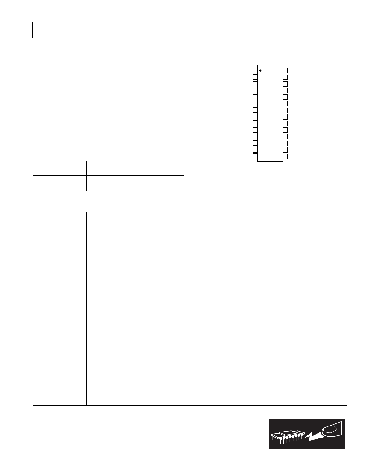
PIN CONFIGURATION
IFVCC1, IFVCC2, PLLVCC . . . . . . . . . . . . . . . . . . . .2.85 V
Operating Temperature Range . . . . . . . . . . . –25°C to +85°C
ABSOLUTE MAXIMUM RATINGS*
Supply Voltage . . . . . . . . . . . . . . . . . . . . . . . . . . . . . . . +5.5 V
Storage Temperature Range . . . . . . . . . . . . –65°C to +150°C
Lead Temperature, Soldering (60 sec) . . . . . . . . . . . .+300°C
*Stresses above those listed under Absolute Maximum Ratings may cause perma-
nent damage to the device. This is a stress rating only; functional operation of the
device at these or any other conditions above those indicated in the operational
section of this specification is not implied. Exposure to absolute maximum rating
conditions for extended rating conditions for extended periods may affect device
reliability.
Thermal Characteristics:
28-lead SSOP package: θJA = 109°C/W.
ORDERING GUIDE
MODOUT
FMMOD2
FMMOD1
VCOGND
TXOUTB
VCO
VREG
VBAT
CTL3
CTL2
CTL1
CFILT
COFF
REXT
1
2
3
4
5
AD6402
6
TOP VIEW
(Not to Scale)
7
8
9
10
11
12
13
14
28
27
26
25
24
23
22
21
20
19
18
17
16
15
TXOUT
REFSEL
IFVCC1
IFIN
IFGND
RSSI
IFVCC2
PLLGND
PLLVCC
SLREF
DOUT
DFILP
PLLOUT
REFIN
Temperature Package
Model Range Description
AD6402ARS –25°C to +85°C 28-Lead SSOP
AD6402ARS-REEL –25°C to +85° C 28-Lead SSOP
PIN FUNCTION DESCRIPTIONS
Pin Mnemonic Function
1 TXOUTB Transmit IF VCO Buffer Inverting Output
2 MODOUT Frequency Modulator Filter Op Amp Output
3 FMMOD2 Frequency Modulator Filter Op Amp Noninverting input
4 FMMOD1 Frequency Modulator Filter Op Amp Inverting input
5 VCOGND IF VCO Ground
6 VCO IF VCO Tank Connection
7 VREG Regulated Supply Output for RF VCO (Supplies Internal IF VCO, Mode Control, Bandgap Reference,
and COFF Buffer)
8 VBAT Battery Supply Voltage Input to Internal Regulator and COFF Charge Pump
9 CTL3 Mode Control Input 3, CMOS Logical Level
10 CTL2 Mode Control Input 2, CMOS Logical Level
11 CTL1 Mode Control Input 1, CMOS Logical Level
12 CFILT PLL Demodulator Loop Filter Capacitor
13 COFF PLL Demodulator Frequency Offset Voltage Track/Hold Capacitor
14 REXT External Current-Setting Resistor
15 REFIN Baseband Reference Frequency Input, 100 mV p-p, AC Coupled
16 PLLOUT PLL Demodulator Output
17 DFILP Data Filter Voltage-Follower Input
18 DOUT Data Filter Voltage-Follower Output
19 SLREF PLL Demodulator Output DC Reference Voltage
20 PLLVCC PLL Demodulator and Data Filter Supply Input
21 PLLGND PLL Demodulator and Data Filter Ground
22 IFVCC2 IF Limiter Supply Input 1
23 RSSI RSSI Output
24 IFGND IF Stage, Mixer, Band Pass Filter, IF VCO Buffer, Tx Op Amp, Mode Control, and Regulator Ground
25 IFIN IF Mixer Input, Z
= 150 Z
O
26 IFVCC1 IF Mixer, Limiter 1, IF Filter, IF VCO Buffer
27 REFSEL Reference Frequency Select; IF = 1.5× or 2.5× Reference Frequency, CMOS Logical Level Input
28 TXOUT Transmit IF VCO Buffer Output
CAUTION
ESD (electrostatic discharge) sensitive device. Electrostatic charges as high as 4000 V readily
accumulate on the human body and test equipment and can discharge without detection.
Although the AD6402 features proprietary ESD protection circuitry, permanent damage may
occur on devices subjected to high energy electrostatic discharges. Therefore, proper ESD
precautions are recommended to avoid performance degradation or loss of functionality.
–3–REV. 0
 Loading...