

Page 1
Serial Configuration (EPCS) Devices
Datasheet
C51014-4.0 Datasheet
This datasheet describes serial configuration (EPCS) devices.
Supported Devices
Ta b l e 1 lists the supported Altera EPCS devices.
Table 1. Altera EPCS Devices
Device
Memory Size
(bits)
On-Chip
Decompression
Support
ISP Support
Cascading
Support
Reprogrammable
Recommended
Operating
Voltage (V)
EPCS1 1,048,576 No Yes No Yes 3.3
EPCS4 4,194,304 No Yes No Yes 3.3
EPCS16 16,777,216 No Yes No Yes 3.3
EPCS64 67,108,864 No Yes No Yes 3.3
EPCS128 134,217,728 No Yes No Yes 3.3
f For more information about programming EPCS devices using the Altera
Programming Unit (APU) or Master Programming Unit (MPU), refer to the Altera
Programming Hardware Datasheet.
f The EPCS device can be re-programmed in system with ByteBlasterII download
cable or an external microprocessor using SRunner. For more information, refer to
AN418: SRunner: An Embedded Solution for Serial Configuration Device Programming.
Features
EPCS devices offer the following features:
■ Supports active serial (AS) x1 configuration scheme
■ Easy-to-use four-pin interface
■ Low cost, low pin count, and non-volatile memory
■ Low current during configuration and near-zero standby mode current
■ 2.7-V to 3.6-V operation
■ EPCS1, EPCS4, and EPCS16 devices available in 8-pin small-outline integrated
■ EPCS64 and EPCS128 devices available in 16-pin SOIC package
© 2012 Altera Corporation. All rights reserved. ALTERA, ARRIA, CYCLONE, HARDCOPY, MAX, MEGACORE, NIOS,
QUARTUS and STRATIX words and logos are trademarks of Altera Corporation and registered in the U.S. Patent and Trademark
Office and in other countries. All other words and logos identified as trademarks or service marks are the property of their
respective holders as described at www.altera.com/common/legal.html. Altera warrants performance of its semiconductor
101 Innovation Drive
San Jose, CA 95134
www.altera.com
January 2012 Altera Corporation
products to current specifications in accordance with Altera's standard warranty, but reserves the right to make changes to any
products and services at any time without notice. Altera assumes no responsibility or liability arising out of the application or use
of any information, product, or service described herein except as expressly agreed to in writing by Altera. Altera customers are
advised to obtain the latest version of device specifications before relying on any published information and before placing orders
for products or services.
circuit (SOIC) package
ISO
9001:2008
Registered
Subscribe
Page 2

Page 2 Functional Description
■ Enables the Nios
interface
■ Reprogrammable memory with more than 100,000 erase or program cycles
■ Write protection support for memory sectors using status register bits
■ In-system programming (ISP) support with SRunner software driver
■ ISP support with USB-Blaster
■ Additional programming support with the APU and programming hardware
from BP Microsystems, System General, and other vendors
■ By default, the memory array is erased and the bits are set to
Functional Description
To configure a system using an SRAM-based device, each time you power on the
device, you must load the configuration data. The EPCS device is a flash memory
device that can store configuration data that you use for FPGA configuration purpose
after power on. You can use the EPCS device on all FPGA that support AS x1
configuration scheme.
For an 8-pin SOIC package, you can migrate vertically from the EPCS1 device to the
EPCS4 or EPCS16 device. For a 16-pin SOIC package, you can migrate vertically from
the EPCS64 device to the EPCS128 device.
processor to access unused flash memory through AS memory
, EthernetBlaster, or ByteBlaster II download cables
1
With the new data decompression feature supported, you can determine using which
EPCS device to store the configuration data for configuring your FPGA.
Example 1 shows how you can calculate the compression ratio to determine which
EPCS device is suitable for the FPGA.
Example 1. Compression Ratio Calculation
EP4SGX530 = 189,000,000 bits
EPCS128 = 134,217,728 bits
Preliminary data indicates that compression typically reduces the
configuration bitstream size by 35% to 55%. Assume w orst case that is 35%
decompression.
189,000,000 bits x 0.65 = 122,85 0,000 bits
The EPCS128 device is suitable.
f For more information about the FPGA decompression feature, refer to the
configuration chapter in the appropriate device handbook.
Serial Configuration (EPCS) Devices Datasheet January 2012 Altera Corporation
Page 3
Active Serial FPGA Configuration Page 3
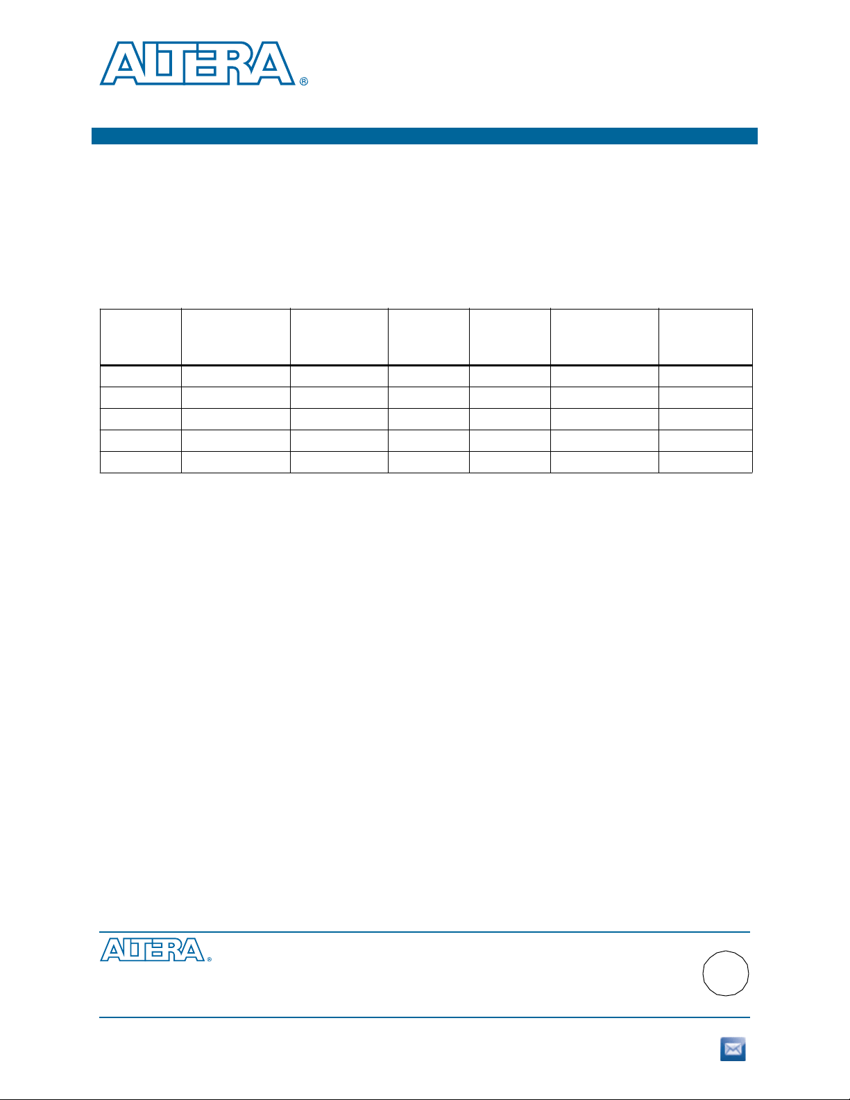
Figure 1 shows the EPCS device block diagram.
Figur e 1. EPCS Device Bl ock Diagram
EPCS Device
nCS
DCLK
Control
Logic
Decode Logic
Accessing Memory in EPCS Devices
You can access the unused memory locations of the EPCS device to store or retrieve
data through the Nios processor and SOPC Builder. SOPC Builder is an Altera tool for
creating bus-based (especially microprocessor-based) systems in Altera devices.
SOPC Builder assembles library components such as processors and memories into
custom microprocessor systems.
I/O Shift
Register
Data Buffer
Memory
Array
DATA
ASDI
Status RegisterAddress Counter
SOPC Builder includes the EPCS device controller core, which is an interface core
designed specifically to work with the EPCS device. With this core, you can create a
system with a Nios embedded processor that allows software access to any memory
location within the EPCS device.
Active Serial FPGA Configuration
The following Altera FPGAs support the AS configuration scheme with EPCS devices:
■ Arria
■ Cyclone
■ All device families in the Stratix
There are four signals on the EPCS device that interface directly with the FPGA’s
control signals. The EPCS device signals are
the
1 For more information about the EPCS device pin description, refer to Table 22 on
page 36.
series
series
DATA0, DCLK, ASDO
, and
nCSO
series except the Stratix device family
DATA, DCLK, ASDI
, and
nCS
interface with
control signals on the FPGA, respectively.
Serial Configuration (EPCS) Devices DatasheetJanuary 2012 Altera Corporation
Page 4
Page 4 Active Serial FPGA Configuration
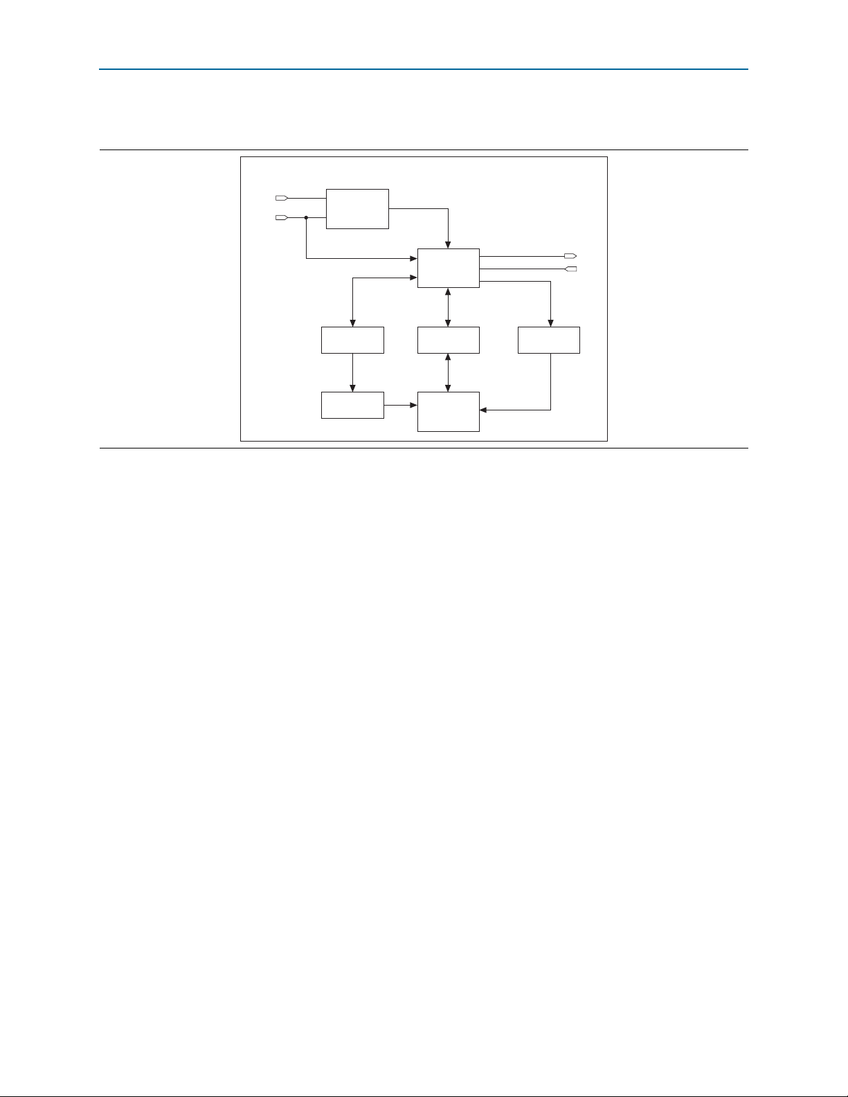
Figure 2 shows the configuration of an FPGA device in the AS configuration scheme
with an EPCS device using a download cable.
Figur e 2. Alt era FPGA Configuration in AS Mode Using a Download Cable
VCC (1) VCC (1) VCC (1)
10 kΩ 10 kΩ 10 kΩ
CONF_DONE
nSTATUS
nCONFIG
EPCS Device (2)
nCE
10 kΩ
DATA
DCLK
nCS
ASDI
Pin 1
DATA0
DCLK
nCSO
ASDO
V
(1)
CC
(1), (4)
Altera FPGA
nCEO
MSEL[]
N.C.
(3)
Notes to Figure 2:
(1) For more information about the VCC value, refer to the configuration chapter in the appropriate device handbook.
(2) EPCS devices cannot be cascaded.
(3) Connect the
MSEL[]
input pins to select the AS configuration mode. For more information, refer to the configuration chapter in the appropriate
device handbook.
(4) For more information about configuration pin I/O requirements in an AS configuration scheme for an Altera FPGA, refer to the configuration
chapter in the appropriate device handbook.
Serial Configuration (EPCS) Devices Datasheet January 2012 Altera Corporation
Page 5
Active Serial FPGA Configuration Page 5
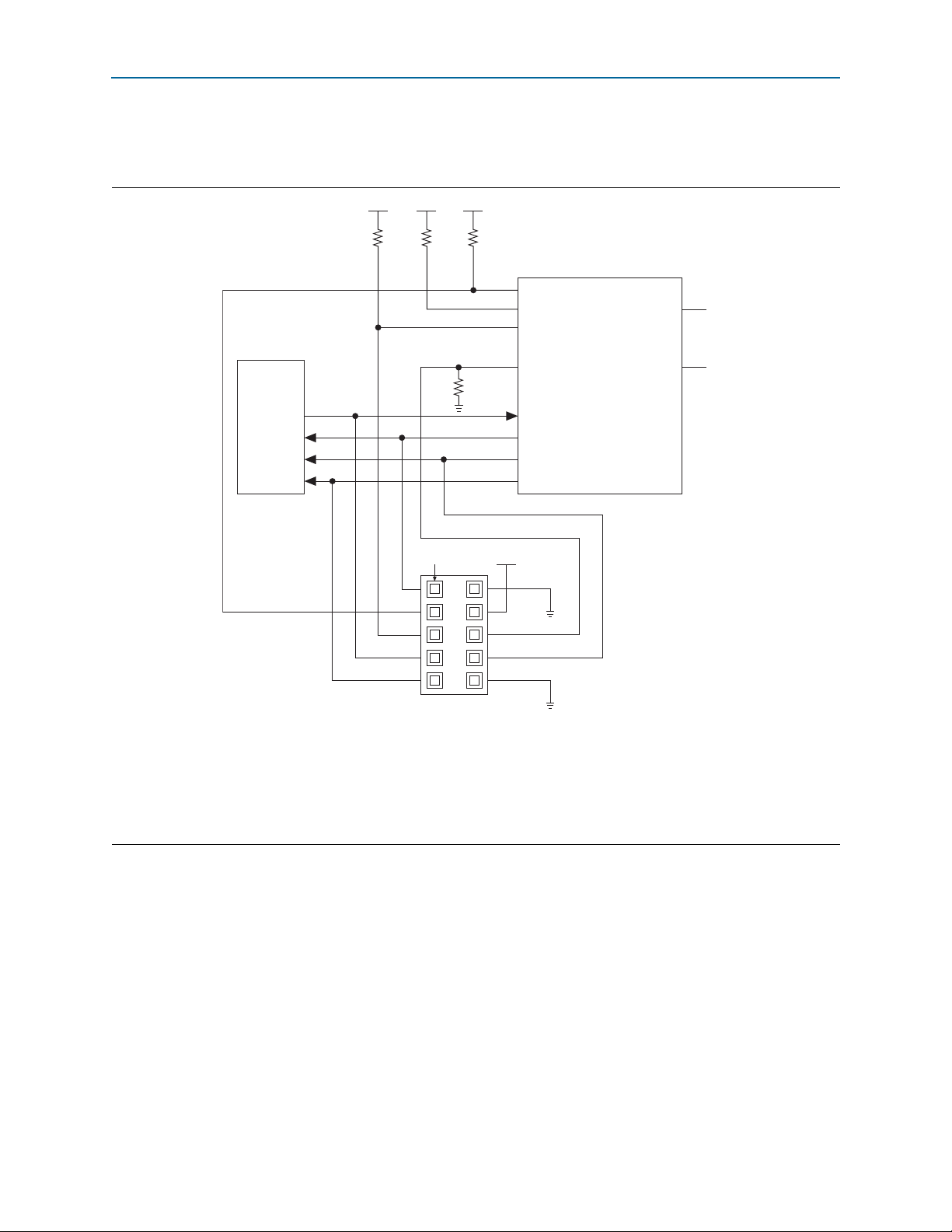
Figure 3 shows the configuration of an FPGA device in the AS configuration scheme
with an EPCS device using the APU or a third-party programmer.
Figur e 3. Alt era FPGA Configuration in AS Mode Usin g APU or a Thir d-party Programmer
VCC (1) VCC (1) VCC (1)
10 kΩ 10 kΩ 10 kΩ
Altera FPGA
CONF_DONE
nSTATUS
nCONFIG
EPCS Device (2)
nCE
DATA
DCLK
nCS
ASDI
Notes to Figure 3:
(1) For more information about the VCC value, refer to the configuration chapter in the appropriate device handbook.
(2) EPCS devices cannot be cascaded.
(3) Connect the
device handbook.
(4) For more information about configuration pin I/O requirements in an AS configuration scheme for an Altera FPGA, refer to the configuration
chapter in the appropriate device handbook.
MSEL[]
input pins to select the AS configuration mode. For more information, refer to the configuration chapter in the appropriate
DATA0
DCLK
nCSO
ASDO
(1) , (4)
nCEO
MSEL[]
N.C.
(3)
In an AS configuration, the FPGA acts as the configuration master in the
configuration flow and provides the clock to the EPCS device. The FPGA enables the
EPCS device by pulling the
nCS
signal low using the
nCSO
signal as shown in Figure 2
and Figure 3. Then, the FPGA sends the instructions and addresses to the EPCS device
using the
configuration data to the FPGA’s
latched into the FPGA on the next
ASDO
signal. The EPCS device responds to the instructions by sending the
DATA0
pin on the falling edge of
DCLK
signal’s falling edge.
DCLK
. The data is
1 Before the FPGA enters configuration mode, ensure that VCC of the EPCS device is
ready. If VCC is not ready, you must hold
nCONFIG
low until all power rails of EPCS
device are ready.
The FPGA controls the
mode. If the
CONF_DONE
signal goes high too early, the FPGA pulses its
reconfiguration. If the configuration is successful, the FPGA releases the
pin, allowing the external 10-k resistor to pull the
initialization begins after the
nSTATUS
and
CONF_DONE
pins during configuration in the AS
signal does not go high at the end of configuration, or if the
nSTATUS
pin low to start a
CONF_DONE
CONF_DONE
CONF_DONE
pin goes high. After the initialization, the
signal high. The FPGA
FPGA enters user mode.
f For more information about configuring the FPGAs in AS configuration mode or
other configuration modes, refer to the configuration chapter in the appropriate
device handbook.
Serial Configuration (EPCS) Devices DatasheetJanuary 2012 Altera Corporation
Page 6

Page 6 Active Serial FPGA Configuration
DATA
DCLK
nCS
ASDI
DATA0
DCLK
nCSO
nCE
nCONFIG
nSTATUS
MSEL[ ]
nCEO
CONF_DONE
ASDO
VCC (1)
10 kΩ
VCC (1)
10 kΩ
VCC (1)
10 kΩ
(3)
Altera FPGA (Master)
DATA0
DCLK
nCE
nCONFIG
nSTATUS
MSEL[ ]
nCEO
CONF_DONE
(4)
Altera FPGA (Slave)
EPCS Device (2)
N.C.
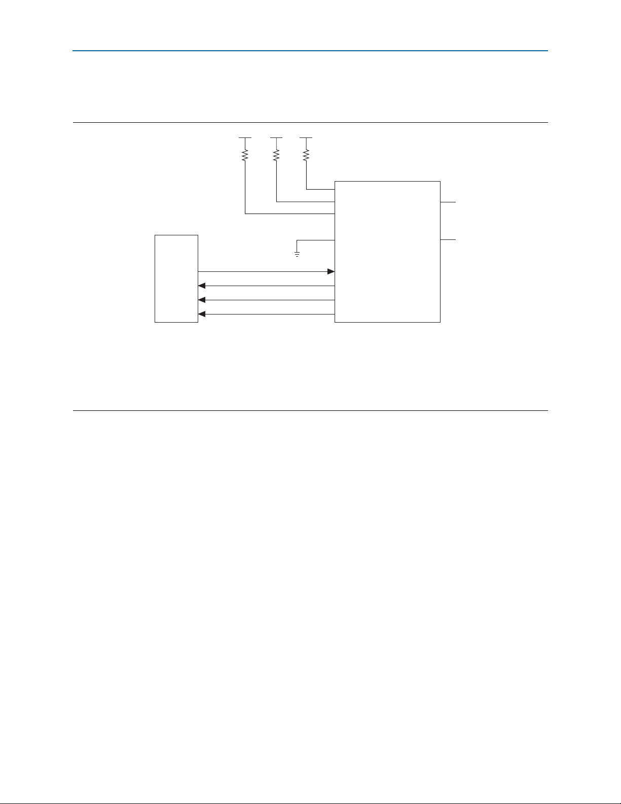
You can configure multiple devices with a single EPCS device. However, you cannot
cascade EPCS devices. To ensure that the programming file size of the cascaded
FPGAs does not exceed the capacity of an EPCS device, refer to Table 1 on page 1.
Figure 4 shows the AS configuration scheme with multiple FPGAs in the chain. The
first FPGA is the configuration master and its
following FPGAs are configuration slave devices and their
MSEL[]
pins are set to AS mode. The
MSEL[]
pins are set to PS
mode.
Figure 4. Multiple Devices in AS Mode
(1), (5)
Notes to Figure 4:
(1) For more information about the VCC value, refer to the configuration chapter in the appropriate device handbook.
(2) EPCS devices cannot be cascaded.
(3) Connect the
MSEL[]
input pins to select the AS configuration mode. For more information, refer to the configuration chapter in the appropriate
device handbook.
(4) Connect the
MSEL[]
input pins to select the PS configuration mode. For more information, refer to the configuration chapter in the appropriate
device handbook.
(5) For more information about configuration pin I/O requirements in an AS configuration scheme for an Altera FPGA, refer to the configuration
chapter in the appropriate device handbook.
Serial Configuration (EPCS) Devices Datasheet January 2012 Altera Corporation
Page 7

EPCS Device Memory Access Page 7
EPCS Device Memory Access
This section describes the memory array organization and operation codes of the
EPCS device. For the timing specifications, refer to “Timing Information” on page 29.
Memory Array Organization
Ta b l e 2 lists the memory array organization details in EPCS128, EPCS64, EPCS16,
EPCS4, and EPCS1 devices.
Table 2. Memory Ar ray Organizat ion in EPCS Devices
Details EPCS128 EPCS64 EPCS16 EPCS4 EPCS1
Bytes
Number of sect ors 64 128 32 8 4
Bytes per sector
Pages per sector 1,024 256 256 256 128
Total number of
pages
Bytes per page 256 bytes 256 bytes 256 bytes 256 bytes 256 bytes
16,777,216 bytes
(128 Mb)
262,144 by tes
(2 Mb)
65,536 32,768 8,192 2,048 512
8,388,608 bytes
(64 Mb)
65,536 bytes
(512 Kb)
2,097,152 bytes
(16 Mb)
65,536 bytes
(512 Kb)
524,288 bytes
(4 Mb)
65,536 bytes
(512 Kb)
131,072 bytes
(1 Mb)
32,768 bytes
(256 Kb)
Ta b l e 3 through Table 7 on page 15 list the address range for each sector in EPCS128,
EPCS64, EPCS16, EPCS4, and EPCS1 devices.
Table 3. Address Range for Sectors in EPCS128 Devices (Part 1 of 3)
Sector
63
62
61
60
59
58
57
56
55
54
53
52
51
50
49
48
47
Address Range (Byte Addresses in HEX)
Start End
H'FC0000 H'FFFFFF
H'F80000 H'FBFFFF
H'F40000 H'F7FFFF
H'F00000 H'F3FFFF
H'EC0000 H'EFFFFF
H'E80000 H'EBFFFF
H'E40000 H'E7FFFF
H'E00000 H'E3FFFF
H'DC0000 H'DFFFFF
H'D80000 H'DBFFFF
H'D40000 H'D7FFFF
H'D00000 H'D3FFFF
H'CC0000 H'CFFFFF
H'C80000 H'CBFFFF
H'C40000 H'C7FFFF
H'C00000 H'C3FFFF
H'BC0000 H'BFFFFF
Serial Configuration (EPCS) Devices DatasheetJanuary 2012 Altera Corporation
Page 8

Page 8 EPCS Device Memory Access
Table 3. Address Range for Sectors in EPCS128 Devices (Part 2 of 3)
Sector
46
45
44
43
42
41
40
39
38
37
36
35
34
33
32
31
30
29
28
27
26
25
24
23
22
21
20
19
18
17
16
15
14
13
12
11
10
9
Address Range (Byte Addresses in HEX)
Start End
H'B80000 H'BBFFFF
H'B40000 H'B7FFFF
H'B00000 H'B3FFFF
H'AC0000 H'AFFFFF
H'A80000 H'ABFFFF
H'A40000 H'A7FFFF
H'A00000 H'A3FFFF
H'9C0000 H'9FFFFF
H'980000 H'9BFFFF
H'940000 H'97FFFF
H'900000 H'93FFFF
H'8C0000 H'8FFFFF
H'880000 H'8BFFFF
H'840000 H'87FFFF
H'800000 H'83FFFF
H'7C0000 H'7FFFFF
H'780000 H'7BFFFF
H'740000 H'77FFFF
H'700000 H'73FFFF
H'6C0000 H'6FFFFF
H'680000 H'6BFFFF
H'640000 H'67FFFF
H'600000 H'63FFFF
H'5C0000 H'5FFFFF
H'580000 H'5BFFFF
H'540000 H'57FFFF
H'500000 H'53FFFF
H'4C0000 H'4FFFFF
H'480000 H'4BFFFF
H'440000 H'47FFFF
H'400000 H'43FFFF
H'3C0000 H'3FFFFF
H'380000 H'3BFFFF
H'340000 H'37FFFF
H'300000 H'33FFFF
H'2C0000 H'2FFFFF
H'280000 H'2BFFFF
H'240000 H'27FFFF
Serial Configuration (EPCS) Devices Datasheet January 2012 Altera Corporation
Page 9

EPCS Device Memory Access Page 9
Table 3. Address Range for Sectors in EPCS128 Devices (Part 3 of 3)
Sector
8
7
6
5
4
3
2
1
0
Address Range (Byte Addresses in HEX)
Start End
H'200000 H'23FFFF
H'1C0000 H'1FFFFF
H'180000 H'1BFFFF
H'140000 H'17FFFF
H'100000 H'13FFFF
H'0C0000 H'0FFFFF
H'080000 H'0BFFFF
H'040000 H'07FFFF
H'000000 H'03FFFF
Serial Configuration (EPCS) Devices DatasheetJanuary 2012 Altera Corporation
Page 10

Page 10 EPCS Device Memory Access
Table 4. Address Range for Sectors in EPCS64 Devices (Part 1 of 4)
Sector
127
126
125
124
123
122
121
120
119
118
117
116
115
114
113
112
111
110
109
108
107
106
105
104
103
102
101
100
99
98
97
96
95
94
93
92
91
90
Address Range (Byte Addresses in HEX)
Start End
H'7F0000 H'7FFFFF
H'7E0000 H'7EFFFF
H'7D0000 H'7DFFFF
H'7C0000 H'7CFFFF
H'7B0000 H'7BFFFF
H'7A0000 H'7AFFFF
H'790000 H'79FFFF
H'780000 H'78FFFF
H'770000 H'77FFFF
H'760000 H'76FFFF
H'750000 H'75FFFF
H'740000 H'74FFFF
H'730000 H'73FFFF
H'720000 H'72FFFF
H'710000 H'71FFFF
H'700000 H'70FFFF
H'6F0000 H'6FFFFF
H'6E0000 H'6EFFFF
H'6D0000 H'6DFFFF
H'6C0000 H'6CFFFF
H'6B0000 H'6BFFFF
H'6A0000 H'6AFFFF
H'690000 H'69FFFF
H'680000 H'68FFFF
H'670000 H'67FFFF
H'660000 H'66FFFF
H'650000 H'65FFFF
H'640000 H'64FFFF
H'630000 H'63FFFF
H'620000 H'62FFFF
H'610000 H'61FFFF
H'600000 H'60FFFF
H'5F0000 H'5FFFFF
H'5E0000 H'5EFFFF
H'5D0000 H'5DFFFF
H'5C0000 H'5CFFFF
H'5B0000 H'5BFFFF
H'5A0000 H'5AFFFF
Serial Configuration (EPCS) Devices Datasheet January 2012 Altera Corporation
Page 11

EPCS Device Memory Access Page 11
Table 4. Address Range for Sectors in EPCS64 Devices (Part 2 of 4)
Sector
89
88
87
86
85
84
83
82
81
80
79
78
77
76
75
74
73
72
71
70
69
68
67
66
65
64
63
62
61
60
59
58
57
56
55
54
53
52
Address Range (Byte Addresses in HEX)
Start End
H'590000 H'59FFFF
H'580000 H'58FFFF
H'570000 H'57FFFF
H'560000 H'56FFFF
H'550000 H'55FFFF
H'540000 H'54FFFF
H'530000 H'53FFFF
H'520000 H'52FFFF
H'510000 H'51FFFF
H'500000 H'50FFFF
H'4F0000 H'4FFFFF
H'4E0000 H'4EFFFF
H'4D0000 H'4DFFFF
H'4C0000 H'4CFFFF
H'4B0000 H'4BFFFF
H'4A0000 H'4AFFFF
H'490000 H'49FFFF
H'480000 H'48FFFF
H'470000 H'47FFFF
H'460000 H'46FFFF
H'450000 H'45FFFF
H'440000 H'44FFFF
H'430000 H'43FFFF
H'420000 H'42FFFF
H'410000 H'41FFFF
H'400000 H'40FFFF
H'3F0000 H'3FFFFF
H'3E0000 H'3EFFFF
H'3D0000 H'3DFFFF
H'3C0000 H'3CFFFF
H'3B0000 H'3BFFFF
H'3A0000 H'3AFFFF
H'390000 H'39FFFF
H'380000 H'38FFFF
H'370000 H'37FFFF
H'360000 H'36FFFF
H'350000 H'35FFFF
H'340000 H'34FFFF
Serial Configuration (EPCS) Devices DatasheetJanuary 2012 Altera Corporation
Page 12

Page 12 EPCS Device Memory Access
Table 4. Address Range for Sectors in EPCS64 Devices (Part 3 of 4)
Sector
51
50
49
48
47
46
45
44
43
42
41
40
39
38
37
36
35
34
33
32
31
30
29
28
27
26
25
24
23
22
21
20
19
18
17
16
15
14
Address Range (Byte Addresses in HEX)
Start End
H'330000 H'33FFFF
H'320000 H'32FFFF
H'310000 H'31FFFF
H'300000 H'30FFFF
H'2F0000 H'2FFFFF
H'2E0000 H'2EFFFF
H'2D0000 H'2DFFFF
H'2C0000 H'2CFFFF
H'2B0000 H'2BFFFF
H'2A0000 H'2AFFFF
H'290000 H'29FFFF
H'280000 H'28FFFF
H'270000 H'27FFFF
H'260000 H'26FFFF
H'250000 H'25FFFF
H'240000 H'24FFFF
H'230000 H'23FFFF
H'220000 H'22FFFF
H'210000 H'21FFFF
H'200000 H'20FFFF
H'1F0000 H'1FFFFF
H'1E0000 H'1EFFFF
H'1D0000 H'1DFFFF
H'1C0000 H'1CFFFF
H'1B0000 H'1BFFFF
H'1A0000 H'1AFFFF
H'190000 H'19FFFF
H'180000 H'18FFFF
H'170000 H'17FFFF
H'160000 H'16FFFF
H'150000 H'15FFFF
H'140000 H'14FFFF
H'130000 H'13FFFF
H'120000 H'12FFFF
H'110000 H'11FFFF
H'100000 H'10FFFF
H'0F0000 H'0FFFFF
H'0E0000 H'0EFFFF
Serial Configuration (EPCS) Devices Datasheet January 2012 Altera Corporation
Page 13

EPCS Device Memory Access Page 13
Table 4. Address Range for Sectors in EPCS64 Devices (Part 4 of 4)
Sector
13
12
11
10
9
8
7
6
5
4
3
2
1
0
Address Range (Byte Addresses in HEX)
Start End
H'0D0000 H'0DFFFF
H'0C0000 H'0CFFFF
H'0B0000 H'0BFFFF
H'0A0000 H'0AFFFF
H'090000 H'09FFFF
H'080000 H'08FFFF
H'070000 H'07FFFF
H'060000 H'06FFFF
H'050000 H'05FFFF
H'040000 H'04FFFF
H'030000 H'03FFFF
H'020000 H'02FFFF
H'010000 H'01FFFF
H'000000 H'00FFFF
Serial Configuration (EPCS) Devices DatasheetJanuary 2012 Altera Corporation
Page 14

Page 14 EPCS Device Memory Access
Table 5. Address Range for Sectors in EPCS16 Devi ces
Sector
31
30
29
28
27
26
25
24
23
22
21
20
19
18
17
16
15
14
13
12
11
10
9
8
7
6
5
4
3
2
1
0
Address Range (Byte Addresses in HEX)
Start End
H'1F0000 H'1FFFFF
H'1E0000 H'1EFFFF
H'1D0000 H'1DFFFF
H'1C0000 H'1CFFFF
H'1B0000 H'1BFFFF
H'1A0000 H'1AFFFF
H'190000 H'19FFFF
H'180000 H'18FFFF
H'170000 H'17FFFF
H'160000 H'16FFFF
H'150000 H'15FFFF
H'140000 H'14FFFF
H'130000 H'13FFFF
H'120000 H'12FFFF
H'110000 H'11FFFF
H'100000 H'10FFFF
H'0F0000 H'0FFFFF
H'0E0000 H'0EFFFF
H'0D0000 H'0DFFFF
H'0C0000 H'0CFFFF
H'0B0000 H'0BFFFF
H'0A0000 H'0AFFFF
H'090000 H'09FFFF
H'080000 H'08FFFF
H'070000 H'07FFFF
H'060000 H'06FFFF
H'050000 H'05FFFF
H'040000 H'04FFFF
H'030000 H'03FFFF
H'020000 H'02FFFF
H'010000 H'01FFFF
H'000000 H'00FFFF
Serial Configuration (EPCS) Devices Datasheet January 2012 Altera Corporation
Page 15

EPCS Device Memory Access Page 15
Table 6. Address Range for Sectors in EPCS4 Devices
Sector
7
6
5
4
3
2
1
0
Table 7. Address Range for Sectors in EPCS1 Devices
Sector
3
2
1
0
Address Range (Byte Addresses in HEX)
Start End
H'70000 H'7FFFF
H'60000 H'6FFFF
H'50000 H'5FFFF
H'40000 H'4FFFF
H'30000 H'3FFFF
H'20000 H'2FFFF
H'10000 H'1FFFF
H'00000 H'0FFFF
Address Range (Byte Addresses in HEX)
Start End
H'18000 H'1FFFF
H'10000 H'17FFF
H'08000 H'0FFFF
H'00000 H'07FFF
Operation Codes
This section describes the operations that you can use to access the memory in EPCS
devices. Use the
devices. When performing the operation, addresses and data are shifted in and out of
the device serially, with MSB first.
The device samples the AS data input on the first rising edge of the
active low chip select (
MSB first, into the EPCS device serially through the AS data input (
operation code bit is latched into the EPCS device on the rising edge of the
Different operations require a different sequence of inputs. While executing an
operation, you must shift in the desired operation code, followed by the address bytes
or data bytes, both address and data bytes, or none of them. The device must drive
nCS
pin high after the last bit of the operation sequence is shifted in. Tab l e 8 lists the
operation sequence for every operation supported by the EPCS devices.
For read operations, the data read is shifted out on the
pin high after any bit of the data-out sequence is shifted out.
For write and erase operations, drive the
multiple of eight clock pulses. Otherwise, the operation is rejected and not executed.
DATA, DCLK, ASDI
nCS
) input signal is driven low. Shift the operation code, with
, and
nCS
signals to access the memory in EPCS
DCLK
ASDI
DATA
pin. You can drive the
nCS
pin high at a byte boundary that is in a
after the
) pin. Each
DCLK
.
nCS
Serial Configuration (EPCS) Devices DatasheetJanuary 2012 Altera Corporation
Page 16
Page 16 EPCS Device Memory Access
nCS
DCLK
ASDI
DATA
01234567
Operation Code
High Impedance
All attempts to access the memory contents while a write or erase cycle is in progress
are rejected, and the write or erase cycle will continue unaffected.
Table 8. EPCS Devices Operation Codes
(1)
Operation Operation Code
Write enable
Write disable
Read status
Read bytes
Read silicon ID
(4)
Fast read
Write status
Write bytes
Erase bulk
Erase sector
Read device
identification
Notes to Tab le 8 :
(1) List MSB first and LSB last.
(2) The status register, data, or silicon ID is read out at least once on the
(3) A write bytes operation requires a t least one data byte on the
are written to the memory.
(4) The read silicon ID operation is available only for EPCS1, EPCS4, EPCS16, and EPCS64 devices.
(5) The read device identification operation is available only for EPCS128 devices.
(5)
0000 0110
0000 0100
0000 0101
0000 0011
1010 1011
0000 1011
0000 0001
0000 0010
1100 0111
1101 1000
1001 1111 0 2 1 to infinite
Address Bytes Dummy Bytes Data Bytes
00 025
00 025
0 0 1 to infinite
3 0 1 to infinite
0 3 1 to infinite
3 1 1 to infinite
00 125
3 0 1 to 256
00 025
30 025
DATA
pin and is continuously read out until the
DATA
pin. If more than 256 bytes are sent to the device, only the last 256 bytes
(2)
(2)
(2)
(2)
(3)
(2)
nCS
pin is driven high.
DCLK f
(MHz)
25
20
25
40
25
25
MAX
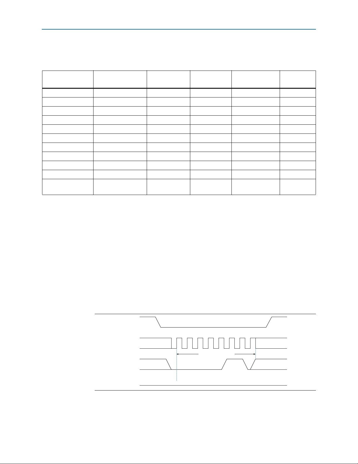
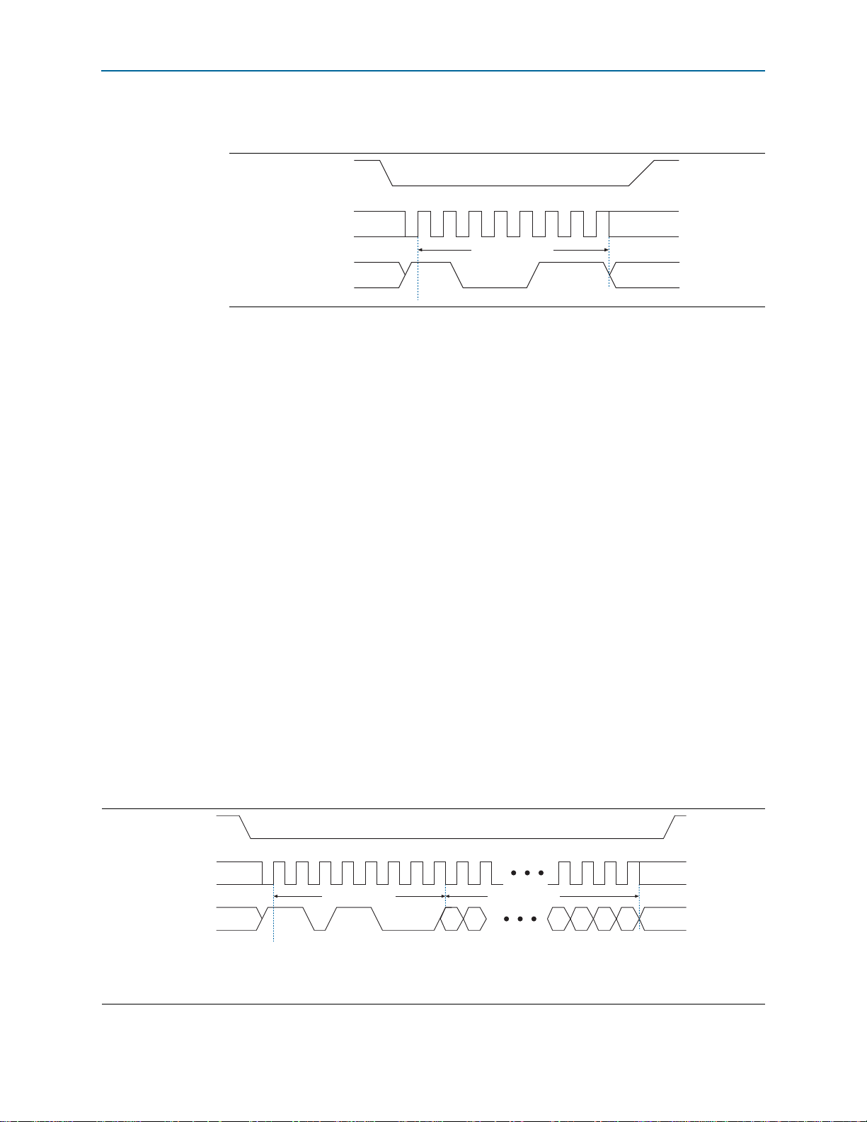
Write Enable Operation
The write enable operation code is
enable operation sets the write enable latch bit, which is bit 1 in the status register.
Always set the write enable latch bit before write bytes, write status, erase bulk, and
erase sector operations. Figure 5 shows the instruction sequence of the write enable
operation.
Figur e 5. Write Enabl e Operation Timing Diagram
b'0000 0110
, and it lists the MSB first. The write
Serial Configuration (EPCS) Devices Datasheet January 2012 Altera Corporation
Page 17

EPCS Device Memory Access Page 17
nCS
DCLK
ASDI
DATA
01234567
Operation Code
High Impedance
Write Disable Operation
The write disable operation code is
disable operation resets the write enable latch bit, which is bit1 in the status register.
To prevent the memory from being written unintentionally, the write enable latch bit
is automatically reset when implementing the write disable operation, and under the
following conditions:
■ Power up
■ Write bytes operation completion
■ Write status operation completion
■ Erase bulk operation completion
■ Erase sector operation completion
Figure 6 shows the instruction sequence of the write disable operation.
Figur e 6. Write Disable Operation Timing Di agram
b'0000 0100
and it lists the MSB first. The write
Serial Configuration (EPCS) Devices DatasheetJanuary 2012 Altera Corporation
Page 18

Page 18 EPCS Device Memory Access
Bit 7 Bit 0
Block Protect Bits [2..0]
Write In
Progress Bit
Write Enable
Latch Bit
BP2 BP1 BP0 WEL WIP
Bit 7 Bit 0
Block Protect
Bits [1..0]
Write In
Progress Bit
Write Enable
Latch Bit
BP1 BP0 WEL WIP
Read Status Operation
The read status operation code is
the read status operation to read the status register. Figure 7 and Figure 8 show the
status bits in the status register of the EPCS devices.
Figure 7. EPCS128, EPCS64, EPCS16, and EPCS4 Status Register Status Bits
Figur e 8. E PCS1 Statu s Register Status Bits
b'0000 0101
and it lists the MSB first. You can use
Setting the write in progress bit to 1 indicates that the EPCS device is busy with a
write or erase cycle. Resetting the write in progress bit to 0 indicates no write or erase
cycle is in progress.
Resetting the write enable latch bit to 0 indicates that no write or erase cycle is
accepted. Set the write enable latch bit to 1 before every write bytes, write status, erase
bulk, and erase sector operations.
The non-volatile block protect bits determine the area of the memory protected from
being written or erased unintentionally. Table 9 through Table 12 on page 20 list the
protected area in the EPCS devices with reference to the block protect bits. The erase
bulk operation is only available when all the block protect bits are set to 0. When any
of the block protect bits are set to 1, the relevant area is protected from being written
by a write bytes operation or erased by an erase sector operation.
Serial Configuration (EPCS) Devices Datasheet January 2012 Altera Corporation
Page 19

EPCS Device Memory Access Page 19
Table 9. Block Protection Bits in the EPCS1 Device
Status Register Content Memory Content
BP1 Bit BP0 Bit Protected Area Unprotected Area
00
01
10
11
None All four sectors—0 to 3
Sector 3 Three sectors—0 to 2
Two sectors—2 and 3 Two sectors—0 and 1
All sectors None
Table 10. Block Protection Bits in the EPCS4 Device
Stat us Regis ter Content Memory Content
BP2 Bit BP1 Bit BP0 Bit Protected Area Unprotected Area
000
001
010
011
100
101
110
111
None All eight s ectors—0 to 7
Sector 7 Seven sectors—0 to 6
Sectors 6 and 7 Six sectors—0 to 5
Four sectors—4 to 7 Four sectors—0 to 3
All sectors None
All sectors None
All sectors None
All sectors None
Table 11. Block Protection Bits in the EPCS16 Device
Status Register
Content
BP2
BP1
BP0
Bit
Bit
Bit
000
001
010
011
100
101
110
111
None All sectors (32 sectors 0 to 31)
Upper 32nd (Sector 31) Lower 31/32nds (31 sect ors—0 to 30)
Upper sixteenth (two sectors—30 and 31) Lower 15/16ths (30 sectors—0 to 29)
Upper eighth (four sectors—28 to 31) Lower seven-eighths (28 sectors—0 to 27)
Upper quarter (eight sectors—24 to 31) Lower three-quarters (24 sectors—0 to 23)
Upper half (sixteen sectors—16 to 31) Lower half (16 sectors—0 to 15)
All sectors (32 sectors—0 to 31) None
All sectors (32 sectors—0 to 31) None
Protected Area Unprotected Area
Memory Content
Serial Configuration (EPCS) Devices DatasheetJanuary 2012 Altera Corporation
Page 20
Page 20 EPCS Device Memory Access
nCS
DCLK
ASDI
DATA
0 1 2 3 4 5 6 7 8 9 101112131415
765432107 21076543
Operation Code
MSB MSB
Status Register Out Status Register Out
High Impedance
Table 12. Block Protection Bits in the EPCS128 Device
Statu s Register
Content
BP2
BP1
BP0
Bit
Bit
Bit
000
001
010
011
100
101
110
111
None All sectors (64 sectors—0 to 63)
Upper 64th (1 sector—63) Lower 63/64ths (63 sectors—0 to 62)
Upper 32nd (2 sectors—62 to 63) Lower 31/32nds (62 sectors—0 to 61)
Upper 16th (4 sectors—60 to 63) Lower 15/16ths (60 sec tors—0 to 59)
Upper 8th (8 sectors—56 to 63) Lower seven-eighths (56 sectors—0 to 55)
Upper quarter (16 sectors—48 to 63) Lower three-quarters (48 sectors—0 to 47)
Upper half (32 sectors—32 to 63) Lower half (32 sectors—0 to 31)
All sectors (64 sectors—0 to 63) None
Protected Area Unprotected Ar ea
You can read the status register at any time, even during a write or erase cycle is in
progress. When one of these cycles is in progress, you can check the write in progress
bit (bit 0 of the status register) before sending a new operation to the device. The
device can also read the status register continuously, as shown in Figure 9.
Figur e 9. Read Status Operation Timing Diagram
Memory Content
Write Status Operation
The write status operation code is
status operation to set the status register block protection bits. The write status
operation does not affect the other bits. Therefore, you can implement this operation
to protect certain memory sectors, as listed in Table 9 through Tab l e 1 2 . After setting
the block protect bits, the protected memory sectors are treated as read-only memory.
You must execute the write enable operation before the write status operation so the
device sets the status register’s write enable latch bit to 1.
The write status operation is implemented by driving the
shifting in the write status operation code and one data byte for the status register on
the
ASDI
pin. Figure 10 shows the instruction sequence of the write status operation.
The
nCS
must be driven high after the eighth bit of the data byte has been latched in,
otherwise the write status operation is not executed.
Serial Configuration (EPCS) Devices Datasheet January 2012 Altera Corporation
b'0000 0001
and it lists the MSB first. Use the write
nCS
signal low, followed by
Page 21
EPCS Device Memory Access Page 21
nCS
DCLK
ASDI
DATA
0123456789101112131415
Operation Code Status Register
76543210
MSB
High Impedance
Immediately after the
status cycle. The self-timed write status cycle usually takes 5 ms for all EPCS devices
and is guaranteed to be less than 15 ms. For more information, refer to the tWS value in
Table 15 on page 29. You must account for this delay to ensure that the status register
is written with desired block protect bits. Alternatively, you can check the write in
progress bit in the status register by executing the read status operation while the
self-timed write status cycle is in progress. The write in progress bit is 1 during the
self-timed write status cycle and 0 when it is complete.
Figur e 10. Write Status Operation Timing Di agram
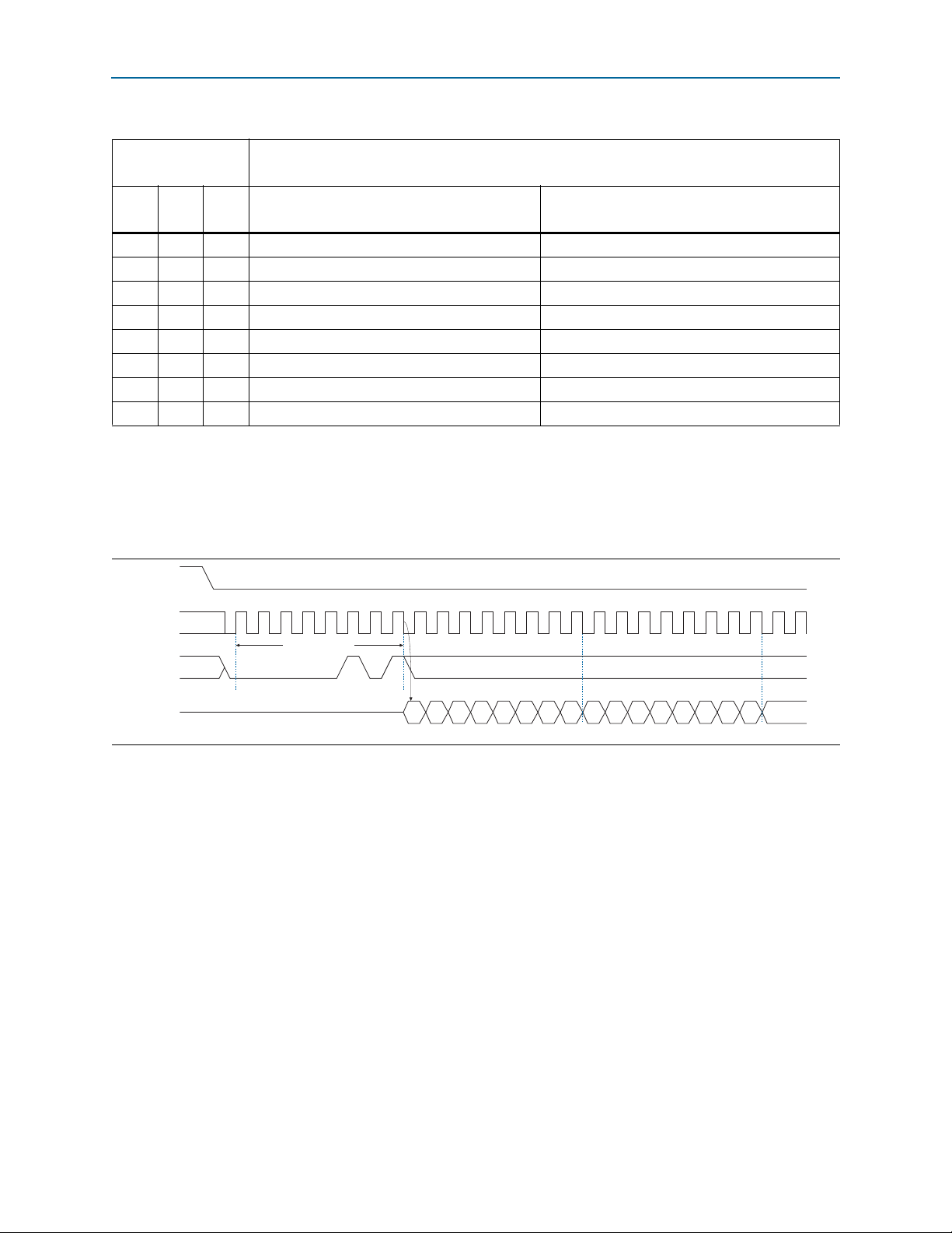
Read Bytes Operation
The read bytes operation code is
memory contents of the EPCS device, the device is first selected by driving the
signal low. Then, the read bytes operation code is shifted in followed by a 3-byte
address (
signal. After the address is latched in, the memory contents of the specified address
are shifted out serially on the
Programming Data files (.rpd), the content is shifted out serially beginning with the
LSB. Each data bit is shifted out on the falling edge of the
DCLK
A[23..0]
). Each address bit must be latched in on the rising edge of the
frequency during the read bytes operation is 20 MHz.
nCS
signal drives high, the device initiates the self-timed write
b'0000 0011
DATA
pin, beginning with the MSB. For reading Raw
and it lists the MSB first. To read the
DCLK
signal. The maximum
nCS
DCLK
The first byte address can be at any location. The device automatically increases the
address to the next higher address after shifting out each byte of data. Therefore, the
device can read the whole memory with a single read bytes operation. When the
device reaches the highest address, the address counter restarts at
the memory contents to be read out indefinitely until the read bytes operation is
terminated by driving the
nCS
signal high. The device can drive the
any time after data is shifted out. If the read bytes operation is shifted in while a write
or erase cycle is in progress, the operation is not executed and does not affect the write
or erase cycle in progress.
0x000000
nCS
Serial Configuration (EPCS) Devices DatasheetJanuary 2012 Altera Corporation
, allowing
signal high at
Page 22
Page 22 EPCS Device Memory Access
nCS
DCLK
ASDI
DATA
0 1 2 3 4 5 6 7 8 9 10 28 29 30 31 32 33 34 35 36 37 38 39
Operation Code 24-Bit Address (1)
23 22 21 3 2 1 0
776543210
MSB
MSB (2)
High Impedance
DATA Out 1 DATA Out 2
Figure 11 shows the instruction sequence of the read bytes operation.
Figur e 11. Read Bytes Operation Timing Dia gram
Notes to Figure 11:
(1) Address bit
A[23..19]
(2) For .rpd files, the read sequence shifts out the LSB of the data byte first.
A[23]
is a don't-care bit in the EPCS64 device. Address bits
are don't-care bits in the EPCS4 device. Address bits
A[23..21 ]
A[23..17 ]
are don't-care bits in the EPCS16 device. Address bits
are don't-care bits in the EPCS1 device.
Fast Read Operation
The fast read operation code is
the device by driving the
a 3-byte address (
ris ing ed ge of t he
on
DATA
with each bit being shifted out at a maximum frequency of 40 MHz during
the falling edge of the
A23-A0
) and a dummy byte with each bit being latched-in during the
DCLK
signal. Then, the memory contents at that address is shifted out
DCLK
b’0000 1011
nCS
signal low. The fast read instruction code is followed by
and it lists the MSB first. You can select
signal.
The first addressed byte can be at any location. The address is automatically increased
to the next higher address after each byte of data is shifted out. Therefore, the whole
memory can be read with a single fast read instruction. When the highest address is
reached, the address counter rolls over to
000000h
, allowing the read sequence to
continue indefinitely.
The fast read instruction is terminated by driving the
nCS
signal high at any time
during data output. Any fast read instruction is rejected during the erase, program, or
write operations without affecting the operation that is in progress.
Serial Configuration (EPCS) Devices Datasheet January 2012 Altera Corporation
Page 23

EPCS Device Memory Access Page 23
Figure 12 shows the instruction sequence of the fast read operation.
Figur e 12. Fast Read Operation Timing Diagram
nCS
0 1 2 3 4 5 6 7 8 9 10 28 29 30 31
DCLK
Operation Code
ASDI
DATA
nCS
32 33 34 35 36 37 38 39 40 41 42 43 44 45 46 47
DCLK
ASDI
765432 0
DATA
High Impedance
Dummy Byte
1
765432 0
MSB MSB MSB
23 22 21 3 2 1 0
MSB
DATA Out 1 DATA Out 2
Note to Figure 12:
(1) Address bit
EPCS16 device. Address bits
don't-care bits in the EPCS1 device.
A[23]
is a don't-care bit in the EPCS64 device. Address bits
A[23..19]
are don't-care bits in the EPCS4 device. Address bits
24-Bit Address (1)
1
7 65432107
A[23..21 ]
are don't-care bits in the
A[23..17]
are
Read Silicon ID Operation
The read silicon ID operation code is
EPCS1, EPCS4, EPCS16, and EPCS64 devices support this operation. This operation
reads the 8-bit silicon ID of the EPCS device from the
is shifted in during an erase or write cycle, it is ignored and does not affect the cycle
that is in progress.
Ta b l e 1 3 lists the EPCS device silicon IDs.
Table 13. EPCS Devi ce Silicon ID
EPCS Device Silicon ID (Binary Value)
EPCS1
EPCS4
EPCS16
EPCS64
The device implements the read silicon ID operation by driving the
and then shifting in the read silicon ID operation code, followed by three dummy
bytes on the
DATA
pin on the falling edge of the
ASDI
pin. The 8-bit silicon ID of the EPCS device is then shifted out on the
silicon ID operation by driving the
one time. Sending additional clock cycles on
the silicon ID to be shifted out repeatedly.
b'1010 1011
and it lists the MSB first. Only
DATA
output pin. If this operation
b'0001 0000
b'0001 0010
b'0001 0100
b'0001 0110
nCS
signal low
DCLK
signal. The device can terminate the read
nCS
signal high after reading the silicon ID at least
DCLK
while
nCS
is driven low can cause
Serial Configuration (EPCS) Devices DatasheetJanuary 2012 Altera Corporation
Page 24

Page 24 EPCS Device Memory Access
nCS
DCLK
ASDI
DATA
0 1 2 3 4 5 6 7 8 9 10 28 29 30 31 32 33 34 35 36 37 38 39
Operation Code Three Dummy Bytes
23 22 21 3 2 1 0
76543210
MSB
MSB
High Impedance
Silicon ID
nCS
DCLK
ASDI
DATA
0 1 2 3 4 5 6 7 8 9 10 20 21 23 24 25 26 27 28 29 30 31 32
Operation Code Two Dummy Bytes
15
14 13
3210
76543210
MSB
MSB
High Impedance
Silicon ID
Figure 13 shows the instruction sequence of the read silicon ID operation.
Figur e 13. Read Silicon ID Operation Timing Diagram
(1)
Note to Figure 13:
(1) Only EPCS1, EPCS4, EPCS16, and EPCS64 devices support the read silicon ID operation.
Read Device Identification Operation
The read device identification operation code is
Only EPCS128 device supports this operation. This operation reads the 8-bit device
identification of the EPCS device from the
in during an erase or write cycle, it is ignored and does not affect the cycle that is in
progress. Ta ble 14 lists the EPCS device identification.
Table 14. EPCS Device Identification
EPCS Device Silicon ID (Binary Value)
EPCS128
DATA
b’1001 1111
and it lists the MSB first.
output pin. If this operation is shifted
b'0001 1000
The device implements the read device identification operation by driving the
signal low and then shifting in the read device identification operation code, followed
by two dummy bytes on the
device is then shifted out on the
device can terminate the read device identification operation by driving the
ASDI
pin. The 16-bit device identification of the EPCS
DATA
pin on the falling edge of the
DCLK
signal. The
nCS
high after reading the device identification at least one time.
Figure 14 shows the instruction sequence of the read device identification operation.
Figur e 14. Read Device Identification Operation Timing Diagram
Note to Figure 14:
(1) Only EPCS128 device supports the read device identification operation.
Serial Configuration (EPCS) Devices Datasheet January 2012 Altera Corporation
(1)
nCS
signal
Page 25

EPCS Device Memory Access Page 25
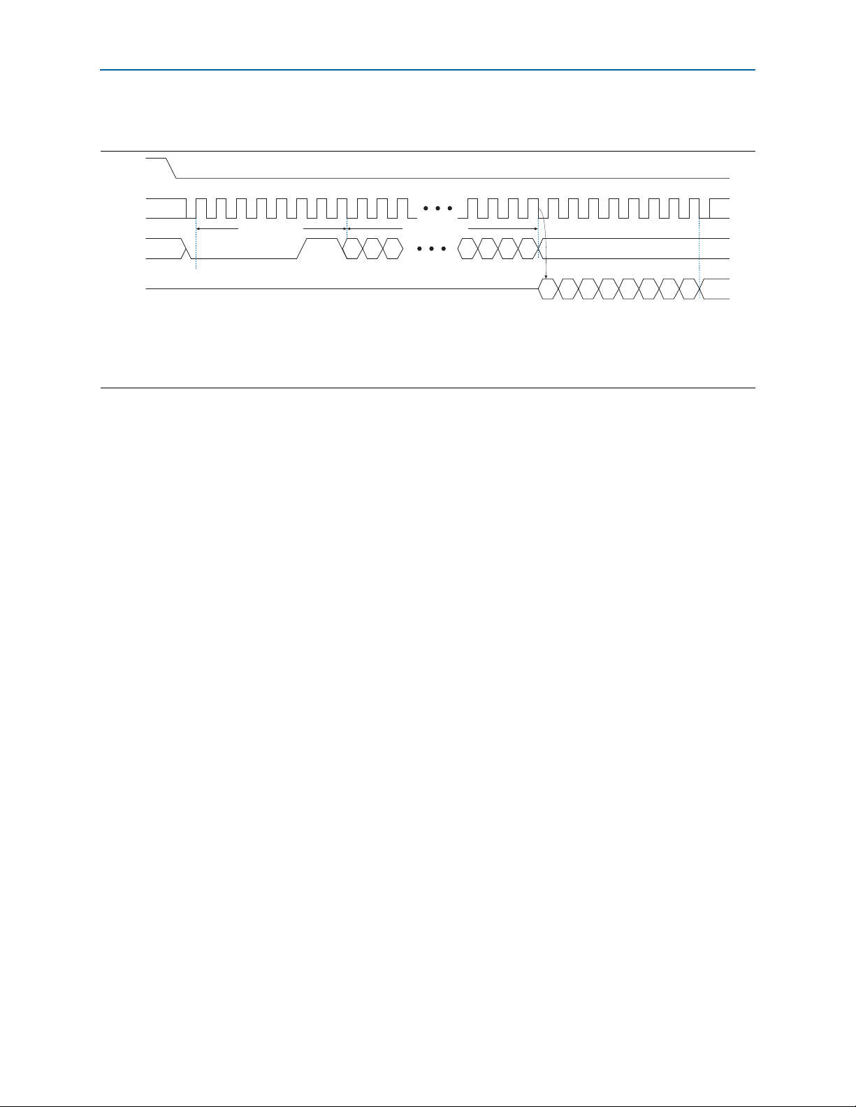
Write Bytes Operation
The write bytes operation code is
operation allows bytes to be written to the memory. You must execute the write enable
operation before the write bytes operation to set the write enable latch bit in the status
register to 1.
b'0000 0010
and it lists the MSB first. This
The write bytes operation is implemented by driving the
nCS
signal low, followed by
the write bytes operation code, three address bytes, and at least one data byte on the
ASDI
pin. If the eight LSBs (
A[7..0]
) are not all 0, all sent data that goes beyond the
end of the current page is not written into the next page. Instead, this data is written at
the start address of the same page (from the address whose eight LSBs are all 0). You
must ensure the
nCS
signal is set low during the entire write bytes operation.
If more than 256 data bytes are shifted into the EPCS device with a write bytes
operation, the previously latched data is discarded and the last 256 bytes are written
to the page. However, if less than 256 data bytes are shifted into the EPCS device, they
are guaranteed to be written at the specified addresses and the other bytes of the same
page are not affected.
If your design requires writing more than 256 data bytes to the memory, more than
one page of memory is required. Send the write enable and write bytes operation
codes, followed by three new targeted address bytes and 256 data bytes, before a new
page is written.
The
nCS
signal must be driven high after the eighth bit of the last data byte has been
latched in. Otherwise, the device does not execute the write bytes operation. The write
enable latch bit in the status register is reset to 0 before the completion of each write
bytes operation. Therefore, the write enable operation must be carried out before the
next write bytes operation.
The device initiates a self-timed write cycle immediately after the
nCS
signal is driven
high. For more information about the self-timed write cycle time, refer to the tWB value
in Table 15 on page 29. You must account for this amount of delay before another page
of memory is written. Alternatively, you can check the write in progress bit in the
status register by executing the read status operation while the self-timed write cycle
is in progress. The write in progress bit is set to 1 during the self-timed write cycle and
0
when it is complete.
1 You must erase all the memory bytes of the EPCS devices to all 1 or
implement the write bytes operation. You can erase all the memory bytes by executing
the erase sector operation in a sector or the erase bulk operation throughout the entire
memory.
Serial Configuration (EPCS) Devices DatasheetJanuary 2012 Altera Corporation
0xFF
before you
Page 26

Serial Configuration (EPCS) Devices Datasheet January 2012 Altera Corporation
Figure 15 shows the instruction sequence of the write bytes operation.
Page 26 EPCS Device Memory Access
Figure 15. Write Bytes Operation Timing Diagram
nCS
0 1 2 3 4 5 6 7 8 9 10 28 29 30 31 32 33 34 35 36 37 38 39 40 41 42 43 44 45 46 47 2072 2073 2074 2075 2076 2077 2078 2079
DCLK
Operation Code 24-Bit Address (2)
ASDI
23 22 21 3 2 1 0 7654
MSB MSB (3) MSB (3) MSB (3)
(1)
Data Byte 1 Data Byte 2 Data Byte 256
32107654 76543210 3210
Notes to Figu re 15:
(1) Use the erase sector operation or the erase bulk operation to initialize the memory bytes of the EPCS devices to all 1 or
(2) Address bit
bits
(3) For .rpd files, write the LSB of the data byte first.
A[23]
A[23..17]
is a don't-care bit in the EPCS64 device. Address bits
are don't-care bits in the EPCS1 device.
A[23..21]
are don't-care bits in the EPCS16 device. Address bi ts
Erase Bulk Operation
The erase bulk operation code is
Similar to the write bytes operation, you must execute the write enable operation before the erase bulk operation so that the
write enable latch bit in the status register is set to 1.
You can implement the erase bulk operation by driving the
the
ASDI
pin. The
nCS
signal must be driven high after the eighth bit of the erase bulk operation code has been latched in.
The device initiates a self-timed erase bulk cycle immediately after the
the self-timed erase bulk cycle time, refer to the tEB value in Table 15 on page 29.
b'1100 0111
and it lists the MSB first. This operation sets all the memory bits to 1 or
nCS
signal low and then shifting in the erase bulk operation code on
0xFF
before implementing the write bytes operation.
A[23..19]
nCS
signal is driven high. For more information about
are don't-care bit s in the EPCS4 device. Address
0xFF
.
You must account for this delay before accessing the memory contents. Alternatively, you can check the write in progress bit in
the status register by executing the read status operation while the self-timed erase cycle is in progress. The write in progress
bit is set to 1 during the self-timed erase cycle and 0 when it is complete. The write enable latch bit in the status register is reset
to 0 before the erase cycle is complete.
Page 27
EPCS Device Memory Access Page 27
nCS
DCLK
ASDI
01234567
Operation Code
Figure 16 shows the instruction sequence of the erase bulk operation.
Figur e 16. Erase Bulk Operation Timing Diagram
Erase Sector Operation
The erase sector operation code is
operation allows you to erase a certain sector in the EPCS device by setting all the bits
inside the sector to 1 or
0xFF
sectors as general purpose memory in your applications. You must execute the write
enable operation before the erase sector operation so that the write enable latch bit in
the status register is set to 1.
b'1101 1000
and it lists the MSB first. This
. This operation is useful if you want to access the unused
You can implement the erase sector operation by first driving the
you shift in the erase sector operation code, followed by the three address bytes of the
chosen sector on the
ASDI
can be any address inside the specified sector. For more information about the sector
address range, refer to Table 3 on page 7 through Table 7 on page 15. Drive the
signal high after the eighth bit of the erase sector operation code has been latched in.
The device initiates the self-timed erase sector cycle immediately after the
driven high. For more information about the self-timed erase sector cycle time, refer to
the tES value in Table 15 on page 29.
You must account for this delay before accessing the memory contents. Alternatively,
you can check the write in progress bit in the status register by executing the read
status operation while the self-timed erase sector cycle is in progress. The write in
progress bit is set to 1 during the self-timed erase sector cycle and 0 when it is
complete. The write enable latch bit in the status register resets to 0 before the erase
cycle is complete.
Figure 17 shows the instruction sequence of the erase sector operation.
Figur e 17. Erase Sect or Operation Timin g Diagram
nCS
0123456789 28293031
DCLK
Operation Code 24-Bit Address (1)
ASDI
Note to Figure 17:
(1) Address bit
A[23..19]
A[23]
is a don't-care bit in the EPCS64 device. Address bits
are don't-care bits in the EPCS4 device. Address bits
nCS
signal low, then
pin. The three address bytes for the erase sector operation
nCS
nCS
signal is
23 22 3 2 1 0
MSB
A[23..21 ]
A[23..17 ]
are don't-care bits in the EPCS16 device. Address bits
are don't-care bits in the EPCS1 device.
Serial Configuration (EPCS) Devices DatasheetJanuary 2012 Altera Corporation
Page 28

Page 28 Power and Operation
Power and Operation
This section describes the power modes, power-on reset (POR) delay, error detection,
and initial programming state of the EPCS devices.
Power Mode
EPCS devices support active and standby power modes. When the
the device is enabled and is in active power mode. The FPGA is configured while the
EPCS device is in active power mode. When the
disabled but remains in active power mode until all internal cycles are completed,
such as write or erase operations. The EPCS device then goes into standby power
mode. The I
active and standby power modes. For more information, refer to Table 20 on page 34.
CC1
and I
parameters list the VCC supply current when the device is in
CC0
nCS
signal is high, the device is
nCS
signal is low,
Power-On Reset
During the initial power-up, a POR delay occurs to ensure the system voltage levels
have stabilized. During the AS configuration, the FPGA controls the configuration
and has a longer POR delay than the EPCS device.
f For more information about the POR delay time, refer to the configuration chapter in
the appropriate device handbook.
Error Detection
During the AS configuration with the EPCS device, the FPGA monitors the
configuration status through the
occurs, if the
FPGA begins reconfiguration by pulsing the
the chip select (
nSTATUS
pin drives low or if the
nCS
) pin on the EPCS device.
nSTATUS
and
nSTATUS
CONF_DONE
CONF_DONE
and
pins. If an error condition
pin does not go high, the
nCSO
signals, which controls
After an error, the configuration automatically restarts if the Auto-Restart Upon
Frame Error option is turned on in the QuartusII software. If the option is turned off,
the system must monitor the
signal low to restart configuration.
Serial Configuration (EPCS) Devices Datasheet January 2012 Altera Corporation
nSTATUS
signal for errors and then pulse the
nCONFIG
Page 29

Timing Information Page 29
nCS
DCLK
ASDI
DATA
t
NCSH
t
DSU
t
NCSSU
t
CH
t
CL
t
CSH
t
DH
Bit n Bit 0Bit n 1
High Impedance
Timing Information
Figure 18 shows the timing waveform for the write operation of the EPCS device.
Figur e 18. Write Operation Timing Diagram
Ta b l e 1 5 lists the EPCS device timing parameters for the write operation.
Table 15. Writ e Operation Parameters
Symbol Parameter Min Typ Max Unit
Write clock frequency (from the FPGA, download cable, or
f
WCLK
embedded processor) for write enable, write disable, read status,
read silicon ID, write bytes, erase bulk, and erase sector
operations
t
CH
t
CL
t
NCSSU
t
NCSH
t
DSU
t
DH
t
CSH
DCLK
high time 20 — — ns
DCLK
low time 20——ns
Chip select (
Chip select (
Data (
ASDI
Data (
ASDI
Chip select (
Write bytes cycle time for EPCS1, EPCS4, EPCS16, and EPCS64
(1)
t
WB
devices
Write bytes cycle time for the EPCS128 device — 2.5 7 ms
(1)
t
WS
Write status cycle time — 5 15 ms
Erase bulk cycle time for the EPCS1 device — 3 6 s
Erase bulk cycle time for the EPCS4 device — 5 10 s
(1)
t
EB
Erase bulk cycle time for the EPCS16 device — 17 40 s
Erase bulk cycle time for the EPCS64 device — 68 160 s
Erase bulk cycle time for the EPCS128 device — 105 250 s
Erase sector cycle time for EPCS1, EPCS4, EPCS16, and EPCS64
(1)
t
ES
devices
Erase sector cycle time for the EPCS128 device — 2 6 s
Note to Tab l e 1 5 :
(1) Figure 18 does not s how these parameters.
——25MHz
nCS
) setup time 10 — — ns
nCS
) hold time 10——ns
) in setup time before the ri sing edge on
) hold time after rising edge on
nCS
) high time 100 — — ns
DCLK
DCLK
5 ——ns
5 ——ns
—1.5 5 ms
—23s
Serial Configuration (EPCS) Devices DatasheetJanuary 2012 Altera Corporation
Page 30

Page 30 Timing Information
nCS
DCLK
DATA
ASDI
t
nCLK2D
t
CL
t
CH
t
ODIS
Bit N Bit 0Bit N 1
Add_Bit 0
Figure 19 shows the timing waveform for the read operation of the EPCS device.
Figur e 19. Read Operation Timing Diagram
Ta b l e 1 6 lists the EPCS device timing parameters for the read operation.
Table 16. Rea d Operation Parameters
Symbol Parameter Min Max Unit
Read clock frequency (from the FPGA or
embedded processor) for the read bytes
—20MHz
operation
f
RCLK
Fast read clock frequency (from the FPGA or
embedded processor) for the fast read bytes
—40MHz
operation
t
CH
t
CL
t
ODIS
t
nCLK2D
DCLK
high time 25 — ns
DCLK
low time 25 — ns
Output disable time after read — 15 ns
Clock falling edge to
DATA
—8ns
1 Existing batches of EPCS1 and EPCS4 devices manufactured on 0.15 µm process
geometry support the AS configuration up to 40 MHz. However, batches of EPCS1
and EPCS4 devices manufactured on 0.18 µm process geometry support the AS
configuration only up to 20 MHz. EPCS16, EPCS64, and EPCS128 devices are not
affected.
f For more information about product traceability and transition date to differentiate
between 0.15 µm process geometry and 0.18 µm process geometry of the EPCS1 and
EPCS4 devices, refer to the PCN 0514: Manufacturing Changes on EPCS Family.
Serial Configuration (EPCS) Devices Datasheet January 2012 Altera Corporation
Page 31

Timing Information Page 31
Read Address
bit N-1
bit N bit 1 bit 0
t (1)
nSTATUS
nCONFIG
CONF_DONE
nCSO
DCLK
ASDO
DATA0
INIT_DONE
User I/O
User Mode
Tri-stated with internal pull-up resistor
CD2UM
t
CF2ST1
Figure 20 shows the timing waveform for the AS configuration scheme of the FPGA
using an EPCS device.
Figur e 20. AS Configuration Timing Diagram
Note to Figure 20:
(1) t
is an FPGA-dependent parameter. For more information, refer to the configuration chapter in the appropriate device handbook.
CD2U M
f For more information about the timing parameters in Figure 20, refer to the
configuration chapter in the appropriate device handbook.
Serial Configuration (EPCS) Devices DatasheetJanuary 2012 Altera Corporation
Page 32

Page 32 Programming and Configuration File Support
Programming and Configuration File Support
The Quartus II software provides programming support for EPCS devices. When you
select an EPCS device, the Quartus II software automatically generates the
Programmer Object File (.pof) to program the device. The software allows you to
select the appropriate EPCS device density that most efficiently stores the
configuration data for the selected FPGA.
You can program the EPCS device in-system by an external microprocessor using the
SRunner software driver. The SRunner software driver is developed for embedded
EPCS device programming that you can customize to fit in different embedded
systems. The SRunner software driver reads .rpd files and writes to the EPCS devices.
The programming time is comparable to the Quartus II software programming time.
Because the FPGA reads the LSB of the .rpd data first during the configuration
process, the LSB of .rpd bytes must be shifted out first during the read bytes operation
and shifted in first during the write bytes operation.
1 Writing and reading the .rpd file to and from the EPCS device is different from the
other data and address bytes.
f For more information about the SRunner software driver, refer to
AN 418: SRunner: An Embedded Solution for Serial Configuration Device Programming.
You can program EPCS devices using the APU with the appropriate programming
adapter, such as PLMSEPC-8, using the Quartus II software or the USB-Blaster,
EthernetBlaster, or ByteBlaster II download cable. In addition, many third-party
programmers, such as the BP Microsystems and System General programmers, offer
programming hardware that supports EPCS devices.
During the ISP of an EPCS device using the USB-Blaster, EthernetBlaster, or
ByteBlaster II download cable, the cable pulls the
FPGA and overrides the 10-k pull-down resistor on the
shown in Figure 2 on page 4. The download cable then uses the four interface
pins—
DATA, nCS, ASDI
complete, the download cable releases the four interface pins of the EPCS device and
the
nCE
pin of the FPGA and pulses the
process.
The FPGA can program the EPCS device in-system using the JTAG interface with the
serial flash loader (SFL). This solution allows you to indirectly program the EPCS
device using the same JTAG interface that is used to configure the FPGA.
f For more information about SFL, refer to AN 370: Using the Serial FlashLoader with the
Quartus II Software.
, and
DCLK
—to program the EPCS device. When programming is
nCONFIG
nCONFIG
signal to start the configuration
signal low to reset the
nCE
pin of the FPGA, as
Serial Configuration (EPCS) Devices Datasheet January 2012 Altera Corporation
Page 33
Operating Conditions Page 33
f For more information about programming and configuration support, refer to the
following documents:
■ Altera Programming Hardware Data Sheet
■ Programming Hardware Manufacturers
■ USB-Blaster Download Cable User Guide
■ ByteBlaster II Download Cable User Guide
■ EthernetBlaster Communications Cable User Guide
Operating Conditions
Ta b l e 1 7 through Ta b l e 2 1 list information about the absolute maximum ratings,
recommended operating conditions, DC operating conditions, and capacitance for
EPCS devices.
Table 17. Absolute Maximum Ratings
(1)
Symbol Parameter Condition Min Max Unit
V
V
I
I
P
T
T
T
CC
I
MAX
OUT
D
STG
AMB
J
Supply voltage for EPCS1, EPCS4,
and EPCS16 devices
Supply voltage for EPCS64 and
EPCS128 devices
DC input voltage for EPCS1, EPCS4,
and EPCS16 devices
DC input voltage for EPCS64 and
EPCS128 devices
DC VCC or GND current — — 15 mA
DC output current per pin — –25 25 mA
Power dissipation — — 54 mW
Storage temperature No bias –65 150 C
Ambient t emperature Under bias –65 135 C
Junction temperature Under bia s — 135 C
With respect to GND –0.6 4.0 V
With respect to GND –0.2 4.0 V
With respect to GND –0.6 4.0 V
With respect to GND –0.5 4.0 V
Table 18. Recommended Operating Conditions
Symbol Parameter Conditions Min Max Unit
V
CC
V
I
V
O
T
A
t
R
t
F
Supply voltage
Input voltage With respect to GND –0.3 0.3 + V
Output voltage — 0 V
Operating temperature
For commercial use 0 70 C
Input rise time — — 5 ns
Input fall time — — 5 ns
(2)
2.7 3.6 V
CC
CC
For industrial use –40 85 C
V
V
Serial Configuration (EPCS) Devices DatasheetJanuary 2012 Altera Corporation
Page 34
Page 34 Operating Conditions
Table 19. DC Operating Conditions
Symbol Parameter Condit ions Min Max Uni t
High-level input vol tage for EPCS1,
V
IH
EPCS4, and EPCS16 devices
High-level input vol tage for EPCS64
and EPCS128 devices
V
IL
V
OH
V
OL
I
I
I
OZ
Low-level input voltage — –0.5 0.3 x V
High-level output volt age IOH = –100 A
Low-level output voltage IOL = 1.6 mA
Input leakage current VI = VCC or GND –10 10 A
Tri-state output off-state current VO = VCC or GND –10 10 A
—0.6 x V
—0.6 x V
(3)
(3)
VCC – 0.2 — V
—0.4 V
CCVCC
CCVCC
+ 0.4 V
+ 0.2 V
CC
V
Tab le 2 0.
ICC Supply Current
Symbol Parameter Con ditions Mi n Max Unit
VCC supply current (standby mode) for EPCS1,
I
CC0
EPCS4, and EPCS16 devices
V
supply current (standby mode) for EPCS64
CC
and EPCS128 devices
VCC supply current (during active power mode) for
I
CC1
EPCS1, EPCS4, and EPCS16 devices
V
supply current (during active power mode) for
CC
EPCS64 and EPCS128 devices
Table 21. Capacitance
(4)
——50A
——100A
—515mA
—520mA
Symbol Parameter Condit ions Min Max Uni t
C
IN
C
OUT
Notes to Tab le 1 7 through Tab le 2 1:
(1) For more information, refer to the Operating Requirements for Altera Devices Data Sheet.
(2) Maximum VCC rise time is 100 ms.
(3) The IOH parameter refers to the high-level TTL or CMOS output current and the I
(4) Capacitance is sample-tested only at TA= 25 × C and at a 20-MHz frequency.
Input pin capacitance VIN = 0 V — 6 pF
Output pin capacitance V
current.
= 0 V — 8 pF
OUT
parameter refers to the low-level TTL or CMOS output
OL
Serial Configuration (EPCS) Devices Datasheet January 2012 Altera Corporation
Page 35
Pin Information Page 35
V
CC
V
CC
DCLK
ASDI
V
CC
GND
nCS
DATA
EPCS1, EPCS4,
or EPCS16
1
2
3
4
8
7
6
5
DCLK
ASDI
N.C.
N.C.
N.C.
N.C.
V
CC
V
CC
N.C.
N.C.
GND
V
CC
nCS
DATA
N.C.
N.C.
EPCS64
or EPCS128
1
2
3
(1)
4
(1)
16
15
14
(1)
13
(1)
5
(1)
6
(1)
7
8
12
(1)
11
(1)
10
9
Pin Information
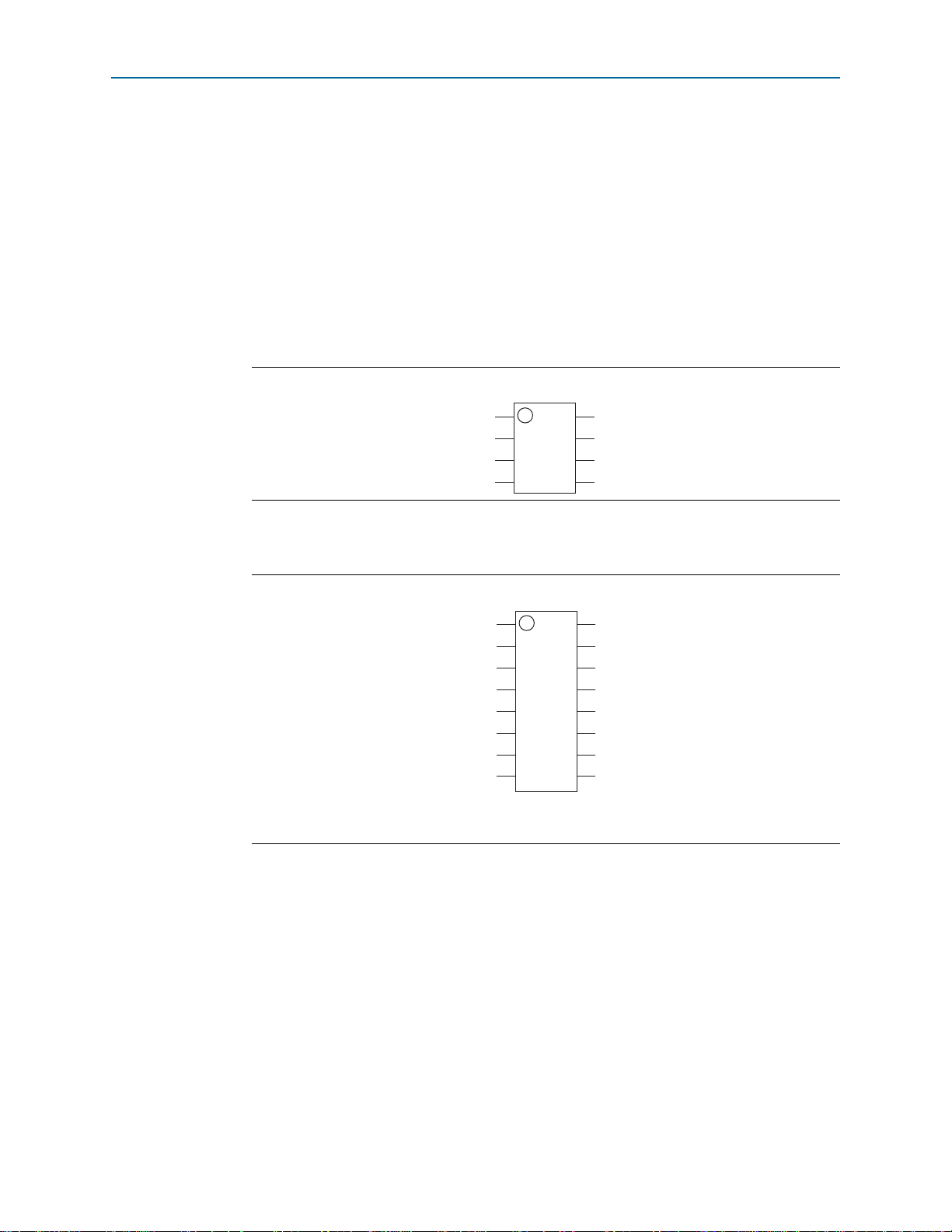
Figure 21 and Figure 22 show the EPCS device in an 8-pin or 16-pin device. The
following lists the control pins on the EPCS device:
■ Serial data output (
■ AS data input (
■ Serial clock (
■ Chip select (
nCS
ASDI
DCLK
)
)
DATA
)
)
Figure 21 shows the 8-pin SOIC package of the EPCS device.
Figur e 21. Altera EPCS De vice 8-Pin SOI C Package Pin-Out Diagram
Figure 22 shows the 16-pin SOIC package of the EPCS device.
Figure 22. Altera EPCS Device 16-Pin SOIC Package Pin-Out Diagram
Note to Figure 22:
(1) You can leave these pins floating or you can connect them to VCC or GND.
Serial Configuration (EPCS) Devices DatasheetJanuary 2012 Altera Corporation
Page 36

Page 36 Pin Information
Pin 1 ID
Pin 1 ID
Ta b l e 2 2 lists the pin description of the EPCS device.
Table 22. EPCS Device Pin Description
Pin
Name
DATA
ASDI
nCS
DCLK
V
CC
GND
Pin Nu mber
in 8-Pin
SOIC
Package
Pin Nu mber
in 16-Pin
SOIC
Package
Pin Type Descrip tion
The
DATA
output signal transfers data serially out of the EPCS device
to the FPGA during the read operation or configuration. During the
28Output
5 15 Input
read operation or configuration, the EPCS devi ce is enabled by pulling
the
nCS
the
The
DCLK
ASDI
signal low. The
signal.
signal is used to transfer data s erially into the EPCS device.
DATA
signal transitions on the falling edge of
This pin are also receiving data that are programmed into the EPCS
device. Data is latched on the rising edge of the
The
nCS
signal toggles at the begi nning and the end of a valid
inst ruction. When this signal goes high, the device is deselected and
the
DATA
17Input
enabled and in an active mode. After power up, the EPCS device
requires a falli ng edge on the
pin is tri-stated. When this signal goes low, the device is
nCS
signal before the EPCS device
begins any operation.
The FPGA provides the
DCLK
signal. This signal provides the timing
for the serial interface. The data presented on the
6 16 Input
to the EPCS device on the rising edge of the
the
DATA
pin changes after the falling edge of the
latched into the FPGA on the next fal ling edge of the
3, 7, 8 1, 2, 9 Power Connect the power pins to a 3.3-V power supply.
4 10 GND Ground pin.
DCLK
signal.
ASDI
pin is latched
DCLK
signal. The da ta on
DCLK
signal and is
DCLK
signal.
Figure 23 shows the layout recommendation for vertical migration from the EPCS1
device to the EPCS128 device.
Figure 23. Layout Recommendation for Vertical Migration from the EPCS1 Device to the EPCS128
Device
Serial Configuration (EPCS) Devices Datasheet January 2012 Altera Corporation
Page 37

Device Package and Ordering Code Page 37
Device Package and Ordering Code
This section describes the package offered in EPCS devices and the ordering codes for
each EPCS device.
Package
The EPCS1, EPCS4, and EPCS16 devices are available in 8-pin SOIC package. The
EPCS64 and EPCS128 devices are available in 16-pin SOIC package.
f For more information, refer to the Package and Thermal Resistance page.
Ordering Code
Ta b l e 2 3 lists the ordering codes for EPCS devices.
Table 23. EPCS Devi ce Ordering Codes
Device Ordering Code
EPCS1
EPCS4
EPCS16 EPCS16SI8N
EPCS64 EPCS64SI16N
EPCS128 EPCS128SI16N
Note to Tab l e 2 3 :
(1) N indicates that the device is lead free.
EPCS1SI8
EPCS1SI8N
EPCS4SI8
EPCS4SI8N
(1)
Document Revision History
Ta b l e 2 4 lists the revision history for this document.
Table 24. Document Revision History (Part 1 of 3)
Date Version Changes
■ Updated “Package” and “Ordering Code” sections.
January 2012 4.0
June 2011 3.4
December 2009 3.3
■ Updated Figure 5, Figure 6, and Figure 22.
■ Updated Ta bl e 16 and Tab le 1 8.
■ Minor text edits.
■ Updated Table 3–19.
■ Updated Figure 3–20.
■ Updated “Features” and “Functional Description” sections.
■ Added “Fast Read Operation” section.
■ Removed Table 4–2 to Table 4–9, Table 4-26, and Ta ble 4–33.
■ Updated Table 3–1.
■ Updated Figure 3–2.
■ Removed “Referenced Documents” section.
Serial Configuration (EPCS) Devices DatasheetJanuary 2012 Altera Corporation
Page 38

Page 38 Document Revision History
Table 24. Document Revision History (Part 2 of 3)
Date Version Changes
■ Updated “Introduction”, “Active Serial FPGA Configuration”, “Operation
Codes”, “Read Status Operat ion”, “Read Devi ce Identification Operation”, and
“Package” sections.
■ Updated Table 4–10, Table 4–25, Table 4–26, and Table 4–32.
October 2008 3.2
May 2008 3.1
■ Updated Figure 4–5, Figure 4–13, and Figure 4–19.
■ Added Figure 4–22.
■ Added Table 4–33.
■ Updated new document format.
■ Updated Table 4–3, Table 4–6, Table 4–7, Table 4–28, and Table 4–29.
■ Deleted Note 5 to Table 4–31.
■ Added “Referenced Documents” section.
■ Updated “Introduction” section.
■ Updated “Functional Description” section.
■ Updated Table 4–1 through Table 4–4 and Table 4–7 through Table 4–9 to with
EPCS128 information.
■ Added Table 4–6 on Arria GX.
■ Added notes to Figure 4–3.
■ Added notes to Figure 4–4.
■ Updated Table 4–10 with EPCS128 information.
■ Added new Table 4–11 on address range for sectors in EPCS128 device.
■ Updated Table 4–16 with information about “Read Device Identification” and
added (Note 5).
August 2007 3.0
■ Added ne w Table 4–21 on block protection bits in EPCS128.
■ Added notes to Figure 4–12.
■ Added new sec tion “Read Device Identif ication Operation” with Table 4–23 and
Figur e 4–13.
■ Updated “Write Bytes Operation”, “Erase Bulk Oper ati on” and “Erase Sector
Operation” sections.
■ Updated Table 4–24 to include EPCS128 information.
■ Updated (Note 1) to Table 4–26.
■ Updated VCC and VI information to include EPCS128 in Table 4–27.
■ Updated VIH information to include EPCS128 in Table 4–29.
■ Updated ICC0 and ICC1 information to include EPCS128 in Table 4–30.
■ Updated Figure 4–21 and Table 4–34 with EPCS128 information.
Serial Configuration (EPCS) Devices Datasheet January 2012 Altera Corporation
Page 39

Document Revision History Page 39
Table 24. Document Revision History (Part 3 of 3)
Date Version Changes
■ Updated “Introduction” section.
■ Updated “Functional Description” section and added handpara note.
■ Added Table 4–4, Table 4–6, and Table 4–7.
April 2007 2.0
January 2007 1.7
October 2006 1.6
August 2005 1.5
August 2005 1.4
■ Updated “Active Serial FPGA Configuration” section and its handpara note.
■ Added notes to Figure 4–2.
■ Updated Table 4–26 and added (Note 1).
■ Updated Figure 4–20.
■ Updated Table 4–34.
■ Removed reference to PLMSEPC-16 in “Progr amming and Configuration Fil e
Support”.
■ Updated DCL K pin information in Table 4–32.
■ Updated Figure 4–19.
■ Updated Table 4–30 and Table 4–32.
■ Updated table 4-4 to include EPCS64 support for Cyclone devices.
■ Updated tables.
■ Minor text updates.
February 2005 1.3 Updated hot socketing AC specifications.
■ Added Serial Configuration Device Memory Access section.
October 2003 1.2
■ Updated timing information in Tables 4–10 and
4–11 section.
■ Updated timing information in Tables 4-16 and 4- 17.
July 2003 1.1 Minor updates.
May 2003 1.0
■ Added document to the Cyclone Device Handbook.
■ Initial release.
Serial Configuration (EPCS) Devices DatasheetJanuary 2012 Altera Corporation
Page 40

Page 40 Document Revision History
Serial Configuration (EPCS) Devices Datasheet January 2012 Altera Corporation
 Loading...