

Page 1
EP1K10 Device Pin-Outs Version 1.4
n
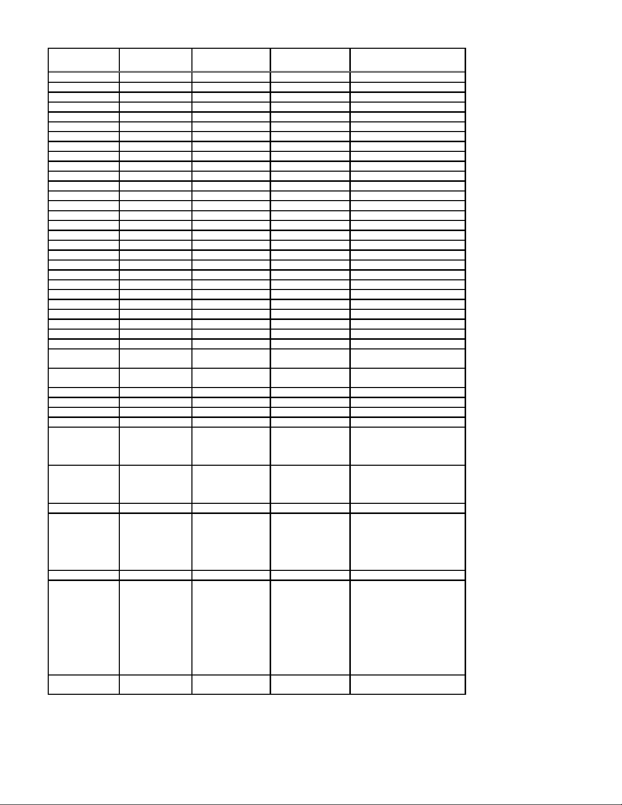
Pin Name (1) 100-Pin TQFP 144-Pin TQFP 208-Pin PQFP 256-Pin FineLine BGA
MSELO (2) 54 77 108 P1
MSEL1 (2) 53 76 107 R1
nSTATUS (2) 25 35 52 T16
nCONFIG (2) 51 74 105 N4
DCLK (2) 75 107 155 B2
CONF_DONE (2) 1 2 2 C15
INIT_DONE (3) 10 14 19 G16
nCE (2) 74 106 154 B1
nCEO (2) 2 3 3 B16
nWS (4) 97 142 206 B14
nRS (4) 96 141 204 C14
nCS (4) 99 144 208 A16
CS (4) 98 143 207 A15
RDYnBUSY (4) 8 11 16 G14
CLKUSR (4) 5 7 10 D15
DATA7 (4) 84 116 166 B5
DATA6 (4) 82 114 164 D4
DATA5 (4) 81 113 162 A4
DATA4 (4) 80 112 161 B4
DATA3 (4) 79 111 159 C3
DATA2 (4) 78 110 158 A2
DATA1 (4) 77 109 157 B3
DATA0 (2), (5) 76 108 156 A1
TDI (2) 73 105 153 C2
TDO (2) 3 4 4 C16
TCK (2) 100 1 1 B15
TMS (2) 24 34 50 P15
TRST (2) - - 51 R16
Dedicated Inputs 38, 40, 89, 91 54, 56, 124, 126 78, 80, 182, 184 B9, E8, M9, R8
Dedicated Clock
39, 90 55, 125 79, 183 A9, L8
Pins
GCLK1 (6) 39 55 79 L8
LOCK (7) 29 42 62 P12
DEV_CLRn (3) 87 122 180 D8
DEV_OE (3) 93 128 186 C9
VCCINT (2.5 V) 12, 35, 52, 60,
72, 92
VCCIO (2.5 or
4, 17, 44, 67, 835, 24, 45, 61,
3.3 V)
16, 50, 75, 85,
103, 127
71, 94, 115, 134
21, 33, 48, 72,
91, 106, 124, 130,
152, 185, 201
5, 22,34, 42, 66,
84, 98, 110, 118,
138, 146, 165,
E11, F12, F5, F7, F9, H10,
H6, H7, J10, J11, J7, K9,
L12, L5, L7, M11, R2
D12, E6, F10, F8, G11, G6,
G8, H11, J6, K11, K6, K8,
L10, M6, N12
178, 194
VCC_CKLK (8) 37 53 77 L9
GNDINT 11,18, 36, 42,
59, 66, 88, 95
15, 25, 40, 52,
58, 66, 84, 93,
123, 129, 139
6, 20, 23, 32, 35,
43, 49, 59, 76,
82, 109, 117, 123,
129, 137, 145,
E12, E5, F11, F6, G10, G7,
G9, H8, H9, J8, J9, K10,
K7, L11, L6, M12, M5, K5,
L1, A14, C7, A3
151, 171, 181, 188
GND_CKLK 41 57 81 T8
No Connect
(N.C.)
- 6, 10, 12, 20,
22, 28, 31, 82,
89, 99, 101, 104
7, 8, 9, 13, 14,
15, 17, 27, 29,
31, 36, 37, 40,
45, 111, 113, 114,
115, 121, 125,
126, 132, 134,
139, 140, 147, 149
C1, D1, D2, D3, D14, D16,
E1, E3, E16, F15, F16, G3,
H1, H3, H4, H14, H16, J1,
K14, K15, K16, L2, L4,
M14, M16, M2, M3, M4, N1,
N14, N15, N2, E14, E15,
F3, F4, F13, F14, L3, L14,
L15, L16, K3, M15, N16,
P2, P11, P14, P16, T1
Total User I/O
66 92 120
Pins (9)
Notes:
1. All pins that are not listed are user I/O pins.
2. This pin is a dedicated pin; it is not available as a user I/O pin.
3. This pin can be used as a user I/O pin if it is not used for its device-wide or configuration function.
4. This pin can be used as a user I/O pin after co
136
Page 2

5. This pin is tri-stated in user mode.
c
6. This pin drives the ClockLock and ClockBoost
7. This pin shows the status of the ClockLock and ClockBoost circuitry. When the ClockLock and ClockBoost circuitry is locked to the incoming clock and generates an
internal clock, LOCK is driven high. LOCK goes low if a periodic clock stops clocking. The LOCK pin is optional; if the LOCK output is not used, this pin is a user I/O pin.
8. This pin is the power or ground for the ClockLock and ClockBoost circuitry of a PLL. To ensure noise resistance, the power and ground supply to the ClockLock and
ClockBoost circuitry should be isolated from the power and ground to the rest of the device.
If the PLL is not used, this power or ground pin should be connected to VCCINT or GNDINT, respectively.
9. The user I/O pin count includes dedicated inputs, dedicated clock inputs, and all I/O pins.
 Loading...