

Page 1

101 Innovation Drive
San Jose, CA 95134
(408) 544-7000
www.altera.com
Cyclone II DSP Development Board
Reference Manual
Document Version: 6.0.1
Document Date: August 2006
Page 2

Copyright © 2006 Altera Corporation. All rights reserved. Altera, The Programmable Solutions Company, the stylized Altera logo, specific device designations, and all other words and logos that are identified as trademarks and/or service marks are, unless noted otherwise, the trademarks and
service marks of Altera Corporation in the U.S. and other countries. All other product or service names are the property of their respective holders. Altera products are protected under numerous U.S. and foreign patents and pending applications, maskwork rights, and copyrights. Altera warrants
performance of its semiconductor products to current specifications in accordance with Altera's standard warranty, but reserves the right to make
changes to any products and services at any time without notice. Altera assumes no responsibility or liability arising out of the application or use of any information, product, or service described herein except as expressly agreed to in writing by Altera
Corporation. Altera customers are advised to obtain the latest version of device specifications before relying on any published information and before placing orders for products or services.
MNL-CII012805-1.1
ii Reference Manual Altera Corporation
Cyclone II DSP Development Board Preliminary August 2006
Page 3

Contents
About This Manual
Revision History ........................................................................................................................................ v
How to Contact Altera .............................................................................................................................. v
Typographic Conventions ...................................................................................................................... vi
Chapter 1. Introduction
Introduction ............................................................................................................................................ 1–1
Features Overview ................................................................................................................................. 1–1
Components ...................................................................................................................................... 1–1
Chapter 2. Cyclone II DSP Development Board Components
Introduction ............................................................................................................................................ 2–1
Components & Interfaces ..................................................................................................................... 2–1
Featured Device ..................................................................................................................................... 2–9
User Interfaces ........................................................................................................................................ 2–9
User-Defined LEDs (D2 Through D9) ......................................................................................... 2–10
User Defined DIP Switch (S1) ....................................................................................................... 2–11
User-Defined Pushbuttons (SW2 Through SW5) ...................................................................... 2–12
Seven-Segment Display (U32,U33) .............................................................................................. 2–13
Audio CODEC Converter (U11) .................................................................................................. 2–14
Audio Jacks (J10, J14, J16) .............................................................................................................. 2–14
VGA Output Connector (J21) ....................................................................................................... 2–15
VGA Triple Video D/A Output Converter (U21) ..................................................................... 2–15
D/A Converter SMA Connector (J31 & J43) .............................................................................. 2–17
D/A Converter Clock Buffer (U27 & 30) .................................................................................... 2–17
D/A Converter (U25 & U30) ........................................................................................................ 2–17
A/D Converter Data Format Select Jumper (J30 & J38) ........................................................... 2–21
A/D Converter SMA Connector (J32 & J44) .............................................................................. 2–21
A/D Converter Clock Buffer (U29 & U28) ................................................................................. 2–22
A/D Converter (U26 & U31) ........................................................................................................ 2–22
Memory Components ......................................................................................................................... 2–26
DDR2 SDRAM DIMM (J8) ............................................................................................................2–26
DIMM_SYNC_CLK SMA Connector (J11) ................................................................................. 2–36
SSRAM Sleep & Run Modes (J24) ................................................................................................ 2–37
EPCS Select (J29) ............................................................................................................................. 2–37
EPCS64 Flash Memory Devices (U17, U36) ................................................................................ 2–38
Synchronous SRAM Device (U22) ............................................................................................... 2–39
Memory Mapping to the TMS320C6416 Digital Signal Processor .......................................... 2–42
Expansion Connectors ........................................................................................................................ 2–43
Expansion Prototype Connector (J15, J22 & J23) ....................................................................... 2–43
Expansion TI-EVM Connectors (U34, U40) ................................................................................ 2–47
Altera Corporation Reference Manual iii
August 2006 Cyclone II DSP Development Board
Page 4

Contents
General Connectors ............................................................................................................................. 2–50
JTAG Connector (J9) ...................................................................................................................... 2–50
Active Serial Interface (ASI) Connector (J13) ............................................................................. 2–52
Mictor Connector (J12) ................................................................................................................... 2–53
Status LEDs & Reset/Power Switches ..............................................................................................2–57
Power (D1) & Status (D10) LEDs ................................................................................................. 2–57
Power Switch (SW1) ....................................................................................................................... 2–57
User Defined Reset (SW6) Push-Button ...................................................................................... 2–57
System Reset (SW7) Push-Button ................................................................................................. 2–58
Clock Circuitry ..................................................................................................................................... 2–59
Setting the Clocks ........................................................................................................................... 2–60
CLK SMA Connector (J17) ............................................................................................................ 2–61
On-Board/Custom Clock Oscillators Select Jumper (J18) ........................................................ 2–61
Clock Select Jumper (J19) .............................................................................................................. 2–62
Socket for a Custom Clock Oscillator (J20) ................................................................................. 2–62
D/A Converter CLK SMA Connector (J26) ................................................................................ 2–62
A/D Converter CLK SMA Connector (J27) ................................................................................ 2–62
D/A Converter CLK Select Jumper (J35 & J34) ......................................................................... 2–62
A/D Converter CLK Select Jumper (J37 & J36) ......................................................................... 2–62
D/A Converter Power Select Jumper (J33) ................................................................................ 2–63
Clock Buffer (U16) .......................................................................................................................... 2–64
On-Board Clock Oscillator (U20) .................................................................................................2–64
Power Supply ....................................................................................................................................... 2–65
DC Power Input Jack (J1) .............................................................................................................. 2–65
Voltage Limiter Switches (U13-U15, U18 & U19) ...................................................................... 2–66
On-Board Power Regulators (U2, U7, U8, U9, U10, U23 & U24) ............................................ 2–66
Bench Power Supplies Using Banana Jacks ................................................................................ 2–67
Power Plane Connectors (J2-J6, J39 Through J42) ...................................................................... 2–69
Appendix A. DDR2 SDRAM DIMM Connector Pin Out Table
Introduction ........................................................................................................................................... A–1
Appendix B. SSRAM Pin-Out Table
Introduction ........................................................................................................................................... B–1
Appendix C. Cyclone II EP2C70 Device Pin-Out Table
Introduction ........................................................................................................................................... C–1
Appendix D. Restoring the Factory Design
Introduction ........................................................................................................................................... D–1
Factory-Programmed Factory Design .......................................................................................... D–1
User Designs .................................................................................................................................... D–1
Reprogramming the Factory Design to the EPSC64 Device (U17) .......................................... D–1
iv Reference Manual Altera Corporation
Cyclone II DSP Development Board August 2006
Page 5
About This Manual
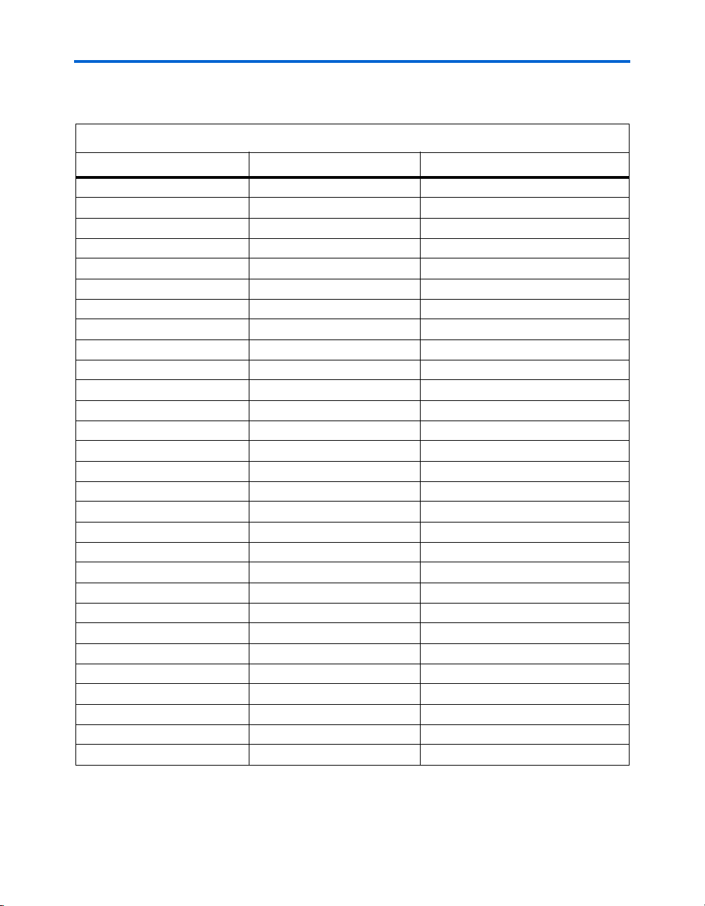
Revision History
Chapter Date Version Changes Made
All May 2005 1.0.0 First publication
All August 2006 6.0.1 Updated for Quartus II Release 6.0 Service Pack 1
How to Contact Altera
Information Type USA & Canada All Other Locations
Technical support www.altera.com/mysupport/ www.altera.com/mysupport/
Product literature www.altera.com www.altera.com
Altera literature services lit_req@altera.com lit_req@altera.com
Non-technical customer
service
FTP site ftp.altera.com ftp.altera.com
The table below displays the revision history for the chapters in this
manual.
For technical support or other information about Altera® products, go to
the Altera world-wide web site at www.altera.com. You can also contact
Altera through your local sales representative or any of the sources listed
below.
800-800-EPLD (3753)
7:00 a.m. to 5:00 p.m. Pacific Time
800-767-3753 + 1 408-544-7000
+1 408-544-8767
7:00 a.m. to 5:00 p.m. (GMT -8:00)
Pacific Time
7:00 a.m. to 5:00 p.m. (GMT -8:00)
Pacific Time
Altera Corporation Reference Manual v
August 2006 Cyclone II DSP Development Board
Page 6
Typographic Conventions
Typographic
This document uses the typographic conventions shown below.
Conventions
Visual Cue Meaning
Bold Type with Initial
Capital Letters
bold type External timing parameters, directory names, project names, disk drive names,
Italic Type with Initial
Capital Letters
Italic type Internal timing parameters and variables are shown in italic type.
Initial Capital Letters Keyboard keys and menu names are shown with initial capital letters.
“Subheading Title” References to sections within a document and titles of on-line help topics are shown
Courier type
Command names, dialog box titles, checkbox options, and dialog box options are
shown in bold, initial capital letters.
Example: Save As dialog box.
filenames, filename extensions, and software utility names are shown in bold type.
Examples: f
Document titles are shown in italic type with initial capital letters.
Example: AN 75: High-Speed Board Design.
Examples: t
Variable names are enclosed in angle brackets (< >) and shown in italic type. Example:
<file name>, <project name>.pof file.
Examples: Delete key, the Options menu.
in quotation marks.
Example: “Typographic Conventions.”
Signal and port names are shown in lowercase Courier type.
Examples:
Active-low signals are denoted by suffix
, \qdesigns directory, d: drive, chiptrip.gdf file.
MAX
, n + 1.
PIA
data1, tdi, input.
n, for example, resetn.
Anything that must be typed exactly as it appears is shown in Courier type (for
example:
Also, sections of an actual file, such as a Report File, references to parts of files (for
example, the AHDL keyword
example,
1., 2., 3., and
a., b., c., and so on
● • Bullets are used in a list of items when the sequence of the items is not important.
■
v The checkmark indicates a procedure that consists of one step only.
1 The hand points to information that requires special attention.
c
w
r The angled arrow indicates you should press the Enter key.
f The feet direct you to more information on a particular topic.
vi Reference Manual Altera Corporation
Cyclone II DSP Development Board August 2006
Numbered steps are used in a list of items when the sequence of the items is
important, such as the steps listed in a procedure.
The caution indicates required information that needs special consideration and
understanding and should be read prior to starting or continuing with the procedure or
process.
The warning indicates information that should be read prior to starting or continuing
the procedure or processes
c:\qdesigns\tutorial\chiptrip.gdf.
SUBDESIGN), as well as logic function names (for
TRI) are shown in Courier.
Page 7

Chapter 1. Introduction
Introduction
Features Overview
This document describes the hardware features of the Cyclone™ II DSP
development board, including detailed pin-out information, to enable
designers to create custom FPGA designs that interface with all
components on the board.
f For information on setting up and powering up the Cyclone II DSP
development board and installing the included software, refer to the
DSP Development Kit, Cyclone II Edition Getting Started User Guide.
The Cyclone II DSP development board is included in the
DSP Development Kit, Cyclone II Edition (ordering code DK-DSP-2C70N).
The Cyclone II DSP development board provides a low-cost hardware
platform for developing high performance DSP designs based on Altera
Cyclone II FPGA devices. The DSP Development Kit, Cyclone II Edition
features the EP2C70F672 FPGA.
Components
■ Analog I/O
● Two 14-bit analog-to-digital (A/D) converter channels with
125 MSPS and 70 dB signal-to-noise ratio capabilities
● Two 14-bit digital-to-analog (D/A) converter channels with
165 MSPS and 70 dB signal-to-noise ratio capabilities
● One 24-bit RGB VGA adapter with a DB-15 connector
● One Audio CODEC with input, output, and amplified output
■ Memory Subsystem
● 256 Mbyte DDR2 SDRAM DIMM
● 1 Mbyte synchronous SRAM (SSRAM)
■ Two EPCS64 64 Mbit serial configuration devices
■ Debugging Interface—Mictor connector for hardware and software
debugging
■ Expansion Interfaces
● 3.3-V/5-V tolerant Altera expansion/prototype headers
● One Texas Instruments Evaluation Module (TI-EVM) expansion
connector to connect to the Spectrum Digital DSP Starter Kit
(DSK) for the TMS320C6416, Revision E
■ Dual seven-segment LED displays
■ Eight user-defined LEDs
®
Altera Corporation Reference Manual 1–1
August 2006 Preliminary
Page 8
Features Overview
■ One user programmable dual in-line package (DIP) switch
(8 positions)
■ Four user-defined push-buttons
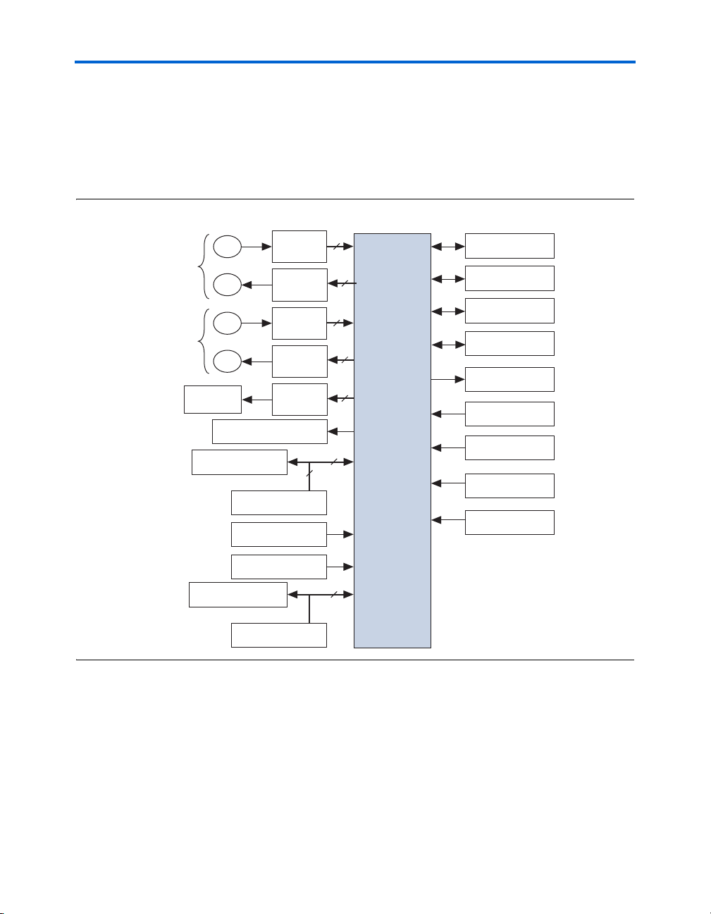
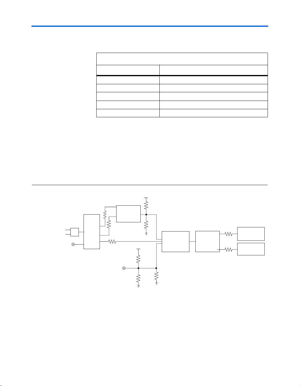
Figure 1–1 shows a functional diagram of the Cyclone II DSP
development board.
Figure 1–1. Cyclone II DSP Development Board Functional Diagram
Channel A
Channel B
Connector
Altera Daughter Card
SMA
SMA
SMA
SMA
DB-15
Seven-Segment Display
TI-EVM Connector
256K X 36 SSRAM
100-MHz
On-Board Oscillator
Custom Oscillator
Mictor Connector
A/D
Converter
D/A
Converter
A/D
Converter
D/A
Converter
VGA
DDR2
14
14
14
Cyclone II
FPGA
14
24
75
32
41
SDRAM DIMM
JTAG Connector
ASI Connector
Audio CODEC
User-Defined
LEDs
User-Defined
Pushbuttons
User-Defined
Dipswitches
Flash Memory
Safe Mode
Flash Memory
User Mode
1–2 Reference Manual Altera Corporation
Cyclone II DSP Development Board August 2006
Page 9

Chapter 2. Cyclone II DSP
Development
Board Components
Introduction
Components & Interfaces
f Software and hardware installation and setup are described in the DSP
This chapter describes the Cyclone II DSP development board
components.
This section introduces the major components on the Cyclone II DSP
development board by first listing them in Table 2–1 on page 2–4. A
detailed description of each component comprises the remainder of this
chapter.
1 A schematic, a physical layout database, and manufacturing
files for the Cyclone II DSP development board are included in
the DSP Development Kit, Cyclone II Edition at the following
directory:
<install-path>\CycloneII_DSP_Kit-v6.0.1\BoardDesignFiles
Development Kit, Cyclone II Edition Getting Started User Guide.
Altera Corporation Reference Manual 2–1
August 2006 Preliminary
Page 10
Components & Interfaces
)
Figure 2–1 shows the front view of the Cyclone II DSP development
board.
Figure 2–1. Cyclone II DSP Development Board, Front View
Power Switch (SW1)
Power LED (D1)
Single Slot DDR2
SDRAM DIMM Connector (J8)
GND Connector (J2)
DC Power Jack (J1)
On-Board Power
Regulator (U9)
Line In Audio Jack (J10)
DIMM SYNC CLK
SMA Connector (J11)
Audio CODEC Converter (U11)
Line Out Audio Jack (J14)
CLK SMA Connector (J17)
Headphone Jack (J16)
Clock Oscillator Select Jumper (J18)
D/A Converter Clock SMA Connector (J26)
Clock Buffer (U16)
Clock Select Jumper (J19)
VGA Output Connector (J21)
DAC Power Supply Jumper (J25)
VGA Triple Video D/A
Output Converter (U21)
SSRAM (U22)
SMA to D/A Output
Converter Connector (J31)
D/A Output Converter (U25)
DAC PWR Jumper (J33)
DAC Clock Select Jumper (J35)
VCCA DAC (J39)
On-Board Power Regulator (U23)
Custom Clock Oscillator Socket (J20)
On-Board Clock Oscillator (U20)
User-Defined Push-Button Switches
(SW2, SW3, SW4, SW5)
User-Defined LEDs (D2, D3, D4, D5, D6, D7, D8, D9)
(Overlay)
SSRAM SLEEP Mode or RUN Mode Jumper (J24)
Power Plane Connector (J3)
DAC Clock Buffer (U27)
Cyclone II FPGA (U12)
User-Defined DIP Switch (S1)
On-Board Power
Regulator (U2)
Unused (J36)
User-Defined Reset Push-Button (SW6)
Power Plane Connectors (J4, J5)
System Reset Push-Button (SW7)
ADC Clock Select Jumper (J37)
ADC Differential LVPECL Buffer (U29)GND DAC (J40)
Dual Seven-Segment Display (U32, U33)Unused (J34)
On-Board Power Regulator (U7)
Power Plane Connector (J6)
Bench Power Supply
Select Jumper (J7)
On-Board Power
Regulators (U8, U10)
JTAG Connector (J9)
Mictor Connector (J12)
ASI Connector (J13)
Expansion Prototype
Connector (J15)
Voltage Limiter Switches
(U13, U14, U15, U18, U19)
SAFE EPCS (U17)
(Flash Memory)
Expansion Prototype
Connectors (J22, J23)
A/D Converter Clock
SMA Connector (J27)
EPCS Select Jumper (J29)
ADC PWR Jumper (J28)
DFS Jumper (J30)
SMA to A/D Input
Converter Connector (J32)
A/D Input Converter (U26)
On-Board Power Regulator (U24
VCCA ADC (J42)
GND ADC (J41)
Status LED (D10)
(CONF DONE)
2–2 Reference Manual Altera Corporation
Cyclone II DSP Development Board August 2006
Page 11
Cyclone II DSP Development Board Components
Figure 2–2 shows the back view of the Cyclone II DSP development
board.
Figure 2–2. Cyclone II DSP Development Board, Back View
USER EPCS (U36)
(Flash Memory)
(1) For Spectrum Digital DSP Starter Kit
TI-EVM PERIPHERAL Expansion Connector U34 (1)
TI-EVM MEMORY Expansion Connector U40 (1)
Altera Corporation Reference Manual 2–3
August 2006 Cyclone II DSP Development Board
Page 12
Components & Interfaces
Table 2–1 describes the major components on the Cyclone II DSP
development board and the related interfaces.
Table 2–1. Cyclone II DSP Development Board Components & Interfaces (Part 1 of 5)
Board Reference Name Description Page
Featured Device 2–9
U12 Cyclone™ II FPGA EP2C70F672-C6 2–9
User Interfaces 2–9
D2, D3, D4, D5, D6, D7,
D8, D9
S1 User-defined DIP
SW2, SW3, SW4, SW5 User-defined
U32, U33 Dual seven-segment
J10 Line-in audio jack Audio input connector for line-in (2.5 mm). 2–14
J14 Line-out audio jack Audio output connector for line-out (2.5 mm).
J16 Headphone jack Amplified audio output connector for
U11 Audio CODEC
J21 VGA output
U21 VGA triple video D/A
J31 (Channel A)
J43 (Channel B)
J26 (Channel A & B) D/A converter CLK
U25 (Channel A)
U30 (Channel B)
J32 (Channel A)
J44 (Channel B)
J27 (Channel A & B) A/D converter CLK
U26 (Channel A)
U31 (Channel B)
User-defined LEDs Eight user-defined LEDs. 2–10
One User-defined octal DIP switch. 2–11
switch
User-defined momentary-contact push-button
push-button switches
display
converter
connector
output converter
D/A converter output
SMA connector
SMA connector
D/A converter Texas Instruments DAC904E 14-bit
A/D converter input
SMA connector
SMA connector
A/D converter Texas Instruments ADS5520 12-bit 125 MSPS
switches.
Dual seven-segment display. 2–13
headphones (2.5 mm).
Texas Instruments TLV320AIC23 96 kHz stereo
audio CODEC.
VGA output connector (DB-15). 2–15
Fairchild FMS3818 triple video D/A output
converter.
SMA connector which is driven by the output of
the Channel A D/A converter (U25).
SMA connector for an external D/A converter
clock input to U25.
digital-to-analog (D/A) converter.
SMA connector which drives the Channel A A/D
converter (U26).
SMA connector for an external A/D converter
clock input to U26.
analog-to-digital (A/D) converter.
2–12
2–14
2–15
2–17
2–62
2–17
2–21
2–62
2–22
2–4 Reference Manual Altera Corporation
Cyclone II DSP Development Board August 2006
Page 13
Cyclone II DSP Development Board Components
Table 2–1. Cyclone II DSP Development Board Components & Interfaces (Part 2 of 5)
Board Reference Name Description Page
Memory Components 2–26
J8 Single slot connector
for DDR2 SDRAM
DIMM
U17, U36 EPCS64 flash
memory
U22 SSRAM Cypress Semiconductor CY7C1360B-166AC,
Micron Technology MT8HTF3264AY-40E,
256 Mbyte, 32 Mbyte x 64, 167 MHz, 1.8 V,
240-pin, non-ECC, unbuffered DDR2 SDRAM
DIMM.
Two EPCS64 64 Mbit flash memory, serial
configuration devices used to store the safe
(factory) design (U17) and a user design (U36).
The EPCS64 device configures the EP2C70
FPGA by downloading the factory design or the
user design to the EP2C70 FPGA each time the
Cyclone II DSP development board powers up
or on board reset. J29 determines which design
is used.
9 Mbit, 256 Kbit x 36-bit/512 Kbit x 18 pipelined
synchronous SRAM (SSRAM).
The TMS320C6416 processor memory maps to
the Cyclone II DSP development board’s
SSRAM and the EP2C70 FPGA through the
EMIF connector (U34 and U40).
Expansion Connectors
J15, J22, J23 Expansion Prototype
Connector
U34, U40 Expansion TI-EVM
connectors
Three connectors collectively called the
Expansion Prototype Connector. They are used
to connect to Altera daughter cards or for
debugging and prototyping purposes.
Connects to the EMIF connector on the
TMS320C6416 DSK development board.
U34 and U40 are located on the back of the
Cyclone II DSP development board.
General Connectors
J9 JTAG connector The Joint Test Action Group (JTAG) connector
J13 ASI connector The active serial interface (ASI) connector is
J12 Mictor connector The Mictor connector used for hardware and
J17 CLK SMA connector SMA connector for an external clock input to
is used to directly configure the EP2C70 FPGA.
used to program the EPCS64.
software debugging. It can be used with
external scopes or external logic analyzers.
U16 to generate FPGA clocks.
2–26
2–38
2–39
2–42
2–43
2–43
2–47
2–50
2–50
2–52
2–53
2–61
Altera Corporation Reference Manual 2–5
August 2006 Cyclone II DSP Development Board
Page 14
Components & Interfaces
Table 2–1. Cyclone II DSP Development Board Components & Interfaces (Part 3 of 5)
Board Reference Name Description Page
J11 DIMM_SYNC_CLK
SMA connector
The SMA connector (
test point SMA for eye diagrams of DDR2
signals using AC-coupled SMA connections to
an oscilloscope.
DIMM_SYNC_CLK) is a
Jumpers
J18 On-board or custom
clock oscillator select
jumper
J19 Clock select jumper Jumper that determines which input to U16 (the
J24 SSRAM SLEEP
mode or RUN mode
jumper
J7 5 V enable/disable
jumper for U10
J25 D/A converter power
J28 A/D converter power
J33 D/A converter voltage
J29 EPCS select jumper Jumper that selects the configuration mode
J30 (Channel A)
J38 (Channel B)
J35 (Channel A)
J34 (Channel B)
J37 (Channel A)
J36 (Channel B)
supply jumper
supply jumper
select jumper
Data Format Select
(DFS) jumper
D/A converter clock
select jumper
A/D converter clock
select jumper
Jumper that determines if the on-board clock
100 MHz oscillator (U20) or a custom clock
oscillator (J20) becomes the input clock
oscillator to the clock buffer (U16).
selected clock oscillator or the SMA clock) will
be used to determine the clock outputs of U16.
Jumper that selects SLEEP mode or RUN mode
on the SSRAM.
J7 disables the on-board 5-volt voltage
regulator (U10) output to eliminate all regulatorbased noise.
Jumper that selects whether the D/A converter
is powered from the DC input jack or the bench
power supply connector (J39 and J40).
Jumper that selects whether the A/D converter
is powered from the DC input jack or the bench
power supply connector (J42 and J41).
Jumper that determines whether the D/A
converter is powered at 3.3 volts or 5.0 volts.
(SAFE EPCS or USER EPCS)
Data Format Select (DFS) jumper selects the
data output format from the Texas Instruments
ADS5520 A/D converter (U26 and U31). There
are four data output formats.
D/A Converter Channel A clock select jumper. It
determines the D/A converter clock from three
input clock signals, the OSC clock, the FPGA
D/A converter clock, or the SMA clock (J26).
A/D converter Channel A clock select jumper. It
determines the A/D converter clock from three
input clock signals, the OSC clock, the FPGA
A/D converter clock, or the SMA clock (J27).
2–36
2–61
2–62
2–37
2–69
2–70
2–70
2–63
2–37
2–21
2–62
2–62
2–6 Reference Manual Altera Corporation
Cyclone II DSP Development Board August 2006
Page 15

Cyclone II DSP Development Board Components
Table 2–1. Cyclone II DSP Development Board Components & Interfaces (Part 4 of 5)
Board Reference Name Description Page
Status LEDs & Reset/Power Switches 2–57
D1 Power LED Indicates when power is present. 2–57
D10 Status LED Indicates successful configuration of the
Cyclone II DSP development board
(
CONFIG_DONEn is asserted).
SW1 Power switch Power switch that is used to apply power to the
on-board power regulators.
SW6 User-defined reset
push-button
SW7 System reset
push-button
Clocks 2–59
J20 Socket for connecting
custom clock
oscillator
U16 Clock buffer U16 is the clock buffer for the five clocks on the
U20 On-board clock
oscillator
U27 D/A converter clock
buffer
U29 A/D converter
differential LVPECL
buffer
U28 A/D converter
differential LVPECL
buffer
USER RESET is user-defined
momentary-contact push-button used to reset
and initialize a user design on the Cyclone II
DSP development board.
SYS RESET is a momentary-contact pushbutton used to reset the hardware and configure
the Cyclone II DSP development board with the
design stored in the EPCS64 selected by J29.
Socket on top of U20 where a half-can clock
oscillator can be installed. It is referred to as the
custom clock oscillator. It can be an input to
U16.
Cyclone II DSP development board.
The on-board clock oscillator is the ECS, Inc.
ECS-3953M-1000-BN-TR 100 MHz surface
mount oscillator. It can be an input to U16.
U27 uses the DAC_A clock selected by J35 and
inputs it to U25, and uses the DAC_B clock
selected by J34 and inputs it to U30.
U29 uses the ADC_A clock selected by J37 and
inputs it to U26.
U28 uses the ADC_B clock selected by J36 and
inputs it to U31.
2–57
2–57
2–58
2–62
2–64
2–64
2–17
2–22
2–22
Altera Corporation Reference Manual 2–7
August 2006 Cyclone II DSP Development Board
Page 16
Components & Interfaces
Table 2–1. Cyclone II DSP Development Board Components & Interfaces (Part 5 of 5)
Board Reference Name Description Page
Powe r S up ply 2–65
J1 DC power jack 9-20 V DC power source.
U13, U14, U15, U18, U19 Voltage limiter
switches
U2, U7, U8, U9, U10,
U23, U24
J2, J3, J4, J5, J6, J39,
J40, J41, J42
On-board power
regulators
Power plane
connectors
For information on powering up and testing the
Cyclone II DSP development board, see
“Cyclone II DSP Development Board Power-Up”
on page 2–65. For isolating and testing the
power planes, see “Bench Power Supplies
Using Banana Jacks” on page 2–67.
10-bit, 2-port bus switch. 2–66
Seven voltage regulators on the Cyclone II DSP
development board.
Connectors for bench power supplies. 2–69
2–65
2–66
2–8 Reference Manual Altera Corporation
Cyclone II DSP Development Board August 2006
Page 17
Cyclone II DSP Development Board Components
Featured Device
f For details about configuring the EP2C70 FPGA, see the Getting Started
The DSP Development Kit, Cyclone II Edition features the EP2C70F672
®
FPGA (U12) in a 672-pin FineLine BGA
package. Table 2–2 lists the
“Power Switch (SW1)” on page 2–57features of this device.
Table 2–2. Cyclone II EP2C70F672 Features
Feature Value
Embedded 18x18 multipliers 150
Logic Elements (LEs) 68,416
M4K RAM blocks (4 Kbits + 512 parity bits) 250
Maximum differential channels 262
PLLs 4 PLLs
Total RAM bits 1,152,000
User I/O pins 422
You can configure the FPGA in one of two ways:
■ Use Quartus II to program a SRAM Object file (SOF) file directly into
the FPGA via the JTAG connector.
chapter in the DSP Development Kit, Cyclone II Edition Getting Started User
Guide.
■ Use Quartus II to load a design into the EPCS64 device via the ASI
connector and then cycle power to load the design from the EPCS64
device into the FPGA.
There are two EPCS64 devices, J29 determines which EPCS64 device
loads the FPGA. Refer to “EPCS64 Flash Memory Devices (U17,
U36)” on page 2–38 for more information.
User Interfaces
This section describes the user interfaces, which consist of LEDs,
switches, push-buttons, seven-segment display, line in, line out, audio
and headphone jacks, VGA, D/A converter, and A/D converter.
Altera Corporation Reference Manual 2–9
August 2006 Cyclone II DSP Development Board
Page 18
User Interfaces
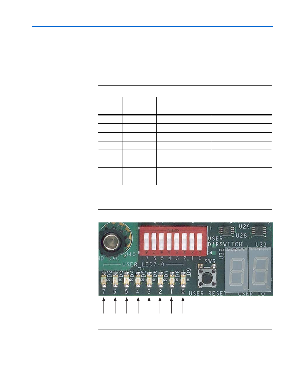
User-Defined LEDs (D2 Through D9)
The Cyclone II DSP development board provides eight user-defined
LEDs. D2 through D9 are connected to general purpose I/O pins on the
EP2C70 FPGA as listed in Table 2–3. When the EP2C70 FPGA drives logic
0, the corresponding LED turns on.
Table 2–3. User-Defined LED Pin-Outs
LED
Number
7D2
6D3
5D4
4D5
3D6
2D7
1D8
0D9
Board
Reference
Schematic Signal
Name
USER_LED7 AA7
USER_LED6 AA6
USER_LED5 AB4
USER_LED4 AC3
USER_LED3 E22
USER_LED2 F20
USER_LED1 B3
USER_LED0 E5
Figure 2–3 shows the user-defined LEDs.
Figure 2–3. User-Defined LED0 Through LED7
Cyclone II (U12) Pin
Number
7 D26 D35 D44 D53 D62 D71 D80
2–10 Reference Manual Altera Corporation
Cyclone II DSP Development Board August 2006
D9
Page 19
Cyclone II DSP Development Board Components
User Defined DIP Switch (S1)
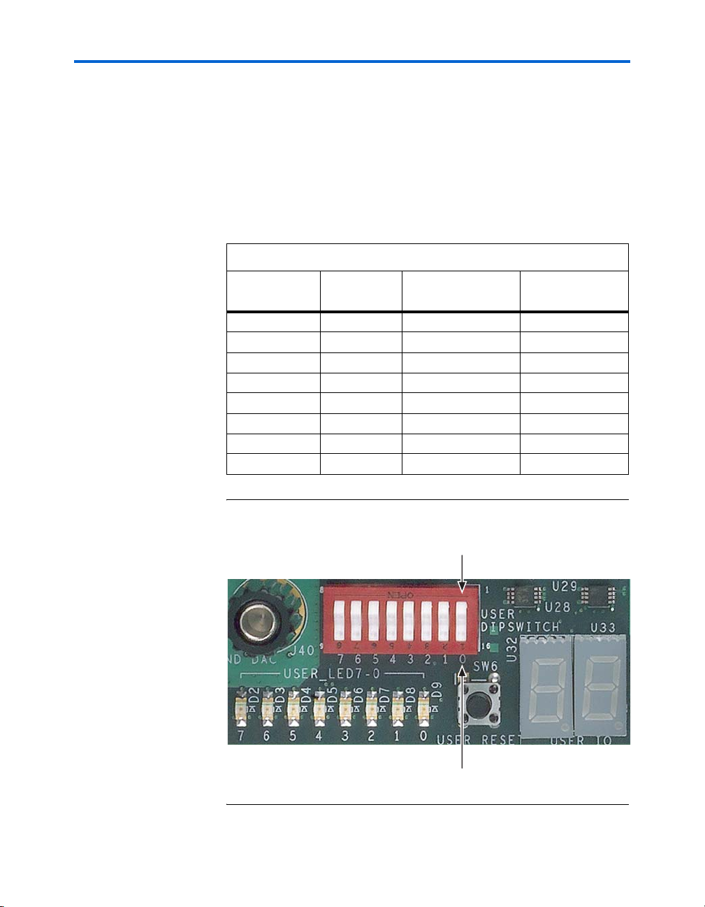
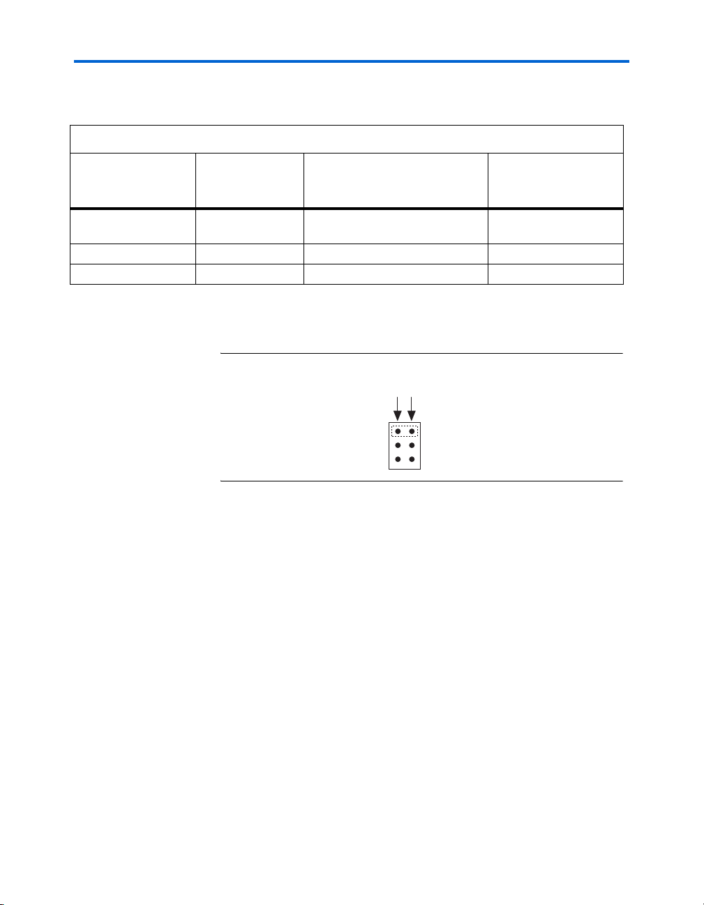
S1 is a user-defined octal DIP switch available for general-purpose use. It
must be defined by the user before it can be used. In the open position,
the selected signal is driven to logic 1. In the closed position, the selected
signal is driven to logic 0. Table 2–4 lists the pin-outs of the user DIP
switch. Figure 2–4 shows the switch labels on the switch, the labels on the
printed circuit board (PCB), and shows the open and closed switch
positions.
Table 2–4. User-Defined Dipswitch Pin-Outs
DIP Switch
Label
10
21
32
43
54
65
76
87
Board
Reference
Schematic Signal
USER_DIPSW0 AC13
USER_DIPSW1 A19
USER_DIPSW2 C21
USER_DIPSW3 C23
USER_DIPSW4 AF4
USER_DIPSW5 AC20
USER_DIPSW6 AE18
USER_DIPSW7 AE19
Figure 2–4. User-Defined Dipswitch (S1)
Name
Open Position
Logic 1
Cyclone II (U12)
Pin Number
Closed Position
Logic 0
Altera Corporation Reference Manual 2–11
August 2006 Cyclone II DSP Development Board
Page 20
User Interfaces
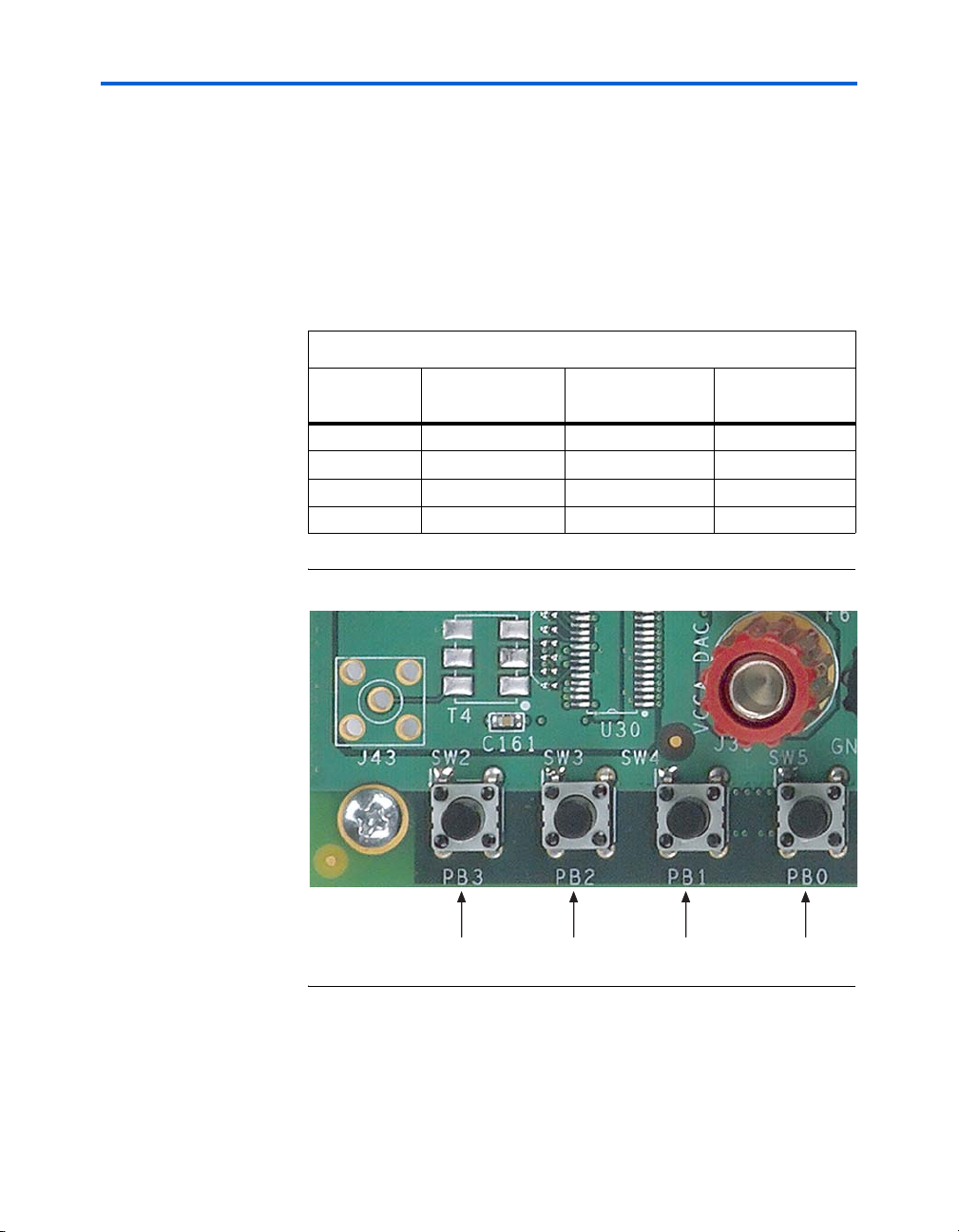
User-Defined Pushbuttons (SW2 Through SW5)
SW2-SW5 are user-defined momentary-contact push-button switches
used to provide stimulus to a user design on the Cyclone II DSP
development board. Each push-button is connected to the EP2C70
general-purpose I/O pin as listed in Table 2–5. When the switch is
pressed and held down, the device pin is set to logic 0, when the switch
is released, the device pin is set to logic 1. Figure 2–5 shows the
push-buttons.
Table 2–5. User-Defined Push-Button Pin-Outs
Push-Button
Name
PB3 SW2
PB2 SW3
PB1 SW4
PB0 SW5
Board Reference
Figure 2–5. User-Defined Pushbuttons
Schematic Signal
Name
Cyclone II (U12)
Pin Number
USER_PB3 AE14
USER_PB2 AE22
USER_PB1 AE16
USER_PB0 AC18
SW2
PB3
2–12 Reference Manual Altera Corporation
Cyclone II DSP Development Board August 2006
SW3
PB2
SW4
PB1
SW5
PB0
Page 21
Cyclone II DSP Development Board Components
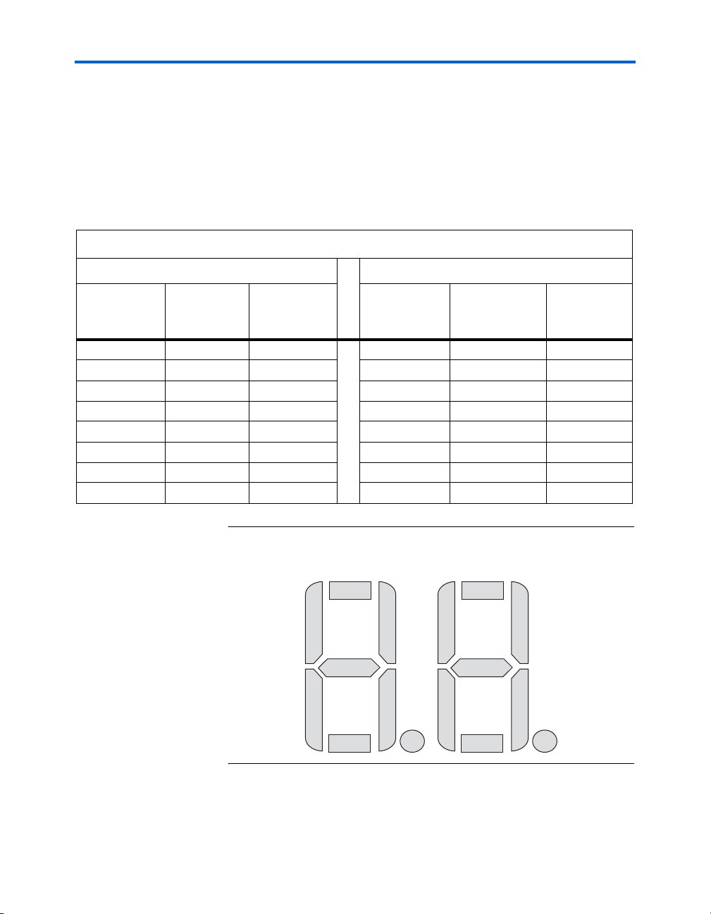
Seven-Segment Display (U32,U33)
U32 and U33 are dual user defined, seven-segment displays on the
Cyclone II DSP development board. Each segment is individually
controlled by a general purpose I/O pin. When the EP2C70 FPGA pin
drives logic 0, the corresponding segment turns on. Table 2–6 lists the
seven-segment display pin-outs. Figure Figure 2–6 shows the name of
each segment.
Table 2–6. Seven-Segment Display Pin-Outs
U32 U33
Segment
Display Name
A
B
C
D
E
F
G
DP
Schematic
Signal Name
DIG_MSB_A Y21
DIG_MSB_B T7
DIG_MSB_C AB23
DIG_MSB_D Y5
DIG_MSB_E E1
DIG_MSB_F U1
DIG_MSB_G W21
DIG_MSB_DP V3
Cyclone II
(U12) Pin
Name
Figure 2–6. Segment Names for the Dual Seven-Segment Displays
Segment
Display Name
A
B
C
D
E
F
G
DP
U32
A
F
B
G
Schematic
Signal Name
DIG_LSB_A K2
DIG_LSB_B U25
DIG_LSB_C AA3
DIG_LSB_D V1
DIG_LSB_E V7
DIG_LSB_F U23
DIG_LSB_G AC2
DIG_LSB_DP P7
U33
A
F
B
G
Cyclone II
(U12) Pin
Name
CE
D
Altera Corporation Reference Manual 2–13
August 2006 Cyclone II DSP Development Board
DP
CE
D
DP
Page 22
User Interfaces
Audio CODEC Converter (U11)
The Cyclone II DSP development board contains three stereo jack
connectors, which provide one stereo output, one stereo input, and one
amplified stereo headphone output. The stereo jacks are driven by a
stereo audio CODEC running at 8-96 kHz. Table 2–7 lists the audio
CODEC references.
Table 2–7. Audio CODEC Reference
Item Description
Board reference U11
Part number TLV320AIC23
Device description Stereo Audio CODEC, 8-96 kHz
Manufacturer Texas Instruments
Manufacturer web site www.ti.com
Table 2–8 lists the TI TLV320AIC23 audio CODEC pin-outs.
Table 2–8. TI TLV320AIC23 Audio CODEC Pin-Outs
Schematic Signal Name
AUDIO_BCLK 3 F3
AUDIO_CLK 25 AB3
AUDIO_CSN 21 AC25
AUDIO_DIN 4 J21
AUDIO_DOUT 6 B13
AUDIO_LRCIN 5 W4
AUDIO_LRCOUT 7 AB2
AUDIO_MODE 22 AA2
AUDIO_SCLK 24 R4
AUDIO_SDIN 23 AD2
Audio CODEC (U11) Pin
Number
Cyclone II (U12) Pin
Number
Audio Jacks (J10, J14, J16)
The Cyclone II DSP development board contains the following audio
connectors:
■ J10—an audio connector for line-in
■ J14—an audio connector for line-out
2–14 Reference Manual Altera Corporation
Cyclone II DSP Development Board August 2006
Page 23
Cyclone II DSP Development Board Components
■ J16—an amplified audio connector output for headphones
These jacks connect to the TI TLV320AIC23 stereo audio CODEC (U11),
which controls volume and balance levels and connections. See “Audio
CODEC Converter (U11)” on page 2–14.
VGA Output Connector (J21)
J21 is a standard DB-15 VGA video output connector. This connector
interfaces to the Fairchild FMS3818 Triple Video D/A Converter (U21) on
the EP2C70 FPGA. J21 allows video images to be displayed on VGA
monitors.
VGA Triple Video D/A Output Converter (U21)
The Cyclone II DSP development board contains a high density DB-15
connector (U21), which outputs VGA and a triple video D/A output
converter with the following features:
■ 3 x 8 bit, 180 megapixels per second
■ ±2.5% gain matching
■ ±0.5 LSB linearity error
■ Internal bandgap voltage reference
■ Low glitch energy
■ One 3.3-V power supply
Table 2–9 lists the VGA triple video D/A output converter device
reference.
Table 2–9. VGA Triple Video D/A Output Converter Device Reference
Item Description
Board reference U21
Part number FMS3818
Device description Triple Video D/A Converter, 3 x 8 bit, 180 Ms/s
Voltage 3.3 V
Manufacturer Fairchild Semiconductor
Manufacturer web site www.fairchildsemi.com
Altera Corporation Reference Manual 2–15
August 2006 Cyclone II DSP Development Board
Page 24
User Interfaces
Table 2–10 lists the VGA triple video D/A output converter pin-outs
Table 2–10. VGA Triple Video D/A Output Converter Pin-Outs (Part 1 of 2) Note (1)
Schematic Signal Name VGA (U21) Pin Number Cyclone II (U12) Pin Number
VGA_B0 16 AC1
VGA_B1 17 W3
VGA_B2 18 B2
VGA_B3 19 W2
VGA_B4 20 H2
VGA_B5 21 W1
VGA_B6 22 U4
VGA_B7 23 U2
VGA_BLANKN 10 U6
VGA_BLUE 29
VGA_CLK 26 T4
VGA_G0 2 R3
VGA_G1 3 W6
VGA_G2 4 R7
VGA_G3 5 U5
VGA_G4 6 R6
VGA_G5 7 AA4
VGA_G6 8 T6
VGA_G7 9 V4
VGA_GREEN 32
VGA_HSYNC H21
VGA_R0 40 Y22
VGA_R1 41 T22
VGA_R2 42 AD25
VGA_R3 43 T20
VGA_R4 44 AC23
VGA_R5 45 U21
VGA_R6 46 P4
VGA_R7 47 Y25
2–16 Reference Manual Altera Corporation
Cyclone II DSP Development Board August 2006
Page 25

Cyclone II DSP Development Board Components
Table 2–10. VGA Triple Video D/A Output Converter Pin-Outs (Part 2 of 2) Note (1)
Schematic Signal Name VGA (U21) Pin Number Cyclone II (U12) Pin Number
VGA_RED 33
VGA_SYNCN 11 AE2
Note to Table 2–10:
(1) Blank cells indicate no connection.
D/A Converter SMA Connector (J31 & J43)
J31 (channel A) and J43 (channel B) are standard through-hole SMA
connectors used to interface the TI DAC904E D/A converter with SMA
cables.
D/A Converter Clock Buffer (U27 & 30)
For channel A, U27 provides the selected D/A clock to U25. For channel
B, U27 provides the selected D/A clock to U30.For more information see
“D/A Converter (U25 & U30)” on page 2–17.
D/A Converter (U25 & U30)
The D/A converter (U25 for channel A and U30 for channel B) on the
Cyclone II DSP development board provides 14-bit resolution and
produces samples at rates up to 165 MSPS. It is a high-speed TI DAC904E
D/A converter and is set up to drive a differential-to-single output
through a transformer. The output is transformer coupled and can be
found on the SMA connector (J31 for channel A, J43 for channel B). The
output of the TI DAC904E D/A converter is set to the maximum output
current of 20 mA. The signal-to-noise ratio for the system is 70 dB for
output signals from 1 MHz to the Nyquist frequency of the converter.
1 The SLP-50 anti-aliasing filter from Mini-Circuits provides a
55 MHz cutoff frequency. To use the anti-aliasing filter, connect
the filter to one end of the SMA cable. You can perform an
external loopback from the SMA D/A converters to the SMA
A/D converters using the filter and cable assembly. If the cutoff
frequency must be lower than 55 MHz, other filters may be
used. See the Connecting the Cables to the Board & PC section in the
DSP Development Kit, Cyclone II Edition Getting Started User
Guide.
Altera Corporation Reference Manual 2–17
August 2006 Cyclone II DSP Development Board
Page 26
User Interfaces
Table 2–11 lists the D/A converter reference for channels A and B.
Table 2–11. D/A Converter Reference (Channels A & B)
Item Description
Board reference U25 (channel A), U30 (channel B)
Part number DAC904E
Device description 14-bit 165 MSPS D/A converter
Manufacturer Texas Instruments
Manufacturer web site www.ti.com
D/A Converter Clocks
Figure 2–7 shows the components involved in selecting the clock signal to
be sent to the TI DAC0904E (U25 for channel A, U30 for channel B). J35
(channel A) or J34 (channel B) selects the D/A clock from the OSC clock,
the FPGA clock, or the SMA clock (J26). The selected D/A clock passes
from J35 through a simple clock buffer (U27), which provides the clock
signal to the TI DAC904E.
Figure 2–7. TI DAC904E D/A Converter Clocking Options
95.3
143
95.3
143
FPGA_TO_DAC_CLK
J35 (Channel A)
or J34 (Channel B)
DAC Clock
Select
SMA_TO_DAC_CLK
50
U27
DAC Clock
Buffer
33
33
U25 (Channel A)
TI DAC904E
U30 (Channel B)
TI DAC904E
Custom Clock (J20)
On-Board Clock (U20)
External Clock SMA (J17)
CLKIN_TOP
J18
DAC External Clock SMA (J26)
U16
Clock
Buffer
33
33
33
CLKIN_BOT
CLK_OSC_DACA
U12
EP2C35
Refer to “Clock Circuitry” on page 2–59 for information on clock source selection.
2–18 Reference Manual Altera Corporation
Cyclone II DSP Development Board August 2006
Page 27
Cyclone II DSP Development Board Components
Table 2–12 lists the J35 jumper settings used to select the D/A clock.
Table 2–12. TI DAC904E D/A Converter (U25 & U30) Clock Source Settings
Clock Source Board Reference Schematic Signal Name
OSC clock OSC
CLK_OSC_DACA (Channel A)
CLK_OSC_DACB (Channel B)
FPGA clock PLL
SMA clock (J26) SMA
FPGA_TO_DAC_CLK
SMA_TO_DAC_CLK
Figure 2–8 shows the J35 and J34 pin-outs listed in Table 2–12. Pins 1 and
2 show an example jumper setting used to select the OSC clock.
Figure 2–8. J35 & J34 Pin Settings
Pin 2
Pin 1
J35 or J34
OSC
PLL
SMA
D/A Converter Clock
Select (J35 & J34)
Setting
Pins 1 and 2
Pins 3 and 4
Pins 5 and 6
Altera Corporation Reference Manual 2–19
August 2006 Cyclone II DSP Development Board
Page 28

User Interfaces
Table 2–13 lists the TI DAC904E D/A converter pin-outs for channel A.
Table 2–13. TI DAC904E D/A Converter Pin-Outs Note (1)
D/A Converter (U25)
Pin Name
DAC_A_D0 14 AB1
DAC_A_D1 13 AA1
DAC_A_D2 12 AE3
DAC_A_D3 11 AD3
DAC_A_D4 10 U3
DAC_A_D5 9 T2
DAC_A_D6 8 Y4
DAC_A_D7 7 AA5
DAC_A_D8 6 V5
DAC_A_D9 5 V6
DAC_A_D10 4 P3
DAC_A_D11 3 U7
DAC_A_D12 2 R5
DAC_A_D13 1 P6
DAC_A_IOUTn 21
DAC_A_IOUTp 22
Note to Table 2–13:
(1) Blank cells indicate no connection.
D/A Converter (U25) Pin
Number
Cyclone II (U12) Pin
Number
2–20 Reference Manual Altera Corporation
Cyclone II DSP Development Board August 2006
Page 29
Cyclone II DSP Development Board Components
Table 2–13 lists the TI DAC904E D/A converter pin-outs for channel B.
Table 2–14. TI DAC904E D/A Converter Pin-Outs Note (1)
D/A Converter (U30)
Pin Name
DAC_B_D0 14 M4
DAC_B_D1 13 M5
DAC_B_D2 12 U20
DAC_B_D3 11 V20
DAC_B_D4 10 V21
DAC_B_D5 9 B24
DAC_B_D6 8 T23
DAC_B_D7 7 P23
DAC_B_D8 6 Y24
DAC_B_D9 5 V24
DAC_B_D10 4 W25
DAC_B_D11 3 W26
DAC_B_D12 2 V25
DAC_B_D13 1 T25
DAC_B_IOUTn 21
DAC_B_IOUTp 22
Note to Table 2–13:
(1) Blank cells indicate no connection.
D/A Converter (U25) Pin
Number
Cyclone II (U12) Pin
Number
A/D Converter Data Format Select Jumper (J30 & J38)
The Data Format Select (DFS) jumper is used to select one of four data
output formats from the TI ADS5520 A/D converter. Table 2–16 on
page 2–22 lists the data output formats and how to select a format with
J30 (channel A) or J38 (channel B).
A/D Converter SMA Connector (J32 & J44)
J32 (channel A) and J44 (channel B) are standard through-hole SMA
connectors used to interface the TI ADS5520 A/D input converter with
SMA cables.
Altera Corporation Reference Manual 2–21
August 2006 Cyclone II DSP Development Board
Page 30
User Interfaces
A/D Converter Clock Buffer (U29 & U28)
U29 provides the selected A/D clock to U26 for channel A. U28 provides
the selected A/D clock to U31 for channel B. For more information, see
“A/D Converter (U26 & U31)” on page 2–22.
A/D Converter (U26 & U31)
The Cyclone II DSP development board contains one TI ADS5520 12-bit
125 MSPS A/D converter. The device is designed for high speed and
high-performance applications.
The input to this A/D converter is transformer-coupled in order to create
a balanced input. To maximize performance, two transformers (T2, T3)
are used in series. The signal-to-noise ratio for the system is 70 dB for
input signals from 1 MHz to the Nyquist frequency of the converter. The
maximum differential input voltage to the converter is 2.2 V
Table 2–15 lists the A/D converter references.
Table 2–15. A/D Converter Reference
Item Description
Board reference U26 (channel A) and U31 (channel B)
Part number ADS5520
Device description 12-bit 125 MSPS A/D converter
Manufacturer Texas Instruments
Manufacturer web site www.ti.com
.
PP
The data output format from the A/D converter is selectable through J30
(channel A) or J38 (channel B). Table 2–16 lists the available data output
format options and how to set them. Figure 2–9 shows the pin settings for
J30 and J38.
Table 2–16. TI ADS5520 A/D Converter (J26) Data Output Format Select
Jumper (J30 & J38)
Setting
Pins 1 and 2 Two’s Complement Data valid on falling edge
Pins 3 and 4 Straight Binary Data valid on falling edge
Pins 5 and 6 Two’s Complement Data valid on rising edge
Pins 7 and 8 Straight Binary Data valid on rising edge
2–22 Reference Manual Altera Corporation
Cyclone II DSP Development Board August 2006
Data Format Clock Output Polarity
Page 31

Cyclone II DSP Development Board Components
Figure 2–9. J30 & J38 Pin Settings
Pin 2
Pin 1
A/D Converter Clocks
Figure 2–10 shows the components involved in selecting the clock signal
to be sent to the TI ADS5520 A/D converter (U26 for channel A, U31 for
channel B). J37 (channel A) or J36 (channel B) selects the A/D clock from
the OSC clock, the FPGA clock, or the SMA clock (J27). The selected A/D
clock passes through a differential LVPECL buffer (U29 for channel A,
U28 for channel B), which provides the clock signal to the TI ADS5520.
Figure 2–10. TI ADS5520 A/D Converter Clocking Options
Custom Clock (J20)
On-Board Clock (U20)
External Clock SMA (J17)
CLKIN_TOP
Clock
J18
Buffer
ADC External Clock SMA (J27)
U16
33
33
CLKIN_BOT
33
33
U12
EP2C35
CLK_OSC_ADCA
CLK_OSC_ADCB
95.3
143
95.3
FPGA_TO_ADC_CLK
143
SMA_TO_ADC_CLK
50
J37
ADC Clock
Select
J36
ADC Clock
Select
J30 & J38
U29
ADC Clock
Buffer
U28
ADC Clock
Buffer
+
-
+
-
U26
TI ADS5520
U31
TI ADS5520
Refer to “Clock Circuitry” on page 2–59 for information on clock source selection.
Altera Corporation Reference Manual 2–23
August 2006 Cyclone II DSP Development Board
Page 32

User Interfaces
Table 2–17 lists the J37 (channel A) and J36 (channel B) jumper settings
used to select the A/D converter clock.
Table 2–17. TI ADS5520 A/D Converter (U28 & U31) Clock Source Settings
Clock Source
OSC clock OSC
FPGA clock PLL
SMA clock (J27) SMA
Board
Reference
Figure 2–11 shows the J37 and J36 pin-outs listed in Table 2–17. Pins 1 and
2 show an example jumper setting used to select the OSC clock.
Figure 2–11. J37 & J36 Pin Settings
Schematic Signal Name
CLK_OSC_ADCA (Channel A)
CLK_OSC_ADCB (Channel B)
FPGA_TO_ADC_CLK
SMA_TO_ADC_CLK
Pin 2
Pin1
J37 & J36
OSC
PLL
SMA
A/D Converter Clock Select
(J37 or J36) Jumper Setting
Pins 1 and 2
Pins 3 and 4
Pins 5 and 6
2–24 Reference Manual Altera Corporation
Cyclone II DSP Development Board August 2006
Page 33

Cyclone II DSP Development Board Components
Table 2–18 lists the TI ADS5520 A/D converter pin-outs for channel A.
Table 2–18. TI ADS5520 A/D Converter and EP2C70F672 Pin-Outs Note (1)
A/D Converter
(U26) Pin Name
ADC_A_CLK_N 11 ADC_A_D5 52 C11
ADC_A_CLK_P 10 ADC_A_D6 53 B12
ADC_A_CM 17 ADC_A_D7 54 D13
ADC_A_DCLK 43 A13 ADC_A_D8 55 B22
ADC_A_DFS 40 ADC_A_D9 56 A21
ADC_A_INM 20 ADC_A_D10 60 A23
ADC_A_INP 19 ADC_A_D11 61 B23
ADC_A_IREF 31 ADC_A_D12 62 C22
ADC_A_OE 41 F7 ADC_A_D13 63 A22
ADC_A_OVR 64 D15 ADC_A_REFM 30
ADC_A_D0 44 C5 ADC_A_REFP 29
ADC_A_D1 45 C6 ADC_A_SEN 4 B18
ADC_A_D2 46 B7 ADC_RESET 35 T24
ADC_A_D3 47 A8 ADC_SCLK 2 AD24
ADC_A_D4 51 A9 ADC_SDATA 3 Y1
Note to Table 2–18:
(1) Blank cells indicate no connection.
A/D Converter
(U26) Pin
Number
Cyclone II
(U12) Pin
Number
A/D Converter
(U26) Pin Name
A/D Converter
(U26) Pin
Number
Cyclone II
(U12) Pin
Number
Table 2–18 lists the TI ADS5520 A/D converter pin-outs for channel B.
Altera Corporation Reference Manual 2–25
August 2006 Cyclone II DSP Development Board
Page 34

Memory Components
Table 2–19. TI ADS5520 A/D Converter and EP2C70F672 Pin-Outs Note (1)
A/D Converter
(U31) Pin Name
ADC_B_CLK_N 11 ADC_B_D5 52 B20
ADC_B_CLK_P 10 ADC_B_D6 53 A20
ADC_B_CM 17 ADC_B_D7 54 B21
ADC_B_DCLK 43 C13 ADC_B_D8 55 F18
ADC_B_DFS 40 ADC_B_D9 56 G18
ADC_B_INM 20 ADC_B_D10 60 E18
ADC_B_INP 19 ADC_B_D11 61 F20
ADC_B_IREF 31 ADC_B_D12 62 D21
ADC_B_OE 41 R2 ADC_B_D13 63 D20
ADC_B_OVR 64 A6 ADC_B_REFM 30
ADC_B_D0 44 F17 ADC_B_REFP 29
ADC_B_D1 45 D17 ADC_B_SEN 4 D19
ADC_B_D2 46 D18 ADC_RESET 35 T24
ADC_B_D3 47 C19 ADC_SCLK 2 AD24
ADC_B_D4 51 B19 ADC_SDATA 3 Y1
Note to Table 2–18:
(1) Blank cells indicate no connection.
A/D Converter
(U31) Pin
Number
Cyclone II
(U12) Pin
Number
A/D Converter
(U31) Pin Name
A/D Converter
(U31) Pin
Number
Cyclone II
(U12) Pin
Number
Memory
This section describes the memory components on the Cyclone II DSP
development board.
Components
DDR2 SDRAM DIMM (J8)
The Cyclone II DSP development board contains a single slot connector
(J8) for a 240-pin DDR2 DIMM module. It has a 72-bit data interface with
a full 16-bit address, a 3-bank interface, and supports single and
double-sided passive or registered design DIMMs.
The DDR2 SDRAM DIMM is a 256 Mbyte unbuffered non-ECC device in
a x64 configuration.
1 Cyclone II DSP development board uses x64 configuration. The
maximum transfer rate of this DIMM is 333 Mbps. The total is
333 Mbps × 8 = 2,664 Mbps.
2–26 Reference Manual Altera Corporation
Cyclone II DSP Development Board August 2006
Page 35

Cyclone II DSP Development Board Components
For information about the pin-outs between the Altera DDR2 Controller
®
MegaCore
function and the Cyclone II DSP development board, see
Appendix A, DDR2 SDRAM DIMM Connector Pin Out Table.
Table 2–20 lists the DDR2 SDRAM DIMM device reference.
Table 2–20. DDR2 SDRAM DIMM Device Reference
Item Description
Board reference J8
Part number MT8HTF3264AY-40E
Device description 256 Mbyte, 32 Mbyte x 64, 167 MHz, 1.8 V, 240-pin,
non-ECC, unbuffered DDR2 SDRAM DIMM
Manufacturer Micron Technology
Manufacturer web site www.micron.com
DDR2 SDRAM DIMM Clocks
Figure 2–12 shows the interface to the DDR2 SRRAM DIMM and the
required clocking. Figure 2–12 shows the use of the dedicated DDR2
SRRAM DIMM (J8) DQS pins to clock the byte lanes. All clock outputs
from the Cyclone II DSP development board use ALTDDIO output
registers that can be sourced from any I/O pin. The maximum speed for
this interface is 167 MHz.
1 The J8 connector is Class I terminated.
Altera Corporation Reference Manual 2–27
August 2006 Cyclone II DSP Development Board
Page 36

Memory Components
Figure 2–12. DDR2 SDRAM DIMM Clocking Diagram Note (1)
Delay
control
DDR2 SDRAM DIMM
O E Out
Reg
DIMM_DQ(71:0)
delay_val
DDR Out
Reg
DQS In
Delay
DDR In
Reg
Non-I/O-Related
Logic
Preamble
control
O E Out
Reg
2
CLKIN_TOP or CLKIN_BOT
DIMM_CK_P0
DIMM_CK_N0
Timing Source (2)
IN 0
PLL
IN 1
EP2C35F672 FPGA
DIMM_CK_P1
DIMM_CK_N1
-90˚ shift
G0
0˚ shift
G1
2ns˚ shift
G2
DIMM_CK_P2
DIMM_CK_N2
DDR Out
Reg
Note to Figure 2–12:
(1) One DDR register consists of one I/O register, one core register, and one output multiplexer.
(2) See Figure 2–21, "Cyclone II DSP Development Board Clocking Options" for timing source inforamtion.
DIMM_DQS(8:0)
DQS Out
DDR Out
Reg
2–28 Reference Manual Altera Corporation
Cyclone II DSP Development Board August 2006
Page 37

Cyclone II DSP Development Board Components
Table 2–21 lists the DDR2 SRAM DIMM pin-outs for the EP2C70F672
FPGA.
Table 2–21. DDR2 SDRAM DIMM Pin-Outs (Part 1 of 8) Note (1)
Cyclone II (U12)
Signal Name (2)
DIMM_A_R0 DIMM_A0 188 AE4
DIMM_A_R1 DIMM_A1 183 AC8
DIMM_A_R2 DIMM_A2 63 AD6
DIMM_A_R3 DIMM_A3 182 Y10
DIMM_A_R4 DIMM_A4 61 AF5
DIMM_A_R5 DIMM_A5 60 AD7
DIMM_A_R6 DIMM_A6 180 AC6
DIMM_A_R7 DIMM_A7 58 AB8
DIMM_A_R8 DIMM_A8 179 AD5
DIMM_A_R9 DIMM_A9 177 AE11
DIMM_A_R10 DIMM_A10 70 AE5
DIMM_A_R11 DIMM_A11 57 AD4
DIMM_A_R12 DIMM_A12 176 Y12
DIMM_A_R13 DIMM_A13 196 AF7
DIMM_A_R14 DIMM_A14 174 AC5
DIMM_A_R15 DIMM_A15 173 AF13
DIMM_BA_R0 DIMM_BA0 71 Y18
DIMM_BA_R1 DIMM_BA1 190 AF23
DIMM_BA_R2 DIMM_BA2 54 AB15
DIMM_CASN DIMM_CASN 74 AC22
DIMM_CK_N0 DIMM_CK_N0 186 AD19
DIMM_CK_N1 DIMM_CK_N1 138 AD21
DIMM_CK_N2 DIMM_CK_N2 221 AA20
DIMM_CK_P0 DIMM_CK_P0 185 AC21
DIMM_CK_P1 DIMM_CK_P1 137 AB20
DIMM_CK_P2 DIMM_CK_P2 220 AD22
DIMM_CKE_R0 DIMM_CKE0 52 AE21
DIMM_CKE_R1 DIMM_CKE1 171 AC19
DIMM_CSN_R0 DIMM_CSN0 193 AF22
DIMM_CSN_R1 DIMM_CSN1 76 AB18
DIMM (J8) Signal
Name (2)
DIMM (J8) Pin
Number
Cyclone II (U12)
Pin Number
Altera Corporation Reference Manual 2–29
August 2006 Cyclone II DSP Development Board
Page 38

Memory Components
Table 2–21. DDR2 SDRAM DIMM Pin-Outs (Part 2 of 8) Note (1)
Cyclone II (U12)
Signal Name (2)
DIMM_DM0 DIMM_DM0 125 AC15
DIMM_DM1 DIMM_DM1 134 AA12
DIMM_DM2 DIMM_DM2 146 AC9
DIMM_DM3 DIMM_DM3 155 AD8
DIMM_DM4 DIMM_DM4 202 D6
DIMM_DM5 DIMM_DM5 211 B9
DIMM_DM6 DIMM_DM6 223 G12
DIMM_DM7 DIMM_DM7 232 C16
DIMM_DM8 DIMM_DM8 164 A4
DIMM_DQ0 DIMM_DQ0 3 AA16
DIMM_DQ1 DIMM_DQ1 4 AC17
DIMM_DQ2 DIMM_DQ2 9 AE17
DIMM_DQ3 DIMM_DQ3 10 AF17
DIMM_DQ4 DIMM_DQ4 122 Y16
DIMM_DQ5 DIMM_DQ5 123 AD17
DIMM_DQ6 DIMM_DQ6 128 AF18
DIMM_DQ7 DIMM_DQ7 129 AD16
DIMM_DQ8 DIMM_DQ8 12 Y15
DIMM_DQ9 DIMM_DQ9 13 AA15
DIMM_DQ10 DIMM_DQ10 21 AC14
DIMM_DQ11 DIMM_DQ11 22 AD12
DIMM_DQ12 DIMM_DQ12 131 Y13
DIMM_DQ13 DIMM_DQ13 132 Y14
DIMM_DQ14 DIMM_DQ14 140 AA13
DIMM_DQ15 DIMM_DQ15 141 AE12
DIMM_DQ16 DIMM_DQ16 24 AC11
DIMM_DQ17 DIMM_DQ17 25 AD10
DIMM_DQ18 DIMM_DQ18 30 AE10
DIMM_DQ19 DIMM_DQ19 31 AE9
DIMM_DQ20 DIMM_DQ20 143 AB12
DIMM_DQ21 DIMM_DQ21 144 AD11
DIMM_DQ22 DIMM_DQ22 149 AF10
DIMM (J8) Signal
Name (2)
DIMM (J8) Pin
Number
Cyclone II (U12)
Pin Number
2–30 Reference Manual Altera Corporation
Cyclone II DSP Development Board August 2006
Page 39
Cyclone II DSP Development Board Components
Table 2–21. DDR2 SDRAM DIMM Pin-Outs (Part 3 of 8) Note (1)
Cyclone II (U12)
Signal Name (2)
DIMM_DQ23 DIMM_DQ23 150 AF9
DIMM_DQ24 DIMM_DQ24 33 AB10
DIMM_DQ25 DIMM_DQ25 34 AA10
DIMM_DQ26 DIMM_DQ26 39 AE6
DIMM_DQ27 DIMM_DQ27 40 AE7
DIMM_DQ28 DIMM_DQ28 152 Y11
DIMM_DQ29 DIMM_DQ29 153 AA11
DIMM_DQ30 DIMM_DQ30 158 AF6
DIMM_DQ31 DIMM_DQ31 159 AA9
DIMM_DQ32 DIMM_DQ32 80 F11
DIMM_DQ33 DIMM_DQ33 81 D8
DIMM_DQ34 DIMM_DQ34 86 C8
DIMM_DQ35 DIMM_DQ35 87 D9
DIMM_DQ36 DIMM_DQ36 199 G10
DIMM_DQ37 DIMM_DQ37 200 F10
DIMM_DQ38 DIMM_DQ38 205 A7
DIMM_DQ39 DIMM_DQ39 206 C9
DIMM_DQ40 DIMM_DQ40 89 B10
DIMM_DQ41 DIMM_DQ41 90 A10
DIMM_DQ42 DIMM_DQ42 95 F12
DIMM_DQ43 DIMM_DQ43 96 G11
DIMM_DQ44 DIMM_DQ44 208 D10
DIMM_DQ45 DIMM_DQ45 209 C10
DIMM_DQ46 DIMM_DQ46 214 D12
DIMM_DQ47 DIMM_DQ47 215 E12
DIMM_DQ48 DIMM_DQ48 98 F14
DIMM_DQ49 DIMM_DQ49 99 D14
DIMM_DQ50 DIMM_DQ50 107 B16
DIMM_DQ51 DIMM_DQ51 108 G14
DIMM_DQ52 DIMM_DQ52 217 B11
DIMM_DQ53 DIMM_DQ53 218 G13
DIMM_DQ54 DIMM_DQ54 226 B15
DIMM (J8) Signal
Name (2)
DIMM (J8) Pin
Number
Cyclone II (U12)
Pin Number
Altera Corporation Reference Manual 2–31
August 2006 Cyclone II DSP Development Board
Page 40

Memory Components
Table 2–21. DDR2 SDRAM DIMM Pin-Outs (Part 4 of 8) Note (1)
Cyclone II (U12)
Signal Name (2)
DIMM_DQ55 DIMM_DQ55 227 C15
DIMM_DQ56 DIMM_DQ56 110 A18
DIMM_DQ57 DIMM_DQ57 111 B17
DIMM_DQ58 DIMM_DQ58 116 G16
DIMM_DQ59 DIMM_DQ59 117 G15
DIMM_DQ60 DIMM_DQ60 229 E15
DIMM_DQ61 DIMM_DQ61 230 A17
DIMM_DQ62 DIMM_DQ62 235 F15
DIMM_DQ63 DIMM_DQ63 236 F16
DIMM_DQ64 DIMM_DQ64 42 G9
DIMM_DQ65 DIMM_DQ65 43 C4
DIMM_DQ66 DIMM_DQ66 48 B5
DIMM_DQ67 DIMM_DQ67 49 D7
DIMM_DQ68 DIMM_DQ68 161 F9
DIMM_DQ69 DIMM_DQ69 162 B4
DIMM_DQ70 DIMM_DQ70 167 A5
DIMM_DQ71 DIMM_DQ71 168 C7
DIMM_DQS0 DIMM_DQS0 7 AF19
DIMM_DQS1 DIMM_DQS1 16 AE15
DIMM_DQS2 DIMM_DQS2 28 AE13
DIMM_DQS3 DIMM_DQS3 37 AE8
DIMM_DQS4 DIMM_DQS4 84 B8
DIMM_DQS5 DIMM_DQS5 93 C12
DIMM_DQS6 DIMM_DQS6 105 B14
DIMM_DQS7 DIMM_DQS7 114 C17
DIMM_DQS8 DIMM_DQS8 46 B6
DIMM_ODT_R1 DIMM_ODT1 77 AE23
DIMM_RASN_R DIMM_RASN 192 AE20
DIMM_WEN_R DIMM_WEN 73 AA17
DIMM (J8) Signal
Name (2)
VREF 1
1.8V 51
1.8V 53
DIMM (J8) Pin
Number
Cyclone II (U12)
Pin Number
2–32 Reference Manual Altera Corporation
Cyclone II DSP Development Board August 2006
Page 41

Cyclone II DSP Development Board Components
Table 2–21. DDR2 SDRAM DIMM Pin-Outs (Part 5 of 8) Note (1)
Cyclone II (U12)
Signal Name (2)
DIMM (J8) Signal
Name (2)
1.8V 56
1.8V 59
1.8V 62
1.8V 64
1.8V 67
1.8V 69
1.8V 72
1.8V 75
1.8V 78
1.8V 170
1.8V 172
1.8V 175
1.8V 178
1.8V 181
1.8V 184
1.8V 187
1.8V 189
1.8V 191
1.8V 194
1.8V 197
1.8V 238
VSS 2
VSS 5
VSS 8
VSS 11
VSS 14
VSS 17
VSS 20
VSS 23
VSS 26
VSS 29
VSS 32
DIMM (J8) Pin
Number
Cyclone II (U12)
Pin Number
Altera Corporation Reference Manual 2–33
August 2006 Cyclone II DSP Development Board
Page 42

Memory Components
Table 2–21. DDR2 SDRAM DIMM Pin-Outs (Part 6 of 8) Note (1)
Cyclone II (U12)
Signal Name (2)
DIMM (J8) Signal
Name (2)
VSS 35
VSS 38
VSS 41
GND 44
GND 47
GND 50
GND 65
GND 66
GND 79
GND 82
GND 85
GND 88
GND 91
GND 94
GND 97
GND 100
GND 103
GND 106
GND 109
GND 112
GND 115
GND 118
GND 121
GND 124
GND 127
GND 130
GND 133
GND 136
GND 139
GND 142
GND 145
GND 148
DIMM (J8) Pin
Number
Cyclone II (U12)
Pin Number
2–34 Reference Manual Altera Corporation
Cyclone II DSP Development Board August 2006
Page 43

Cyclone II DSP Development Board Components
Table 2–21. DDR2 SDRAM DIMM Pin-Outs (Part 7 of 8) Note (1)
Cyclone II (U12)
Signal Name (2)
DIMM (J8) Signal
Name (2)
GND 151
GND 154
GND 157
GND 160
GND 163
GND 166
GND 169
GND 198
GND 201
GND 204
GND 207
GND 210
GND 213
GND 216
GND 219
GND 222
GND 225
GND 228
GND 231
GND 234
GND 237
GND 239
GND 240
GND 101
DIMM (J8) Pin
Number
6
15
19
27
36
45
55
68
Cyclone II (U12)
Pin Number
Altera Corporation Reference Manual 2–35
August 2006 Cyclone II DSP Development Board
Page 44

Memory Components
Table 2–21. DDR2 SDRAM DIMM Pin-Outs (Part 8 of 8) Note (1)
Cyclone II (U12)
Signal Name (2)
Notes to Ta b l e 2 – 2 1 :
(1) Blank cells indicate no connection.
(2) In the Cyclone II Signal Name column, some of the names are different than the
DIMM (J8) Signal Name due to the use of series resistors.
DIMM (J8) Signal
Name (2)
DIMM (J8) Pin
Number
83
92
102
104
113
126
135
147
156
165
203
212
224
Cyclone II (U12)
Pin Number
DIMM_SYNC_CLK SMA Connector (J11)
A special feedback clock signal called DIMM_SYNC_CLK is included on
the board with an SMA(J11) at the end of the trace near its termination
point resistor. This signal has two purposes:
■ You can use this signal as a test point SMA for eye diagrams of DDR2
signals using AC-coupled SMA connections to an oscilloscope.
■ You can use this signal as a board-level round trip delay estimator as
an optimal method in resynchronizing DDR2 DIMM read captures
with the internal clock (output from the PLL in Figure 2–12). The
length of DIMM_SYNC _CLK is the same as the output clocks
(.e.g.DIMM_CK_PO) and the return clocks (e.g.DIMM_DQSO).
2–36 Reference Manual Altera Corporation
Cyclone II DSP Development Board August 2006
Page 45
Cyclone II DSP Development Board Components
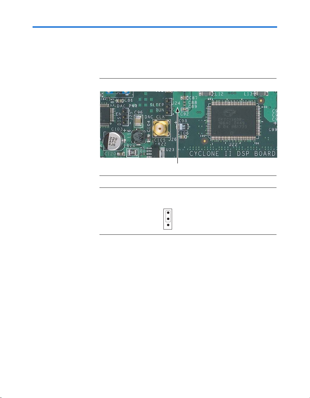
SSRAM Sleep & Run Modes (J24)
J24 selects SLEEP mode or RUN mode for the SSRAM. A jumper on pins
1 and 2 selects SLEEP mode, a jumper on pins 2 and 3 selects RUN mode,
as shown in Figure 2–13 and Figure 2–14.
Figure 2–13. SSRAM SLEEP & RUN Modes (J24)
Figure 2–14. Example of SSRAM in Sleep Mode
J24
SLEEP Mode
SLEEP
RUN
1
J24
3
EPCS Select (J29)
J29 selects the SAFE or USER EPCS configuration mode. See “EPCS64
Flash Memory Devices (U17, U36)” on page 38 for details on how to
configure SAFE and USER EPCS configuration modes.
Altera Corporation Reference Manual 2–37
August 2006 Cyclone II DSP Development Board
Page 46

Memory Components
EPCS64 Flash Memory Devices (U17, U36)
The Cyclone II DSP development board contains two EPCS64 flash
memory serial configuration devices (U17, U36) to configure the EP2C70
FPGA using the active serial (AS) configuration scheme.
Use the Quartus II software to program the EPCS64 devices (U17 and
U36) via the ASI connector (J13).
■ The EPCS64 device labeled U17 (SAFE EPCS) stores the factory
design. U17 is preprogrammed with the factory design; you can
reprogram U17 using the ASI interface. The EPCS64 device
configures the EP2C70 FPGA when J29 has a jumper on pins 1 and 2
and U17 contains valid data.
■ The EPCS64 device labeled U36 (USER EPCS) is provided to store a
user design. This device configures the EP2C70 FPGA when J29 has
a jumper on pins 2 and 3 and U36 contains valid data.
1 If there is no jumper on J29, the EPCS64 serial configuration
devices will not program the EP2C70 FPGA.
w The factory design in U17 may be overwritten. If this happens,
you can restore it as described in “Restoring the Factory Design”
on page D–1.
f For additional information about the EP2C70 FPGA, configuring
Cyclone II devices, the AS configuration scheme, and the ASMI, see the
following documents:
● Serial Configuration Devices (EPCS1, EPCS4, EPCS16, & EPCS64)
Features chapter in the Configuration Handbook, volume 2
● Active Serial Interface Data Sheet
● Configuring Altera FPGAs chapter in the Configuration Handbook,
volume 1
● Configuring Cyclone II Devices chapter in the Configuration
Handbook, volume 1
● Configuration & Testing chapter in the Cyclone II Device Handbook,
volume 2
● Configuring Cyclone II Devices chapter of the Cyclone II Device
Handbook, volume 6
2–38 Reference Manual Altera Corporation
Cyclone II DSP Development Board August 2006
Page 47
Cyclone II DSP Development Board Components
Synchronous SRAM Device (U22)
U22 is the synchronous SRAM (SSRAM), a Cypress Semiconductor
CY7C1360B-166 AC SSRAM device with a speed grade of 166 MHz on the
Cyclone II DSP development board. It is a 1 Mbyte pipelined
256 Kbit x 36-bit device in a 100-pin TQFP package.
1 The Cyclone II DSP development board only supports a 32-bit
interface due to pin-out constraints on the EP2C70F672.
1 Some of the SSRAM signal names were changed to facilitate
routing ease, reduce layer count, and improve signal integrity.
The method of addressing the SSRAM remains the same, but the
signal names from the EP2C70 have been changed and do not
necessarily match with the SSRAM chip signal names. For a
mapping of these signal names, see Appendix B, SSRAM
Pin-Out Table.
Table 2–22 lists the SSRAM device reference.
Table 2–22. SSRAM Device Reference
Item Description
Board reference U22
Part number CY7C1360B-166AC
Device description 9 Mbit, 256 Kbit x 36-bit/512 Kbit x 18 pipelined
Manufacturer Cypress Semiconductors
Manufacturer web site www.cypress.com
SSRAM
Altera Corporation Reference Manual 2–39
August 2006 Cyclone II DSP Development Board
Page 48
Memory Components
Table 2–23 lists the pin connections between the SSRAM and the
Cyclone II pin number.
Table 2–23. SSRAM Device Pin-Outs (Part 1 of 2) Note (1)
SSRAM Pin Name
A0 37 K26 DQC25 3 AB26
A1 36 E24 DQC26 6 AA25
A10 99 D25 DQC27 7 AA26
A11 43 K24 DQC28 8 AA24
A12 44 D23 DQC29 9 Y26
A13 45 J25 DQC30 12 W24
A14 46 C25 DQC31 13 U22
A15 47 G26 DQD16 18 V26
A16 48 C24 DQD17 19 U24
A17 49 E26 DQD18 22 U26
A18 38 E25 DQD19 23 T21
A19 39 F26 DQD20 24 R24
A2 82 L25 DQD21 25 P24
A20 42 GND DQD22 28 AB24
A3 33 H25 DQD23 29 N23
A4 81 L24 DQPA 51
A5 35 B25 DQPB 80
A6 100 E23 DQPC 1
A7 50 K25 DQPD 30
A8 34 D26 GW_n 88
A9 32 J26 MODE 31
ADSC_n 85 L20 NC_14 14
ADSP_n 84 N24 NC_16 16
ADV_n 83 M21 NC_66 66
BWA_n 93 F23 OE_n 86 AA23
BWB_n 94 M23 VDD 15
BWC_n 95 F25 VDD 41
BWD_n 96 M24 VDD 65
BWE_n 87 V23 VDD 91
SSRAM (U22)
Pin Number
Cyclone II
(U12) Pin
Number
SSRAM Pin Name
SSRAM (U22)
Pin Number
Cyclone II
(U12) Pin
Number
2–40 Reference Manual Altera Corporation
Cyclone II DSP Development Board August 2006
Page 49

Cyclone II DSP Development Board Components
Table 2–23. SSRAM Device Pin-Outs (Part 2 of 2) Note (1)
SSRAM Pin Name
CE1_n 98 J24 VDDQ 4
CE2 97 VDDQ 11
CE3_n 92 AE25 VDDQ 20
CLK 89 R25 VDDQ 27
DQA0 52 G24 VDDQ 54
DQA1 53 G23 VDDQ 61
DQA2 56 H24 VDDQ 70
DQA3 57 H23 VDDQ 77
DQA4 58 J23 VSS 17
DQA5 59 J22 VSS 40
DQA6 62 K23 VSS 67
DQA7 63 K22 VSS 90
DQB10 72 L21 VSSQ 5
DQB11 73 L19 VSSQ 10
DQB12 74 M20 VSSQ 21
DQB13 75 N20 VSSQ 26
DQB14 78 M19 VSSQ 55
DQB15 79 V22 VSSQ 60
DQB8 68 K21 VSSQ 71
DQB9 69 K19 VSSQ 76
SSRAM (U22)
Pin Number
Cyclone II
(U12) Pin
Number
SSRAM Pin Name
SSRAM (U22)
Pin Number
Cyclone II
(U12) Pin
Number
Note to Table 2–23:
(1) Blank cells indicate no connection.
Altera Corporation Reference Manual 2–41
August 2006 Cyclone II DSP Development Board
Page 50

Memory Components
Memory Mapping to the TMS320C6416 Digital Signal Processor
The Spectrum Digital DSP Starter Kit (DSK) for the TMS320C6416,
Revision E, featuring the TMS320C6416 digital signal processor,
interfaces with the Cyclone II DSP development board. This interface is
primarily used to memory map the EP2C70 FPGA to the TMS320C6416
processor address space allowing the Cyclone II DSP development board
to be used as n FPGA co-processor.
The SSRAM memory is bussed with connectors U34 and U40 to interface
with the TMS320C6416 board. The TMS320C6416 board brings out the
TMS320C6416’s External Memory Interface Connector (EMIF) memory
bus to two corresponding headers that connect to U34 and U40. See
“Expansion TI-EVM Connectors (U34, U40)” on page 2–47.
The TMS320C6416 processor memory maps to the Cyclone II DSP
development board’s SSRAM and EP2C70 FPGA with two chip select
signals on the TMS320C6416 processor:
■ EVM_CEn2 selects the SSRAM
■ EVM_CEn3 selects the EP2C70 FPGA
1 The SSRAM cannot be accessed by the EP2C70 FPGA while the
TMS320C6416 board is accessing the SSRAM via the TI-EVM
connector.
Because the SSRAM and EP2C70 FPGA device are bussed, there
is a single naming convention for the signals on the Cyclone II
DSP development board. These signals are named relative to the
TMS320C6416 board’s EMIF interface. For a mapping of these
signal names to signals used on the SSRAM, see Appendix B,
SSRAM Pin-Out Table.
2–42 Reference Manual Altera Corporation
Cyclone II DSP Development Board August 2006
Page 51
Cyclone II DSP Development Board Components
Expansion Connectors
This section describes the expansion connectors on the Cyclone II DSP
development board.
Expansion Prototype Connector (J15, J22 & J23)
J15, J22, and J23 are collectively called the Expansion Prototype
Connector, as shown in Figure 2–15. J15 is a 2x20 pin connector, while J22
is a 2x7 pin connector, and J23 is a 2x10 pin connector. These connectors
have 100-mil spacing between the pins and can be used for Altera
daughter cards or for debugging purposes.
Figure 2–15. Expansion Prototype Connector - J15, J22, & J23
J15Pin 1
Pin 1 Pin 1
J22 J23
Altera Corporation Reference Manual 2–43
August 2006 Cyclone II DSP Development Board
Page 52

Expansion Connectors
Figure 2–16 shows the Expansion Prototype Connector pin numbers.
Figure 2–16. Expansion Prototype Connector Pin Numbers - J15, J22 & J23
J15
GND
H6
F6
L7
J8
F4
G3
F2
F1
NC
GND
GND
GND
2
4
6
8
10
12
14
16
18
20
22
24
26
1
3
5
7
9
11
13
15
17
19
21
23
25
J5
A14
D2
PROTO_3_3V_5V
4
2
L6
G6
J7
6
K7
G5
J6
K4
J4
12
10
8
K8
14
G4
C2
D1
GND
G1
GND
2
J3
GND
4
H1
GND
6
GND
8
J2
28
27
J1
GND
30
29
K1
GND
10
M3
32
31
L2
GND
12
NC
34
33
M2
GND
14
H3
36
35
K3
GND
16
V2
38
37
G2
GND
18
GND
40
39
E2
GND
20
1
3
5
7
9
11
13
15
17
19
NC
3.3V
J22
1
GND
3
C3
3.3V
9
7
5
L3
K5
H4
13
11
L4
K6
DC_INPUT
(1)
PROTO_CLKIN (R20)
(3)
PROTO_CLKOUT (AD13)
3.3V
3.3V
3.3V
(4)
PROTO_CLK_OSC (U16 Pin 5)
(2)
J23
Notes to Figure 2–16:
(1) Voltage from DC power supply.
(2) Clock from the clock buffer U16.
(3) Clock from the EP2C70.
(4) Clock output from the card connected to the Expansion Prototype Connector.
2–44 Reference Manual Altera Corporation
Cyclone II DSP Development Board August 2006
Page 53
Cyclone II DSP Development Board Components
Table 2–24 lists the Expansion Prototype Connector pin numbers
Table 2–24. Expansion Prototype Connector Pin Numbers - J15, J22 & J23 (Part 1 of 3)
Cyclone II (U12) Signal
Name
PROTO_IO0 J5 B_PROTO_IO0 J15.3
PROTO_IO1 H6 B_PROTO_IO1 J15.4
PROTO_IO2 G6 B_PROTO_IO2 J15.5
PROTO_IO3 F6 B_PROTO_IO3 J15.6
PROTO_IO4 L6 B_PROTO_IO4 J15.7
PROTO_IO5 L7 B_PROTO_IO5 J15.8
PROTO_IO6 K7 B_PROTO_IO6 J15.9
PROTO_IO7 J8 B_PROTO_IO7 J15.10
PROTO_IO8 G5 B_PROTO_IO8 J15.11
PROTO_IO9 F4 B_PROTO_IO9 J15.12
PROTO_IO10 G4 B_PROTO_IO10 J15.13
PROTO_IO11 G3 B_PROTO_IO11 J15.14
PROTO_IO12 C2 B_PROTO_IO12 J15.15
PROTO_IO13 F2 B_PROTO_IO13 J15.16
PROTO_IO14 D1 B_PROTO_IO14 J15.17
PROTO_IO15 F1 B_PROTO_IO15 J15.18
PROTO_IO16 G1 B_PROTO_IO16 J15.21
PROTO_IO17 J3 B_PROTO_IO17 J15.23
PROTO_IO18 H1 B_PROTO_IO18 J15.25
PROTO_IO19 J1 B_PROTO_IO19 J15.27
PROTO_IO20 J2 B_PROTO_IO20 J15.28
PROTO_IO21 K1 B_PROTO_IO21 J15.29
PROTO_IO22 L2 B_PROTO_IO22 J15.31
PROTO_IO23 M3 B_PROTO_IO23 J15.32
PROTO_IO24 M2 B_PROTO_IO24 J15.33
PROTO_IO25 K3 B_PROTO_IO25 J15.35
PROTO_IO26 H3 B_PROTO_IO26 J15.36
PROTO_IO27 G2 B_PROTO_IO27 J15.37
PROTO_IO28 E2 B_PROTO_IO28 J15.39
PROTO_IO29 D2 B_PROTO_IO29 J22.4
PROTO_IO30 L3 B_PROTO_IO30 J22.5
Cyclone II (U12) Pin
Number
Proto Debug Signal Name Proto Debug Pin Number (1)
Altera Corporation Reference Manual 2–45
August 2006 Cyclone II DSP Development Board
Page 54

Expansion Connectors
Table 2–24. Expansion Prototype Connector Pin Numbers - J15, J22 & J23 (Part 2 of 3)
Cyclone II (U12) Signal
Name
PROTO_IO31 J7 B_PROTO_IO31 J22.6
PROTO_IO32 K5 B_PROTO_IO32 J22.7
PROTO_IO33 J4 B_PROTO_IO33 J22.8
PROTO_IO34 H4 B_PROTO_IO34 J22.9
PROTO_IO35 K4 B_PROTO_IO35 J22.10
PROTO_IO36 L4 B_PROTO_IO36 J22.11
PROTO_IO37 J6 B_PROTO_IO37 J22.12
PROTO_IO38 K6 B_PROTO_IO38 J22.13
PROTO_IO39 K8 B_PROTO_IO39 J22.14
PROTO_IO40 C3 B_PROTO_IO40 J22.1
Cyclone II (U12) Pin
Number
Proto Debug Signal Name Proto Debug Pin Number (1)
DC_INPUT J23.1
3.3V J23.5
3.3V J23.7
3.3V J23.15
3.3V J23.17
3.3V J23.19
GND J15. 2
GND J15.19
GND J15.22
GND J15.24
GND J15.26
GND J15.30
GND J15.40
GND J22.1
GND J23.2
GND J23.4
GND J23.6
GND J23.8
GND J23.10
GND J23.12
GND J23.14
GND J23.16
2–46 Reference Manual Altera Corporation
Cyclone II DSP Development Board August 2006
Page 55

Cyclone II DSP Development Board Components
Table 2–24. Expansion Prototype Connector Pin Numbers - J15, J22 & J23 (Part 3 of 3)
Cyclone II (U12) Signal
Name
PROTO_CLKIN R20 PROTO_CLKIN J23.11
PROTO_CLKOUT AD13 PROTO_CLKOUT J23.13
Note to Table 2–24:
(1) Unlisted pins have no connection.
Cyclone II (U12) Pin
Number
V2 B_PROTO_CARDSELn J15.38
Proto Debug Signal Name Proto Debug Pin Number (1)
GND J23.18
GND J23.20
B_PROTO_RESETn J15.1
PROTO_3_3V_5V J22.2
PROTO_CLK_OSC J23.9
Expansion TI-EVM Connectors (U34, U40)
The TI-EVM connectors connect to the EMIF connectors on the
TMS320C6416 board. U34 (labeled PERIPHERAL) and U40 (labeled
MEMORY) are located on the back of the Cyclone II DSP development
board.
The PERIPHERAL Interface (U34) on the Cyclone II DSP development
board connects to the External Peripheral Interface (J3) on the
TMS320C6416 board.
The MEMORY Interface (U40) on the Cyclone II DSP development board
connects to the External Memory Interface (J4) on the TMS320C6416
board.
Table 2–25 lists the TI-EVM connector pin-outs.
Table 2–25. TI-EVM Connector Pin-Outs (Part 1 of 4)
Schematic Signal
Name
EVM_A10 U40.16 D26
EVM_A11 U40.15 J26
EVM_A12 U40.14 D25
EVM_A13 U40.13 K24
EVM_A14 U40.10 D23
Altera Corporation Reference Manual 2–47
August 2006 Cyclone II DSP Development Board
TI-EVM Connector (U34, U40)
Pin Number
Cyclone II (U12) Pin
Number
Page 56
Expansion Connectors
Table 2–25. TI-EVM Connector Pin-Outs (Part 2 of 4)
Schematic Signal
Name
EVM_A15 U40.9 J25
EVM_A16 U40.8 C25
EVM_A17 U40.7 G26
EVM_A18 U40.6 C24
EVM_A19 U40.5 H25
EVM_A2 U40.26 E25
EVM_A20 U40.4 B25
EVM_A21 U40.3 F26
EVM_A3 U40.25 L24
EVM_A4 U40.24 E26
EVM_A5 U40.23 L25
EVM_A6 U40.20 E24
EVM_A7 U40.19 K26
EVM_A8 U40.18 E23
EVM_A9 U40.17 K25
EVM_ARDY U40.76 W23
EVM_AREN U40.73 P26
EVM_AWEN U40.74 V23
EVM_BEN0 U40.30 F23
EVM_BEN1 U40.29 M23
EVM_BEN2 U40.28 F25
EVM_BEN3 U40.27 M24
EVM_CEN2 U40.78 J24
EVM_CEN3 U40.77 AE25
EVM_CLKOUT2 U34.78 P2
EVM_CLKR0 U34.27 G25
EVM_CLKX0 U34.21 F24
EVM_CNTL0 U34.64 M21
EVM_D0 U40.70 V22
EVM_D1 U40.69 AB25
EVM_D10 U40.58 L21
EVM_D11 U40.57 Y26
TI-EVM Connector (U34, U40)
Pin Number
Cyclone II (U12) Pin
Number
2–48 Reference Manual Altera Corporation
Cyclone II DSP Development Board August 2006
Page 57

Cyclone II DSP Development Board Components
Table 2–25. TI-EVM Connector Pin-Outs (Part 3 of 4)
Schematic Signal
Name
EVM_D12 U40.56 K19
EVM_D13 U40.55 W24
EVM_D14 U40.54 K21
EVM_D15 U40.53 U22
EVM_D16 U40.50 K22
EVM_D17 U40.49 V26
EVM_D18 U40.48 K23
EVM_D19 U40.47 U24
EVM_D2 U40.68 M19
EVM_D20 U40.46 J22
EVM_D21 U40.45 U26
EVM_D22 U40.44 J23
EVM_D23 U40.43 T21
EVM_D24 U40.40 H23
EVM_D25 U40.39 R24
EVM_D26 U40.38 H24
EVM_D27 U40.37 P24
EVM_D28 U40.36 G23
EVM_D29 U40.35 AB24
EVM_D3 U40.67 AB26
EVM_D30 U40.34 G24
EVM_D31 U40.33 N23
EVM_D4 U40.66 N20
EVM_D5 U40.65 AA25
EVM_D6 U40.64 M20
EVM_D7 U40.63 AA26
EVM_D8 U40.60 L19
EVM_D9 U40.59 AA24
EVM_DMAC0 U34.74 N24
EVM_DR0 U34.30 H26
EVM_DX0 U34.24 G21
EVM_FSR0 U34.29 J20
TI-EVM Connector (U34, U40)
Pin Number
Cyclone II (U12) Pin
Number
Altera Corporation Reference Manual 2–49
August 2006 Cyclone II DSP Development Board
Page 58

General Connectors
Table 2–25. TI-EVM Connector Pin-Outs (Part 4 of 4)
General
Connectors
Schematic Signal
Name
EVM_FSX0 U34.23 G22
EVM_IACK U34.54 N26
EVM_INT0 U34.53 M22
EVM_INT1 U34.48 M25
EVM_INT2 U34.67 AC26
EVM_INT3 U34.68 L23
EVM_INUM0 U34.58 P1
EVM_OEN U40.75 AA23
EVM_RESET U34.59 P25
EVM_STAT0 U34.66 L20
This section describes the general connectors on the Cyclone II DSP
development board.
TI-EVM Connector (U34, U40)
Pin Number
Cyclone II (U12) Pin
Number
JTAG Connector (J9)
The Cyclone II DSP development board contains one JTAG connector (J9).
This connector provides communication between a PC running the
Quartus II software and the Cyclone II DSP development board. The pins
on J9 are connected to J12 through 0-Ω series resistors, and care must be
taken so that signal contention does not occur between the two
connectors.
The EP2C70 can be programmed with the JTAG interface. A JTAG UART
megafunction is also provided on the Nios
Evaluation Edition, version 6.0.1 CD-ROM for designers to instantiate in
their design as well as a host-side (PC-side) API for transferring data
using scripts or compiled programs. You can reach speeds up to 1 Mbps.
Nios or Nios II based programmable logic device (PLD) designs can use
this interface to control and/or download code.
2–50 Reference Manual Altera Corporation
Cyclone II DSP Development Board August 2006
®
II Embedded Processor
Page 59

Cyclone II DSP Development Board Components
Table 2–26 lists the JTAG connector pin-outs.
Table 2–26. JTAG Connector Pin-Outs
Schematic Signal Name JTAG Connector (J9) Pin Number
JTAG_TCK 1
GND 2
GND 10
3.3V 4
3.3V 6
JTAG_CONN_TDI 3
JTAG_TMS 5
JTAG_CONN_TDO 9
Altera Corporation Reference Manual 2–51
August 2006 Cyclone II DSP Development Board
Page 60

General Connectors
Active Serial Interface (ASI) Connector (J13)
The active serial interface (ASI) connector is used to program the EPCS64,
U17 and U36, using the Quartus II software. See Figure 2–17.
For more information about using J13, see “EPCS64 Flash Memory
Devices (U17, U36)” on page 2–38.
Figure 2–17. Active Serial Interface Connector With JTAG Cable to Program the
EPCS64 Flash Memory
JTAG Cable
2–52 Reference Manual Altera Corporation
Cyclone II DSP Development Board August 2006
J13
ASI Connector
Page 61
Cyclone II DSP Development Board Components
Mictor Connector (J12)
The Mictor connector (J12) can be used to transmit up to 27 high-speed
I/O signals with very low noise via a shielded Mictor cable. J12 is used as
a hardware or software debug port.
Table 2–27 lists the Mictor connector references.
Table 2–27. Mictor Connector Reference
Item Description
Board reference J12
Part number 2-767004-2
Device description Mictor connector
Manufacturer AMP
Manufacturer web site www.amp.com
The Mictor connector signals are allocated as follows:
■ Twenty-five data signals
■ One clock input signal
■ One clock output signal
Pin allocation is shown in Figure 2–19 on page 2–54 and listed in
Table 2–28. Most of the pins on J12 connect to the I/O pins on the EP2C70.
For systems that do not use the Mictor connector for debugging the
Nios II processor, any on-chip signals can be routed to I/O pins and
probed at the Mictor connector (J12) via a Mictor cable.
You can also connect external scopes and logic analyzers to J12 to analyze
large number of signals simultaneously.
f For details on Nios II debugging products that use the Mictor connector,
select the Nios II link on Literature section of the Altera Web site at
www.altera.com.
c The JTAG signals have special usage requirements. You cannot
use J12 and J9 at the same time.
Altera Corporation Reference Manual 2–53
August 2006 Cyclone II DSP Development Board
Page 62

General Connectors
Figure 2–18 shows the connections from the Mictor connector to the
EP2C70 FPGA and the JTAG connector.
Figure 2–18. Mictor Connector Signaling
Mictor Connector
J12
Figure 2–19 shows the J12 pin-outs to the EP2C70. Unless otherwise
noted, labels indicate EP2C70 pin numbers.
Figure 2–19. Mictor Connector (J12) Pin-Outs
37 D1
39 GND (3)
41 GND (3)
43 GND (3)
35 F1
33 G1
31 J3
29 H1
27 J1
JTAG Connector
J9
4
40
25 J2
23 K1
21 NC
19 (1)
17 (1)
15 (1)
EP2C35F672
(U12)
13 L2
11 (1)
9 M3
7 M2
5 (1)
3 NC
1 NC
42 GND (3)
36 H6
34 G6
32 F6
30 L6
28 L7
26 K7
24 J8
22 G5
20 F4
18 G4
16 G3
14 3.3 V (2)
12 3.3 V (2)
10 C2
8 F2
6 (1)
4 NC
2 NC
38 J5
40 GND (3)
Notes to Figure 2–19:
(1) Pins 5, 6, 11, 15, 17, and 19 are not connected to the EPC335 FPGA.
(2) Pins 12 and 14 are at 3.3V.
(3) Pins 39 through 43 are GND.
2–54 Reference Manual Altera Corporation
Cyclone II DSP Development Board August 2006
Page 63

Cyclone II DSP Development Board Components
Table 2–28 lists the Mictor connector pin-outs.
Table 2–28. Table 23 Mictor Connector to Cyclone II Pinout (Part 1 of 2)
Cyclone II (U12) Pin Number Mictor (J12) Debug Signal Name Mictor (J12) Debug Pin Number
J5 PROTO_IO0 38
H6 PROTO_IO1 36
G6 PROTO_IO2 34
F6 PROTO_IO3 32
L6 PROTO_IO4 30
L7 PROTO_IO5 28
K7 PROTO_IO6 26
J8 PROTO_IO7 24
G5 PROTO_IO8 22
F4 PROTO_IO9 20
G4 PROTO_IO10 18
G3 PROTO_IO11 16
C2 PROTO_IO12 10
F2 PROTO_IO13 8
D1 PROTO_IO14 37
F1 PROTO_IO15 35
G1 PROTO_IO16 33
J3 PROTO_IO17 31
H1 PROTO_IO18 29
J1 PROTO_IO19 27
J2 PROTO_IO20 25
K1 PROTO_IO21 80
L2 PROTO_IO22 13
M3 PROTO_IO23 9
M2 PROTO_IO24 7
GND 39
GND 40
GND 41
GND 42
GND 43
3.3V 12
Altera Corporation Reference Manual 2–55
August 2006 Cyclone II DSP Development Board
Page 64

General Connectors
Table 2–28. Table 23 Mictor Connector to Cyclone II Pinout (Part 2 of 2)
Cyclone II (U12) Pin Number Mictor (J12) Debug Signal Name Mictor (J12) Debug Pin Number
3.3V 14
MICTOR_PLDCLK 5
MICTOR_TR_CLK 6
MICTOR_TDO 11
MICTOR_TCK 15
MICTOR_TMS 17
MICTOR_TDI 19
3.3V 12
3.3V 14
Note to Table 2–28:
(1) Blank cells indicate no connection.
2–56 Reference Manual Altera Corporation
Cyclone II DSP Development Board August 2006
Page 65
Cyclone II DSP Development Board Components
Status LEDs & Reset/Power Switches
This section describes the status LEDs and reset switches on the
Cyclone II DSP development board. Some of the switches are userdefined.
Power (D1) & Status (D10) LEDs
The power LED (D1) turns on indicating that voltage is supplied to the
DC jack, J1, and is being distributed to the Cyclone II DSP development
board’s on-board power regulators. For information about powering up
the Cyclone II DSP development board, see “Power Switch (SW1)” on
page 2–57.
The Cyclone II DSP development board has one CONF DONE LED (D10)
that turns on to indicate successful configuration of the EP2C70 FPGA.
This LED is driven by the EP2C70(U12), pin R23 (CONF_DONE). See
Table 2–29.
Table 2–29. Status & Power LEDs Pin-Outs
LED Name Schematic Signal Name Description
D1
D10
DC_IN
EP2C_CONFIG_DONE
DC Input Power OK
Cyclone II DSP development board
successfully configured
Power Switch (SW1)
SW1 is a power switch that connects the 9-20 V DC input from the DC
power jack, J1, to the on-board power regulators. When SW1 is in the ON
position, LED (D1) turns on.
User Defined Reset (SW6) Push-Button
SW6 is a USER RESET momentary-contact push button. It is used as
defined by the user, and could be used for initialization and reset of a user
design running on the Cyclone II DSP development board. This button
must first be defined by the user before it can be used. See Table 2–30.
Altera Corporation Reference Manual 2–57
August 2006 Cyclone II DSP Development Board
Page 66
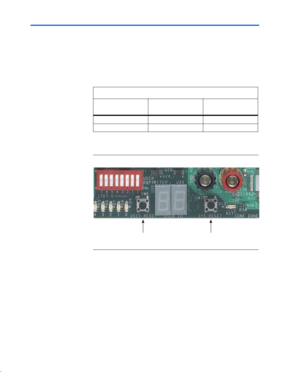
Status LEDs & Reset/Power Switches
System Reset (SW7) Push-Button
SW7 is a SYS RESET momentary-contact push button. When pressed, it
resets the hardware and programs the EP2C70 FPGA with the design
stored in the EPCS64 device. The EPCS64 (U17) device is preprogrammed
with the factory design but you can overwrite the factory
preprogramming. See Table 2–30.
Table 2–30. SW6 & SW7 Push-Button Pin-Outs
Push-button Schematic Signal Name
SW6 (user-defined)
SW7
USER_RESETn A14
SYS_RESETn N7
Figure 2–20 shows the locations of SW6 and SW7.
Figure 2–20. SW6 USER RESET & SW7 SYS RESET
SW6
USER RESET
Cyclone II (U12) Pin
Number
SW7
SYS RESET
2–58 Reference Manual Altera Corporation
Cyclone II DSP Development Board August 2006
Page 67
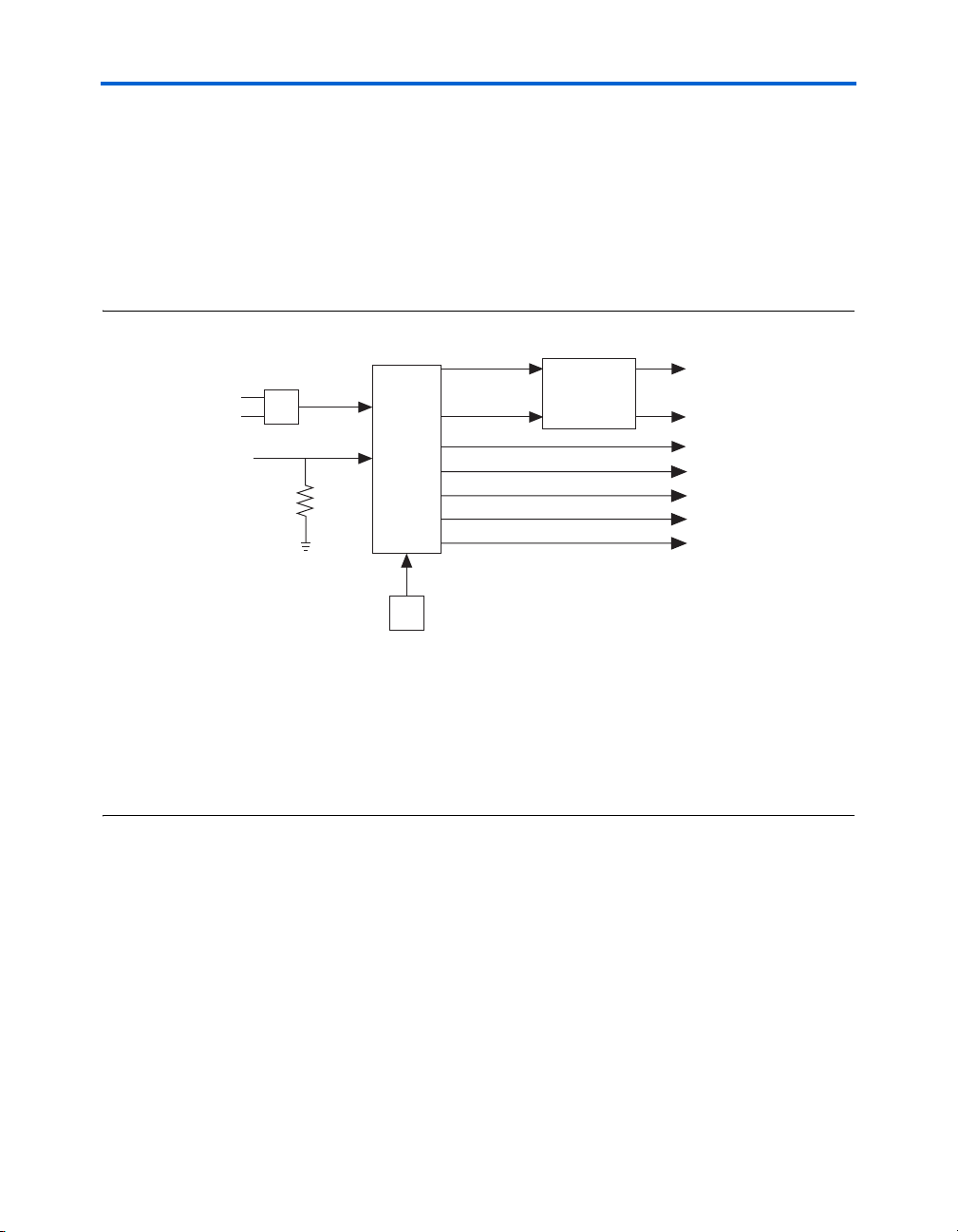
Cyclone II DSP Development Board Components
)
Clock Circuitry
This section describes the components used to set the Cyclone II DSP
development board clocking options.
Figure 2–21 shows the clock distribution on Cyclone II DSP development
board. The clocks must be defined first, this occurs within U16, the clock
buffer, which generates eight identical clock outputs (one output is
unconnected and two outputs are unused) used throughout the
Cyclone II DSP development board. See “Clock Buffer (U16)”.
Figure 2–21. Cyclone II DSP Development Board Clocking Options
CLKIN_TOP
Custom Clock (J20)
On-Board Clock (U20)
SMA External Clock (J17)
J18
CMOS
LVTTL
RT
U16
Clock
Buffer
J19
CLKIN_BOT
U12
EP2C35
Notes to Figure 2–21:
(1) This signal is input to J35 as the FPGA clock (FPGA_TO_DAC_CLK). See “D/A Converter Clocks” on page 2–18.
(2) This signal is input to J37 as the FPGA clock (FPGA_TO_ADC_CLK). See “A/D Converter Clocks” on page 2–23.
(3) This signal is input to J23 as the PROTO clock (PROTO_CLK_OSC). See Figure 2–16 on page 2–44.
(4) This signal is input to J35 as the OSC clock (CLK_OSC_DACA). See “D/A Converter Clocks” on page 2–18.
(5) This signal is input to J37 as the OSC clock (CLK_OSC_ADCA). See “A/D Converter Clocks” on page 2–23.
(6) This signal is input to J34 as the OSC clock (CLK_OSC_DACB). See “D/A Converter Clocks” on page 2–18.
(7) This signal is input to J36 as the OSC clock (CLK_OSC_ADCB). See “A/D Converter Clocks” on page 2–23.
FPGA Clock to DAC
FPGA Clock to ADC
PROTO OSC Clock Out
DAC A Clock Out
ADC A Clock Out
DAC B Clock Out
ADC B Clock Out
(1)
(2)
(4)
(5)
(6)
(7)
(3
Altera Corporation Reference Manual 2–59
August 2006 Cyclone II DSP Development Board
Page 68

Clock Circuitry
r
(
)
Setting the Clocks
The clocks are selected from one of the following clock sources (as shown
in Figure 2–21):
■ The on-board clock oscillator (U20)
■ The custom clock oscillator (J20)
■ The SMA connector (J17)
The following two jumpers select the clock outputs from the clock buffer
(U16). (see Table 2–31):
1. J18 selects U20 or J20 as the selected clock oscillator to be input to
U16.
2. J19 determines which input to U16 (the selected clock oscillator or
the SMA clock), will be used to output the clocks.
Figure 2–22 shows U20, the on-board 100 MHz clock oscillator (it is
mounted in the gray area as the arrow indicates. If a custom clock
oscillator is used, it is installed on the blue socket (J20), as the arrow
indicates, on top of U20. Figure 2–22 also shows J18 and J19.
Figure 2–22. U20/J20, J18 & J19
J18
2–60 Reference Manual Altera Corporation
Cyclone II DSP Development Board August 2006
J19
U20 - On-Board
100 MHz Oscillator
Socket to Mount J20 - Custom Oscillato
Mounts on Top of U20
Page 69

Cyclone II DSP Development Board Components
Figure 2–23 shows J18 and J19 with sample jumpers placed on pins 1 and
2. This setting selects the on-board clock oscillator as the input to U16.
Figure 2–23. J18 & J19 Pin-Outs
Table 2–31 lists the setting on J18 and J19 that select desired input to be
input to U16
Table 2–31. Selecting the Clock Input to U16
Clocking Option Settings
On-board clock oscillator (U20) ● On J18, place a jumper on pins 1 and 2.
Custom oscillator (J20)
SMA connector (J17)
1
SMT OSC
J18
SKT OSC
3
1
OSC
J19
SMA
3
● On J19, place a jumper on pins 1 and 2.
● Plug a custom half-can oscillator into the
J20 socket.
● On J18, place a jumper on pins 2 and 3.
● On J19, place a jumper on pins 1 and 2.
● Use J17 (CLK_SMA) for external clock
input.
● On J19, place a jumper on pins 2 and 3.
CLK SMA Connector (J17)
The CLK SMA connector (J17) provides an external clock input. It can be
selected to be the input to U16. J17 is shown in Figure 2–4 on page 2–11.
An external clock source provides designers, while using a particular
design, the flexibility to alter the input frequency to verify F
MAX
tolerances.
On-Board/Custom Clock Oscillators Select Jumper (J18)
J18 selects the on-board clock oscillator (U20) or the custom clock
oscillator (J20) as the selected clock oscillator to be input to U16. See
Figure 2–22 and Figure 2–23.
Altera Corporation Reference Manual 2–61
August 2006 Cyclone II DSP Development Board
Page 70

Clock Circuitry
Clock Select Jumper (J19)
J19 determines which input to U16 (the selected clock oscillator or the
SMA clock will be used to determine the clock outputs of U16. See
Figure 2–22 and Figure 2–23.
Socket for a Custom Clock Oscillator (J20)
J20 is a socket for connecting a half-can oscillator that can be used instead
of the on-board clock oscillator (U20). An oscillator inserted into J20 is
called the custom clock and is not included in the DSP Development Kit,
Cyclone II Edition. The custom oscillator can be selected to be the input to
U16.The J20 socket is mounted on top of U20, the on-board clock
oscillator, as shown in Figure 2–22.
D/A Converter CLK SMA Connector (J26)
J26 is an SMA connector that provides an external clock input to the D/A
converter. It can be selected to be the D/A converter clock. See “D/A
Converter Clocks” on page 2–18. J26 is shown in Figure 2–7 on page 2–18.
Table 2–12 on page 2–19 describes the D/A converter clock source
settings.
A/D Converter CLK SMA Connector (J27)
J27 is an SMA connector that provides an external clock input to the A/D
converter. It can be selected to be the A/D clock. See “A/D Converter
Clocks” on page 2–23. J27 is shown in Figure 2–10 on page 2–23.
Table 2–17 on page 2–24 describes the A/D converter clock source
settings.
D/A Converter CLK Select Jumper (J35 & J34)
J35 is used to choose between three clocking inputs to select the
DAC CHANNEL A clock. J34 is used to choose between three clocking
inputs to select the DAC CHANNEL B clock. The J35 and J34 D/A
converter clock select settings are described in Table 2–12 on page 2–19.
J35 and J34 are shown in Figure 2–7 on page 2–18.
A/D Converter CLK Select Jumper (J37 & J36)
J37 is used to choose between three clocking inputs to select the
ADC CHANNEL A clock. J36 is used to choose between three clocking
inputs to select the ADC CHANNEL B clock.The J37and J36 A/D
converter clock select settings are described in Table 2–17 on page 2–24.
J37 and H36 are shown in Figure 2–10 on page 2–23.
2–62 Reference Manual Altera Corporation
Cyclone II DSP Development Board August 2006
Page 71

Cyclone II DSP Development Board Components
D/A Converter Power Select Jumper (J33)
J33 determines whether the D/A converter is powered at 3.3 volts or 5
volts. When the jumper is on pins 2 and 3, the D/A converter is powered
at 3.3 volts. When the jumper is on pins 1 and 2., the D/A converter is
powered at 5 volts.
Clock Buffer (U16)
U16 generates the clocks used on the Cyclone II DSP development board.
U16 generates seven identical clock outputs that carry clock signals to
other components on the Cyclone II DSP development board. The clock
buffer is a low-skew, single-input to eight-output clock buffer (one output
is unconnected and two outputs are unused). Table 2–32 lists the U16 pin-
outs.
Table 2–32. Clock Buffer Distribution
Clock Buffer
Output Pin (U16)
U16.3 U12.N2
U16.4 U12.N25
U16.5 J23.9
U16.11 J37.1
U16.13 J35.1
U16.12 J36.1
U16.14 J34.1
Destination Description
Cyclone II
Cyclone II
Expansion Prototype Connector
A/D converter Channel A Clock Select
D/A CONVERTER Channel A Clock Select
A/D converter Channel B Clock Select
D/A CONVERTER Channel B Clock Select
On-Board Clock Oscillator (U20)
The on-board clock oscillator is a 100-MHz free-running oscillator that
can be used as an input to U16.
Altera Corporation Reference Manual 2–63
August 2006 Cyclone II DSP Development Board
Page 72

Powe r S up ply
Table 2–33 lists the on-board oscillator reference.
Table 2–33. On-Board Oscillator Reference
Item Description
Board reference U20
Part number ECS-3953M-1000-BN-TR
Device description 100-MHz surface mount oscillator
Manufacturer ECS, Inc.
Manufacturer web site www.ecsxtal.com
Power Supply
This section describes the power supply, power regulators, and the power
plane connectors.
DC Power Input Jack (J1)
A 9-20 Volt (V) DC input is provided by a right-angle 2.5 mm power jack
with a 5.5mm barrel. Two switching power supplies are used to provide
the incoming DC voltage, which is regulated down to 6 V, 3.3 V, and 1.8 V
by three switching power supplies. From these voltages all other onboard voltages are generated.
Table 2–34 lists the power-supply specifications.
Table 2–34. Power Supply Specifications
Item Description
Board reference N/A (power supply adapter)
Part number TR9KT3750LCP-Y
Device description Switching power supply,
Input: 100-240 V, ~1.2 A max., 50-60 Hz
Output: +16 V, 3.75 A, 60 W max.
Manufacturer GlobTek Inc.
Manufacturer web site www.globtek.com
2–64 Reference Manual Altera Corporation
Cyclone II DSP Development Board August 2006
Page 73

Cyclone II DSP Development Board Components
Cyclone II DSP Development Board Power-Up
The Cyclone II DSP development board can be powered up in two ways:
■ 9-20 V DC power input jack (J1).
■ Bench power supplies (banana jacks), which requires removing fuses
to isolate the bench power supplies from the on-board regulators. See
“Bench Power Supplies Using Banana Jacks” on page 2–67.
c Before you connect a bench power supply, remove fuses on the
Cyclone II DSP development board. All fuses are LITTLEFUSE
154 007 and are 7 A. The fuses do not protect the board from
power surges.
f For additional information about connecting cables and powering up the
Cyclone II DSP development board, see the Connecting the Cables to the
Board and PC section in the DSP Development Kit, Cyclone II Edition Getting
Started Guide.
Voltage Limiter Switches (U13-U15, U18 & U19)
Each signal passes through analog switches to protect the EP2C70 from 5V logic levels. Analog switches are permanently enabled. These voltage
limiters combine with J15, J22, and J23, which make up the Expansion
Prototype Connector. See “Expansion Prototype Connector (J15, J22 &
J23)” on page 2–43 and “Power Supply” on page 2–65.
Altera Corporation Reference Manual 2–65
August 2006 Cyclone II DSP Development Board
Page 74

Powe r S up ply
On-Board Power Regulators (U2, U7, U8, U9, U10, U23 & U24)
There are seven voltage regulators on the Cyclone II DSP development
board to control eight separate voltage rails. Two switching regulators
provide 3.3 V, 1.8 V, and 6 V. Five linear regulators provide 5 V, 1.2 V,
0.9 V, VCCA_DAC, and VCCA_ADC. Table 2–35 describes each voltage
regulator. See Figure 2–24 for the locations of the voltage regulators on
the Cyclone II DSP development board.
Table 2–35. Cyclone II DSP Development Board Regulators
Board
Reference
U2
U7
U8
U9
U10
U23
U24
Type
Dual
output
switching
regulator
Linear
regulator
Linear
regulator
Switching
regulator
Linear
regulator
Linear
regulator
Linear
regulator
Voltage
Output
3.3 V
1.8 V
1.2 V ● Cyclone II VCCINT
● Cyclone II VCCIO banks 1, 2, 5, and 6
● Clock oscillators and buffers
● Expansion Prototype Connector
● SSRAM
● EPCS64
● LEDs and seven-segment displays
● DIP switches and push-buttons
● Audio CODEC
● Video DAC
● DDR2 SDRAM DIMM
● Cyclone II VCCIO banks 3, 4, 7, and 8
● VCCA_PLL
● VCCD_PLL
Provides Power To Manufacturer Part Number
Texas
Instruments
TPS51020
TPS51020
UC382TD
0.9 V ● DDR2 SDRAM VTT TPS51100
6V ● VCCA_ADC regulator
● VCCA_DAC regulator
5V ● Linear 0.9V regulator
● Expansion Prototype Connector card
TPS40055
REG104GA
voltage limiters
3.3 V
● D/A Converter voltage REG104GA
5V
3.3 V ● A/D Converter voltage REG104GA
2–66 Reference Manual Altera Corporation
Cyclone II DSP Development Board August 2006
Page 75

Cyclone II DSP Development Board Components
Bench Power Supplies Using Banana Jacks
Socketed fuses are provided to isolate the voltage planes from the
regulators to allow bench supplies to power these sections using banana
jacks. The bench supply inputs are placed after the other power supplies
(whether linear or switching supplies) on the Cyclone II DSP
development board in order to allow current draw measurements.
Figure 2–24 shows a block diagram of the power supply generation and
distribution.
c Before you connect a bench power supply, remove fuses on the
Cyclone II DSP development board. All fuses are LITTLEFUSE
154 007 and are 7 A. The fuses do not protect the board from
power surges.
Altera Corporation Reference Manual 2–67
August 2006 Cyclone II DSP Development Board
Page 76
Powe r S up ply
Figure 2–24. Cyclone II DSP Development Board Power Distribution Diagram
DC Input
(40W)
(v8 03/18/05)
J2
Digital Ground
J40
DAC Ground
J41
ADC Ground
3.3V
U2
Dual
Output
Switching
Regulator
1.8V
U9
Switching
Regulator
J4
3.3V 3.3V
7A
F3
(1)
J3
1.8V
7A
(1)
6V
1.5A
(1)
1.8V
1.8V
Voltage
Select
F2
3.3V
U7
Linear
Regulator
1.2V
U23
Linear
Regulator
5.5V/3.3V
U24
Linear
Regulator
3.3V
U8
Linear
Regulator
0.9V
3A
(1)
1A
(1)
1A
(1)
J6
F4
200mA
J5
F1
J39
F6
J42
F7
1.8V
VTT_DIMM
(1)
3A
VREF_DIMM
Passive
Filters
VCCA_DAC
VCCA_ADC
Single 3.3V Plane
DDR2 SDRAM DIMM
VCCA_PLL1
VCCA_PLL2
VCCA_PLL3
VCCA_PLL4
Single 1.2V Plane
DAC Analog Plane
ADC Analog Plane
U10
Linear
Regulator
5V
1A
(1)
F5
5V
(1) Regulators can source up to the indicated current.
2–68 Reference Manual Altera Corporation
Cyclone II DSP Development Board August 2006
Page 77

Cyclone II DSP Development Board Components
Power Plane Connectors (J2-J6, J39 Through J42)
Bench power supplies provide an easy way to measure the current draw
on each power plane. When one plane is being powered by the bench
supply, all other planes still draw current from the DC power input. Upon
applying power to the Cyclone II DSP development board, the power
LED (D1) should be on.
Table 2–36 lists the procedure for powering individual planes through
bench power supplies. In the instructions, only remove the fuse listed in
the Settings column. Other fuses should be left on Cyclone II DSP
development board.
Table 2–36. Procedure for Powering Individual Power Planes Through Bench Power Supplies (Part 1 of 2)
Power Plane
3.3V
1.8V
6V
1.2V
5V
VTT
Power Plane Using Bench Power
Supplies
Cyclone II VCCIO banks 1, 2, 5, and 6,
clock oscillators and buffers, Expansion
Prototype Connector, SSRAM,
EPCS64, LEDs, Audio CODEC, Video
DAC, translators
DDR2 DIMM, Cyclone II VCCIO, banks
3, 4, 7, and 8
VCCA_ADC regulator, VCCA_DAC
regulator
Cyclone II VCCINT, VCCA_PLL, and
VCCD_PLL
Expansion Prototype Connector card
voltage limiters
DDR2 VTT power ● Remove fuse F4
● Remove fuse F3
● Apply 3.3 V to J4
● Apply GND to J2
● Remove fuse F2
● Apply 1.8 V to J3
● Apply GND to J2
There is no on-board provision to apply 6 V externally
or to remove the regulator from the circuit.
● Remove fuse F1
● Apply 1.2 V to J5
● Apply GND to J2
● Remove fuse F5
● Place a jumper on pins 2 and 3 on J7 to disable the
regulator.
There is no on-board provision to apply 5 V externally.
● Apply 0.9 V to J6
● Apply GND to J2
Settings
Altera Corporation Reference Manual 2–69
August 2006 Cyclone II DSP Development Board
Page 78

Powe r S up ply
Table 2–36. Procedure for Powering Individual Power Planes Through Bench Power Supplies (Part 2 of 2)
Power Plane
VCCA_ADC
VCCA_DAC
Power Plane Using Bench Power
Supplies
A/D converter power ● Remove fuse F7
● Place a jumper on pins 2 and 3 on J28 to disable the
regulator
● Apply 3.3 V to J42
● Apply GND to J41
D/A converter power ● Remove fuse F6
● Place a jumper on pins 2 and 3 on J25 to disable the
regulator
● Apply 5 V to J39 and GND to J40
or
● Apply 3.3 V to J39 and GND to J40
Settings
2–70 Reference Manual Altera Corporation
Cyclone II DSP Development Board August 2006
Page 79

Appendix A. DDR2 SDRAM
DIMM Connector Pin Out Table
Introduction
The printed circuit board (PCB) layout for the DDR2 SDRAM DIMM
interface to the Cyclone™ II EP2C70 FPGA was optimized for a reduced
layer count, reduced via count, and improved signal integrity. This
required swapping names from the pin locations created by the DDR2
®
MegaCore
function’s placement and pin-out tool command language
(Tcl) script. These swaps only occurred within each octal byte lane (for
example, DQ0-DQ7). The result is that, for example, a DDR2 SDRAM
®
DIMM FPGA design in the Quartus
II software will have an I/O called
DIMM_DQ0 (data bit 0) but the corresponding net name on the schematic
that this logical pin is connected to is called DIMM_DQ7 (data bit 7).
Conversely, the DIMM_DQ7 bit is driven to net named DIMM_DQ0. This
swapping list is provided in Tab l e A –1 .
Use the DDR2 MegaCore function’s default pinout script location for the
EP2C70F672 interface width and do not re-assign the pins to match the
Cyclone II DSP development board’s signal names as DQ data pins. Use
Ta bl e A –1 if you need to track a particular signal to its destination for
eye-diagrams or for general debugging purposes.
Table A–1. Cyclone II EP2C70F672 DSP Development Board to DIMM Pin Changes (Part 1 of 4)
Signal Name Original DDR2 Core Location
DIMM_DQ0 AD16 AA16
DIMM_DQ1 AF17 AC17
DIMM_DQ2 AE17 AE17
DIMM_DQ3 AC17 AF17
DIMM_DQ4 AD17 Y16
DIMM_DQ5 AA16 AD17
DIMM_DQ6 Y16 AF18
DIMM_DQ7 AF18 AD16
DIMM_DQ8 AD12 Y15
DIMM_DQ9 AE12 AA15
DIMM_DQ10 AC14 AC14
DIMM_DQ11 AA13 AD12
DIMM_DQ12 Y13 Y13
EP2C70F672 Board
Location
Ye s
Ye s
No
Ye s
Ye s
Ye s
Ye s
Ye s
Ye s
Ye s
No
Ye s
No
Different
(Yes/No)
Altera Corporation Reference Manual A–1
August 2006 Preliminary
Page 80

Introduction
Table A–1. Cyclone II EP2C70F672 DSP Development Board to DIMM Pin Changes (Part 2 of 4)
Signal Name Original DDR2 Core Location
DIMM_DQ13 Y14 Y14
DIMM_DQ14 Y15 AA13
DIMM_DQ15 AA15 AE12
DIMM_DQ16 AE9 AC11
DIMM_DQ17 AF9 AD10
DIMM_DQ18 AD10 AE10
DIMM_DQ19 AC11 AE9
DIMM_DQ20 AE10 AB12
DIMM_DQ21 AF10 AD11
DIMM_DQ22 AB12 AF10
DIMM_DQ23 AD11 AF9
DIMM_DQ24 AE6 AB10
DIMM_DQ25 AF6 AA10
DIMM_DQ26 AA9 AE6
DIMM_DQ27 AA10 AE7
DIMM_DQ28 AB10 Y11
DIMM_DQ29 AA11 AA11
DIMM_DQ30 Y11 AF6
DIMM_DQ31 AE7 AA9
DIMM_DQ32 F11 F11
DIMM_DQ33 C9 D8
DIMM_DQ34 D9 C8
DIMM_DQ35 G10 D9
DIMM_DQ36 F10 G10
DIMM_DQ37 C8 F10
DIMM_DQ38 D8 A7
DIMM_DQ39 A7 C9
DIMM_DQ40 F12 B10
DIMM_DQ41 D12 A10
DIMM_DQ42 E12 F12
DIMM_DQ43 G11 G11
DIMM_DQ44 A10 D10
EP2C70F672 Board
Location
Different
(Yes/No)
No
Ye s
Ye s
Ye s
Ye s
Ye s
Ye s
Ye s
Ye s
Ye s
Ye s
Ye s
Ye s
Ye s
Ye s
Ye s
No
Ye s
Ye s
No
Ye s
Ye s
Ye s
Ye s
Ye s
Ye s
Ye s
Ye s
Ye s
Ye s
No
Ye s
A–2 Reference Manual Altera Corporation
Cyclone II DSP Development Board August 2006
Page 81
Table A–1. Cyclone II EP2C70F672 DSP Development Board to DIMM Pin Changes (Part 3 of 4)
Signal Name Original DDR2 Core Location
DIMM_DQ45 B10 C10
DIMM_DQ46 D10 D12
DIMM_DQ47 C10 E12
DIMM_DQ48 B16 F14
DIMM_DQ49 B15 D14
DIMM_DQ50 C15 B16
DIMM_DQ51 G13 G14
DIMM_DQ52 G14 B11
DIMM_DQ53 F14 G13
DIMM_DQ54 D14 B15
DIMM_DQ55 B11 C15
DIMM_DQ56 A18 A18
DIMM_DQ57 G16 B17
DIMM_DQ58 F16 G16
DIMM_DQ59 F15 G15
DIMM_DQ60 G15 E15
DIMM_DQ61 B17 A17
DIMM_DQ62 A17 F15
DIMM_DQ63 E15 F16
DIMM_DQ64 C7 G9
DIMM_DQ65 D7 C4
DIMM_DQ66 F9 B5
DIMM_DQ67 G9 D7
DIMM_DQ68 C4 F9
DIMM_DQ69 B5 B4
DIMM_DQ70 A5 A5
DIMM_DQ71 B4 C7
DIMM_DQS0 AF19 AF19
DIMM_DQS1 AE15 AE15
DIMM_DQS2 AE13 AE13
DIMM_DQS3 AE8 AE8
DIMM_DQS4 B8 B8
EP2C70F672 Board
Location
Different
(Yes/No)
Ye s
Ye s
Ye s
Ye s
Ye s
Ye s
Ye s
Ye s
Ye s
Ye s
Ye s
No
Ye s
Ye s
Ye s
Ye s
Ye s
Ye s
Ye s
Ye s
Ye s
Ye s
Ye s
Ye s
Ye s
No
Ye s
No
No
No
No
No
Altera Corporation Reference Manual A–3
August 2006 Cyclone II DSP Development Board
Page 82

Introduction
Table A–1. Cyclone II EP2C70F672 DSP Development Board to DIMM Pin Changes (Part 4 of 4)
Signal Name Original DDR2 Core Location
DIMM_DQS5 C12 C12
DIMM_DQS6 B14 B14
DIMM_DQS7 C17 C17
DIMM_DQS8 B6 B6
EP2C70F672 Board
Location
Different
(Yes/No)
No
No
No
No
A–4 Reference Manual Altera Corporation
Cyclone II DSP Development Board August 2006
Page 83

Appendix B. SSRAM
Pin-Out Table
Introduction
Because the SSRAM component and the TI EVM board’s EMIF interface
are bussed, there is a mapping between the signal names. The printed
circuit board (PCB) signal names connecting the Cyclone™ II
EP2C70F672 FPGA designates the EVM naming conventions. Even
though both the SSRAM and TI-EVM have address and data busses they
do not map directly (for example, EVM_D0 connects to SRAM_D15).
Ta bl e B –1 lists the mapping. Use this table to create designs that directly
interface to the SSRAM.
The Cyclone II signal name corresponds to the net name at the
EP2C70F672 FPGA. The SRAM signal name is the net name at the
SSRAM.
1 There is a 22-Ω series resistor between the EP2C70F672 pins and
the SSRAM device pins. The SSRAM pin name corresponds to
the name assigned to the pin in the SSRAM data sheet.
f See the Cypress CY7C1360B 9-Mbit (256K x 36/512K x 18) Pipelined SRAM
on the Cypress Web site at www.cypress.com.
Table B–1. Cyclone II to SSRAM Device Signal Changes (Part 1 of 3) (1)
Cyclone II (U12) Signal
Name
EVM_A2 SRAM_A2 82 E25
EVM_A3 SRAM_A3 33 L24
EVM_A4 SRAM_A4 81 E26
EVM_A5 SRAM_A5 35 L25
EVM_A6 SRAM_A1 36 E24
EVM_A7 SRAM_A0 37 K26
EVM_A8 SRAM_A18 38 E23
EVM_A9 SRAM_A19 39 K25
EVM_A10 SRAM_A6 100 D26
EVM_A11 SRAM_A11 43 J26
EVM_A12 SRAM_A12 44 D25
EVM_A13 SRAM_A13 45 K24
SSRAM (U22) Signal
Name
SSRAM (U22) Pin
Cyclone II (U12) Pin
Name
Altera Corporation Reference Manual B–1
August 2006 Preliminary
Page 84

Introduction
Table B–1. Cyclone II to SSRAM Device Signal Changes (Part 2 of 3) (1)
Cyclone II (U12) Signal
Name
EVM_A14 SRAM_A14 46 D23
EVM_A15 SRAM_A15 47 J25
EVM_A16 SRAM_A16 48 C25
EVM_A17 SRAM_A17 49 G26
EVM_A18 SRAM_A7 50 C24
EVM_A19 SRAM_A8 34 H25
EVM_A20 SRAM_A9 32 B25
EVM_A21 SRAM_A10 99 F26
EVM_BEn0 SRAM_BEn0 93 F23
EVM_BEn1 SRAM_BEn1 94 M23
EVM_BEn2 SRAM_BEn2 95 F25
EVM_BEn3 SRAM_BEn3 96 M24
EVM_AWEn SRAM_BWEn 87 V23
EVM_CEn2 SRAM_CEn1 98 J24
EVM_CNTL0 EVM_ADVn 83 M21
EVM_D0 SRAM_D15 79 V22
EVM_D1 SRAM_D24 2 AB25
EVM_D2 SRAM_D14 78 M19
EVM_D3 SRAM_D25 3 AB26
EVM_D4 SRAM_D13 75 N20
EVM_D5 SRAM_D26 6 AA25
EVM_D6 SRAM_D12 74 M20
EVM_D7 SRAM_D27 7 AA26
EVM_D8 SRAM_D11 73 L19
EVM_D9 SRAM_D28 8 AA24
EVM_D10 SRAM_D10 72 L21
EVM_D11 SRAM_D29 9 Y26
EVM_D12 SRAM_D9 69 K19
EVM_D13 SRAM_D30 12 W24
EVM_D14 SRAM_D8 68 K21
EVM_D15 SRAM_D31 13 U22
EVM_D16 SRAM_D7 63 K22
SSRAM (U22) Signal
Name
SSRAM (U22) Pin
Cyclone II (U12) Pin
Name
B–2 Reference Manual Altera Corporation
Cyclone II DSP Development Board August 2006
Page 85

Table B–1. Cyclone II to SSRAM Device Signal Changes (Part 3 of 3) (1)
Cyclone II (U12) Signal
Name
EVM_D17 SRAM_D16 18 V26
EVM_D18 SRAM_D6 62 K23
EVM_D19 SRAM_D17 19 U24
EVM_D20 SRAM_D5 59 J22
EVM_D21 SRAM_D18 22 U26
EVM_D22 SRAM_D4 58 J23
EVM_D23 SRAM_D19 23 T21
EVM_D24 SRAM_D3 57 H23
EVM_D25 SRAM_D20 24 R24
EVM_D26 SRAM_D2 56 H24
EVM_D27 SRAM_D21 25 P24
EVM_D28 SRAM_D1 53 G23
EVM_D29 SRAM_D22 28 AB24
EVM_D30 SRAM_D0 52 G24
EVM_D31 SRAM_D23 29 N23
EVM_DMAC0 EVM_ADSPn 84 N24
EVM_OEn SRAM_OEn 86 AA23
EVM_STAT0 SRAM_ADSCn 85 L20
GND SRAM_A20 42
SRAM_CLK SRAM_CLK_R 89 R25
SSRAM (U22) Signal
Name
SRAM_CE2 97
SRAM_CEn3 92
SRAM_DQP0 51
SRAM_DQP1 80
SRAM_DQP2 1
SRAM_DQP3 30
SRAM_GWn 88
SRAM_MODE 31
SSRAM (U22) Pin
Cyclone II (U12) Pin
Name
Note to Ta b le B –1 :
(1) Blank cells indicate no connection.
Altera Corporation Reference Manual B–3
August 2006 Cyclone II DSP Development Board
Page 86

Introduction
B–4 Reference Manual Altera Corporation
Cyclone II DSP Development Board August 2006
Page 87

Appendix C. Cyclone II EP2C70
Device Pin-Out Table
Introduction
Ta bl e C –1 lists the Cyclone™ II EP2C70F672 FPGA pin-outs
alphabetically by signal name and alphabetically by pin number.
Table C–1. Cyclone II EP2C70F672-C6ES FPGA Pin-Outs (Part 1 of 22) Note (1)
Alphabetical by Signal Name Alphabetical by Pin Number
Schematic Signal Name Pin Number Pin Number Schematic Signal Name
1.2V
1.2V
1.2V
1.2V
1.2V
1.2V
1.2V
1.2V
1.2V
1.2V
1.2V
1.2V
1.2V
1.2V
1.2V
1.2V
1.2V
1.2V
1.2V
1.2V
1.2V
1.2V
1.2V
1.2V
1.2V
H10 A10
H11 A11
H15 A12
H16 A13
H17 A14
H19 A15
H20 A16
H7 A17
J18 A18
J9 A19
K10 A2
K11 A20
K12 A21
K13 A22
K14 A23
K15 A24
K18 A25
K9 A3
L11 A4
L16 A5
L17 A6
L18 A7
L9 A8
M10 A9
M11 AA1
DIMM_DQ41
1.8V
GND
ADC_A_DCLK
USER_RESETN
GND
1.8V
DIMM_DQ61
DIMM_DQ56
USER_DIPSW1
GND
ADC_B_D6
ADC_A_D9
ADC_A_D13
ADC_A_D10
1.8V
GND
1.8V
DIMM_DM8
DIMM_DQ70
ADC_B_OVR
DIMM_DQ38
ADC_A_D3
ADC_A_D4
DAC_A_D1
Altera Corporation Reference Manual C–1
August 2006 Preliminary
Page 88

Introduction
Table C–1. Cyclone II EP2C70F672-C6ES FPGA Pin-Outs (Part 2 of 22) Note (1)
Alphabetical by Signal Name Alphabetical by Pin Number
Schematic Signal Name Pin Number Pin Number Schematic Signal Name
1.2V
1.2V
1.2V
1.2V
1.2V
1.2V
1.2V
1.2V
1.2V
1.2V
1.2V
1.2V
1.2V
1.2V
1.2V
1.2V
1.2V
1.2V
1.2V
1.2V
1.2V
1.2V
1.2V
1.2V
1.2V
1.2V
1.2V
1.2V
1.2V
1.2V
1.2V
1.2V
M16 AA10
M17 AA11
N10 AA12
N17 AA13
P10 AA14
P17 AA15
R10 AA16
R11 AA17
R16 AA18
R19 AA19
R8 AA2
T11 AA20
T16 AA21
T18 AA22
T19 AA23
T8 AA24
T9 AA25
U11 AA26
U13 AA3
U14 AA4
U15 AA5
U16 AA6
U18 AA7
U9 AA8
V10 AA9
V16 AB1
V18 AB10
V9 AB11
W10 AB12
W11 AB13
W15 AB14
W16 AB15
DIMM_DQ25
DIMM_DQ29
DIMM_DM1
DIMM_DQ14
VREF
DIMM_DQ9
DIMM_DQ0
DIMM_WEN_R
DIMM_SCL
VCCA_PLL4
AUDIO_MODE
DIMM_CK_N2
GND
3.3V
EVM_OEN
EVM_D9
EVM_D5
EVM_D7
DIG_LSB_C
VGA_G5
DAC_A_D7
USER_LED6
USER_LED7
VCCA_PLL1
DIMM_DQ31
DAC_A_D0
DIMM_DQ24
GND
DIMM_DQ20
1.8V
1.8V
DIMM_BA_R2
C–2 Reference Manual Altera Corporation
Cyclone II DSP Development Board August 2006
Page 89
Table C–1. Cyclone II EP2C70F672-C6ES FPGA Pin-Outs (Part 3 of 22) Note (1)
Alphabetical by Signal Name Alphabetical by Pin Number
Schematic Signal Name Pin Number Pin Number Schematic Signal Name
1.2V
1.2V
1.2V
1.8V
1.8V
1.8V
1.8V
1.8V
1.8V
1.8V
1.8V
1.8V
1.8V
1.8V
1.8V
1.8V
1.8V
1.8V
1.8V
1.8V
1.8V
1.8V
1.8V
1.8V
1.8V
1.8V
1.8V
1.8V
1.8V
1.8V
1.8V
1.8V
W17 AB16
Y20 AB17
Y7 AB18
A11 AB19
A16 AB2
A24 AB20
A3 AB21
AB13 AB22
AB14 AB23
AB17 AB24
AB22 AB25
AB6 AB26
AB9 AB3
AD20 AB4
AF11 AB5
AF16 AB6
AF24 AB7
AF3 AB8
C20 AB9
D22 AC1
E13 AC10
E14 AC11
E17 AC12
E6 AC13
E9 AC14
H18 AC15
H9 AC16
J12 AC17
J15 AC18
V12 AC19
V15 AC2
W18 AC20
GND
1.8V
DIMM_CSN_R1
GND
AUDIO_LRCOUT
DIMM_CK_P1
DIMM_SYNC_CLK
1.8V
DIG_MSB_C
EVM_D29
EVM_D1
EVM_D3
AUDIO_CLK
USER_LED5
3.3V
1.8V
GND
DIMM_A_R7
1.8V
VGA_B0
VREF
DIMM_DQ16
VREF
USER_DIPSW0
DIMM_DQ10
DIMM_DM0
VREF
DIMM_DQ1
USER_PB0
DIMM_CKE_R1
DIG_LSB_G
USER_DIPSW5
Altera Corporation Reference Manual C–3
August 2006 Cyclone II DSP Development Board
Page 90

Introduction
Table C–1. Cyclone II EP2C70F672-C6ES FPGA Pin-Outs (Part 4 of 22) Note (1)
Alphabetical by Signal Name Alphabetical by Pin Number
Schematic Signal Name Pin Number Pin Number Schematic Signal Name
1.8V
3.3V
3.3V
3.3V
3.3V
3.3V
3.3V
3.3V
3.3V
3.3V
3.3V
3.3V
3.3V
3.3V
3.3V
3.3V
3.3V
3.3V
3.3V
3.3V
3.3V
3.3V
3.3V
3.3V
ADC_A_D0
ADC_A_D1
ADC_A_D10
ADC_A_D11
ADC_A_D12
ADC_A_D13
ADC_A_D2
ADC_A_D3
W9 AC21
AA22 AC22
AB5 AC23
AD1 AC24
AD26 AC25
C1 AC26
C26 AC3
F22 AC4
F5 AC5
J19 AC6
L1 AC7
L26 AC8
M18 AC9
M9 AD1
N22 AD10
N5 AD11
P22 AD12
P5 AD13
R18 AD14
R9 AD15
T1 AD16
T26 AD17
V19 AD18
V8 AD19
C5 AD2
C6 AD20
A23 AD21
B23 AD22
C22 AD23
A22 AD24
B7 AD25
A8 AD26
DIMM_CK_P0
DIMM_CASN_R
VGA_R4
AUDIO_CSN
EVM_INT2
USER_LED4
GND
DIMM_A_R14
DIMM_A_R6
VREF
DIMM_A_R1
DIMM_DM2
3.3V
DIMM_DQ17
DIMM_DQ21
DIMM_DQ11
PROTO_CLKOUT
GND
GND
DIMM_DQ7
DIMM_DQ5
GND
DIMM_CK_N0
AUDIO_SDIN
1.8V
DIMM_CK_N1
DIMM_CK_P2
DIMM_RESETN
ADC_SCLK
VGA_R2
3.3V
C–4 Reference Manual Altera Corporation
Cyclone II DSP Development Board August 2006
Page 91
Table C–1. Cyclone II EP2C70F672-C6ES FPGA Pin-Outs (Part 5 of 22) Note (1)
Alphabetical by Signal Name Alphabetical by Pin Number
Schematic Signal Name Pin Number Pin Number Schematic Signal Name
ADC_A_D4
ADC_A_D5
ADC_A_D6
ADC_A_D7
ADC_A_D8
ADC_A_D9
ADC_A_DCLK
ADC_A_OE
ADC_A_OVR
ADC_A_SEN
ADC_B_D0
ADC_B_D1
ADC_B_D10
ADC_B_D11
ADC_B_D12
ADC_B_D13
ADC_B_D2
ADC_B_D3
ADC_B_D4
ADC_B_D5
ADC_B_D6
ADC_B_D7
ADC_B_D8
ADC_B_D9
ADC_B_DCLK
ADC_B_OE
ADC_B_OVR
ADC_B_SEN
ADC_RESET
ADC_SCLK
ADC_SDATA
AUDIO_BCLK
A9 AD3
C11 AD4
B12 AD5
D13 AD6
B22 AD7
A21 AD8
A13 AD9
F7 AE1
D15 AE10
B18 AE11
F17 AE12
D17 AE13
E18 AE14
E20 AE15
D21 AE16
D20 AE17
D18 AE18
C19 AE19
B19 AE2
B20 AE20
A20 AE21
B21 AE22
F18 AE23
G18 AE24
C13 AE25
R2 AE26
A6 AE3
D19 AE4
T24 AE5
AD24 AE6
Y1 AE7
F3 AE8
DAC_A_D3
DIMM_A_R11
DIMM_A_R8
DIMM_A_R2
DIMM_A_R5
DIMM_DM3
GND
GND
DIMM_DQ18
DIMM_A_R9
DIMM_DQ15
DIMM_DQS2
USER_PB3
DIMM_DQS1
USER_PB1
DIMM_DQ2
USER_DIPSW6
USER_DIPSW7
VGA_SYNCN
DIMM_RASN_R
DIMM_CKE_R0
USER_PB2
DIMM_ODT_R1
EVM_CEN3
GND
DAC_A_D2
DIMM_A_R0
DIMM_A_R10
DIMM_DQ26
DIMM_DQ27
DIMM_DQS3
Altera Corporation Reference Manual C–5
August 2006 Cyclone II DSP Development Board
Page 92

Introduction
Table C–1. Cyclone II EP2C70F672-C6ES FPGA Pin-Outs (Part 6 of 22) Note (1)
Alphabetical by Signal Name Alphabetical by Pin Number
Schematic Signal Name Pin Number Pin Number Schematic Signal Name
AUDIO_CLK
AUDIO_CSN
AUDIO_DIN
AUDIO_DOUT
AUDIO_LRCIN
AUDIO_LRCOUT
AUDIO_MODE
AUDIO_SCLK
AUDIO_SDIN
CLKIN_BOT
CLKIN_TOP
DAC_A_D0
DAC_A_D1
DAC_A_D10
DAC_A_D11
DAC_A_D12
DAC_A_D13
DAC_A_D2
DAC_A_D3
DAC_A_D4
DAC_A_D5
DAC_A_D6
DAC_A_D7
DAC_A_D8
DAC_A_D9
DAC_B_D0
DAC_B_D1
DAC_B_D10
DAC_B_D11
DAC_B_D12
DAC_B_D13
DAC_B_D2
AB3 AE9
AC25 AF10
J21 AF11
B13 AF12
W4 AF13
AB2 AF14
AA2 AF15
R4 AF16
AD2 AF17
N25 AF18
N2 AF19
AB1 AF2
AA1 AF20
P3 AF21
U7 AF22
R5 AF23
P6 AF24
AE3 AF25
AD3 AF3
U3 AF4
T2 AF5
Y4 AF6
AA5 AF7
V5 AF8
V6 AF9
M4 B1
M5 B10
W25 B11
W26 B12
V25 B13
T25 B14
U20 B15
DIMM_DQ19
DIMM_DQ22
1.8V
GND
DIMM_A_R15
DIMM_SYNC_CLK
GND
1.8V
DIMM_DQ3
DIMM_DQ6
DIMM_DQS0
GND
DIMM_SDA
DIMM_ODT_R0
DIMM_CSN_R0
DIMM_BA_R1
1.8V
GND
1.8V
USER_DIPSW4
DIMM_A_R4
DIMM_DQ30
DIMM_A_R13
GND
DIMM_DQ23
GND
DIMM_DQ40
DIMM_DQ52
ADC_A_D6
AUDIO_DOUT
DIMM_DQS6
DIMM_DQ54
C–6 Reference Manual Altera Corporation
Cyclone II DSP Development Board August 2006
Page 93

Table C–1. Cyclone II EP2C70F672-C6ES FPGA Pin-Outs (Part 7 of 22) Note (1)
Alphabetical by Signal Name Alphabetical by Pin Number
Schematic Signal Name Pin Number Pin Number Schematic Signal Name
DAC_B_D3
DAC_B_D4
DAC_B_D5
DAC_B_D6
DAC_B_D7
DAC_B_D8
DAC_B_D9
DIG_LSB_A
DIG_LSB_B
DIG_LSB_C
DIG_LSB_D
DIG_LSB_DP
DIG_LSB_E
DIG_LSB_F
DIG_LSB_G
DIG_MSB_A
DIG_MSB_B
DIG_MSB_C
DIG_MSB_D
DIG_MSB_DP
DIG_MSB_E
DIG_MSB_F
DIG_MSB_G
DIMM_A_R0
DIMM_A_R1
DIMM_A_R10
DIMM_A_R11
DIMM_A_R12
DIMM_A_R13
DIMM_A_R14
DIMM_A_R15
DIMM_A_R2
V20 B16
V21 B17
B24 B18
T23 B19
P23 B2
Y24 B20
V24 B21
K2 B22
U25 B23
AA3 B24
V1 B25
P7 B26
V7 B3
U23 B4
AC2 B5
Y21 B6
T7 B7
AB23 B8
Y5 B9
V3 C1
E1 C10
U1 C11
W21 C12
AE4 C13
AC8 C14
AE5 C15
AD4 C16
Y12 C17
AF7 C18
AC5 C19
AF13 C2
AD6 C20
DIMM_DQ50
DIMM_DQ57
ADC_A_SEN
ADC_B_D4
VGA_B2
ADC_B_D5
ADC_B_D7
ADC_A_D8
ADC_A_D11
DAC_B_D5
EVM_A20
GND
USER_LED1
DIMM_DQ69
DIMM_DQ66
DIMM_DQS8
ADC_A_D2
DIMM_DQS4
DIMM_DM5
3.3V
DIMM_DQ45
ADC_A_D5
DIMM_DQS5
ADC_B_DCLK
GND
DIMM_DQ55
DIMM_DM7
DIMM_DQS7
GND
ADC_B_D3
PROTO_IO12
1.8V
Altera Corporation Reference Manual C–7
August 2006 Cyclone II DSP Development Board
Page 94

Introduction
Table C–1. Cyclone II EP2C70F672-C6ES FPGA Pin-Outs (Part 8 of 22) Note (1)
Alphabetical by Signal Name Alphabetical by Pin Number
Schematic Signal Name Pin Number Pin Number Schematic Signal Name
DIMM_A_R3
DIMM_A_R4
DIMM_A_R5
DIMM_A_R6
DIMM_A_R7
DIMM_A_R8
DIMM_A_R9
DIMM_BA_R0
DIMM_BA_R1
DIMM_BA_R2
DIMM_CASN_R
DIMM_CK_N0
DIMM_CK_N1
DIMM_CK_N2
DIMM_CK_P0
DIMM_CK_P1
DIMM_CK_P2
DIMM_CKE_R0
DIMM_CKE_R1
DIMM_CSN_R0
DIMM_CSN_R1
DIMM_DM0
DIMM_DM1
DIMM_DM2
DIMM_DM3
DIMM_DM4
DIMM_DM5
DIMM_DM6
DIMM_DM7
DIMM_DM8
DIMM_DQ0
DIMM_DQ1
Y10 C21
AF5 C22
AD7 C23
AC6 C24
AB8 C25
AD5 C26
AE11 C3
Y18 C4
AF23 C5
AB15 C6
AC22 C7
AD19 C8
AD21 C9
AA20 D1
AC21 D10
AB20 D11
AD22 D12
AE21 D13
AC19 D14
AF22 D15
AB18 D16
AC15 D17
AA12 D18
AC9 D19
AD8 D2
D6 D20
B9 D21
G12 D22
C16 D23
A4 D24
AA16 D25
AC17 D26
USER_DIPSW2
ADC_A_D12
USER_DIPSW3
EVM_A18
EVM_A16
3.3V
PROTO_IO40
DIMM_DQ65
ADC_A_D0
ADC_A_D1
DIMM_DQ71
DIMM_DQ34
DIMM_DQ39
PROTO_IO14
DIMM_DQ44
VREF
DIMM_DQ46
ADC_A_D7
DIMM_DQ49
ADC_A_OVR
VREF
ADC_B_D1
ADC_B_D2
ADC_B_SEN
PROTO_IO29
ADC_B_D13
ADC_B_D12
1.8V
EVM_A14
GND
EVM_A12
EVM_A10
C–8 Reference Manual Altera Corporation
Cyclone II DSP Development Board August 2006
Page 95

Table C–1. Cyclone II EP2C70F672-C6ES FPGA Pin-Outs (Part 9 of 22) Note (1)
Alphabetical by Signal Name Alphabetical by Pin Number
Schematic Signal Name Pin Number Pin Number Schematic Signal Name
DIMM_DQ10
DIMM_DQ11
DIMM_DQ12
DIMM_DQ13
DIMM_DQ14
DIMM_DQ15
DIMM_DQ16
DIMM_DQ17
DIMM_DQ18
DIMM_DQ19
DIMM_DQ2
DIMM_DQ20
DIMM_DQ21
DIMM_DQ22
DIMM_DQ23
DIMM_DQ24
DIMM_DQ25
DIMM_DQ26
DIMM_DQ27
DIMM_DQ28
DIMM_DQ29
DIMM_DQ3
DIMM_DQ30
DIMM_DQ31
DIMM_DQ32
DIMM_DQ33
DIMM_DQ34
DIMM_DQ35
DIMM_DQ36
DIMM_DQ37
DIMM_DQ38
DIMM_DQ39
AC14 D3
AD12 D4
Y13 D5
Y14 D6
AA13 D7
AE12 D8
AC11 D9
AD10 E1
AE10 E10
AE9 E11
AE17 E12
AB12 E13
AD11 E14
AF10 E15
AF9 E16
AB10 E17
AA10 E18
AE6 E19
AE7 E2
Y11 E20
AA11 E21
AF17 E22
AF6 E23
AA9 E24
F11 E25
D8 E26
C8 E3
D9 E4
G10 E5
F10 E6
A7 E7
C9 E8
EP2C_CSON
GND
VREF
DIMM_DM4
DIMM_DQ67
DIMM_DQ33
DIMM_DQ35
DIG_MSB_E
VREF
GND
DIMM_DQ47
1.8V
1.8V
DIMM_DQ60
GND
1.8V
ADC_B_D10
GND
PROTO_IO28
ADC_B_D11
GND_PLL
USER_LED3
EVM_A8
EVM_A6
EVM_A2
EVM_A4
EP2C_ASDO
GND_PLL
USER_LED0
1.8V
GND
VREF
Altera Corporation Reference Manual C–9
August 2006 Cyclone II DSP Development Board
Page 96

Introduction
Table C–1. Cyclone II EP2C70F672-C6ES FPGA Pin-Outs (Part 10 of 22) Note (1)
Alphabetical by Signal Name Alphabetical by Pin Number
Schematic Signal Name Pin Number Pin Number Schematic Signal Name
DIMM_DQ4
DIMM_DQ40
DIMM_DQ41
DIMM_DQ42
DIMM_DQ43
DIMM_DQ44
DIMM_DQ45
DIMM_DQ46
DIMM_DQ47
DIMM_DQ48
DIMM_DQ49
DIMM_DQ5
DIMM_DQ50
DIMM_DQ51
DIMM_DQ52
DIMM_DQ53
DIMM_DQ54
DIMM_DQ55
DIMM_DQ56
DIMM_DQ57
DIMM_DQ58
DIMM_DQ59
DIMM_DQ6
DIMM_DQ60
DIMM_DQ61
DIMM_DQ62
DIMM_DQ63
DIMM_DQ64
DIMM_DQ65
DIMM_DQ66
DIMM_DQ67
DIMM_DQ68
Y16 E9
B10 F1
A10 F10
F12 F11
G11 F12
D10 F13
C10 F14
D12 F15
E12 F16
F14 F17
D14 F18
AD17 F19
B16 F2
G14 F20
B11 F21
G13 F22
B15 F23
C15 F24
A18 F25
B17 F26
G16 F3
G15 F4
AF18 F5
E15 F6
A17 F7
F15 F8
F16 F9
G9 G1
C4 G10
B5 G11
D7 G12
F9 G13
1.8V
PROTO_IO15
DIMM_DQ37
DIMM_DQ32
DIMM_DQ42
VREF
DIMM_DQ48
DIMM_DQ62
DIMM_DQ63
ADC_B_D0
ADC_B_D8
GND_PLL
PROTO_IO13
USER_LED2
VGA_VSYNC
3.3V
EVM_BEN0
EVM_CLKX0
EVM_BEN2
EVM_A21
AUDIO_BCLK
PROTO_IO9
3.3V
PROTO_IO3
ADC_A_OE
GND_PLL
DIMM_DQ68
PROTO_IO16
DIMM_DQ36
DIMM_DQ43
DIMM_DM6
DIMM_DQ53
C–10 Reference Manual Altera Corporation
Cyclone II DSP Development Board August 2006
Page 97

Table C–1. Cyclone II EP2C70F672-C6ES FPGA Pin-Outs (Part 11 of 22) Note (1)
Alphabetical by Signal Name Alphabetical by Pin Number
Schematic Signal Name Pin Number Pin Number Schematic Signal Name
DIMM_DQ69
DIMM_DQ7
DIMM_DQ70
DIMM_DQ71
DIMM_DQ8
DIMM_DQ9
DIMM_DQS0
DIMM_DQS1
DIMM_DQS2
DIMM_DQS3
DIMM_DQS4
DIMM_DQS5
DIMM_DQS6
DIMM_DQS7
DIMM_DQS8
DIMM_ODT_R0
DIMM_ODT_R1
DIMM_RASN_R
DIMM_RESETN
DIMM_SCL
DIMM_SDA
DIMM_SYNC_CLK
DIMM_SYNC_CLK
DIMM_WEN_R
EP2C_ASDO
EP2C_CEN
EP2C_CONFIG_DONE
EP2C_CONFIGN
EP2C_CSON
EP2C_DATA0
EP2C_DCLK
EP2C_MSEL1
B4 G14
AD16 G15
A5 G16
C7 G17
Y15 G18
AA15 G19
AF19 G2
AE15 G20
AE13 G21
AE8 G22
B8 G23
C12 G24
B14 G25
C17 G26
B6 G3
AF21 G4
AE23 G5
AE20 G6
AD23 G7
AA18 G8
AF20 G9
AB21 H1
AF14 H10
AA17 H11
E3 H12
N4 H13
R23 H14
N7 H15
D3 H16
N3 H17
N6 H18
P21 H19
DIMM_DQ51
DIMM_DQ59
DIMM_DQ58
GND
ADC_B_D9
VCCA_PLL2
PROTO_IO27
GND
EVM_DX0
EVM_FSX0
EVM_D28
EVM_D30
EVM_CLKR0
EVM_A17
PROTO_IO11
PROTO_IO10
PROTO_IO8
PROTO_IO2
GND
VCCA_PLL3
DIMM_DQ64
PROTO_IO18
1.2V
1.2V
GND
GND
GND
1.2V
1.2V
1.2V
1.8V
1.2V
Altera Corporation Reference Manual C–11
August 2006 Cyclone II DSP Development Board
Page 98

Introduction
Table C–1. Cyclone II EP2C70F672-C6ES FPGA Pin-Outs (Part 12 of 22) Note (1)
Alphabetical by Signal Name Alphabetical by Pin Number
Schematic Signal Name Pin Number Pin Number Schematic Signal Name
EP2C_STATUSN
EPCS_USER_CSN
EVM_A10
EVM_A11
EVM_A12
EVM_A13
EVM_A14
EVM_A15
EVM_A16
EVM_A17
EVM_A18
EVM_A19
EVM_A2
EVM_A20
EVM_A21
EVM_A3
EVM_A4
EVM_A5
EVM_A6
EVM_A7
EVM_A8
EVM_A9
EVM_ARDY
EVM_AREN
EVM_BEN0
EVM_BEN1
EVM_BEN2
EVM_BEN3
EVM_BWEN
EVM_CEN2
EVM_CEN3
EVM_CLKOUT2
R22 H2
Y23 H20
D26 H21
J26 H22
D25 H23
K24 H24
D23 H25
J25 H26
C25 H3
G26 H4
C24 H5
H25 H6
E25 H7
B25 H8
F26 H9
L24 J1
E26 J10
L25 J11
E24 J12
K26 J13
E23 J14
K25 J15
W23 J16
P26 J17
F23 J18
M23 J19
F25 J2
M24 J20
V23 J21
J24 J22
AE25 J23
P2 J24
VGA_B4
1.2V
VGA_HSYNC
GND
EVM_D24
EVM_D26
EVM_A19
EVM_DR0
PROTO_IO26
PROTO_IO34
GND
PROTO_IO1
1.2V
GND
1.8V
PROTO_IO19
GND
GND
1.8V
GND
GND
1.8V
GND
GND
1.2V
3.3V
PROTO_IO20
EVM_FSR0
AUDIO_DIN
EVM_D20
EVM_D22
EVM_CEN2
C–12 Reference Manual Altera Corporation
Cyclone II DSP Development Board August 2006
Page 99

Table C–1. Cyclone II EP2C70F672-C6ES FPGA Pin-Outs (Part 13 of 22) Note (1)
Alphabetical by Signal Name Alphabetical by Pin Number
Schematic Signal Name Pin Number Pin Number Schematic Signal Name
EVM_CLKR0
EVM_CLKX0
EVM_CNTL0
EVM_D0
EVM_D1
EVM_D10
EVM_D11
EVM_D12
EVM_D13
EVM_D14
EVM_D15
EVM_D16
EVM_D17
EVM_D18
EVM_D19
EVM_D2
EVM_D20
EVM_D21
EVM_D22
EVM_D23
EVM_D24
EVM_D25
EVM_D26
EVM_D27
EVM_D28
EVM_D29
EVM_D3
EVM_D30
EVM_D31
EVM_D4
EVM_D5
EVM_D6
G25 J25
F24 J26
M21 J3
V22 J4
AB25 J5
L21 J6
Y26 J7
K19 J8
W24 J9
K21 K1
U22 K10
K22 K11
V26 K12
K23 K13
U24 K14
M19 K15
J22 K16
U26 K17
J23 K18
T21 K19
H23 K2
R24 K20
H24 K21
P24 K22
G23 K23
AB24 K24
AB26 K25
G24 K26
N23 K3
N20 K4
AA25 K5
M20 K6
EVM_A15
EVM_A11
PROTO_IO17
PROTO_IO33
PROTO_IO0
PROTO_IO37
PROTO_IO31
PROTO_IO7
1.2V
PROTO_IO21
1.2V
1.2V
1.2V
1.2V
1.2V
1.2V
GND
GND
1.2V
EVM_D12
DIG_LSB_A
GND
EVM_D14
EVM_D16
EVM_D18
EVM_A13
EVM_A9
EVM_A7
PROTO_IO25
PROTO_IO35
PROTO_IO32
PROTO_IO38
Altera Corporation Reference Manual C–13
August 2006 Cyclone II DSP Development Board
Page 100

Introduction
Table C–1. Cyclone II EP2C70F672-C6ES FPGA Pin-Outs (Part 14 of 22) Note (1)
Alphabetical by Signal Name Alphabetical by Pin Number
Schematic Signal Name Pin Number Pin Number Schematic Signal Name
EVM_D7
EVM_D8
EVM_D9
EVM_DMAC0
EVM_DR0
EVM_DX0
EVM_FSR0
EVM_FSX0
EVM_IACK
EVM_INT0
EVM_INT1
EVM_INT2
EVM_INT3
EVM_INUM0
EVM_OEN
EVM_RESET
EVM_STAT0
FPGA_TO_ADC_CLK
FPGA_TO_DAC_CLK
GND
GND
GND
GND
GND
GND
GND
GND
GND
GND
GND
GND
GND
AA26 K7
L19 K8
AA24 K9
N24 L1
H26 L10
G21 L11
J20 L12
G22 L13
N26 L14
M22 L15
M25 L16
AC26 L17
L23 L18
P1 L19
AA23 L2
P25 L20
L20 L21
T3 L22
Y3 L23
A12 L24
A15 L25
A2 L26
A25 L3
AB11 L4
AB16 L5
AB19 L6
AB7 L7
AC4 L8
AD14 L9
AD15 M1
AD18 M10
AD9 M11
PROTO_IO6
PROTO_IO39
1.2V
3.3V
GND
1.2V
GND
GND
GND
GND
1.2V
1.2V
1.2V
EVM_D8
PROTO_IO22
EVM_STAT0
EVM_D10
GND
EVM_INT3
EVM_A3
EVM_A5
3.3V
PROTO_IO30
PROTO_IO36
GND
PROTO_IO4
PROTO_IO5
JTAG_TMS
1.2V
GND
1.2V
1.2V
C–14 Reference Manual Altera Corporation
Cyclone II DSP Development Board August 2006
 Loading...