

Page 1

CPRI v6.0 MegaCore Function User Guide
Last updated for Altera Complete Design Suite: 14.0 and 14.0 Arria 10
Edition
Subscribe
Send Feedback
UG-01156
2015.02.16
101 Innovation Drive
San Jose, CA 95134
www.altera.com
Page 2

TOC-2
CPRI v6.0 MegaCore Function User Guide
Contents
About the CPRI v6.0 IP Core..............................................................................1-1
Getting Started with the CPRI v6.0 IP Core.......................................................2-1
CPRI v6.0 IP Core Supported Features.....................................................................................................1-2
CPRI v6.0 IP Core Device Family and Speed Grade Support................................................................1-3
Device Family Support....................................................................................................................1-3
CPRI v6.0 IP Core Performance: Device Speed Grade Support................................................1-4
IP Core Verification.....................................................................................................................................1-4
Resource Utilization for CPRI v6.0 IP Cores...........................................................................................1-4
Release Information.....................................................................................................................................1-6
Installation and Licensing Features...........................................................................................................1-6
OpenCore Plus Evaluation............................................................................................................. 1-6
OpenCore Plus Time-Out Behavior..............................................................................................1-7
Installation and Licensing...........................................................................................................................2-2
Specifying IP Core Parameters and Options............................................................................................2-2
Files Generated for Altera IP Cores...........................................................................................................2-3
CPRI v6.0 IP Core Parameters...................................................................................................................2-7
Integrating Your IP Core in Your Design: Required External Blocks................................................2-11
Adding the Clean-Up PLL............................................................................................................2-12
Adding the External TX PLL........................................................................................................2-13
Adding the External Reset Controller.........................................................................................2-14
Adding the Transceiver Reconfiguration Controller................................................................2-15
Simulating Altera IP Cores.......................................................................................................................2-16
Understanding the Testbench..................................................................................................................2-17
Running the Testbench.............................................................................................................................2-17
Functional Description....................................................................................... 3-1
Altera Corporation
Interfaces Overview.....................................................................................................................................3-1
CPRI v6.0 IP Core Clocking Structure......................................................................................................3-3
CPRI v6.0 IP Core Reset Requirements....................................................................................................3-5
Start-Up Sequence Following Reset.......................................................................................................... 3-6
AUX Interface...............................................................................................................................................3-9
AUX Interface Signals...................................................................................................................3-10
AUX Interface Synchronization.................................................................................................. 3-17
Auxiliary Latency Cycles...............................................................................................................3-17
Direct Interface CPRI Frame Data Format................................................................................3-18
Direct IQ Interface.....................................................................................................................................3-21
Direct Vendor Specific Access Interface.................................................................................................3-23
Real-Time Vendor Specific Interface......................................................................................................3-25
Direct HDLC Serial Interface...................................................................................................................3-27
Direct L1 Control and Status Interface...................................................................................................3-29
Page 3

CPRI v6.0 MegaCore Function User Guide
Media Independent Interface (MII) to External Ethernet Block........................................................ 3-32
CPU Interface to CPRI v6.0 IP Core Registers......................................................................................3-35
CPU Interface Signals....................................................................................................................3-36
Accessing the Hyperframe Control Words................................................................................3-37
Auto-Rate Negotiation..............................................................................................................................3-40
Extended Delay Measurement.................................................................................................................3-41
Extended Delay Measurement Interface.....................................................................................3-43
Deterministic Latency............................................................................................................................... 3-43
CPRI v6.0 IP Core Transceiver and Transceiver Management Interfaces........................................ 3-45
CPRI Link........................................................................................................................................3-45
Main Transceiver Clock and Reset Signals.................................................................................3-46
Arria V GZ and Stratix V Transceiver Reconfiguration Interface..........................................3-46
Arria 10 Transceiver Reconfiguration Interface........................................................................3-46
Interface to the External Reset Controller..................................................................................3-47
Interface to the External PLL........................................................................................................3-48
Transceiver Debug Interface........................................................................................................ 3-49
Testing Features......................................................................................................................................... 3-49
CPRI v6.0 IP Core Loopback Modes...........................................................................................3-49
CPRI v6.0 IP Core Self-Synchronization Feature......................................................................3-50
TOC-3
CPRI v6.0 IP Core Signals...................................................................................4-1
CPRI v6.0 IP Core L2 Interface..................................................................................................................4-1
CPRI v6.0 IP Core L1 Direct Access Interfaces....................................................................................... 4-2
CPRI v6.0 IP Core Management Interfaces............................................................................................. 4-4
CPRI v6.0 IP Core Transceiver and Transceiver Management Signals............................................... 4-6
CPRI v6.0 IP Core Registers................................................................................5-1
INTR Register...............................................................................................................................................5-3
L1_STATUS Register...................................................................................................................................5-3
L1_CONFIG Register..................................................................................................................................5-4
BIT_RATE_CONFIG Register...................................................................................................................5-5
PROT_VER Register................................................................................................................................... 5-6
TX_SCR Register..........................................................................................................................................5-7
RX_SCR Register..........................................................................................................................................5-7
CM_CONFIG Register................................................................................................................................5-8
CM_STATUS Register................................................................................................................................ 5-9
START_UP_SEQ Register..........................................................................................................................5-9
START_UP_TIMER Register.................................................................................................................. 5-10
FLSAR Register...........................................................................................................................................5-11
CTRL_INDEX Register.............................................................................................................................5-11
TX_CTRL Register.....................................................................................................................................5-12
RX_CTRL Register.....................................................................................................................................5-13
RX_ERR Register....................................................................................................................................... 5-13
RX_BFN Register.......................................................................................................................................5-14
LOOPBACK Register................................................................................................................................5-14
TX_DELAY Register................................................................................................................................. 5-16
RX_DELAY Register................................................................................................................................. 5-17
Altera Corporation
Page 4

TOC-4
CPRI v6.0 MegaCore Function User Guide
TX_EX_DELAY Register..........................................................................................................................5-18
RX_EX_DELAY Register..........................................................................................................................5-18
ROUND_TRIP_DELAY Register............................................................................................................5-19
XCVR_BITSLIP Register..........................................................................................................................5-19
Differences Between CPRI v6.0 IP Core and CPRI IP Core..............................A-1
Additional Information......................................................................................B-1
CPRI v6.0 MegaCore Function User Guide Revision History..............................................................B-1
How to Contact Altera................................................................................................................................B-2
Typographic Conventions..........................................................................................................................B-2
Altera Corporation
Page 5
2014.08.18
CPRI v6.0
IP Core
(RE Slave)
FPGA FPGA
CPRI v6.0
IP Core
(RE Slave)
CPRI v6.0
IP Core
(RE Master)
FPGA
CPRI v6.0
IP Core
(REC)
Clock
Module
Base Band Module
Optical Link
Optical Link
CPRICPRICPRI
CPRI
Routing Layer
IQ Direct IQ DirectAUX AUX
www.altera.com
101 Innovation Drive, San Jose, CA 95134
About the CPRI v6.0 IP Core
1
UG-01156
Subscribe
Send Feedback
The Altera® CPRI v6.0 MegaCore® function implements the CPRI Specification V6.0 (2013-08-30). CPRI
is a high-speed serial interface for network radio equipment controllers (REC) to receive data from and
provide data to remote radio equipment (RE).
The CPRI v6.0 IP core targets high-performance, remote, radio network applications. You can configure
the CPRI v6.0 IP core as an RE or an REC.
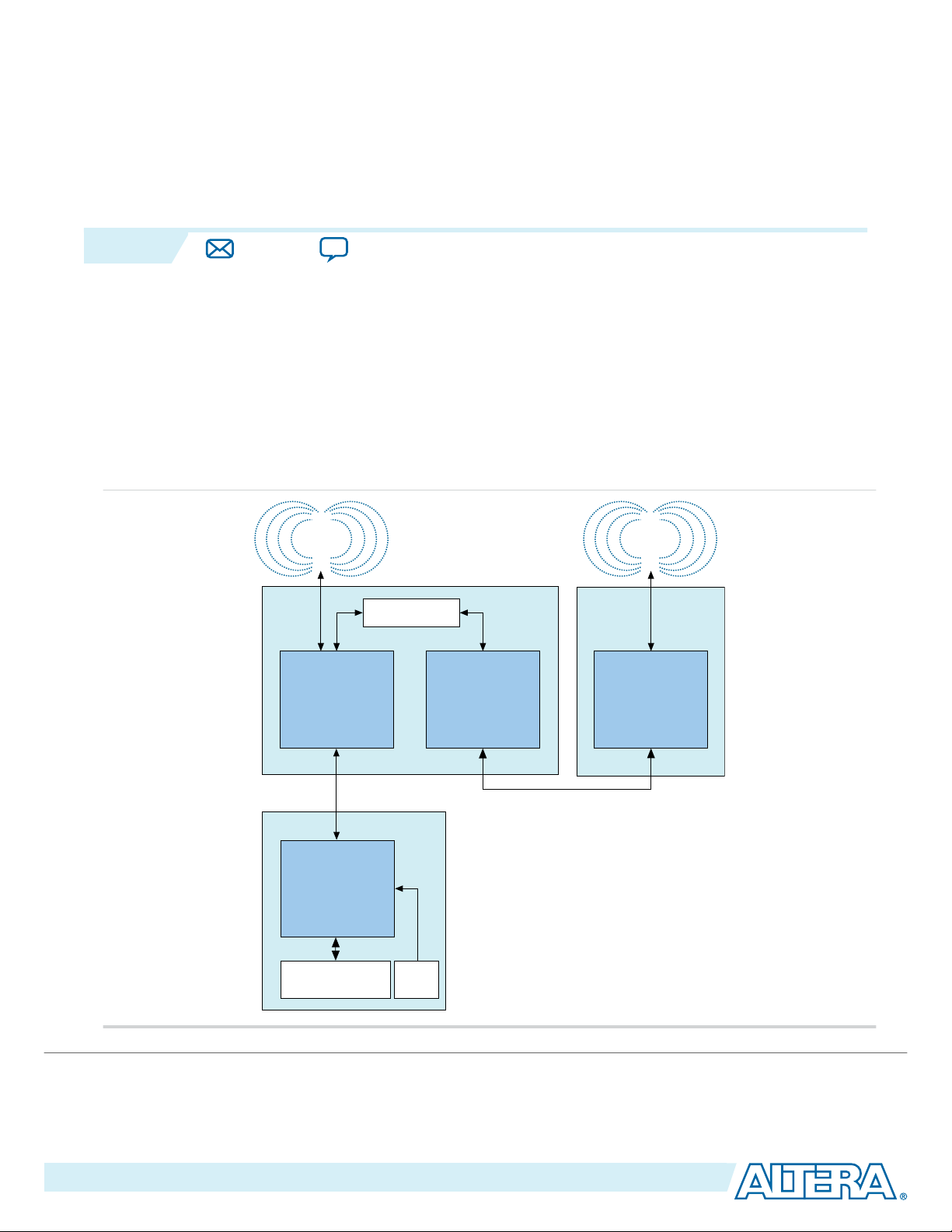
Figure 1-1: Typical CPRI Application on Altera Devices
Example system implementation with a two-hop daisy chain. Optical links between devices support high
performance.
©
2015 Altera Corporation. All rights reserved. ALTERA, ARRIA, CYCLONE, ENPIRION, MAX, MEGACORE, NIOS, QUARTUS and STRATIX words and logos are
trademarks of Altera Corporation and registered in the U.S. Patent and Trademark Office and in other countries. All other words and logos identified as
trademarks or service marks are the property of their respective holders as described at www.altera.com/common/legal.html. Altera warrants performance
of its semiconductor products to current specifications in accordance with Altera's standard warranty, but reserves the right to make changes to any
products and services at any time without notice. Altera assumes no responsibility or liability arising out of the application or use of any information,
product, or service described herein except as expressly agreed to in writing by Altera. Altera customers are advised to obtain the latest version of device
specifications before relying on any published information and before placing orders for products or services.
ISO
9001:2008
Registered
Page 6

1-2
CPRI v6.0 IP Core Supported Features
CPRI v6.0 IP Core Supported Features
The CPRI v6.0 IP core offers the following features:
• Compliant with the Common Public Radio Interface (CPRI) Specification V6.0 (2013-08-30) Interface
Specification available on the CPRI Industry Initiative website (www.cpri.info).
• Supports radio equipment controller (REC) and radio equipment (RE) module configurations.
• Supports the following CPRI link features:
• Configurable CPRI communication line bit rate (to 0.6144, 1.2288, 2.4576, 3.0720, 4.9152, 6.144,
9.8304, or 10.1376 Gbps) using Altera on-chip high-speed transceivers.
• CPRI line bit rate auto-rate negotiation support.
• Configurable and run-time programmable operation mode: CPRI link master or CPRI link slave.
• Optional scrambling and descrambling at 4.9152, 6.1440, 9.8304, and 10.1376 Gbps.
• Transmitter (Tx) and receiver (Rx) delay measurement and calibration.
• Optional L1 link status and alarm (Z.130.0) control and status monitoring.
• Access to all Vendor Specific data.
• Diagnostic parallel reverse loopback paths.
• Diagnostic serial and parallel forward loopback paths.
• Diagnostic stand-alone slave testing mode.
• Includes the following interfaces:
UG-01156
2014.08.18
• Register access interface to external or on-chip processor, using the Altera Avalon® Memory-
Mapped (Avalon-MM) interconnect specification.
• Optional auxiliary (AUX) interface for full access to raw CPRI frame. Provides direct access to full
radioframe, synchronizes the frame position with timing references, and enables routing applica‐
tion support from slave to master ports to implement daisy-chain topologies.
• Optional IEEE 802.3 100BASE-X compliant 100Mbps MII for Ethernet frame access.
• Optional direct I/Q access interface enables integration of all user-defined air standard I/Q
mapping schemes.
• Optional vendor specific data access interfaces provide direct access to Vendor Specific (VS),
Control AxC (Ctrl_AxC), and Real-time Vendor Specific (RTVS) subchannels.
• Optional HDLC serial interface provides direct access to slow control and management subchan‐
nels.
• Optional L1 inband interface provides direct access to Z.130.0 link status and alarm control word.
Related Information
CPRI Industry Initiative website
For a detailed specification of the CPRI protocol refer to the CPRI Specification V6.0 (2013-08-30)
Interface Specification available on the CPRI Industry Initiative website.
Altera Corporation
About the CPRI v6.0 IP Core
Send Feedback
Page 7

UG-01156
2014.08.18
CPRI v6.0 IP Core Device Family and Speed Grade Support
CPRI v6.0 IP Core Device Family and Speed Grade Support
The following sections list the device family and device speed grade support offered by the CPRI v6.0 IP
core:
Device Family Support
Table 1-1: Altera IP Core Device Support Levels
Device Support Level Definition
Preliminary Altera has verified the IP core with preliminary
timing models for this device family. The IP core
meets all functional requirements, but might still be
undergoing timing analysis for the device family. It
can be used in production designs with caution.
Final Altera has verified the IP core with final timing
models for this device family. The IP core meets all
functional and timing requirements for the device
family and can be used in production designs.
1-3
Table 1-2: CPRI v6.0 IP Core Device Family Support
Shows the level of support offered by the CPRI v6.0 IP core for each Altera device family.
Device Family Support
Arria V GZ Default support level provided in Quartus II
software v14.0. Refer to the What's New in Altera IP
page of the Altera website.
Stratix V (GX and GT) Default support level provided in Quartus II
software v14.0. Refer to the What's New in Altera IP
page of the Altera website.
Arria 10 (GX and GT) Default support level provided in Quartus II
software v14.0 Arria 10 Edition. Refer to the What's
New in Altera IP page of the Altera website.
Other device families No support
Related Information
CPRI v6.0 IP Core Performance: Device Speed Grade Support on page 1-4
What's New in Altera IP
About the CPRI v6.0 IP Core
Send Feedback
Altera Corporation
Page 8

1-4
CPRI v6.0 IP Core Performance: Device Speed Grade Support
CPRI v6.0 IP Core Performance: Device Speed Grade Support
Table 1-3: Slowest Supported Device Speed Grades
Lower speed grade numbers correspond to faster devices. The entry -x indicates that both the industrial speed
grade Ix and the commercial speed grade Cx are supported for this device family and CPRI line bit rate.
CPRI Line Bit Rate (Gbps) Arria V GZ Stratix V GX Stratix V GT
0.6144
1.2288
2.4576
-4 -4 -3
3.072
4.9152
6.1440
UG-01156
2014.08.18
9.8304 -3
10.1376
(1)
IP Core Verification
To ensure functional correctness of the CPRI v6.0 IP core, Altera performs extensive validation through
both simulation and hardware testing. Before releasing a version of the CPRI v6.0 IP core, Altera runs
comprehensive regression tests in the associated version of the Quartus® II software.
Related Information
• Knowledge Base Errata for CPRI v6.0 IP core
Exceptions to functional correctness are documented in the CPRI v6.0 IP core errata.
Resource Utilization for CPRI v6.0 IP Cores
Resource utilization changes depending on the parameter settings you specify in the CPRI v6.0 parameter
editor. For example, with every additional interface you enable, the IP core requires additional resources
to implement the module that supports that interface.
-2 -2
(1)
This CPRI line bit rate is not supported for this device family.
Altera Corporation
About the CPRI v6.0 IP Core
Send Feedback
Page 9

UG-01156
2014.08.18
Resource Utilization for CPRI v6.0 IP Cores
Table 1-4: IP Core FPGA Resource Utilization
Lists the resources and expected performance for selected variations of the CPRI v6.0 IP core in an Arria 10
(10AX115R2F40I2LG), Stratix V (5SGSMD4E2H29C2), or Arria V GZ (5AGZME5K2F40C3) device. All
variations are in Master Operation mode and have a Receiver FIFO depth value of 6.
• Minimum IP core variation: includes no direct interfaces and no L2 interface, supports no loopback mode and
no debug features.
• Maximum IP core variation: includes all direct interfaces and the L2 Ethernet interface, supports all loopback
modes and debug features, has an L2 Ethernet buffer depth parameter value of 7, and an Auxiliary latency
cycle(s) value of 0.
These results were obtained using the Quartus II v14.0 and Quartus II v14.0 Arria 10 Edition software
• The numbers of ALMs and logic registers are rounded up to the nearest 100.
• The numbers of ALMs, before rounding, are the ALMs needed numbers from the Quartus II Fitter Report.
1-5
Arria 10 10.3176 Gbps
Variation
ALMs Logic Registers M20K Blocks
Minimum 600 1200 4
Maximum 2900 3700 16
Stratix V 10.3176 Gbps
Variation
ALMs Logic Registers M20K Blocks
Minimum 700 1300 4
Maximum 3300 4100 18
Arria V GZ 9.8 Gbps
Variation
ALMs Logic Registers M20K Blocks
Minimum 800 1300 2
Maximum 2900 3800 13
Related Information
Fitter Resources Reports in the Quartus II Help
Information about Quartus II resource utilization reporting, including ALMs needed.
About the CPRI v6.0 IP Core
Send Feedback
Altera Corporation
Page 10

1-6
Release Information
Release Information
Table 1-5: CPRI v6.0 IP Core Current Release Information
Item Description
UG-01156
2014.08.18
Compatible
14.0 14.0 Arria 10 Edition
Quartus II
Software
Version
Release Date June 2014 August 2014
Ordering
IP-CPRI-V6
Codes
Product ID 0129
Vendor ID 6AF7
Installation and Licensing Features
The CPRI v6.0 IP core provides OpenCore Plus support.
The following sections describe OpenCore Plus support:
OpenCore Plus Evaluation on page 1-6
OpenCore Plus Time-Out Behavior on page 1-7
Related Information
Release Information on page 1-6
OpenCore Plus Evaluation
Altera's OpenCore Plus evaluation feature is available for the CPRI v6.0 IP core. With the OpenCore Plus
evaluation feature, you can perform the following actions:
• Simulate the behavior of a MegaCore function or megafunction in your system.
• Verify the functionality of your design, as well as evaluate its size and speed quickly and easily.
• Generate time-limited device programming files for designs that include MegaCore functions.
• Program a device and verify your design in hardware.
You need to purchase a license for the megafunction only when you are completely satisfied with its
functionality and performance, and want to take your design to production.
Related Information
AN 320: OpenCore Plus Evaluation of Megafunctions
Information about the OpenCore Plus feature.
Altera Corporation
About the CPRI v6.0 IP Core
Send Feedback
Page 11

UG-01156
2014.08.18
OpenCore Plus Time-Out Behavior
OpenCore Plus hardware evaluation can support the following two modes of operation:
• Untethered—the design runs for a limited time.
• Tethered—requires a connection between your board and the host computer. If tethered mode is
supported by all MegaCore functions in a design, the device can operate for a longer time or
indefinitely.
All MegaCore functions in a device time-out simultaneously when the most restrictive evaluation time is
reached. If a design contains more than one MegaCore function, a specific IP core's time-out behavior
may be masked by the time-out behavior of the other IP cores.
Note: For MegaCore functions, the untethered time-out is 1 hour; the tethered time-out value is
indefinite.
Your design stops working after the hardware evaluation time expires.
Related Information
AN 320: OpenCore Plus Evaluation of Megafunctions
Information about the OpenCore Plus feature.
OpenCore Plus Time-Out Behavior
1-7
About the CPRI v6.0 IP Core
Send Feedback
Altera Corporation
Page 12

2014.08.18
www.altera.com
101 Innovation Drive, San Jose, CA 95134
Getting Started with the CPRI v6.0 IP Core
2
UG-01156
Subscribe
Send Feedback
Explains how to install, parameterize, and simulate the Altera CPRI v6.0 IP core.
Installation and Licensing on page 2-2
The CPRI v6.0 IP core is an extended IP core which is not included with the Quartus II release. This
section provides a general overview of the Altera extended IP core installation process to help you quickly
get started with any Altera extended IP core.
Specifying IP Core Parameters and Options on page 2-2
After you install and integrate the extended IP core in the ACDS release, the CPRI v6.0 IP core supports
the standard customization and generation process. This IP core does not generate a testbench or example
design simultaneously with generation of the IP core. Instead, you must use the Example Design button in
the CPRI v6.0 parameter editor to generate the testbench. This IP core is not supported in Qsys.
Files Generated for Altera IP Cores on page 2-3
The Quartus software generates the following IP core output file structure.
CPRI v6.0 IP Core Parameters on page 2-7
The CPRI v6.0 parameter editor provides the parameters you can set to configure the CPRI v6.0 IP core
and simulation testbench.
Integrating Your IP Core in Your Design: Required External Blocks on page 2-11
You must connect your CPRI v6.0 IP core to some additional required design components. Your design
can compile without some of these connections and logical blocks, but it will not function correctly in
hardware unless all of them are present and connected in your design.
Simulating Altera IP Cores on page 2-16
The Quartus II software supports RTL- and gate-level design simulation of Altera IP cores in supported
EDA simulators. Simulation involves setting up your simulator working environment, compiling
simulation model libraries, and running your simulation.
Understanding the Testbench on page 2-17
Altera provides a demonstration testbench with the CPRI v6.0 IP core.
Running the Testbench on page 2-17
To run the Altera CPRI v6.0 IP core demonstration testbench, follow these steps.
Related Information
Managing Quartus II Projects
Refer to the "Integrating IP Cores" section of this Quartus II Handbook chapter for more information
about generating an Altera IP core and integrating it in your Quartus II project.
©
2015 Altera Corporation. All rights reserved. ALTERA, ARRIA, CYCLONE, ENPIRION, MAX, MEGACORE, NIOS, QUARTUS and STRATIX words and logos are
trademarks of Altera Corporation and registered in the U.S. Patent and Trademark Office and in other countries. All other words and logos identified as
trademarks or service marks are the property of their respective holders as described at www.altera.com/common/legal.html. Altera warrants performance
of its semiconductor products to current specifications in accordance with Altera's standard warranty, but reserves the right to make changes to any
products and services at any time without notice. Altera assumes no responsibility or liability arising out of the application or use of any information,
product, or service described herein except as expressly agreed to in writing by Altera. Altera customers are advised to obtain the latest version of device
specifications before relying on any published information and before placing orders for products or services.
ISO
9001:2008
Registered
Page 13

<path>
Quartus II installation directory
ip
Contains the Altera IP Library and third-party IP cores
altera_cloud
Contains the Altera extended IP cores that you install
cpri_ii
Contains the CPRI v6.0 IP core files
2-2
Installation and Licensing
Installation and Licensing
The CPRI v6.0 IP core is an extended IP core which is not included with the Quartus II release. This
section provides a general overview of the Altera extended IP core installation process to help you quickly
get started with any Altera extended IP core.
The Altera extended IP cores are available from the Altera Self-Service Licensing Center (SSLC). Refer to
Related Information below for the correct link for this IP core.
Figure 2-1: IP Core Directory Structure
Directory structure after you install the CPRI v6.0 IP core. The default installation directory <path> on
Windows is C:\altera\< version number >; on Linux it is /opt/altera< version number >.
UG-01156
2014.08.18
Related Information
• Altera website
• Altera Licensing website
• Altera Self-Service Licensing Center
After you purchase the CPRI v6.0 IP core, the IP core is available for download from the SSLC page in
your myAltera account. Altera requires that you create a myAltera account if you do not have one
already, and log in to access the SSLC. On the SSLC page, click Run for this IP core. The SSLC provides
an installation dialog box to guide your installation of the IP core.
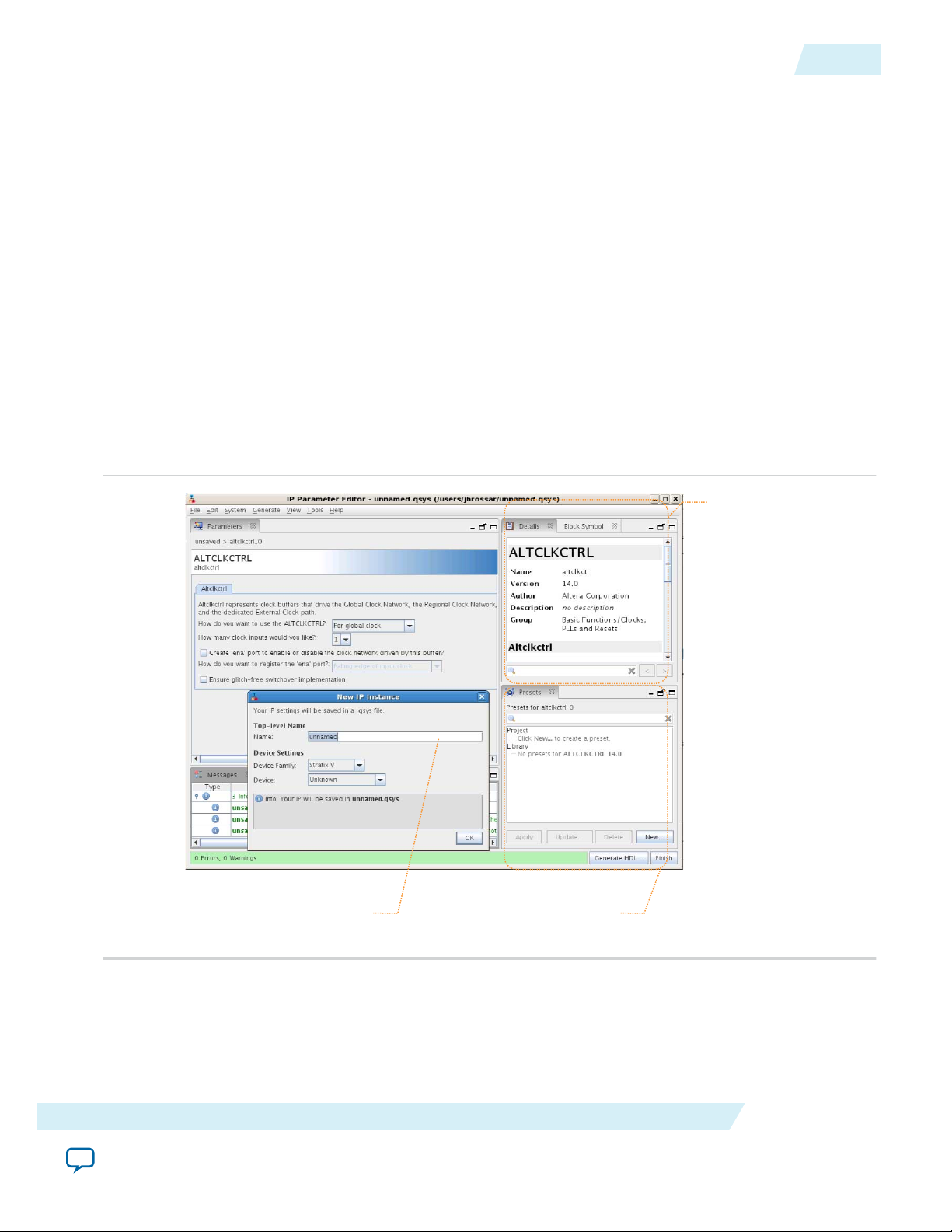
Specifying IP Core Parameters and Options
The parameter editor GUI allows you to quickly configure your custom IP variation. Use the following
steps to specify IP core options and parameters in the Quartus II software. Refer to Specifying IP Core
Parameters and Options (Legacy Parameter Editors) for configuration of IP cores using the legacy
parameter editor.
1. In the IP Catalog (Tools > IP Catalog), locate and double-click the name of the IP core to customize.
The parameter editor appears.
2. Specify a top-level name for your custom IP variation. The parameter editor saves the IP variation
settings in a file named <your_ip>.qsys. Click OK.
Altera Corporation
3. Specify the parameters and options for your IP variation in the parameter editor, including one or
more of the following. Refer to your IP core user guide for information about specific IP core
parameters.
Getting Started with the CPRI v6.0 IP Core
Send Feedback
Page 14
View IP port
and parameter
details
Apply preset parameters for
specific applications
Specify your IP variation name
and target device
UG-01156
2014.08.18
Files Generated for Altera IP Cores
• Optionally select preset parameter values if provided for your IP core. Presets specify initial
parameter values for specific applications.
• Specify parameters defining the IP core functionality, port configurations, and device-specific
features.
• Specify options for processing the IP core files in other EDA tools.
4. Click Generate HDL, the Generation dialog box appears.
5. Specify output file generation options, and then click Generate. The IP variation files generate
according to your specifications.
6. To generate a simulation testbench, click Generate > Generate Testbench System.
7. To generate an HDL instantiation template that you can copy and paste into your text editor, click
Generate > HDL Example.
8. Click Finish. The parameter editor adds the top-level .qsys file to the current project automatically. If
you are prompted to manually add the .qsys file to the project, click Project > Add/Remove Files in
Project to add the file.
9. After generating and instantiating your IP variation, make appropriate pin assignments to connect
ports.
Figure 2-2: IP Parameter Editor
2-3
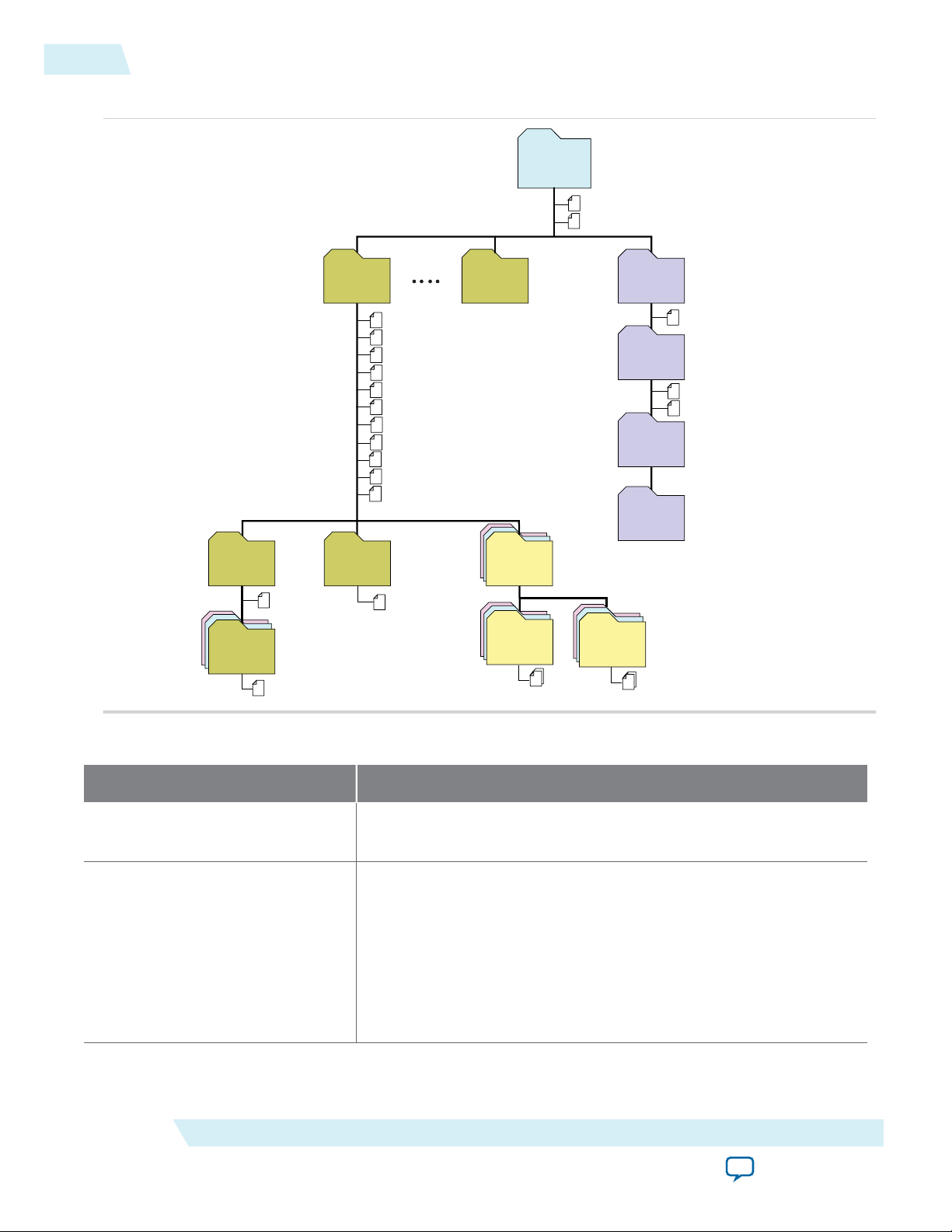
Files Generated for Altera IP Cores
The Quartus software generates the following IP core output file structure.
Getting Started with the CPRI v6.0 IP Core
Send Feedback
Altera Corporation
Page 15
<your_testbench>_tb.csv
<your_testbench>_tb.spd
<your_ip>.cmp - VHDL component declaration file
<your_ip>.ppf - XML I/O pin information file
<your_ip>.qip - Lists IP synthesis files
<your_ip>.sip - Lists files for simulation
<your_ip>.v or .vhd
Top-level IP synthesis file
<your_ip>.v or .vhd
Top-level simulation file
<simulator_setup_scripts>
<your_ip>.qsys - System or IP integration file
<your_ip>_bb.v - Verilog HDL black box EDA synthesis file
<your_ip>_inst.v or .vhd - Sample instantiation template
<your_ip>_generation.rpt - IP generation report
<your_ip>.debuginfo - Contains post-generation information
<your_ip>.html - Connection and memory map data
<your_ip>.bsf - Block symbol schematic
<your_ip>.spd - Combines individual simulation scripts
<your_ip>_tb.qsys
Testbench system file
<your_ip>.sopcinfo - Software tool-chain integration file
<project directory>
<EDA tool setup
scripts>
<your_ip>
IP variation files
<testbench>_tb
testbench system
sim
Simulation files
synth
IP synthesis files
sim
simulation files
<EDA tool name>
Simulator scripts
<testbench>_tb
<ip subcores> n
Subcore libraries
sim
Subcore
Simulation files
synth
Subcore
synthesis files
<HDL files>
<HDL files>
<your_ip> n
IP variation files
testbench files
2-4
Files Generated for Altera IP Cores
Figure 2-3: IP Core Generated Files
UG-01156
2014.08.18
Altera Corporation
Table 2-1: IP Core Generated Files
File Name Description
<my_ip>.qsys
<system>.sopcinfo Describes the connections and IP component parameterizations in
The Qsys system or top-level IP variation file. <my_ip> is the name
that you give your IP variation.
your Qsys system. You can parse its contents to get requirements
when you develop software drivers for IP components.
Downstream tools such as the Nios II tool chain use this file.
The .sopcinfo file and the system.h file generated for the Nios II tool
chain include address map information for each slave relative to each
master that accesses the slave. Different masters may have a different
address map to access a particular slave component.
Getting Started with the CPRI v6.0 IP Core
Send Feedback
Page 16

UG-01156
2014.08.18
Files Generated for Altera IP Cores
File Name Description
<my_ip>.cmp The VHDL Component Declaration (.cmp) file is a text file that
contains local generic and port definitions that you can use in VHDL
design files.
2-5
<my_ip>.html
A report that contains connection information, a memory map
showing the address of each slave with respect to each master to
which it is connected, and parameter assignments.
<my_ip>_generation.rpt IP or Qsys generation log file. A summary of the messages during IP
generation.
<my_ip>.debuginfo Contains post-generation information. Used to pass System Console
and Bus Analyzer Toolkit information about the Qsys interconnect.
The Bus Analysis Toolkit uses this file to identify debug components
in the Qsys interconnect.
<my_ip>.qip
Contains all the required information about the IP component to
integrate and compile the IP component in the Quartus software.
<my_ip>.csv Contains information about the upgrade status of the IP component.
<my_ip>.bsf A Block Symbol File (.bsf) representation of the IP variation for use
in Quartus Block Diagram Files (.bdf).
<my_ip>.spd
Required input file for ip-make-simscript to generate simulation
scripts for supported simulators. The .spd file contains a list of files
generated for simulation, along with information about memories
that you can initialize.
<my_ip>.ppf The Pin Planner File (.ppf) stores the port and node assignments for
IP components created for use with the Pin Planner.
<my_ip>_bb.v You can use the Verilog black-box (_bb.v) file as an empty module
declaration for use as a black box.
<my_ip>.sip Contains information required for NativeLink simulation of IP
components. You must add the .sip file to your Quartus project.
<my_ip>_inst.v or _inst.vhd HDL example instantiation template. You can copy and paste the
contents of this file into your HDL file to instantiate the IP variation.
<my_ip>.regmap If IP contains register information, .regmap file generates.
The .regmap file describes the register map information of master
and slave interfaces. This file complements the .sopcinfo file by
providing more detailed register information about the system. This
enables register display views and user customizable statistics in the
System Console.
Getting Started with the CPRI v6.0 IP Core
Send Feedback
Altera Corporation
Page 17

2-6
Files Generated for Altera IP Cores
File Name Description
UG-01156
2014.08.18
<my_ip>.svd
<my_ip>.v
or
<my_ip>.vhd
mentor/
aldec/
/synopsys/vcs
/synopsys/vcsmx
Allows HPS System Debug tools to view the register maps of
peripherals connected to HPS within a Qsys system.
During synthesis, the .svd files for slave interfaces visible to System
Console masters are stored in the .sof file in the debug section.
System Console reads this section, which Qsys can query for register
map information. For system slaves, Qsys can access the registers by
name.
HDL files that instantiate each submodule or child IP core for
synthesis or simulation.
Contains a ModelSim® script msim_setup.tcl to set up and run a
simulation.
Contains a Riviera-PRO script rivierapro_setup.tcl to setup and run a
simulation.
Contains a shell script vcs_setup.sh to set up and run a VCS
®
simulation.
Contains a shell script vcsmx_setup.sh and synopsys_ sim.setup file to
set up and run a VCS MX® simulation.
/cadence
Contains a shell script ncsim_setup.sh and other setup files to set up
and run an NCSIM simulation.
/submodules Contains HDL files for the IP core submodule.
<child IP cores>/ For each generated child IP core directory, Qsys generates /synth and /
sim sub-directories.
Altera Corporation
Getting Started with the CPRI v6.0 IP Core
Send Feedback
Page 18

UG-01156
2014.08.18
CPRI v6.0 IP Core Parameters
CPRI v6.0 IP Core Parameters
The CPRI v6.0 parameter editor provides the parameters you can set to configure the CPRI v6.0 IP core
and simulation testbench.
Table 2-2: General CPRI v6.0 IP Core Parameters
Describes the general parameters for customizing the CPRI v6.0 IP core. These parameters appear on the General
tab in the CPRI v6.0 parameter editor.
2-7
Parameter Range Default
Bit rate (Mbits/s) • 614.4
• 1228.8
• 2457.6
• 3072.0
• 4915.2
• 6144.0
• 9830.4
• 10137.6
Operation mode • Master
• Slave
Supported receiver
CDR frequency
Per drop-down
menu
(MHz)
Parameter Description
Setting
614.4 Selects the CPRI line bit rate.
Arria V GZ devices support all line bit rates except
10.1376 Gbps. All other supported devices support
all CPRI line bit rates.
Master
Specifies whether the CPRI v6.0 IP core is
configured as a CPRI link master or a CPRI link
slave.
The value of this parameter determines the initial
and reset operation mode of the CPRI v6.0 IP core.
You can modify the IP core operation mode
dynamically by modifying the value of the
operation_mode field of the L1_CONFIG register.
307.2
Specifies the incoming reference clock frequency
for the receiver CDR PLL, in MHz.
You must drive the input clock xcvr_cdr_refclk
at the frequency you specify for this parameter.
Getting Started with the CPRI v6.0 IP Core
Send Feedback
Altera Corporation
Page 19

2-8
CPRI v6.0 IP Core Parameters
UG-01156
2014.08.18
Parameter Range Default
Receiver FIFO depth
Enable auto-rate
negotiation
4, 5, 6, 7, or 8 6
• On
• Off
Setting
Off
Parameter Description
The value you specify for this parameter is log2 of
the IP core Layer 1 Rx buffer depth.The IP core
supports a maximum Layer 1 RX buffer depth of
256.
The default depth of the buffer is 64, specified by
the parameter default value of 6. For most systems,
the default buffer depth is adequate to handle
dispersion, jitter, and drift that can occur on the
link while the system is running. However, the
parameter is available for cases in which additional
depth is required.
The user guide refers to this parameter value as
RX_BUF_DEPTH.
Turn on the Enable auto-rate negotiation
parameter to specify that your CPRI v6.0 IP core
supports auto-rate negotiation.
This parameter is available when you specify a
CPRI line bit rate (value for the Bit rate
parameter) that is greater than 614.4 Mbps.
Enable auto-rate
negotiation down to
614.4 Mbps
• On
• Off
Off
Turn on this parameter to specify that your autorate negotiation enabled CPRI v6.0 IP core can
support auto-rate negotiation all the way down to
the CPRI line bit rate of 0.6144 Gbps.
This parameter is available when you turn on
Enable auto-rate negotiation.
Table 2-3: CPRI v6.0 IP Core Interface Feature Parameters
Describes the parameters for customizing the CPRI v6.0 IP core Layer 1 and Layer 2 interfaces and testing
features. These parameters appear on the Interfaces tab in the CPRI v6.0 parameter editor.
Parameter Range Default
Setting
Parameter Description
L1 Features
Supported CPU
interface standard
Currently, only the AvalonMM CPU interface is
available in the CPRI v6.0 IP
Selects the interface specification that describes
the behavior of the CPRI v6.0 IP core register
access interface.
core.
Altera Corporation
Getting Started with the CPRI v6.0 IP Core
Send Feedback
Page 20

UG-01156
2014.08.18
CPRI v6.0 IP Core Parameters
2-9
Parameter Range Default
Auxiliary latency
0 to 9 0
cycle(s)
Parameter Description
Setting
Specifies the additional write latency on the AUX
TX interface and other direct TX interfaces to the
CPRI v6.0 IP core. The write latency is the
number of cpri_clkout cycles from when the
aux_tx_seq output signal has the value of 0 to
when user logic writes data to the AUX TX
interface. For other direct interfaces, the IP core
notifies user logic when it is ready for input and
the user does not need to monitor the aux_tx_
seq signal.
When Auxiliary latency cycle(s) has the value of
zero, the write latency on the direct TX interfaces
is one cpri_clkout cycle. When Auxiliary
latency cycle(s) has the value of N, the write
latency is (1+N) cpri_clkout cycles.
Set this parameter to a value that provides user
logic with sufficient advance notice of the
position in the CPRI frame. The processing time
that user logic requires after determining the
current position in the CPRI frame is implemen‐
tation specific.
Enable auxiliary
interface
Enable all control
word access
Enable direct IQ
mapping interface
• On
• Off
• On
• Off
• On
• Off
Off
Off
Off
This parameter is available if you turn on at least
one direct interface in your CPRI v6.0 IP core
variation.
Turn on this parameter to include the AUX
interface in your CPRI v6.0 IP core. The AUX
interface provides full access to the raw CPRI
frame.
Turn on this parameter to enable access to all
control words in a hyperframe using the CPRI
v6.0 CTRL_INDEX, TX_CTRL, and RX_CTRL
registers.
Use this option with caution. During transmis‐
sion, this feature has higher priority than the MII,
the HDLC serial interface, the L1 control and
status interface, and the generation of special
symbols (K28.5, D16.2, /S/, /T/) , and can
overwrite standard control words in the
hyperframe.
Turn on this parameter to include a dedicated
interface to access the raw I/Q data bytes in the
CPRI frame.
Getting Started with the CPRI v6.0 IP Core
Send Feedback
Altera Corporation
Page 21

2-10
CPRI v6.0 IP Core Parameters
UG-01156
2014.08.18
Parameter Range Default
Enable direct ctrl_axc
access interface
Enable direct vendor
specific access
• On
• Off
• On
• Off
interface
Enable start-up
sequence state
• On
• Off
machine
Enable L1 inband
protocol negotiator
• On
• Off
Setting
Off
Off
Off
Off
Parameter Description
Turn on this parameter to include a dedicated
interface to access the Ctrl_AxC subchannels in
the CPRI frame.
Turn on this parameter to include a dedicated
interface to access the VS subchannels in the
CPRI frame.
Turn on this parameter to include a start-up
sequence state machine in the CPRI v6.0 IP core.
Turn on this parameter to include a negotiator
block that performs auto-negotiation of L1
inband protocol version (communicated in CPRI
frame position Z.2.0) and L2 C&M rates
(communicated in CPRI frame positions Z.66.0
and Z.194.0).
This parameter is available when you turn on
Enable start-up sequence state machine.
Enable real-time
vendor specific
interface (R-16A)
Enable Z.130.0 access
interface
L2 Features
Enable direct HDLC
serial interface
Enable IEEE 802.3
100BASE-X 100Mbps
MII
• On
• Off
• On
• Off
• On
• Off
• On
• Off
Off
Off
Off
Off
Turn on this parameter to include a dedicated
interface to access the RTVS subchannel in the
CPRI frame.
This parameter is available when you specify a
CPRI line bit rate of 10137.6 Mbps.
Turn on this parameter to include a dedicated L1
control and status interface to communicate the
contents of the CPRI frame Z.130.0 word, which
includes alarms and reset signals.
Turn on this parameter to include a dedicated
interface to communicate the contents of the slow
C&M subchannels.
For full HDLC communication, you must
connect a user-defined HDLC module to this
interface.
Turn on this parameter to include an MII port to
communicate with the fast C&M (Ethernet) CPRI
subchannel.
Altera Corporation
For full Ethernet communication, you must
connect a user-defined Ethernet MAC to this
interface.
Getting Started with the CPRI v6.0 IP Core
Send Feedback
Page 22

UG-01156
2014.08.18
Integrating Your IP Core in Your Design: Required External Blocks
2-11
Parameter Range Default
L2 Ethernet PCS Tx/
7, 8, 9, 10 7
Rx FIFO depth
Debug Features
Enable debug
interface
Enable transceiver
PMA forward
• On
• Off
• On
• Off
loopback path (Tx to
Rx)
Setting
Off
Off
Parameter Description
The value you specify for this parameter is log2 of
the IP core Layer 2 Ethernet PCS Rx buffer depth
and Tx buffer depth. The IP core supports a
maximum Layer 2 Ethernet PCS buffer depth of
1024.
This parameter is available when you turn on
Enable IEEE 802.3 100BASE-X 100Mbps MII.
Turn on this parameter to include dedicated
transceiver status and L1 Rx status interfaces to
support debug.
Turn on this parameter to enable transceiver
PMA serial forward loopback. To turn on
transceiver PMA serial forward loopback, you
must also write the value of 2'b01 to the loop_
forward field of the LOOPBACK register at offset
0x44.
Enable forward
loopback path (Tx to
Rx)
• On
• Off
Off
Turn on this parameter to enable other internal
parallel forward loopback paths. To turn on
internal parallel forward loopback, you must also
write a non-zero value to the loop_forward field
of the LOOPBACK register at offset 0x44.
Enable reverse
loopback path (Rx to
Tx)
• On
• Off
Off
Turn on this parameter to enable internal parallel
reverse loopback. To turn on reverse loopback,
you must also write a non-zero value to the loop_
reversed field of the LOOPBACK register at offset
0x44, to specify the parts of the CPRI frame that
are sent on the loopback path.
Related Information
LOOPBACK Register on page 5-14
Integrating Your IP Core in Your Design: Required External Blocks
You must connect your CPRI v6.0 IP core to some additional required design components. Your design
can compile without some of these connections and logical blocks, but it will not function correctly in
hardware unless all of them are present and connected in your design.
Getting Started with the CPRI v6.0 IP Core
Send Feedback
Altera Corporation
Page 23
Reset Controller
Reset Controller
TX
PLL
Transmitter
(Native PHY)
Receiver
(Native PHY)
User-Defined
Reference Clock
xcvr_ext_pll_clk
xcvr_tx_analogreset
xcvr_tx_digitalreset
xcvr_tx_cal_busy
xcvr_rx_analogreset
xcvr_rx_digitalreset
xcvr_rx_is_lockedtodata
xcvr_rx_cal_busy
xcvr_cdr_refclk
reset_tx
reset_rx
pll_locked
CPRI v6.0 IP Core
xcvr_reset_tx_ready
xcvr_reset_rx_ready
2-12
Adding the Clean-Up PLL
The CPRI v6.0 IP core requires that you define, instantiate, and connect the following additional software
and hardware modules for all CPRI v6.0 IP core variations:
• An external PLL IP core to configure the transceiver TX PLL. Although the hardware this IP core
configures is physically part of the device transceiver, you must instantiate it in software separately
from the CPRI v6.0 IP core. In Arria 10 devices, this Altera requirement supports the configuration of
multiple Altera IP cores using the same transceiver block in the device.
• One or more external reset controllers to coordinate the reset sequence for the CPRI v6.0 IP core in
your design.
In addition, CPRI link slave modules require an external clean-up PLL and Arria V GZ and Stratix V
variations require an external transceiver reconfiguration controller.
Figure 2-4: Required External Blocks
An example showing how you could connect required components to a single CPRI v6.0 IP core.
UG-01156
2014.08.18
Altera Corporation
Related Information
Adding the External Reset Controller on page 2-14
Adding the Clean-Up PLL
If your CPRI v6.0 IP core is an RE slave, you must connect it to an external clean-up PLL to clean up any
jitter that occurs in the CDR output clock before sending it to the external TX PLL.
The clean-up PLL performs the clock synchronization necessary to address the CPRI v6.0 Specification
requirements R-17, R-18, and R-18A, which address jitter and frequency accuracy in the RE core clock for
radio transmisstion.
Getting Started with the CPRI v6.0 IP Core
Send Feedback
Page 24

UG-01156
2014.08.18
Drive the clean-up PLL with the CPRI v6.0 IP core xcvr_recovered_clk output clock, and connect the
cleaned up output to the external TX PLL input reference clock port.
Related Information
CPRI v6.0 IP Core Clocking Structure on page 3-3
Adding the External TX PLL
The CPRI v6.0 IP core requires that you generate and connect an external TX PLL IP core. The
transceiver PLL IP core configures the TX PLL in the transceiver in hardware, but you must generate the
transceiver PLL IP core separately from the CPRI v6.0 IP core in software. If you do not generate and
connect the transceiver PLL IP core, the CPRI v6.0 IP core does not compile.
You can use the IP Catalog to generate the external PLL IP core that configures a TX PLL on the device. In
the IP Catalog, select an Altera IP core that configures an appropriate PLL on your target device.
In the Stratix V TX PLL parameter editor, you must set the following parameter values:
• Enable PLL reconfiguration: Turn on if you turned on Enable auto-rate negotiation in the CPRI v6.0
parameter editor. Otherwise, turn off.
• Number of TX PLL reference clocks: 1.
• PLL feedback path: Set to internal.
• PLL type: Select a type that supports the CPRI line bit rate you specified in the CPRI v6.0 parameter
editor.
• PLL base data rate: Set to the CPRI line bit rate you specified in the CPRI v6.0 parameter editor.
• Selected reference clock source: Set to 0.
Adding the External TX PLL
2-13
For your Arria 10 design, you can select Arria 10 Transceiver ATX PLL, Arria 10 Transceiver CMU
PLL, or Arria 10 FPLL in the IP Catalog. In the parameter editor for the TX PLL IP core you select, you
must set the following parameter values:
• PLL output frequency to one half the per-lane data rate of the IP core variation. The transceiver
performs dual edge clocking, using both the rising and falling edges of the input clock from the PLL.
Therefore, this PLL output frequency setting drives the transceiver with the correct clock for the
Interlaken lanes.
• PLL reference clock frequency to a frequency at which you can drive the TX PLL input reference
clock. You must drive the external PLL reference clock input signal at the frequency you specify for
this parameter.
Arria 10 devices and the Quartus II software support multiple options for configuring an Arria 10 TX
PLL. Depending on the TX PLL IP core you select and the configuration options you prefer, you have a
wide range of choices in parameterizing the external TX PLL for an Arria 10 variation.
You must connect the external TX PLL signals and the CPRI v6.0 IP core transceiver TX PLL interface
signals according to the following rules:
• Connect the xcvr_ext_pll_clk input signal of the CPRI v6.0 IP core to the pll_clkout or
tx_serial_clk output signal of the external PLL IP core.
• If your CPRI v6.0 IP core is an RE slave, drive the input signal of the external PLL IP core with the
output of the external cleanup PLL.
Getting Started with the CPRI v6.0 IP Core
Send Feedback
Altera Corporation
Page 25

2-14
Adding the External Reset Controller
User logic must provide the connection. Refer to the demonstration testbench for example working user
logic including one correct method to instantiate and connect the external PLL to a single CPRI v6.0 IP
core.
Related Information
Interface to the External PLL on page 3-48
Altera Transceiver PHY IP Core User Guide
Information about how to configure an external PLL for your Arria V GZ or Stratix V design.
Arria 10 Transceiver PHY User Guide
Information about how to configure an external PLL for your own Arria 10 design.
Adding the External Reset Controller
The CPRI v6.0 IP core requires that you provide reset control logic to handle the required reset sequence
for the IP core transceiver on the device. Altera recommends that you generate and connect two Altera
Transceiver PHY Reset Controller IP cores to perform this function, one reset controller for the TX
transceiver and data path and one reset controller for the RX transceiver and data path in the CPRI v6.0
IP core. If you do not implement the device-specific correct reset sequence, the IP core does not function
correctly in hardware.
UG-01156
2014.08.18
You can use the IP Catalog to generate Altera Transceiver PHY Reset Controller IP cores for the device
family that your CPRI v6.0 IP core targets.
Follow the instructions in the Altera Transceiver PHY IP Core User Guide or the Arria 10 Transceiver PHY
User Guide. The CPRI v6.0 IP core configures the Native PHY IP core for the target device family. You
must configure the reset controllers to coordinate reset of the CPRI v6.0 IP core including the Native PHY
IP core, and the external PLL IP core. In the case of Arria V GZ and Stratix V variations, the reset control‐
lers must also coordinate with the transceiver reconfiguration controller.
To configure a TX reset controller, in the Altera Transceiver PHY Reset Controller parameter editor, you
must set the following parameter values:
• Set Input clock frequency to a value in the range of 100–150.
• Turn on Synchronize reset input.
• Turn on Use fast reset for simulation.
• Turn on Enable TX PLL reset control.
• Set pll_powerdown duration to the value of 10.
• Turn on Enable TX channel reset control.
• Leave all other parameters turned off or for the parameters that do not turn on or off, at their default
values.
To configure an RX reset controller, in the Altera Transceiver PHY Reset Controller parameter editor,
you must set the following parameter values:
• Set Input clock frequency to a value in the range of 100–150.
• Turn on Synchronize reset input.
• Turn on Use fast reset for simulation.
• Turn on Enable RX channel reset control.
• Leave all other parameters turned off or for the parameters that do not turn on or off, at their default
Altera Corporation
values.
Getting Started with the CPRI v6.0 IP Core
Send Feedback
Page 26

UG-01156
2014.08.18
Adding the Transceiver Reconfiguration Controller
2-15
You must connect the external reset controller signals and the CPRI v6.0 IP core reset controller interface
signals according to the following rules. Refer to Integrating Your IP Core in Your Design: Required
External Blocks on page 2-11 for an illustration of the connections.
• Connect the tx_digitalreset, tx_analogreset, tx_ready, rx_digitalreset, rx_analogreset,
and rx_ready output signals of the reset controllers to the xcvr_tx_digitalreset,
xcvr_tx_analogreset, xcvr_tx_ready, xcvr_rx_digitalreset, xcvr_rx_analogreset, and
xcvr_rx_readyinput signals of the CPRI v6.0 IPcore, respectively.
• Connect the xcvr_rx_is_lockedtodata output pin of the CPRI v6.0 IP core to the rx_is_lockedto-
data input signal of the RX reset controller.
User logic must provide the connections. Refer to the demonstration testbench for example working user
logic including one correct method to instantiate and connect the external reset controllers.
Related Information
• Interface to the External Reset Controller on page 3-47
• Integrating Your IP Core in Your Design: Required External Blocks on page 2-11
Figure illustrates the required connections.
• Altera Transceiver PHY IP Core User Guide
Information about how to configure the Altera Transceiver PHY Reset Controller for your Arria V GZ
or Stratix V design.
• Arria 10 Transceiver PHY User Guide
Information about how to configure the Altera Transceiver PHY Reset Controller for your Arria 10
design.
Adding the Transceiver Reconfiguration Controller
CPRI v6.0 IP cores that target Arria V GZ and Stratix V devices require an external reconfiguration
controller to compile and to function correctly in hardware. CPRI v6.0 IP cores that target Arria 10
devices include a transceiver reconfiguration controller block and do not require an external reconfigura‐
tion controller.
You can use the IP Catalog to generate the Altera Transceiver Reconfiguration Controller IP core.
When you configure the Altera Transceiver Reconfiguration Controller, you must specify the number of
reconfiguration interfaces. The number of reconfiguration interfaces required for the CPRI v6.0 IP core is
two . You can configure your reconfiguration controller with additional interfaces if your design connects
with multiple transceiver IP cores. You can leave other options at the default settings or modify them for
your preference.
You should connect the reconfig_to_xcvr and reconfig_from_xcvr ports of the CPRI v6.0 IP core to
the corresponding ports of the reconfiguration controller.
You must drive the CPRI v6.0 IP core reconfig_clk input port and the Altera Transceiver Reconfigura‐
tion Controller mgmt_clk_clk input port from the same clock source. Drive both ports at a clock
frequency in the range of 100–150MHz.
Related Information
• Arria V GZ and Stratix V Transceiver Reconfiguration Interface on page 3-46
• Altera Transceiver PHY IP Core User Guide
For more information about the Altera Transceiver Reconfiguration Controller.
Getting Started with the CPRI v6.0 IP Core
Send Feedback
Altera Corporation
Page 27
Post-fit timing
simulation netlist
Post-fit timing
simulation (3)
Post-fit functional
simulation netlist
Post-fit functional
simulation
Analysis & Synthesis
Fitter
(place-and-route)
TimeQuest Timing Analyzer
Device Programmer
Quartus II
Design Flow
Gate-Level Simulation
Post-synthesis
functional
simulation
Post-synthesis functional
simulation netlist
(Optional) Post-fit
timing simulation
RTL Simulation
Design Entry
(HDL, Qsys, DSP Builder)
Altera Simulation
Models
EDA
Netlist
Writer
2-16
Simulating Altera IP Cores
Simulating Altera IP Cores
The Quartus II software supports RTL- and gate-level design simulation of Altera IP cores in supported
EDA simulators. Simulation involves setting up your simulator working environment, compiling
simulation model libraries, and running your simulation.
You can use the functional simulation model and the testbench or example design generated with your IP
core for simulation. The functional simulation model and testbench files are generated in a project
subdirectory. This directory may also include scripts to compile and run the testbench. For a complete list
of models or libraries required to simulate your IP core, refer to the scripts generated with the testbench.
Figure 2-5: Simulation in Quartus II Design Flow
UG-01156
2014.08.18
Altera Corporation
Note: Altera IP supports a variety of simulation models, including simulation-specific IP functional
simulation models and encrypted RTL models, and plain text RTL models. These are all
cycle-accurate models. The models support fast functional simulation of your IP core instance
using industry-standard VHDL or Verilog HDL simulators. For some cores, only the plain text
RTL model is generated, and you can simulate that model. Use the simulation models only for
simulation and not for synthesis or any other purposes. Using these models for synthesis creates a
nonfunctional design.
Related Information
Simulating Altera Designs
Getting Started with the CPRI v6.0 IP Core
Send Feedback
Page 28

UG-01156
2014.08.18
Understanding the Testbench
Altera provides a demonstration testbench with the CPRI v6.0 IP core.
If you click Example Design in the CPRI v6.0 parameter editor, the Quartus II software generates the
demonstration testbench. The parameter editor prompts you for the desired location of the testbench.
The testbench is static and does not necessarily match your IP core variation; you can generate it without
generating an IP core. The testbench scripts generate a DUT that matches the testbench, but you must
manually set the appropriate values for the DUT in the parameter editor before you create the demonstra‐
tion testbench.
The testbench performs the following sequence of actions with the static DUT:
1. Enables transmission on the CPRI link by setting the tx_enable bit (bit [0]) of the CPRI v6.0 IP core
L1_CONFIG register at offset 0x8 (and resetting all other fields of the register)>
2. Configures the DUT at the highest possible HDLC bit rate (for CPRI line bit rate 6.144 Gbps), by
setting the tx_slow_cm_rate field of the CPRI v6.0 CM_CONFIG register at offset 0x1C to the value of
3'b110.
3. Reads the CM_CONFIG regster to confirm settings.
4. After the DUT and the testbench achieve link synchronization, executes the following transactions:
Understanding the Testbench
2-17
a. Performs ten write transactions to the AUX Tx interface and confirms the testbench receives them
on the CPRI link.
b. Performs three write transactions to the VS interface and confirms the testbench receives them
from the DUT on the CPRI link.
c. Performs three write transactions to the Ctrl_AxC interface and confirms the testbench receives
them from the DUT on the CPRI link.
d. Performs 50 HDLC transactions and confirms the testbench receives them from the DUT on the
CPRI link.
e. Performs ten write transactions to the MI interface and confirms the testbench receives them from
the DUT on the CPRI link.
f. Calculates the round-trip delay through the IP core.
Running the Testbench
To run the Altera CPRI v6.0 IP core demonstration testbench, follow these steps.
1. In the Quartus II software IP Catalog, select the CPRI v6.0 IP core and click Add.
2. When prompted, you can specify any output file type (HDL). This setting is relevant only for synthesis
and does not impact simulation of the demonstration testbench.
3. In the CPRI v6.0 parameter editor, set the following parameter values:
Table 2-4: CPRI v6.0 IP Core Variation for Demonstration Testbench
The testbench scripts require that you set these values in the CPRI v6.0 parameter editor before you click Example
Design. The scripts generate the DUT but they require that you provide the parameter values.
Parameter Value
Bit rate (Mbit/s) 6144.0
Getting Started with the CPRI v6.0 IP Core
Send Feedback
Altera Corporation
Page 29

2-18
Running the Testbench
Parameter Value
Operation mode Master
Supported receiver CDR frequency (MHz) 307.2
UG-01156
2014.08.18
Receiver FIFO depth (value shown is log2 of actual
6
depth)
Enable auto-rate negotiation Turn off
Enable auto-rate negotiation down to 614.4Mbps Not available
Supported CPU interface standard AvalonMM
Auxiliary latency cycle(s) 0
Enable auxiliary interface Turn on
Enable all control word access Turn off
Enable direct IQ mapping interface Turn off
Enable direct ctrl_axc access interface Turn on
Enable direct vendor specific access interface Turn on
Enable start-up sequence state machine Turn off
Enable L1 inband protocol negotiator Not available
Enable real-time vendor specific interface (R-16A) Not available
Enable Z.130.0 access interface Turn off
Enable direct HDLC serial interface Turn on
Enable IEEE 802.3 100BASE-X 100Mbps MII Turn on
L2 Ethernet PCS Tx/Rx FIFO depth (value shown is
Turn off
log2 of actual depth)
Enable debug interface Turn off
Enable transceiver PMA forward loopback path (Tx
Turn off
to Rx)
Enable forward loopback path (Tx to Rx) Turn off
Enable reversed loopback path (Rx to Tx) Turn off
4. In the CPRI v6.0 parameter editor, click the Example Design button and specify the desired location
of the testbench.
5. After you generate the demonstration testbench, in the Quartus II software, click View > Utility
Windows > Tcl Console.
6. In the Tcl Console, change directory to your specified testbench directory's ip_sim subdirectory.
7. Type source gen_sim_verilog.tcl or source gen_sim_vhdl.tcl, depending on the language of
the model you wish to simulate. Running this script generates the DUT and testbench files.
8. If you are using a simulator that requires that you open a user interface, open your target simulator.
Altera Corporation
Getting Started with the CPRI v6.0 IP Core
Send Feedback
Page 30

UG-01156
2014.08.18
Running the Testbench
2-19
Note: You must select a simulator that is supported by the Quartus II v14.0 or v14.0 Arria 10 Edition
software, as appropriate.
9. Change directory to your specified testbench directory's testbench/<simulator vendor> subdirectory.
10.Execute the simulation script in the directory.
• In the Mentor Graphics ModelSim simulator, type do run_altera_cpri_v6_tb.tcl
• In the Synopsys VCS-MX simulator, type sh run_altera_cpri_v6_vcsmx_tb.sh
• In the Cadence NCSIM simulator, type sh run_altera_cpri_v6_tb.sh
Getting Started with the CPRI v6.0 IP Core
Send Feedback
Altera Corporation
Page 31

2014.08.18
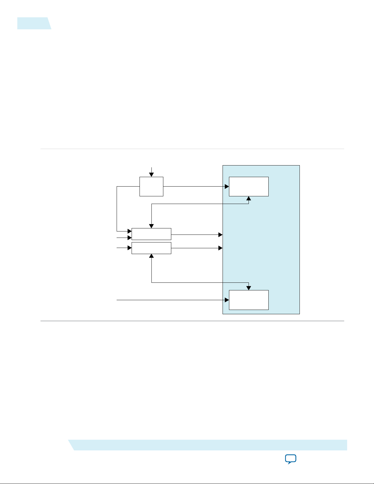
L1
xcvr_txdataout
Registers
L1
Inband
Slow
C&M
Fast
C&M
Vendor
Specific
L1
Control and Status
Interface
VSS
Interface
Interface
to Reset Controllers
Interface
to TX PLL
Transmitter
xcvr_rxdatain
CPRI Interface (CPRI Link)
Receiver
Multiplexing
Access to
Ctrl_AxC bytes
in CPRI frame
Access to
IQ Data
in CPRI frame
Full access
to
CPRI frame
Real-Time
Vendor
Specific
HDLC
Serial
Ethernet
PCS
Ctrl_AxC
Interface
RTVS
Interface
Direct IQ
Interface
Transceiver
Reconfiguration
Interface
Dedicated access to specific parts of CPRI frame
AUX
Interface
MII
Software
Interface
www.altera.com
101 Innovation Drive, San Jose, CA 95134
Functional Description
3
UG-01156
Subscribe
The Altera CPRI v6.0 IP core implements Layer 1 of the CPRI V6.0 specification and provides optional
CPRI V6.0 Layer 2 access points through various interfaces.
Interfaces Overview
Figure 3-1: CPRI v6.0 IP Core Interfaces
The IP core assembles the outbound CPRI frame control words and data from all of these interfaces, and
unloads and routes control words and data from the inbound CPRI frame to the appropriate interfaces,
based on configuration and register settings. With parameter settings, you control the presence or absence
of the AUX interface, the L1 control and status interface, and each of the interfaces that provide dedicated
access to specific parts of the CPRI frame. In contrast, the CPRI interface, the transceiver interfaces, and
the software interface to the IP core registers are always implemented.
Send Feedback
©
2015 Altera Corporation. All rights reserved. ALTERA, ARRIA, CYCLONE, ENPIRION, MAX, MEGACORE, NIOS, QUARTUS and STRATIX words and logos are
trademarks of Altera Corporation and registered in the U.S. Patent and Trademark Office and in other countries. All other words and logos identified as
trademarks or service marks are the property of their respective holders as described at www.altera.com/common/legal.html. Altera warrants performance
of its semiconductor products to current specifications in accordance with Altera's standard warranty, but reserves the right to make changes to any
products and services at any time without notice. Altera assumes no responsibility or liability arising out of the application or use of any information,
product, or service described herein except as expressly agreed to in writing by Altera. Altera customers are advised to obtain the latest version of device
specifications before relying on any published information and before placing orders for products or services.
ISO
9001:2008
Registered
Page 32

3-2
Interfaces Overview
UG-01156
2014.08.18
Multiple interfaces control the contents of the outbound CPRI frame control words and data. The CPRI
v6.0 implements the following transmission priorities among these interfaces:
• CPRI frame control words:
1. If the IP core implements the AUX interface, the AUX interface aux_tx_data bus, with appropriate
delay, has first priority in filling in the outbound CPRI frame control words.
2. If the IP core does not implement the AUX interface, or the aux_tx_mask value associated with the
relevant incoming data blocks the relevant aux_tx_data bits, each of the following interfaces, if
implemented, has secondary priority in filling the relevant part of the outbound CPRI frame
control words:
• Real-time vendor specific interface (RTVS)
• Vendor specific interface (VS)
• AxC control information interface (Ctrl_AxC)
3. For any part of the CPRI frame control words not filled in by one of the previous methods, the
transmission-enabled values most recently written to the control transmit table through the full
control word access registers CTRL_INDEX and TX_CTRL determine the contents of the outbound
CPRI frame control words. If the most recently written word for a CPRI frame position is not
transmission-enabled, no transmission is authorized from the control transmit table to that CPRI
frame position.
4. If none of the previous methods provides the content for a position in the CPRI frame control
word, the following interfaces, if implemented have the lowest priority in filling the relevant part of
the outbound CPRI frame control words:
• Fast control and management (Ethernet) MII interface
• Slow control and management (HDLC) serial interface
• L1 control and status interface
• Dedicated registers that contain or control content for control word positions in the CPRI
frame. For example, the rx_prot_ver_filter field of the PROT_VER register
• Transmission of special symbols according to the CPRI protocol. For example, K28.5, D16.2, /S/,
or /T/
• CPRI frame I/Q data words:
1. If the IP core implements the AUX interface, the AUX interface aux_tx_data bus, with appropriate
delay, has first priority in filling in the outbound CPRI frame I/Q data words.
2. If the IP core does not implement the AUX interface, or the aux_tx_mask value associated with the
relevant incoming data blocks the relevant aux_tx_data bits, the Direct I/Q interface, if
implemented, has secondary priority in filling the relevant part of the outbound CPRI frame I/Q
data words.
Altera Corporation
Functional Description
Send Feedback
Page 33

TX PLL
Standard TX PCS
10G TX PCS
TX
PMA
Standard RX PCS
10G RX PCS
RX
PMA
Native PHY IP Core
CPRI v6.0 IP Core
cpu_clk
mii_rxclk
mii_txclk
clk_ex_delay cpri_10g_coreclk
reconfig_clk
xcvr_ext_pll_clk
xcvr_recovered_clk
xcvr_cdr_refclk
cpri_clkout
External Clean-Up PLL
(in slave mode only)
CPU Interface
Extended Delay Measurement
MII
FIFO
FIFO
UG-01156
2014.08.18
CPRI v6.0 IP Core Clocking Structure
Figure 3-2: CPRI v6.0 IP Core Clocking Structure
Illustrates the clocks and clock domains in the CPRI v6.0 IP core. Clock domains shown are cpri_clkout,
clk_ex_delay, cpu_clk, and mii_{rx,tx}clk. The external clean-up PLL is only required in slave
clocking mode.
CPRI v6.0 IP Core Clocking Structure
3-3
Table 3-1: CPRI v6.0 IP Core Input Clocks
Functional Description
The main CPRI v6.0 IP core clock is cpri_clkout.
CPRI v6.0 Input Clock Information
xcvr_ext_pll_clk
Clocks the transmitter PMA.
You should drive this input clock with the output of the external TX
PLL. In Arria 10 devices, the frequency of this clock must be one
half the CPRI line bit rate. You must configure a PLL IP core that is
capable of driving the required frequency.
xcvr_cdr_refclk Receiver CDR reference clock. You must drive this clock at the
frequency you specified for the Supported receiver CDR frequency
(MHz) parameter in the CPRI v6.0 parameter editor.
reconfig_clk
In Stratix V and Arria V GZ variations, clock for CPRI v6.0 IP core
transceiver start-up and reconfiguration.
In Arria 10 variations, clocks the signals on the CPRI v6.0
transceiver reconfiguration interface.
ex_delay_clk Clock for extended delay measurement.
The supported frequency range of this clock is 100–150 MHz.
Altera Corporation
Send Feedback
Page 34

3-4
CPRI v6.0 IP Core Clocking Structure
CPRI v6.0 Input Clock Information
UG-01156
2014.08.18
cpri_10g_coreclk
Drives the CPRI v6.0 IP core clock cpri_clkout when the IP core
is running at the CPRI line bit rate of 10.1376 Gbps.
You must drive this clock at 307.20 MHz.
You must drive this clock from the same clock source as the xcvr_
ext_pll_clk input signal to the IP core.
cpu_clk Clocks the signals on the CPRI v6.0 CPU interface. Supports any
frequency that the device fabric supports.
mii_txclk mii_txclk clocks the MII transmitter interface and mii_rxclk
mii_rxclk
clocks the MII receiver interface. You must drive these clocks at the
frequency of 25 MHz to achieve the 100 Mbps bandwidth required
for this interface.
These clocks are present only if you turn on Enable IEEE 802.3
100BASE-X 100Mbps MII in the CPRI v6.0 parameter editor.
Table 3-2: CPRI v6.0 IP Core Output Clocks
CPRI v6.0 Output Clock Information
cpri_clkout
Master clock for the CPRI v6.0 IP core. When the IP core is
running at the CPRI line bit rate of 10.1376 Gbps, the cpri_10g_
coreclk input clock drives cpri_clkout. At all other CPRI line bit
rates, the Tx PCS drives cpri_clkout.
The frequency of cpri_clkout depends on the CPRI line bit rate:
CPRI Line Bit Rate cpri_clkout Frequency
0.6144 Gbps 15.36 MHz
1.2288 Gbps 30.72 MHz
2.4576 Gbps 61.44 MHz
3.0720 Gbps 76.80 MHz
4.9152 Gbps 122.88 MHz
6.1440 Gbps 153.60 MHz
9.8304 Gbps 245.76 MHz
10.1376 Gbps 307.20 MHz
xcvr_recovered_clk Direct recovered clock from the receiver CDR. Use this output
clock to drive the external clean-up PLL when your IP core is in
slave mode.
Related Information
Adding the Clean-Up PLL on page 2-12
Altera Corporation
Functional Description
Send Feedback
Page 35

UG-01156
2014.08.18
CPRI v6.0 IP Core Reset Requirements
CPRI v6.0 IP Core Reset Requirements
To reset the entire CPRI v6.0 IP core, you must assert the reset signals to the required external reset
controller logic. If you instantiate two Altera PHY Reset Controllers to implement this logic, one for the
TX data path and one for the RX data path, the user guide refers to the reset input signals to the two reset
controllers as reset_tx and reset_rx. Each of these two reset signals causes the reset logic to reset the
relevant data path of the IP core. However, the two signals are not direct input signals to the CPRI v6.0 IP
core.
In addition, some individual interfaces to the IP core have their own reset signals to reset only the
associated interface and logic.
Table 3-3: CPRI v6.0 IP Core Reset Signals
You can assert all reset signals asynchronously to any clock. However, you must hold each reset signal asserted for
one full clock period of its associated clock, to ensure it is captured by the IP core.
3-5
CPRI v6.0 IP Core Reset Signal Polarity Associated
Clock
xcvr_tx_analogreset Active high Analog reset to transmitter from external
Information
reset controller.
xcvr_tx_digitalreset Active high Digital reset to transmitter from external
reset controller.
xcvr_rx_analogreset Active high
Analog reset to receiver from external
reset controller.
xcvr_rx_digitalreset Active high Digital reset to receiver from external
reset controller.
ex_delay_reset Active low ex_delay_
clk
reconfig_reset Active high reconfig_
clk
Resets the extended delay measurement
block.
Asynchronous reset signal. Resets the
CPRI v6.0 Arria 10 transceiver reconfigu‐
ration interface and all of the registers to
which it provides access.
cpu_reset Active low cpu_clk Resets the CPRI v6.0 CPU interface and
all of the registers to which it provides
access.
mii_txreset Active low mii_txclk Resets the MII transmitter interface and
FIFO write logic.
mii_rxreset Active low mii_rxclk Resets the MII receiver interface and
Functional Description
Send Feedback
FIFO read logic.
Altera Corporation
Page 36

Reset Controller
Reset Controller
TX
PLL
Transmitter
(Native PHY)
Receiver
(Native PHY)
User-Defined
Reference Clock
xcvr_ext_pll_clk
xcvr_tx_analogreset
xcvr_tx_digitalreset
xcvr_tx_cal_busy
xcvr_rx_analogreset
xcvr_rx_digitalreset
xcvr_rx_is_lockedtodata
xcvr_rx_cal_busy
xcvr_cdr_refclk
reset_tx
reset_rx
pll_locked
CPRI v6.0 IP Core
xcvr_reset_tx_ready
xcvr_reset_rx_ready
3-6
Start-Up Sequence Following Reset
Figure 3-3: Required External Blocks
An example showing how you could connect required components to a single CPRI v6.0 IP core.
UG-01156
2014.08.18
To reset the CPRI v6.0 IP core, you must trigger the reset controller logic by asserting the active low
reset_tx and reset_rx input signals. When you trigger the reset controllers, they should deassert the
xcvr_reset_tx_ready and xcvr_reset_rx_ready input ready signals to the IP core. After each reset
controller completes resetting the transceiver and IP core data path, it should assert the relevant ready
signal.
Related Information
Integrating Your IP Core in Your Design: Required External Blocks on page 2-11
Shows main data path reset signals and how the reset controller connects to the IP core.
Start-Up Sequence Following Reset
After reset, if you turned on Enable start-up sequence state machine in the CPRI v6.0 IP core, the
internal state machine performs link synchronization and other initialization tasks. If you did not turn on
Enable start-up sequence state machine, user logic must perform these functions.
Altera Corporation
Functional Description
Send Feedback
Page 37

UG-01156
2014.08.18
Table 3-4: Start-Up Sequence Interface Signals
All interface signals are clocked by the cpri_clkout clock.
Signal Name Direction Description
state_startup_seq[2:0] Output Indicates the state of the CPRI start-up sequence state
Start-Up Sequence Following Reset
machine. This signal has the following valid values:
• 3'b000: State A: Standby
• 3'b001: State B: L1 Synchronization
• 3'b011: State C: Protocol Setup
• 3'b010: State D: Control and Management Setup
• 3'b110: State E: Interface and VSS Negotiation
• 3'b111: State F: Operation
• 3'b101: State G: Passive Link
This signal is available only if you turn on Enable start-up
sequence state machine in the CPRI v6.0 parameter
editor.
3-7
state_l1_synch[2:0]
Output State B condition indicator. Indicates the state of the CPRI
receiver L1 synchronization state machine. This signal has
the following valid values:
• 3'b000: XACQ1
• 3'b001: XACQ2
• 3'b011: XSYNC1
• 3'b010: XSYNC2
• 3'b110: HFNSYNC
nego_bitrate_complete Input Indicates the CPRI line bit rate negotiation is complete.
Input from external CPRI line bit rate negotiation block.
If you do not turn on Enable auto-rate negotiation in the
CPRI v6.0 parameter editor, you should tie this signal
high.
This signal is available only if you turn on Enable start-up
sequence state machine in the CPRI v6.0 parameter
editor.
Asserting this signal advances the start-up sequence state
machine from state B to state C. The IP core writes the
value of this signal to the nego_bitrate_complete field of
the START_UP_SEQ register at offset 0x24.
Functional Description
Send Feedback
Altera Corporation
Page 38

3-8
Start-Up Sequence Following Reset
Signal Name Direction Description
UG-01156
2014.08.18
nego_protocol_complete Input
nego_cm_complete Input
nego_vss_complete Input
Indicates the CPRI protocol version negotiation is
complete.
This signal is available only if you turn on Enable start-up
sequence state machine in the CPRI v6.0 parameter
editor.
Asserting this signal advances the start-up sequence state
machine from state C to state D. The IP core writes the
value of this signal to the nego_protocol_complete field
of the START_UP_SEQ register at offset 0x24.
Indicates the Control and Management negotiation is
complete.
This signal is available only if you turn on Enable start-up
sequence state machine in the CPRI v6.0 parameter
editor.
Asserting this signal advances the start-up sequence state
machine from state D to state E. The IP core writes the
value of this signal to the nego_cm_complete field of the
START_UP_SEQ register at offset 0x24.
Indicates the Vendor Specific negotiation is complete.
This signal is available only if you turn on Enable start-up
sequence state machine in the CPRI v6.0 parameter
editor.
Asserting this signal advances the start-up sequence state
machine from state E to state F. The IP core writes the
value of this signal to the nego_vss_complete field of the
START_UP_SEQ register at offset 0x24.
nego_l1_timer_expired Input If you do not turn on Enable L1 inband protocol
negotiator in the CPRI v6.0 parameter editor, drive this
signal from your user-defined L1 timer to indicate that the
L1 timer has expired.
Note that if you do not turn on Enable L1 inband
protocol negotiator, user logic is expected to maintain an
L1 timer outside the IP core.
This signal is available only if you turn on Enable start-up
sequence state machine in the CPRI v6.0 parameter
editor.
If you also turn on Enable L1 inband protocol negotiator
in the CPRI v6.0 parameter editor, you should tie this
signal low so it does not interfere with the internal L1
timer.
Altera Corporation
Functional Description
Send Feedback
Page 39

000 111 110 101001 011
000
001
011 111 110
cpri_clkout
state_startup_sequence
state_l1_sync
nego_bitrate_complete
nego_vss_complete
Bit Rate
Negotiation
Protocol Version
Negotiation
Control and Management Rate
Negotiation
VSS and Interface
Negotiation
Operational
Mode
UG-01156
2014.08.18
Figure 3-4: Start-Up Sequence State Machine Timing Diagram
AUX Interface
AUX Interface
3-9
The CPRI v6.0 IP core auxiliary (AUX) interface provides direct access to the CPRI 10 ms radio frame,
including I/Q data and control words. You can use this interface to support your specific application. For
example, the AUX interface allows you to implement custom I/Q sample widths and custom mapping
schemes.
The AUX interface also enables multi-hop routing applications and provides timing reference informa‐
tion for transmitted and received frames. Using this interface, you can load I/Q data in a precise location
in the precise CPRI basic frame you target.
The AUX interface allows you to connect CPRI v6.0 IP core instances and other system components
together by supporting a direct connection to a user-defined routing layer or custom mapping block. You
implement this routing layer, which is not defined in the CPRI V6.0 Specification, outside the CPRI v6.0
IP core. The AUX interface supports the transmission and reception of I/Q data and timing information
between an RE slave and an RE master, allowing you to define a custom routing layer that enables daisychain configurations of RE master and slave ports. Your custom routing layer determines the I/Q sample
data to pass on to other REs to support multi-hop network configurations and custom mapping
algorithms.
If you turn on Enable auxiliary interface in the CPRI v6.0 parameter editor, your IP core includes this
interface.
Functional Description
Send Feedback
Altera Corporation
Page 40

3-10
AUX Interface Signals
AUX Interface Signals
Table 3-5: AUX Interface Signals
If you turn on Enable auxiliary interface in the CPRI v6.0 parameter editor, the AUX interface is available. This
interface allows access to the entire CPRI frame and has the highest priority among the L1 interfaces.
You can alter the transmit write latency with the Auxiliary latency cycle(s) parameter. The default transmit
latency, when Auxiliary latency cycle(s) has the value of zero, is one cpri_clkout cycle. You can specify
additional latency cycles.
All interface signals are clocked by the cpri_clkout clock.
AUX RX Interface Status Signals
Signal Name Direction Description
aux_rx_rfp Output Synchronization pulse for start of 10 ms radio frame. The
pulse occurs at the start of the radio frame on the AUX RX
interface.
aux_rx_hfp Output Synchronization pulse for start of hyperframe. The pulse
occurs at the start of the hyperframe on the AUX RX
interface.
UG-01156
2014.08.18
aux_rx_bfn[11:0] Output Current radio frame number on the AUX RX interface.
aux_rx_z[7:0] Output Current hyperframe number on the AUX RX interface.
Value is in the range 0–149.
aux_rx_x[7:0] Output Index number of the current basic frame in the current
hyperframe on the AUX RX interface. Value is in the
range 0–255.
aux_rx_seq[6:0] Output Index number of the current 32-bit word in the current
basic frame on the AUX RX interface. The value range
depends on the current CPRI line bit rate:
• 0.6144 Gbps: range is 0–3
• 1.2288 Gbps: range is 0–7
• 2.4576 Gbps: range is 0–15
• 3.0720 Gbps: range is 0–19
• 4.9152 Gbps: range is 0–31
• 6.1440 Gbps: range is 0–39
• 9.8304 Gbps: range is 0–63
• 10.1376 Gbps: range is 0–79
AUX RX Interface Data Signals
Signal Name Direction Description
aux_rx_data[31:0] Output Data the IP core presents on the AUX link. Data is
Altera Corporation
transmitted in 32-bit words. Byte [31:24] is transmitted
first and byte [7:0] is transmitted last.
Functional Description
Send Feedback
Page 41

UG-01156
2014.08.18
AUX Interface Signals
AUX RX Interface Data Signals
Signal Name Direction Description
aux_rx_ctrl[3:0] Output Control slots indicator. Each asserted bit indicates that the
3-11
corresponding byte position in aux_rx_data holds a byte
from a CPRI control word.
AUX TX Interface Control and Status Signals
Signal Name Direction Description
aux_tx_sync_rfp Input Synchronization input used in REC master to control the
start of a new 10 ms radio frame. Asserting this signal
resets the frame synchronization machine. The CPRI v6.0
IP core uses the rising edge of the pulse for synchroniza‐
tion.
aux_tx_err[3:0] Output Indicates that in the previous cpri_clkout cycle, aux_tx_
mask bits masked one or more control words in the target
CPRI frame.
aux_tx_rfp Output Synchronization pulse for start of 10 ms radio frame. The
pulse occurs at the start of the radio frame on the AUX TX
interface.
aux_tx_hfp Output Synchronization pulse for start of hyperframe. The pulse
occurs at the start of the hyperframe on the AUX TX
interface.
aux_tx_bfn[11:0] Output Current radio frame number on the AUX TX interface.
aux_tx_z[7:0] Output Current hyperframe number on the AUX TX interface.
Value is in the range 0–149.
aux_tx_x[7:0] Output Index number of the current basic frame in the current
hyperframe on the AUX TX interface. Value is in the
range 0–255.
aux_tx_seq[6:0] Output Index number of the current 32-bit word in the current
basic frame on the AUX TX interface.
The value range depends on the current CPRI line bit rate:
• 0.6144 Gbps: range is 0–3
• 1.2288 Gbps: range is 0–7
• 2.4576 Gbps: range is 0–15
• 3.0720 Gbps: range is 0–19
• 4.9152 Gbps: range is 0–31
• 6.1440 Gbps: range is 0–39
• 9.8304 Gbps: range is 0–63
• 10.1376 Gbps: range is 0–79
Functional Description
Send Feedback
Altera Corporation
Page 42

3-12
AUX Interface Signals
AUX TX Interface Data Signals
Signal Name Direction Description
aux_tx_data[31:0] Input Data the IP core receives on the AUX TX interface. The
data is aligned with aux_tx_seq with a write delay of one
cpri_clkout cycle plus the number of additional cpri_
clkout cycles you specify as the value of the Auxiliary
latency cycle(s) parameter.
User logic is responsible to ensure that the write data in
aux_tx_data is aligned with the write latency value of the
Auxiliary latency cycle(s) parameter.
Data is received in 32-bit words. For correct transmission
in the CPRI frame, you must send byte [31:24] first and
byte [7:0] last.
UG-01156
2014.08.18
aux_tx_mask[31:0]
aux_tx_ctrl[3:0]
Input Bit mask for insertion of data from aux_tx_data in the
target CPRI frame.
This signal aligns with aux_tx_data and therefore, aligns
with aux_tx_seq with a delay of one cpri_clkout cycle
plus the number of additional cpri_clkout cycles you
specify as the value of the Auxiliary latency cycle(s)
parameter.
Assertion of a bit in this mask overrides insertion of data
to the corresponding bit in the target CPRI frame from
any other source. Therefore, you must deassert the mask
bits during K28.5 character insertion in the outgoing
CPRI frame, which occurs when Z=X=0. If you do not
deassert the mask bits during K28.5 character insertion in
the outgoing CPRI frame, the aux_tx_err output signal is
asserted in the following cpri_clkout cycle.
Output Control slots indicator. Each asserted bit indicates that the
corresponding byte position, as indicated by aux_tx_seq,
should hold a CPRI control word in the target CPRI
frame.
Altera Corporation
Functional Description
Send Feedback
Page 43

4095 0
0
3
255 1
149 0
2 0 1 2 3 0 1 2
X Data #1 Data #2 Data #3 Data #4 Data #5
cpri_clkout
aux_rx_rfp
aux_rx_bfn
aux_rx_hfp
aux_rx_z
aux_rx_x
aux_rx_seq
aux_rx_data
aux_rx_ctrl[3:0]
Data #6
0000 1000
0000
Data #7
X 1000
21 22
216
3
215 1
98 0
2 0 1 0 1 2 3 0
cpri_clkout
aux_tx_rfp
aux_tx_bfn
aux_tx_hfp
aux_tx_hfn
aux_tx_x
aux_tx_seq
aux_tx_sync_rfp
0
UG-01156
2014.08.18
Figure 3-5: AUX RX Interface Timing Diagram
AUX RX interface behavior in a CPRI v6.0 IP core running at 0.6144 Gbps.
AUX Interface Signals
3-13
Figure 3-6: CPRI REC Master Response to aux_tx_sync_rfp Resynchronization Pulse
Asserting aux_tx_sync_rfp resets the hyperframe and basic frame numbers in an REC master CPRI v6.0
IP core. Shown for a CPRI v6.0 IP core running at 0.6144 Gbps.
Functional Description
Send Feedback
Altera Corporation
Page 44

clock cycles write latency
4095 0
0
3
255 1
149 0
2 0 1 2 3 0 1 2
X Data #1 Data #2 Data #3 Data #4 Data #5
Data #5
X Mask #1 Mask #2 Mask #3 Mask #4 Mask #5
0 1 2 3 0 01 2 3
X Data #1 Data #2 Data #3 Data #4
cpri_clkout
aux_tx_rfp
aux_tx_bfn
aux_tx_hfp
aux_tx_hfn
aux_tx_x
aux_tx_seq
aux_tx_data
aux_tx_mask
Sequence Nnumber
at actual CPRI frame
Actual frame data
Default one cpri_clkout cycle
delay to write
Default delay + 1
Auxiliary latency cycle(s) == 1:
3-14
AUX Interface Signals
Figure 3-7: AUX TX Interface Timing Diagram with One Auxiliary Latency Cycle
Expected behavior on the AUX TX interface of a CPRI v6.0 IP core running at 0.6144 Gbps. Illustrates the
effect of setting the Auxiliary latency cycle(s) parameter to a a non-zero value. Shown for a CPRI v6.0 IP
core with Auxiliary latency cycle(s) set to the value of 1.
UG-01156
2014.08.18
Altera Corporation
Functional Description
Send Feedback
Page 45

clock cycles write latency
4095 0
0
3
255 1
149 0
2 0 1 2 3 0 1 2
X Data #1 Data #2 Data #3 Data #4 Data #5
Data #5
X Mask #1 Mask #2 Mask #3 Mask #4 Mask #5
0 1 2 3 0 01 2 3
X Data #1 Data #2 Data #3 Data #4
cpri_clkout
aux_tx_rfp
aux_tx_bfn
aux_tx_hfp
aux_tx_hfn
aux_tx_x
aux_tx_seq
aux_tx_data
aux_tx_mask
Sequence Nnumber
at actual CPRI frame
Actual frame data
Default one cpri_clkout cycle
delay to write
Default delay + 4
Auxiliary latency cycle(s) == 1:
UG-01156
2014.08.18
AUX Interface Signals
Figure 3-8: AUX TX Interface Timing Diagram with Four Auxiliary Latency Cycles
Expected behavior on the AUX TX interface of a CPRI v6.0 IP core running at 0.6144 Gbps. Illustrates the
effect of setting the Auxiliary latency cycle(s) parameter to the value of four.
3-15
Functional Description
Send Feedback
Altera Corporation
Page 46

4095 0
0
3
255 1
149 0
2 0 1 2 3 0 1 2
X Data #1 Data #2 Data #3 Data #4 Data #5
cpri_clkout
aux_tx_rfp
aux_tx_bfn
aux_tx_hfp
aux_tx_hfn
aux_tx_x
aux_tx_seq
aux_tx_data
aux_tx_mask
Auxiliary latency cycle(s) == 0
Data #6
X Mask #1 Mask #2 Mask #3 Mask #4 Mask #5 Mask #6
0000 1000 0000 1000 0000
aux_tx_err
aux_tx_ctrl[3:0]
3-16
AUX Interface Signals
Figure 3-9: AUX TX Timing Diagram with Error
Illustrates the behavior of the aux_tx_err signal on the AUX TX interface of a CPRI v6.0 IP core running
at 0.6144 Gbps. The aux_tx_ctrl signal shows that when aux_tx_seq has the value of zero, the first byte
at the corresponding position in the target CPRI frame is a control byte. The value of the Auxiliary latency
cycle(s) parameter is zero. Therefore, the data on aux_tx_data is delayed by one clock cycle from the
value on aux_tx_seq. The data that appears on aux_tx_data when aux_tx_seq has the value of 1 is the
data that targets position X.Y.Z.0 in the target CPRI frame.
The value of Mask #1 is presumably 0xFFXXXXXX, indicating that the incoming data on aux_tx_data is
intended to overwrite this control byte in the target CPRI frame. Therefore, in the following cpri_clkout
cycle, the IP core asserts the aux_tx_err signal.
UG-01156
2014.08.18
Related Information
• AUX Interface Synchronization on page 3-17
Illustrates the relationship between the AUX synchronization signals.
• Auxiliary Latency Cycles on page 3-17
The Auxiliary latency cycle(s) parameter affects the relative timing of the data on the aux_tx_data and
aux_tx_mask busses. This section provides an explanation of the parameter's effect and purpose.
Altera Corporation
Functional Description
Send Feedback
Page 47

aux_{rx,tx}_rfp
aux_{rx,tx}_bfn
aux_{rx,tx}_hfp
aux_{rx,tx}_z
aux_{rx,tx}_x
aux_{rx,tx}_seq
0 1 ...
NUM_SEQ - 1
2 ...
...210
255
149
10
n n + 1 n + 2
Hyperframe
Radio Frame (10 ms)
Basic Frame
UG-01156
2014.08.18
AUX Interface Synchronization
Figure 3-10: Relationship Between Synchronization Pulses and Numbers on the AUX Interface
The output synchronization signals are useful for custom user logic, including frame synchronization
across hops in multi-hop configurations.
The output synchronization signals are derived from the CPRI frame synchronization state machine.
AUX Interface Synchronization
3-17
Functional Description
Related Information
AUX Interface Signals on page 3-10
Describes the AUX interface signals and provides AUX interface timing diagrams.
Auxiliary Latency Cycles
Altera provides configurable write latency on the AUX TX interface and other direct TX interfaces to
support user logic with sufficient advance notice of the position in the CPRI frame. The processing time
that user logic requires after determining the current position in the CPRI frame is implementation
specific, and the default write latency of a single cpri_clkout cycle might not be adequate. Using the
Auxiliary latency cycle(s) parameter, you can set the write latency to the number of clock cycles required
for your system to process data before sending it on the AUX TX interface or other direct TX interface.
Send Feedback
Altera Corporation
Page 48

aux_tx_seq[5:0]
internal tx_seq value[5:0]
CPRI Frame
210 3
3939 38
38
Ct rl Ct rl {Ctrl,feed}
0 1 2 3
393839
aux_tx_mask[31:0]
aux_tx_data[31:0]
0000ffff ffffffff
00000000 00000000 ffffffff ffffffff
0000feed abcdabcd
abcdabcd
00000000 00000000
1 cpri_clkout cycle
default write latency
3-18
Direct Interface CPRI Frame Data Format
In the CPRI v6.0 parameter editor, you can specify a non-zero number of Auxiliary latency cycle(s) to
increase the write latency on the AUX TX interface and other direct TX interfaces to the CPRI v6.0 IP
core.
The write latency is the number of cpri_clkout cycles from when the aux_tx_seq output signal has the
value of n to when user logic must write data to the AUX TX interface to target the corresponding
position in the CPRI frame. For other direct interfaces, the IP core notifies user logic when it is ready for
input and the user does not need to monitor the aux_tx_seq signal. However, the Auxiliary latency
cycle(s) value does apply to all of the direct interfaces.
When Auxiliary latency cycle(s) has the default value of zero, the write latency on the direct TX interfaces
is one cpri_clkout cycle. When Auxiliary latency cycle(s) has the value of N, the write latency is (1+N)
cpri_clkout cycles.
User logic is responsible to ensure that the data presented to the IP core on the AUX TX interface is
presented at the correct write latency relative to the AUX TX interface synchronization signals.
Note:
You cannot simply write to the AUX TX interface with a consistent write latency that you
determine after configuring your IP core. If you do not specify the correct write latency in the
CPRI v6.0 parameter editor, the data you present on the AUX TX interface will not fill the correct
position in the target CPRI frame. To ensure the write latency offset is implemented correctly in
the IP core, you must set the parameter.
Figure 3-11: AUX Interface Transmit Write Latency
UG-01156
2014.08.18
Illustrates the transmit write latency on the AUX interface when Auxiliary latency cycle(s) has the value
of 0. If you specify a non-zero value for this parameter, the latency increases from the default latency of
one cpri_clkout cycle to 1 plus the number of cycles you specify.
In this example, the CPRI line bit rate is 6.144 Gbps, so that the control word is 10 bytes. User logic masks
the control word, so that the IP core does not receive the control words from the AUX interface.
Direct Interface CPRI Frame Data Format
Altera Corporation
The information on the AUX interface and all of the other direct interfaces except the L1 CSR interface,
appears in the relevant data bus in 32-bit words. The CPRI v6.0 IP core converts the contents of the
incoming CPRI frame to a 32-bit format internally. Similarly, the IP core expects to receive data on the
Functional Description
Send Feedback
Page 49

0.6144 Gbps
Line Rate:
1.2288 Gbps
Line Rate:
2.4576 Gbps
Line Rate:
3.072 Gbps
Line Rate:
0 1 2 3
[31:24]
#Z .X.0 .0
(1)
#Z.X.4.0 #Z.X.8.0 #Z.X.12.0
[23:16] #Z.X.1.0 #Z.X.5.0 #Z.X.9.0 #Z.X.13.0
[15:8] #Z.X.2.0 #Z.X.6.0 #Z.X.10.0 #Z.X.14.0
[7:0] #Z.X.3.0 #Z.X.7.0 #Z.X.11.0 #Z.X.15.0
0 1 2 ... 7
[31:24]
#Z .X. 0.0
(1)
#Z.X.2.0 #Z.X.4.0 ... #Z.X.14.0
[23:16]
#Z .X. 0.1
(1)
#Z.X.2.1 #Z.X.4.1 ... #Z.X.14.1
[15:8] # Z.X.1.0 #Z.X.3. 0 #Z.X.5.0 ... #Z.X.15.0
[7:0] #Z.X.1.1 #Z.X.3.1 #Z.X.5.1 ... #Z.X.15.1
0 1 2 ... 15
[31:24]
#Z.X.0 .0
(1)
#Z.X.1.0 #Z.X.2.0 ... #Z.X.15.0
[23:16] #Z.X.0 .1
(1)
#Z.X.1.1 #Z.X.2.1 ... #Z.X.15.1
[15:8] # Z.X.0.2
(1)
#Z.X.1.2 #Z.X.2.2 ... #Z.X.15.2
[7:0] #Z.X.0.3
(1)
#Z.X.1.3 #Z.X.2.3 ... #Z.X.15.3
0 1 2 ... 18 19
[31:24] #Z.X.0.0
(1)
#Z.X.0.4
(1)
#Z.X.1.3 ... #Z.X.14.2 #Z.X.15.1
[23:16] #Z.X.0.1
(1)
#Z.X.1.0 #Z.X.1.4 ... #Z.X.14.3 #Z.X.15.2
[15:8] # Z.X.0.2
(1)
#Z.X.1.1 #Z.X.2.0 ... #Z.X.14.4 #Z.X.15.3
[7:0] #Z.X.0.3
(1)
#Z.X.1.2 #Z.X.2.1 ... #Z.X.15.0 #Z.X.15.4
Sequence number on AUX interface
Sequence number on AUX interface
Sequence number on AUX interface
Sequence number on AUX interface
UG-01156
2014.08.18
Direct Interface CPRI Frame Data Format
various direct interfaces in this format. The only exception is the L1 CSR interface, which transmits and
receives information in individual bits.
Figure 3-12: AUX Interface Data at Different CPRI Line Bit Rates
The AUX interface presents and expects data in fixed 32-bit words. The mapping of the CPRI frame to
and from 32-bit words depends on the CPRI v6.0 IP core bit rate. This figure illustrates how CPRI frame
words are mapped to 32-bit words on the AUX interface 32-bit data bus.
3-19
Functional Description
Send Feedback
Altera Corporation
Page 50

0 1 2 ... 3 0 31
[31:24] # Z.X.0.0
(1)
#Z.X.0.4
(1)
#Z.X.1.0 ... #Z.X.14.0 #Z.X.15 .4
[23:16] # Z.X.0.1
(1)
#Z.X.0.5
(1)
#Z.X.1.1 ... #Z.X.14.1 #Z.X.15 .5
[15:8] # Z.X.0.2
(1)
#Z.X.0.6
(1)
#Z.X.2.2 ... #Z.X.14.2 #Z.X.15 .6
[7:0] # Z.X.0.3
(1)
#Z.X.0.7
(1)
#Z.X.2.3 ... #Z.X.15.3 #Z.X.15 .7
0 1 2 ... 3 8 39
[31:24]
#Z.X.0 .0
(1)
#Z.X.0.4
(1)
#Z.X.0.8
(1)
... #Z.X.15.2 #Z.X.15.6
[23:16]
#Z.X.0 .1
(1)
#Z.X.0.5
(1)
#Z.X.0.9
(1)
... #Z.X.15.3 #Z.X.15.7
[15:8]
#Z.X.0 .2
(1)
#Z.X.0.6
(1)
#Z.X.1.0 ... #Z.X.15.4 #Z.X.15.8
[7:0]
#Z.X.0 .3
(1)
#Z.X.0.7
(1)
#Z.X.1.1 ... #Z.X.15.5 #Z.X.15.9
0 1 2 3 ... 62 63
[31:24]
#Z.X.0 .0
(1)
#Z.X.0.4
(1)
#Z.X.0.8
(1)
#Z.X.0.12
(1)
... #Z.X.15.8 #Z.X.15.12
[23:16]
#Z.X.0 .1
(1)
#Z.X.0.5
(1)
#Z.X.0.9
(1)
#Z.X.0.13
(1)
... #Z.X.15.9 #Z.X.15.13
[15:8]
#Z.X.0 .2
(1)
#Z.X.0.6
(1)
#Z.X.0.10
(1)
#Z.X.0.14
(1)
... #Z.X.15.1 0 #Z.X.15.14
[7:0]
#Z.X.0 .3
(1)
#Z.X.0.7
(1)
#Z .X. 0.11
(1)
#Z.X.0.15
(1)
... #Z.X.15.1 1 #Z.X.15.15
0 1 2 3 62 79
[31:24]
#Z.X.0 .0
(1)
#Z.X.0.4
(1)
#Z.X.0.8
(1)
#Z.X.0.12
(1)
...
[23:16]
#Z.X.0 .1
(1)
#Z.X.0.5
(1)
#Z.X.0.9
(1)
#Z.X.0.13
(1)
...
[15:8]
#Z.X.0 .2
(1)
#Z.X.0.6
(1)
#Z.X.0.10
(1)
#Z.X.0.14
(1)
...
[7:0]
#Z.X.0 .3
(1)
#Z.X.0.7
(1)
#Z .X. 0.11
(1)
#Z.X.0.15
(1)
...
#Z.X.0.16
#Z.X.0.17
#Z.X.0.18
#Z.X.0.19
#Z.X.1.0
#Z.X.1.1
#Z.X.1.2
#Z.X.1.3
4 5 ...
#Z.X.15.12
#Z.X.15.13
#Z.X.15.14
#Z.X.15.15
#Z.X.15.16
#Z.X.15.17
#Z.X.15.18
#Z.X.15.19
4.952 Gbps
Line Rate:
Sequence number on AUX interface
6.144 Gbps
Line Rate:
Sequence number on AUX interface
9.8304 Gbps
Line Rate:
Sequence number on AUX interface
10.1376 Gbps
Line Rate:
Sequence number on AUX interface
Note:
(1) Light blue table cells indicate control word bytes. Yellow table cells indicate real-time vendor specific bytes. White table cells indicate data word bytes.
31 24 23 16 15 8 7 0
I[3]
Q[3]
I[2]
Q[2]
I[1]
Q[1]
I[0]
Q[0]
I[7]
Q[7]
I[6]
Q[6]
I[5]
Q[5]
I[4]
Q[4]
I[11]
Q[ 11]
I[10]
Q[10]
I[9]
Q[9]
I[8]
Q[8]
I[15]
Q[15]
I[14]
Q[14]
I[13]
Q[13]
I[12]
Q[12]
3-20
Direct Interface CPRI Frame Data Format
UG-01156
2014.08.18
The CPRI IP core passes the incoming AUX data through to the CPRI link unmodified. You must ensure
that the incoming AUX data bits already include any CRC values expected by the application at the other
end of the CPRI link.
Figure 3-13: Data Sample Order on aux_tx_data and aux_rx_data Buses
Illustrates how CPRI frame data is ordered in each 32-bit word.
Altera Corporation
Functional Description
Send Feedback
Page 51

UG-01156
2014.08.18
Direct IQ Interface
If you turn on Enable direct IQ mapping interface in the CPRI v6.0 parameter editor, the direct IQ
interface is available. This interface allows direct access to the I/Q data time slots in the CPRI frame. You
can connect this interface to any user-defined air standard I/Q mapping module.
This interface is Avalon-ST compliant with a read latency value of 1.
You can alter the transmit latency with the Auxiliary latency cycle(s) parameter.
Table 3-6: Direct IQ Interface Signals
All interface signals are clocked by the cpri_clkout clock.
Signal Name Direction Description
iq_rx_valid[3:0] Output Each asserted bit indicates the corresponding byte on the
iq_rx_data[31:0] Output I/Q data received from the CPRI frame. The iq_rx_valid
Direct IQ Interface
Direct IQ RX Interface
current iq_rx_data bus is valid I/Q data.
signal indicates which bytes are valid I/Q data bytes.
3-21
Direct IQ TX Interface
Signal Name Direction Description
iq_tx_ready[3:0] Output Each asserted bit indicates the IP core is ready to read I/Q
data from the corresponding byte of iq_tx_data on the
next clock cycle.
iq_tx_valid[3:0] Input Write valid for iq_tx_data. Assert bit [n] to indicate that
the corresponding byte on the current iq_tx_data bus is
valid I/Q data.
iq_tx_data[31:0] Input I/Q data to be written to the CPRI frame. The IP core
writes the individual bytes of the current value on the iq_
tx_data bus to the CPRI frame based on the iq_tx_ready
signal from the previous cycle, and the iq_tx_valid
signal in the current cycle.
Functional Description
Send Feedback
Altera Corporation
Page 52

cpri_clkout
aux_rx_x[7:0]
aux_rx_seq[6:0]
iq_rx_valid[3:0]
2
3
4
2 3 0 1 2 3 0 1 2 3
1111 0111 1111 0111 1111
(IQ)(IQ) (IQ)(IQ)(IQ)(IQ) X(IQ)(IQ)(IQ) (IQ)(IQ)(IQ)(IQ) (IQ)(IQ)(IQ)(IQ) (IQ)(IQ)(IQ)(IQ) X(IQ)(IQ)(IQ) (IQ)(IQ)(IQ)(IQ) (IQ)(IQ)(IQ)(IQ) (IQ)(IQ)(IQ)(IQ)iq_rx_data[31:0]
cpri_clkout
aux_tx_x[7:0]
aux_tx_seq[6:0]
iq_tx_ready[3:0]
iq_tx_valid[3:0]
2 3 4
2 3 0 1 2 3 0 1 2 3
1111 0111 1111 0111 1111
1111 0111 1111 0111 1111
(IQ)(IQ) (IQ)(IQ)(IQ)(IQ) (IQ)(IQ)(IQ)(IQ) (IQ)(IQ)(IQ)(IQ) X(IQ)(IQ)(IQ) (IQ)(IQ)(IQ)(IQ) (IQ)(IQ)(IQ)(IQ) (IQ)(IQ)(IQ)(IQ) X(IQ)(IQ)(IQ) (IQ)(IQ)(IQ)(IQ)iq_tx_data[31:0]
Auxiliary latency cycle(s) == 1
3-22
Direct IQ Interface
Figure 3-14: Direct IQ RX Interface Timing Diagram
Direct IQ RX interface behavior in a CPRI v6.0 IP core running at 0.6144 Gbps.
The aux_rx_x and aux_rx_seq signals are not part of this interface and are available only if you turn on
the AUX interface in your CPRI v6.0 IP core variation. However, their presence in the timing diagram
explains the timing of the iq_rx_valid output signal that you use to identify the clock cycles with valid
I/Q data.
UG-01156
2014.08.18
Figure 3-15: Direct IQ TX Interface Timing Diagram
Expected behavior on the direct IQ TX interface of a CPRI v6.0 IP core running at 0.6144 Gbps.
The aux_tx_x and aux_tx_seq signals are not part of this interface and are available only if you turn on
the AUX interface in your CPRI v6.0 IP core variation. However, their presence in the timing diagram
explains the timing of the iq_tx_ready output signal that you use to identify the clock cycles when you
can write I/Q data to the CPRI frame. Note that the write latency is two cpri_clkout clock cycles in this
example.
Altera Corporation
Functional Description
Send Feedback
Page 53

UG-01156
2014.08.18
Related Information
Avalon Interface Specifications
For more information about the Avalon-ST protocol, including timing diagrams, refer to the Avalon
Streaming Interfaces chapter.
Direct Vendor Specific Access Interface
If you turn on Enable direct vendor specific access interface in the CPRI v6.0 parameter editor, the
direct vendor specific access interface is available. This interface allows direct access to the Vendor
Specific subchannels in the CPRI hyperframe. The Vendor Specific information is present only in
subchannels 16 through (P-1) of the CPRI hyperframe, where P is the Fast C&M pointer value. Check the
vs_rx_valid and vs_tx_ready signals to ensure you read and write this interface at the time that
corresponds to the correct position in the CPRI frame. If you implement the AUX interface, you can read
the value on the aux_rx_x or aux_tx_x output signal to identify the current position in the frame.
This interface is Avalon-ST compliant with a read latency value of 1.
You can alter the transmit latency with the Auxiliary latency cycle(s) parameter.
Table 3-7: Direct Vendor Specific Access Interface Signals
All interface signals are clocked by the cpri_clkout clock.
Direct Vendor Specific Access Interface
3-23
Direct Vendor Specific RX Interface
Signal Name Direction Description
vs_rx_valid[3:0] Output Each asserted bit indicates the corresponding byte on the
current vs_rx_data bus is a valid vendor-specific byte.
vs_rx_data[31:0] Output Vendor-specific word received from the CPRI frame. The
vs_rx_valid signal indicates which bytes are valid
vendor-specific bytes.
Direct Vendor Specific TX Interface
Signal Name Direction Description
vs_tx_ready[3:0] Output Each asserted bit indicates the IP core is ready to receive a
vendor-specific byte from the corresponding byte of vs_
tx_data on the next clock cycle.
vs_tx_valid[3:0] Input Write valid for vs_tx_data. Assert bit [n] of vs_tx_valid
to indicate that byte [n] on the vs_tx_data bus holds a
valid value in the current clock cycle.
vs_tx_data[31:0] Input Vendor-specific word to be written to the CPRI frame.
The IP core writes the individual bytes of the current value
on the vs_tx_data bus to the CPRI frame based on the
vs_tx_ready signal from the previous cycle, and the vs_
tx_valid signal in the current cycle.
Functional Description
Send Feedback
Altera Corporation
Page 54

cpri_clkout
79
80
81 124
125
15
16
17 60
61
0000 1000 000000001000
X (D2)XXX XX(D1)XXX
aux_rx_x
aux_rx_x[5:0]
vs_rx_valid[3:0]
vs_rx_data[31:0]
Pointer-P = 60
3-24
Direct Vendor Specific Access Interface
Figure 3-16: Direct VS RX Timing Diagram
Direct VS RX interface behavior in a CPRI v6.0 IP core running at 0.6144 Gbps.
The aux_rx_x signal is not part of this interface and is available only if you turn on the AUX interface in
your CPRI v6.0 IP core variation. However, its presence in the timing diagram explains the timing of the
vs_rx_valid output signal that you use to identify the clock cycles with valid VS data.
The aux_rx_x[7:0] signal (labelled simply aux_rx_x) holds the eight-bit index of the basic frame in the
hyperframe, from the perspective of the AUX interface. The subchannel index is the control word index
modulo 64, available in aux_rx_x[5:0] if you turn on the AUX interface in your CPRI IP core.
UG-01156
2014.08.18
Altera Corporation
Functional Description
Send Feedback
Page 55

cpri_clkout
79
80
81 124
125
15
16
17 60
61
0000 1000 000000001000
X 1000 XX1000
X (D2)XXX XX(D1)XXX
aux_tx_x
aux_tx_x[5:0]
vs_tx_ready[3:0]
vs_tx_valid[3:0]
vs_tx_data[31:0]
Auxiliary latency cycle(s) == 0
Pointer-P = 60
UG-01156
2014.08.18
Real-Time Vendor Specific Interface
Figure 3-17: Direct VS TX Timing Diagram
Expected behavior on the direct VS TX interface of a CPRI v6.0 IP core running at 0.6144 Gbps.
The aux_tx_x signal is not part of this interface and is available only if you turn on the AUX interface in
your CPRI v6.0 IP core variation. However, its presence in the timing diagram explains the timing of the
vs_tx_ready output signal that you use to identify the clock cycles when you can write VS data to the
CPRI frame.
The aux_tx_x[7:0] signal (labelled simply aux_tx_x) holds the eight-bit index of the basic frame in the
hyperframe, from the perspective of the AUX interface. The subchannel index is the control word index
modulo 64, available in aux_tx_x[5:0] if you turn on the AUX interface in your CPRI IP core.
Note that the write latency is one cpri_clkout clock cycle in this example.
3-25
Real-Time Vendor Specific Interface
Functional Description
Related Information
Avalon Interface Specifications
For more information about the Avalon-ST protocol, including timing diagrams, refer to the Avalon
Streaming Interfaces chapter.
If you turn on Enable real-time vendor specific interface (R-16A) in the CPRI v6.0 parameter editor, the
real-time vendor specific interface is available. This interface allows direct access to the Real Time Vendor
Specific words in the CPRI hyperframe. Check the rtvs_rx_valid and rtvs_tx_ready signals to ensure
you read and write this interface at the time that corresponds to the correct position in the CPRI frame. If
you implement the AUX interface, you can read the value on the aux_rx_seq or aux_tx_seq output
signal to identify the current position in the frame.
This option is only available if you specify a CPRI line bit rate of 10.1376 Gbps for your IP core.
This interface is Avalon-ST compliant with a read latency value of 1.
You can alter the transmit write latency with the Auxiliary latency cycle(s) parameter.
Altera Corporation
Send Feedback
Page 56

cpri_clkout
100 101 124
7
4
6
aux_rx_x
aux_rx_seq
rtvs_rx_valid
X
D1D2D3D4
Xrtvs_rx_data[31:0]
54
3
21
0
79
3
21
0
D5D6
X
3-26
Real-Time Vendor Specific Interface
Table 3-8: Real-Time Vendor Specific Interface Signals
All interface signals are clocked by the cpri_clkout clock.
Real-Time Vendor Specific RX Interface
Signal Name Direction Description
rtvs_rx_valid Output Each asserted bit indicates the corresponding byte on the
current rtvs_rx_data bus is a valid real-time vendorspecific byte.
rtvs_rx_data[31:0] Output Real-time vendor-specific word received from the CPRI
frame. The rtvs_rx_valid signal indicates which bytes
are valid real-time vendor-specific bytes.
Real-Time Vendor Specific TX Interface
Signal Name Direction Description
rtvs_tx_ready Output Indicates the IP core is ready to read a real-time vendor-
specific byte from rtvs_tx_data on the next clock cycle.
rtvs_tx_valid Input Write valid for rtvs_tx_data. Assert this signal to
indicate rtvs_tx_data holds a valid value in the current
clock cycle.
UG-01156
2014.08.18
rtvs_tx_data[31:0] Input Real-time vendor-specific word to be written to the CPRI
frame. The IP core writes the current value of the rtvs_
tx_data bus to the CPRI frame based on the rtvs_tx_
ready signal from the previous cycle, and the rtvs_tx_
valid signal in the current cycle.
Figure 3-18: Direct RTVS RX Timing Diagram
Direct RTVS RX interface behavior in a CPRI v6.0 IP core running at 10.1376 Gbps.
The aux_rx_x and aux_rx_seq signals are not part of this interface and are available only if you turn on
the AUX interface in your CPRI v6.0 IP core variation. However, their presence in the timing diagram
explains the timing of the rtvs_rx_valid output signal that you use to identify the clock cycles with valid
RTVS data.
Altera Corporation
Functional Description
Send Feedback
Page 57

cpri_clkout
100 101 124
7
4
6
aux_tx_x
aux_tx_seq
rtvs_tx_ready
rtvs_tx_valid
X
D1D2D3D4
Xrtvs_tx_data[31:0]
54
3
21
0
79
3
21
0
Auxiliary latency cycle(s) == 0
UG-01156
2014.08.18
Direct HDLC Serial Interface
Figure 3-19: Direct RTVS TX Timing Diagram
Expected behavior on the direct RTVS TX interface of a CPRI v6.0 IP core running at 10.1376 Gbps.
The aux_tx_x and aux_tx_seq signals are not part of this interface and are available only if you turn on
the AUX interface in your CPRI v6.0 IP core variation. However, their presence in the timing diagram
explains the timing of the rtvs_tx_ready output signal that you use to identify the clock cycles when you
can write RTVS data to the CPRI frame.
Note that the write latency is one cpri_clkout clock cycle in this example.
3-27
Related Information
Avalon Interface Specifications
For more information about the Avalon-ST protocol, including timing diagrams, refer to the Avalon
Streaming Interfaces chapter.
Direct HDLC Serial Interface
If you turn on Enable direct HDLC serial interface in the CPRI v6.0 parameter editor, the direct HDLC
serial interface is available. This interface allows direct access to the slow control and management data in
the CPRI frame. You can connect this interface to a user-defined HDLC PCS and MAC.
This interface is Avalon-ST compliant with a read latency value of 1.
You can alter the transmit write latency with the Auxiliary latency cycle(s) parameter. However, you do
not need to view the aux_tx_seq signal for correct alignment. You can monitor the hdlc_rx_valid and
hdlc_tx_ready signals to discover the correct times to read and write data on this interface.
Table 3-9: Direct HDLC Serial Interface Signals
All interface signals are clocked by the cpri_clkout clock.
Signal Name Direction Description
hdlc_rx_valid Output When asserted, indicates hdlc_rx_data holds a valid
Direct HDLC Serial RX Interface
HDLC bit in the current clock cycle.
Functional Description
Send Feedback
Altera Corporation
Page 58

cpri_clkout
hdlc_rx_ready
1 XX 0 1 0 1 0
hdlc_rx_data
cpri_clkout
hdlc_tx_ready
hdlc_tx_valid
1 XX 0 1 0 1 0
hdlc_tx_data
3-28
Direct HDLC Serial Interface
Direct HDLC Serial RX Interface
Signal Name Direction Description
hdlc_rx_data Output HDLC data stream received from the CPRI frame. The
hdlc_rx_valid signal indicates which bits are valid
HDLC bytes.
Direct HDLC Serial TX Interface
Signal Name Direction Description
hdlc_tx_ready Output When asserted, indicates the IP core is ready to receive
HDLC data from hdlc_tx_data on the next clock cycle.
hdlc_tx_valid Input Write valid for hdlc_tx_data. Assert this signal to
indicate that hdlc_tx_data holds a valid HDLC bit in the
current clock cycle.
hdlc_tx_data Input HDLC data stream to be written to the CPRI frame
directly. The IP core writes the current value on hdlc_tx_
data to the CPRI frame based on the hdlc_tx_ready
signal from the previous cycle, and the hdlc_tx_valid
signal in the current cycle.
UG-01156
2014.08.18
Figure 3-20: Direct HDLC Serial RX Timing Diagram
HDLC Serial RX interface behavior in a CPRI v6.0 IP core running at 0.6144 Gbps.
Figure 3-21: Direct HDLC Serial TX Timing Diagram
Expected behavior on the HDLC Serial TX interface of a CPRI v6.0 IP core running at 0.6144 Gbps.
Altera Corporation
Related Information
Avalon Interface Specifications
For more information about the Avalon-ST protocol, including timing diagrams, refer to the Avalon
Streaming Interfaces chapter.
Functional Description
Send Feedback
Page 59

UG-01156
2014.08.18
Direct L1 Control and Status Interface
If you turn on Enable Z.130.0 access interface in the CPRI v6.0 parameter editor, the direct L1 control
and status interface is available. This interface provides direct access to the Z.130.0 alarm and reset signals
(loss of frame (LOF), loss of signal (LOS), service access point (SAP) defect indication (SDI), remote
alarm indication (RAI). and reset request or acknowledge) in the CPRI hyperframe.
If you connect the AUX interface of your RE slave IP core to a network switch or other routing layer
rather than directly to the downstream RE master, or if you do not fully connect the AUX interface to the
downstream RE master, you can use this Z.130.0 access interface to streamline the transfer of reset
requests and SDI alarms across hops.
This interface has higher transmit priority than access through the CPRI v6.0 IP core registers.
This interface has the following types of signals:
• _local_ signals are output signals from the IP core about the state of this IP core, and also indicate the
IP core will assert the relevant outgoing Z.130.0 bit in the next CPRI hyperframe according to the
transmit priority of this interface.
• _assert signals are input signals the application can use to request that the IP core assert the relevant
outgoing Z.130.0 bit in the next CPRI hyperframe according to the transmit priority of this interface.
You can also connect these signals in an RE master to the corresponding _req output signals of the
upstream RE slave in a multi-hop configuration, to support efficient transfer of reset requests and SDI
alarms to the IP core.
• _remote signals are output signals from the IP core that indicate the IP core received a Z.130.0 byte on
the CPRI link with the relevant bit asserted by the CPRI link partner.
• _req signals are also output signals from the IP core that indicate the IP core received a Z.130.0 byte
on the CPRI link with the relevant bit asserted by the CPRI link partner. However, these signals are
intended to be passed downstream in a multi-hop configuration. If the IP core is an RE slave, and it
connects to an RE master through the Z.130.0 alarm and reset interface in a multi-hop configuration,
you can connect the RE slave IP core _req output signal directly to the corresponding _assert input
signal on the downstream RE master for efficient communication of the reset request or SDI alarm.
Direct L1 Control and Status Interface
3-29
Table 3-10: Direct L1 Control and Status Interface Signals
All interface signals are clocked by the cpri_clkout clock.
Signal Name Direction Description
z130_local_lof Output Indicates the IP core has detected a local loss of frame. In
z130_local_los Output Indicates the IP core has detected a local loss of signal. The
z130_sdi_assert Input Indicates that the master service access point (SAP) is not
Functional Description
this case, the state_l1_synch output signal indicates the
L1 synchronization state machine is in state XACQ1 or
XACQ2
IP core asserts this flag if it detects excessive 8B/10B errors
that trigger the assertion of the optional L1 debug rx_lcv
output signal or the xcvr_los output signal and the rx_
losfield of the L1_CONFIG register.
available. Possible causes for this situation are equipment
error or that the connected slave IP core is forwarding an
SDI request it detected to the current RE CPRI master IP
core through a direct connection.
Altera Corporation
Send Feedback
Page 60

3-30
Direct L1 Control and Status Interface
Signal Name Direction Description
z130_local_rai Output Indicates that either the z130_local_lof or the z130_
local_los signal is high; clears when both of those two
signals are low. Logical OR of two input signals z130_
local_lof and z130_local_los.
z130_reset_assert Input Reset request from the application or from an RE slave to
the current RE CPRI master IP core through a direct
connection.
z130_remote_lof Output Indicates LOF received in Z.130.0 control byte from
remote CPRI link partner.
z130_remote_los Output Indicates LOS received in Z.130.0 control byte from
remote CPRI link partner.
z130_sdi_req Output Indicates remote SAP defect indication received in Z.130.0
control byte from remote CPRI link master. If the current
CPRI IP core is an RE slave in a multi-hip configuration,
you should connect this output signal directly to the
z130_sdi_assert input signal of the downstream RE
master.
UG-01156
2014.08.18
z130_remote_rai Output Asserts when either z130_remote_lof or z130_remote_
los is asserted, and clears when both z130_remote_lof
and z130_remote_los have the value of 0.
z130_reset_req Output If the current IP core is a CPRI link slave, indicates the IP
core received a reset request in the Z.130.0 control byte
from the remote CPRI link master.
If the current IP core is a CPRI link master, indicates the
IP core received a reset acknowledgement in the Z.130.0
control byte from the remote CPRI link slave.
Altera Corporation
Functional Description
Send Feedback
Page 61

cpri_clkout
Master z130_sdi_assert
DL Frame Z.130.0[2] (Internal)
Slave z130_sdi_req
Assert for at Least One Clock
Cycle to Ensure at Least One
Hyperframe Z.13.0[2] Asserted
Nearest
Z.130.0 Bit [2]
Next Z.130.0 Bit [2]
Is Not Asserted
For Longer Slave sdi_req Assertion
(More than One Hyperframe),
Hold sdl_assert for More than One
Hyperframe or Assert for One
Clock Cycle 3 Clock Cycles before
Z.130.0 (See AUX Status
Signals) at Each Hyperframe
Assertion after Detecting the
First Z.130.0[2] Assertion
Hold Assertion for One
Hyperframe until the
Next Z.130.0[2] Detection
cpri_clkout
Master z130_reset_assert
DL Frame Z.130.0[0] (Internal)
Slave z130_reset_req
Assert for at Least One Clock
Cycle to Ensure at Least One
Hyperframe Z.13.0[2] Asserted
Nearest Next 10 Hyperframe
Z.130.0 Bit [0] Is Asserted
Automatically
After Another Nine
Hyperframes
Assertion after Detecting the
Tenth Z.130.0[2] Assertion
Hold Assertion for at
Least One Hyperframe
Slave Sends Next Five Hyperframes
of Z.130.0[0] for Acknowledgement
Acknowledgement Signal Hold
for at Least One Hyperframe
UL Frame Z.130.0[0] (Internal)
Master z130_reset_req
UG-01156
2014.08.18
Direct L1 Control and Status Interface
Figure 3-22: sdi_assert to sdi_req on Direct L1 Control and Status Interface
3-31
Figure 3-23: reset_assert to reset_req on Direct L1 Control and Status Interface
Functional Description
Send Feedback
Altera Corporation
Page 62

cpri_clkout
z130_local/remote_lof
z130_local/remote_los
z130_local/remote_rai
LOF Happens after RX
State Machine Lost
Comma Synchronization
May or May Not
Follow Up LOS
RX State Is Recovering
from Comma
Resynchronization
remote_lof/los/rai
Only Happens to Slave
RAI Asserts whenever
LOF or LOS Asserts
Hyperframe
Synchronization
Achieved
3-32
Media Independent Interface (MII) to External Ethernet Block
Figure 3-24: LOF, LOS, and RAI on Direct L1 Control and Status Interface
UG-01156
2014.08.18
Related Information
FLSAR Register on page 5-11
Media Independent Interface (MII) to External Ethernet Block
The media independent interface (MII) allows the CPRI v6.0 IP core to communicate directly with an
external Ethernet MAC block. If you turn on Enable IEEE 802.3 100BASE-X 100Mbps MII in the CPRI
v6.0 parameter editor, your IP core includes this interface.
The MII supports the bandwidth described in the CPRI v6.0 Specification in Table 12, Achievable
Ethernet bit rates, up to the CPRI line bit rate of 3.072 Gbps (maximum Ethernet bit rate of 105.6 Mbps).
Table 3-11: MII Signals
These signals are available if you turn on Enable IEEE 802.3 100BASE-X 100Mbps MII in the CPRI v6.0
parameter editor. You can connect a user-defined Ethernet MAC to this interface.
The interface is fully compliant to the IEEE 802.3 100BASE-X 100Mbps MII specification. An Ethernet PCS block
in the CPRI v6.0 IP core ensures the interface bandwidth matches the current CPRI line bit rate and accesses data
at the correct CPRI frame positions according to the Z.194.0 pointer value.
You must monitor the MII FIFO status signals and ensure you do not overflow or underflow the FIFO.
The interface signals are clocked by the mii_rxclk or mii_txclk clock.
Altera Corporation
RX MII Signals
Signal Name Direction Description
mii_rxclk Input Clocks the MII receiver interface. You must drive this
clock at the frequency of 25 MHz to achieve the 100 Mbps
bandwidth required for this interface.
Functional Description
Send Feedback
Page 63

UG-01156
2014.08.18
Media Independent Interface (MII) to External Ethernet Block
RX MII Signals
Signal Name Direction Description
mii_rxreset Input Resets the MII receiver interface and FIFO read logic. This
3-33
reset signal is active low.
mii_rxdv Output Ethernet receive data valid. Indicates the presence of valid
data or initial K nibble on cpri_mii_rxd[3:0].
mii_rxer Output Ethernet receive error. Indicates an error in the current
nibble of cpri_mii_rxd or indicates that the CPRI link is
not initialized, and therefore an error might be present in
the frame being transferred to the external Ethernet block.
This signal is de-asserted at reset, and asserted after reset
until the CPRI v6.0 IP core achieves frame synchroniza‐
tion.
mii_rxd[3:0] Output Ethernet receive nibble data. Data bus for data from the
CPRI v6.0 IP core to the external Ethernet block. All bits
are de-asserted during reset, and all bits are asserted after
reset until the CPRI v6.0 IP core achieves frame synchro‐
nization.
TX MII Signals
Signal Name Direction Description
mii_txclk Input Clocks the MII transmitter interface. You must drive this
clock at the frequency of 25 MHz to achieve the 100 Mbps
bandwidth required for this interface.
mii_txreset Input Resets the MII transmitter interface and FIFO write logic.
This signal is active low.
mii_txen Input Valid signal from the external Ethernet block, indicating
the presence of valid data on mii_tx[3:0]. This signal is
also asserted while the CPRI v6.0 MII transmitter block
inserts J and K nibbles in the data stream to form the startof-packet symbol. This signal is typically asserted one
cycle after mii_txrd is asserted. After the first cycle
following the assertion of mii_txrd, if mii_txen is not yet
asserted, the CPRI v6.0 MII transmitter module inserts
Idle cycles until the first cycle in which mii_txen is
asserted. If mii_txen is asserted and subsequently deasserted while mii_txrd remains asserted, the CPRI v6.0
MII transmitter module inserts the end-of-packet
sequence.
mii_txer
Input Ethernet transmit coding error. When this signal is
asserted, the CPRI v6.0 IP core inserts an Ethernet HALT
symbol in the data it passes to the CPRI link.
mii_txd[3:0] Input Ethernet transmit nibble data. The data transmitted from
Functional Description
Send Feedback
the external Ethernet block to the CPRI v6.0 IP core, for
transmission on the CPRI link. This input bus is synchro‐
nous to the rising edge of the mii_txclk clock.
Altera Corporation
Page 64

mii_rxclk
mii_rxdv
mii_rxd
mii_rxer
D1 D2 /F/ D4 D5 D6 D7 XX
Error Received
Discard Part
of Payload
4’b0101
3-34
Media Independent Interface (MII) to External Ethernet Block
MII Status Signals
Signal Name Direction Description
mii_tx_fifo_status[3:0] Output Ethernet Tx PCS FIFO fill level status. The individual bits
have the following meanings:
• Bit [3]: Empty
• Bit [2]: Almost empty
• Bit [1]: Full
• Bit [0]: Almost full
mii_rx_fifo_status[3:0] Output Ethernet Rx PCS FIFO fill level status. The individual bits
have the following meanings:
• Bit [3]: Empty
• Bit [2]: Almost empty
• Bit [1]: Full
• Bit [0]: Almost full
Figure 3-25: RX MII Timing Diagram
UG-01156
2014.08.18
Altera Corporation
Functional Description
Send Feedback
Page 65

mii_txclk
mii_txen
mii_txd
mii_txer
Encoded Frame
D1 D2 D3 D4 D5 D6 D7 XX
/J/ /K/ /D1/ /D2/ /F/ /D4/ /F/ X/I/ /D6/ /D7/ /T/ /R/
Error Injection
Discard Part
of Payload
UG-01156
2014.08.18
Figure 3-26: TX MII Timing Diagram
Related Information
CPRI v6.0 IP Core L2 Interface on page 4-1
CPU Interface to CPRI v6.0 IP Core Registers
3-35
CPU Interface to CPRI v6.0 IP Core Registers
Use the CPU interface to access the CPRI v6.0 IP core status and configuration registers. This interface
does not provide access to the hard transceiver configuration registers on the Arria 10 device.
If you turn on Enable all control word access in the CPRI v6.0 parameter editor, you can access all CPRI
hyperframe control words through this interface.
The control and status interface is an Avalon-MM slave interface. An on-chip processor such as the Nios
II processor, or an external processor, can access the CPRI v6.0 configuration address space using this
Avalon-MM interface.
Related Information
Avalon Interface Specifications
For more information about the Avalon-MM protocol, including timing diagrams, refer to the Avalon
Memory-Mapped Interfaces chapter.
Functional Description
Altera Corporation
Send Feedback
Page 66

3-36
CPU Interface Signals
CPU Interface Signals
Table 3-12: CPRI v6.0 IP Core CPU Interface Signals
The CPRI v6.0 IP core CPU interface has the following features:
• Avalon-MM slave interface compliant.
• Provides support for single cycle read and write operations: you can read or write a single register in a single
access operation.
• Supports a single cpu_clk clock cycle read latency and a zero cpu_clk clock cycle write latency for most
registers.
Signal Name Direction Description
cpu_clk Input Clocks the signals on the CPRI v6.0 CPU interface. Supports
any frequency that the device fabric supports.
cpu_reset Input Active low reset signal. Resets the CPRI v6.0 CPU interface
and all of the registers to which it provides access.
You should hold this signal asserted for one full cpu_clk
cycle to ensure it is captured by the IP core.
UG-01156
2014.08.18
cpu_address[15:0]
Input Address for reads and writes. All CPRI v6.0 control and
status registers are 32 bits wide. Therefore, this address is a
word address (addresses a 4-byte (32-bit) word), not a byte
address.
cpu_byteenable[3:0] Input Data-byte enable signal
cpu_read
cpu_write
cpu_writedata[31:0]
cpu_readdata[31:0]
cpu_waitrequest
Input You must assert this signal to request a read transfer
Input You must assert this signal to request a write transfer
Input Write data
Output Read data
Output Indicates that the control and status interface is busy
executing an operation. When the IP core deasserts this
signal, the operation is complete and the read data is valid.
cpu_irq
Output Interrupt request. All interrupts that you enable in the
relevant register fields, assert this interrupt signal when they
are triggered. You must check the relevant register fields to
determine the cause or causes of the interrupt assertion.
Related Information
Avalon Interface Specifications
For more information about the Avalon-MM protocol, including timing diagrams, refer to the Avalon
Memory-Mapped Interfaces chapter.
Altera Corporation
Functional Description
Send Feedback
Page 67

Xs == 0123
Ns == 0 0: K28.5 Synchronization and Timing
1 1: HDLC link 65: HDLC 129: HDLC 193: HDLC
2 2: L1 In-band 66: L1 in-band 130: L1 in-band 194: P (20 = 0x14)
3 3: Reserved 67: Reserved
4 4: Ctrl_AxC ... ... ...
...
7 7: Ctrl_AxC 71: Ctrl_AxC 135: Ctrl_AxC 199: Ctrl_AxC
...
14 14: Reserved
15 15: Reserved 79: Reserved 143: Reser ved 207: Reserved
16 Vendor-specific
...
19
20
Pointer P --->
20: Ethernet
...
62
62 126 190 254
63
63 127 191 255
UG-01156
2014.08.18
Accessing the Hyperframe Control Words
When you turn on Enable all control word access in the CPRI v6.0 parameter editor, you can access the
256 control words in a hyperframe through the CPRI v6.0 IP core CPU interface. The CTRL_INDEX register
and the RX_CTRL register support your application in reading the incoming control words, and the
L1_CONFIG register, CTRL_INDEX register, and TX_CTRL register support the application in writing to
outgoing control words.
Register support provides you access to the full control word. Alternatively, in timing-critical applications,
you can access the full control words through the CPRI v6.0 IP core AUX interface or other dedicated
direct interfaces.
Note:
Altera recommends that you use the CPU interface to access the hyperframe control words only in
applications that are not timing-critical.
Specifying the Control Word
Figure 3-27: Subchannels in a Hyperframe
Illustrates how the 256 control words in the hyperframe are organized as 64 subchannels of four control
words each. The figure illustratres why the index X of a control word is Ns + 64 + Xs, where Ns is the
subchannel index and Xs is the index of the control word within the subchannel.
Accessing the Hyperframe Control Words
3-37
Functional Description
The rx_ctrl_x and tx_ctrl_x fields of the CTRL_INDEX register hold the X value of the control word you
want to access through the control and status interface.
Send Feedback
Altera Corporation
Page 68

3-38
Specifying the Position in the Control Word
Specifying the Position in the Control Word
You can access only 32 bits in a single register access. Depending on the CPRI line bit rate, a control word
may have multiple 32-bit sections. Therefore, in addition to specifying the control word location in the
CPRI frame, you must also specify a 32-bit aligned position in the control word.
Table 3-13: Control Word Byte Positions in RX_CTRL and TX_CTRL Registers
In this table, each control word nibble is indicated with 0xF. The presence of 0xF or 0x0 indicates whether the
nibble within the register is populated with a valid control word nibble.
Register Access Sequence Number ({rx,tx}_ctrl_seq)
UG-01156
2014.08.18
CPRI Bit Rate (Gbps)
0
(first access)1(2nd access)
2
(3rd access)
3
4th access)
(5th access)
0.6144 FF000000 0 0 0 0
1.2288 FFFF0000 0 0 0 0
2.4576 FFFFFFFF 0 0 0 0
3.072 FFFFFFFF FF000000 0 0 0
4.9152 FFFFFFFF FFFFFFFF 0 0 0
6.144 FFFFFFFF FFFFFFFF FFFF0000 0 0
9.8034 FFFFFFFF FFFFFFFF FFFFFFFF FFFFFFFF 0
10.1376 FFFFFFFF FFFFFFFF FFFFFFFF FFFFFFFF FF000000
However, the table does not clarify which control word byte occupies which position in the register. The
following examples indicate the correspondence between register bytes and control word bytes:
• At the CPRI line bit rate of 0.6144 Gbps, when you access hyperframe control word X, the 8-bit control
word from hyperframe position #Z.X.0 is in bits [31:24] of the register.
• At the CPRI line bit rate of 1.2288 Gbps, the byte from position #Z.X.0.0 is in bits [31:24] of the
register and the byte from position #Z.X.0.1 is in bits [23:16] of the register.
• At the CPRI line bit rate of 3.072 Gbps, you must access the register twice to retrieve or write the full
control word. In the first access operation, you access the 32 bits of the control word in positions #Z.X.
0.0 (in register bits [31:24]), #Z.X.0.1 (in register bits [23:16]), #Z.X.0.2 (in register bits [15:8]), and
#Z.X.0.3 (in register bits [7:0]). In the second access operation, you access the eight bits of the control
word in position #Z.X.0.4 in bits [31:24] of the register.
4
Retrieving the Hyperframe Control Words
A control receive table contains one entry for each of the 256 control words in the current hyperframe. To
read a control word, your application must write the control word number X to the rx_ctrl_x field of the
CTRL_INDEX register and then read the last received #Z.X control word from the RX_CTRL register. Because
the register can hold only 32 bits at a time, depending on the CPRI line bit rate, reading the full control
word may require multiple register accesses. Increment the value in the rx_ctrl_seq field of the
CTRL_INDEX register from zero to four to access the full control word when the CPRI line bit rate is
10.1376 Gbps, or from zero to two when the CPRi line bit rate is 6.144 Gbps, for example.
Altera Corporation
Functional Description
Send Feedback
Page 69

UG-01156
2014.08.18
Writing the Hyperframe Control Words
Example 3-1: Control Word Retrieval Example
To retrieve the vendor-specific portion of a control word in the most recent received hyperframe,
perform the following steps:
1. Identify the indices for the vendor-specific portion of the transmit control table, using the
formula X = Ns + 64 + Xs.
In the example, Ns = 16 and Xs = 0, 1, 2, and 3. Therefore, the indices to be read are 16, 80,
144, and 208.
2. For each value X in 16, 80, 144, and 208, perform the following steps:
a. Write the value X to the rx_ctrl_x field of the CTRL_INDEX register.
b. Reset the rx_ctrl_seq field of the CTRL_INDEX register to the value of zero.
c. In the following cpu_clk cycle, read the first 32-bit section of the control word from the
RX_CTRL register.
d. If the CPRI line bit rate is greater than 2.4576 Gbps, increment the rx_ctrl_seq field of
the CTRL_INDEX register to the value of 1 and in the following cpu_clk cycle, read the
second 32-bit section of the #Z.X control word from the RX_CTRL register.
e. If the CPRI line bit rate is greater than 4.9152 Gbps, increment the rx_ctrl_seq field of
the CTRL_INDEX register to the value of 2 and in the following cpu_clk cycle, read the third
32-bit section of the #Z.X control word from the RX_CTRL register.
f. If the CPRI line bit rate is greater than 6.144 Gbps, increment the rx_ctrl_seq field of the
CTRL_INDEX register to the value of 3 and in the following cpu_clk cycle, read the fourth
32-bit section of the #Z.X control word from the RX_CTRL register.
g. If the CPRI line bit rate is 10.1376 Gbps, increment the rx_ctrl_seq field of the
CTRL_INDEX register to the value of 4 and in the following cpu_clk cycle, read the fifth 32-
bit section of the #Z.X control word (the real-time vendor specific bytes) from the RX_CTRL
register.
3-39
Writing the Hyperframe Control Words
A control transmit table contains one entry for each of the 256 control words in the current hyperframe.
Each control transmit table entry contains a control word and an enable bit. As the frame is created, if a
control word entry is enabled, and the global tx_ctrl_insert_en bit in the L1_CONFIG register is set, the
IP core writes the appropriate control transmit table entry to the CPRI frame's control word.
You write to a control transmit table entry through the TX_CTRL register. This register access method
requires that you write the control word in 32-bit sections. Use the tx_ctrl_seq field of the CTRL_INDEX
register to specify the 32-bit section you are currently writing to the TX_CTRL register.
To write a control word in the control transmit table, perform the following steps:
1. Write the control word number X to the tx_ctrl_x field of the CTRL_INDEX register.
2. Reset the tx_ctrl_seq field of the CTRL_INDEX register to the value of zero.
3. Write the first 32-bit section of the next intended #Z.X control word to the TX_CTRL register.
4. If the CPRI line bit rate is greater than 2.4576 Gbps, increment the tx_ctrl_seq field of the
CTRL_INDEX register to the value of 1 and write the second 32-bit section of the next intended #Z.X
control word to the TX_CTRL register.
5. If the CPRI line bit rate is greater than 4.9152 Gbps, increment the tx_ctrl_seq field of the
CTRL_INDEX register to the value of 2 and write the third 32-bit section of the next intended #Z.X
control word to the TX_CTRL register.
Functional Description
Altera Corporation
Send Feedback
Page 70

3-40
Auto-Rate Negotiation
6. If the CPRI line bit rate is greater than 6.144 Gbps, increment the tx_ctrl_seq field of the
CTRL_INDEX register to the value of 3 and write the fourth 32-bit section of the next intended #Z.X
control word to the TX_CTRL register.
7. If the CPRI line bit rate is 10.1376 Gbps, increment the tx_ctrl_seq field of the CTRL_INDEX register
to the value of 4 and write the fifth 32-bit section of the next intended #Z.X control word (the real-time
vendor specific bytes) to the TX_CTRL register.
8. Set the tx_ctrl_insert bit of the CTRL_INDEX register to the value of 1.
9. After you update the control transmit table, set the tx_ctrl_insert_en bit of the L1_CONFIG register
to enable the CPRI v6.0 IP core to write the values from the control transmit table to the control words
in the outgoing CPRI frame.
The tx_control_insert bit of the CTRL_INDEX register enables or disables the transmission of the
corresponding control transmit table entry in the CPRI frame. The tx_ctrl_insert_en bit of the
L1_CONFIG register is the master enable: when it is set, the CPRI v6.0 IP core writes all table entries with
the tx_ctrl_insert bit set into the CPRI frame.
Example 3-2: Control Word Transmission Example
To write the vendor-specific portion of the control word in a transmitted hyperframe, perform
the following steps:
1. Identify the indices for the vendor-specific portion of the transmit control table, using the
formula X = Ns + 64 + Xs.
UG-01156
2014.08.18
In the example, Ns = 16 and Xs = 0, 1, 2, and 3. Therefore, the indices to be read are 16, 80,
144, and 208.
2. For each value X in 16, 80, 144, and 208, perform the sequence of steps listed above.
After you update the control transmit table with the control bytes, to insert the data in the next
outgoing CPRI frame, make sure that you set thetx_ctrl_insert_en bit of the L1_CONFIG
register to the value of 1 as specified in the instructions.
Auto-Rate Negotiation
If you turn on Enable auto-rate negotiation in the CPRI v6.0 parameter editor, the auto-rate negotiation
control and status interface is available. The CPRI v6.0 IP core provides support for dynamically changing
the CPRI line bit rate, but requires that you implement user logic to control the auto-rate negotiation
process. You control the process through the auto-rate negotiation control and status interface or the
BIT_RATE_CONFIG register at offset 0x0C.
Altera Corporation
Functional Description
Send Feedback
Page 71

UG-01156
2014.08.18
Table 3-14: Auto-Rate Negotiation Control and Status Interface Signals
All interface signals are clocked by the cpri_clkout clock.
Signal Name Direction Description
nego_bitrate_in[4:0] Input CPRI line bit rate to be used in next attempt to achieve
frame synchronization, encoded according to the
following valid values:
• 5'b00001: 0.6144 Gbps
• 5'b00010: 1.2288 Gbps
• 5'b00100: 2.4576 Gbps
• 5'b00101: 3.0720 Gbps
• 5'b01000: 4.9150 Gbps
• 5'b01010: 6.1440 Gbps
• 5'b10000: 9.8304 Gbps
• 5'b10100: 10.1376 Gbps
This signal has higher priority than the bit_rate field in
the BIT_RATE_CONFIG register at offset 0x0C. When this
signal has the value of 5'b00000, the CPRI v6.0 IP core
responds to the register field.
Extended Delay Measurement
3-41
nego_bitrate_out[4:0]
Related Information
Output Reflects the current actual CPRI line bit rate.
BIT_RATE_CONFIG Register on page 5-5
Extended Delay Measurement
The CPRI v6.0 IP core uses a dedicated clock, ex_delay_clk, to measure the delay through the RX and
TX internal buffers to your desired precision. The extended delay process is identical for the two
directions of flow through the IP core; the TX_EX_DELAY and RX_EX_DELAY registers hold the same
information for the two directions.
The tx_msrm_period field of the TX_EX_DELAY register contains the value N, such that N clock periods of
the ex_delay_clk clock are equal to some whole number M of cpri_clkout periods. For example, N
may be a multiple of M, or the M/N frequency ratio may be slightly greater than 1, such as 64/63 or
128/127. The application layer specifies N to ensure the accuracy your application requires. The accuracy
of the Tx buffer delay measurement is N/least_common_multiple(N,M) cpri_clkout periods.
Similarly, the rx_msrm_period field of the RX_EX_DELAY register contains the value N, such that N clock
periods of the ex_delay_clk clock are equal to some whole number M of cpri_clkout periods.
If your application does not require this precision, drive the ex_delay_clk input port with the
cpri_clkout signal. In this case, the M/N ratio of 1 because the frequencies are the same.
The tx_buf_delay field of the TX_DELAY register indicates the number of 32-bit words currently in the Tx
buffer. After you program the tx_msrm_period field of the TX_EX_DELAY register with the value of N, the
tx_ex_delay field of the TX_EX_DELAY register holds the current measured delay through the Tx buffer.
The unit of measurement is cpri_clkout periods. The tx_ex_delay_valid field indicates that a new
measurement has been written to the tx_ex_delay field since the previous register read. The following
Functional Description
Send Feedback
Altera Corporation
Page 72

3-42
Extended Delay Measurement
sections explain how you set and use these register values to derive the extended Tx delay measurement
information.
M/N Ratio Selection
As your selected M/N ratio approaches 1, the accuracy provided by the extended delay measurement
increases.
Table 3-15: Resolution as a Function of M/N Ratio at 3.072 Gbps
UG-01156
2014.08.18
M N cpri_clkout Period ex_delay_clk
Period
128 127
64 63 13.22 ns ±200 ps
13.02 ns (1/76.80 MHz)
13.12 ns ±100 ps
1 4 3.25 ns ±3.25 ns
Example 3-3: Extended Delay Measurement Calculation Example
This section walks you through an example that shows you how to calculate the frequency at
which to run ex_delay_clk, and how to program and use the registers to determine the delay
through the CPRI Receive Buffer.
For example, assume your CPRI v6.0 IP core runs at CPRI line bit rate 3.072 Gbps. In this case,
the cpri_clkout frequency is 76.80, so a cpri_clkout cycle is 1/76.80 MHz.
If your accuracy resolution requirements are satisfied by an M/N ratio of 128/127, perform the
following steps:
1. Program the value N=127 in the rx_msrm_period field of the RX_EX_DELAY register at offset
0x54.
2. Perform the following calculation to determine the ex_delay_clk frequency that supports
your desired accuracy resolution:
ex_delay_clk period = (M/N) cpri_clkout period = (128/127)(1/(76.80 MHz)= 13.123356
ns.
Resolution
3. Read the value of the RX_EX_DELAY register at offset 0x54.
4. Perform the following calculation to determine the delay through the Rx buffer:
These numbers provide you the result for this particular example. For illustration, the preceding
calculation shows the result in nanoseconds. You can derive the result in cpri_clkout clock
cycles by dividing the preceding result by the cpri_clkout clock period. Alternatively, you can
Altera Corporation
Based on this calculation, the frequency of ex_delay_clk is 1/(13.123356 ns)
The following steps assume that you run ex_delay_clk at this frequency.
If the rx_ex_delay_valid field of the register is set to 1, the value in the rx_ex_delay field
has been updated, and you can use it in the following calculations. For this example, assume
the value read from the rx_ex_delay field is 0x107D, which is decimal 4221.
Delay through Rx buffer = (rx_ex_delay x cpri_clkout period) / N = (4221 x 13.02083 ns) / 127
= 432.7632 ns.
This delay comprises (432.7632ns / 13 .02083 ns) = 33.236 cpri_clkout clock cycles.
Functional Description
Send Feedback
Page 73

UG-01156
2014.08.18
calculate the number of cpri_clkout clock cycles of delay through the Rx buffer directly, as
rx_msrm_period/N.
Related Information
• TX_EX_DELAY Register on page 5-18
• RX_EX_DELAY Register on page 5-18
• Extended Delay Measurement Interface on page 3-43
Extended Delay Measurement Interface
Table 3-16: Extended Delay Measurement Interface Signals
Signal Name Direction Description
ex_delay_clk Input Clock for extended delay measurement.
ex_delay_reset Input Resets the extended delay measurement block. This signal is
active low.
This reset signal is associated with the ex_delay_clk clock.
Extended Delay Measurement Interface
3-43
Deterministic Latency
The CPRI v6.0 IP core complies with CPRI V6.0 Specification requirements R-19, R-20, R-20A, R-21, and
R-21A.
Table 3-17: Frequency of Clocks for Delay Calculations
CPRI Line Bit Rate (Gbps)
cpri_clkout TX PCS and RX PCS clocks (internal)
0.6144 15.36 61.44
1.288 30.72 30.72
2.4576 61.44 61.44
3.072 76.8 76.8
4.9152 122.88 122.88
6.144 153.6 153.6
9.8304 245.76 245.76
10.1376 307.2 253.44
Clock Frequency (MHz)
Functional Description
Send Feedback
Altera Corporation
Page 74

3-44
Deterministic Latency
UG-01156
2014.08.18
Table 3-18: Delays on Transmit Path Through CPRI v6.0 IP Core in Arria 10 Devices
In this table, P1 is the duration of one cpri_clkout clock cycle, and P2 is the duration of one TX PCS clock cycle.
tx_ex_delay is the value in the tx_ex_delay field of the TX_EX_DELAY register at offset 0x50. B2 is the number
of bits in a TX PCS clock cycle.
CPRI Line Bit Rate
(Gbps)
Bits per
cpri_clkout
Cycle
Bits per TX
PCS Clock
Cycle (=B2)
From AUX
TX Interface
to TX Buffer
Through TX
Buffer
Through
PCS
Through PMA
0.6144 32 10 (5 x P1) +P2tx_ex_delay 5 x P2 (3 x P2) + (2 x P2/
B2)
1.2288–9.8304 32 40 6 x P1 tx_ex_delay 4 x P2 32 x P2/B2
10.1376 32 40 (7 x P1) +P2tx_ex_delay
9 x P2 32 x P2/B2
x 2
Table 3-19: Delays on Receive Path Through CPRI v6.0 IP Core in Arria 10 Devices
In this table, P1 is the duration of one cpri_clkout clock cycle, and P2 is the duration of one RX PCS clock cycle.
rx_ex_delay is the value in the rx_ex_delay field of the RX_EX_DELAY register at offset 0x54.
CPRI Line Bit Rate
(Gbps)
0.6144 32 10 (2 x P2) +
Bits per
cpri_clkout
Cycle
Bits per RX
PCS Clock
Cycle (=B2)
Through
PMA
Through
PCS
Through RX
Buffer
From RX Buffer to AUX
RX Interface
6 x P2 rx_ex_delay (7 x P1) + P2
(6 x P2/B2)
1.2288–9.8304 32 40 31 x P2/B2 9 x P2 rx_ex_delay 8 x P1
10.1376 32 40 31 x P2/B2 5 x P2 rx_ex_delay
(7 x P1) + P2
x 2
Table 3-20: Delays on Transmit Path Through CPRI v6.0 IP Core in Stratix V Devices
In this table, P1 is the duration of one cpri_clkout clock cycle, and P2 is the duration of one TX PCS clock cycle.
tx_ex_delay is the value in the tx_ex_delay field of the TX_EX_DELAY register at offset 0x50.
CPRI Line Bit Rate
(Gbps)
Bits per
cpri_clkout
Cycle
Bits per TX
PCS Clock
Cycle (=B2)
From AUX
TX Interface
to TX Buffer
Through TX
Buffer
Through
PCS
Through PMA
0.6144 32 10 (5 x P1) +P2tx_ex_delay 3 x P2 (5 x P2) + (2 x P2/
1.2288–9.8304 32 40 6 x P1 tx_ex_delay 2 x P2 (2 x P2) + (3 x P2/
10.1376 32 40 (7 x P1) +P2tx_ex_delay
Altera Corporation
x 2
B2)
B2)
6 x P2 (2 x P2) + (3 x P2/
B2)
Functional Description
Send Feedback
Page 75

UG-01156
2014.08.18
CPRI v6.0 IP Core Transceiver and Transceiver Management Interfaces
Table 3-21: Delays on Receive Path Through CPRI v6.0 IP Core in Stratix V Devices
In this table, P1 is the duration of one cpri_clkout clock cycle, and P2 is the duration of one RX PCS clock cycle.
rx_ex_delay is the value in the rx_ex_delay field of the RX_EX_DELAY register at offset 0x54.
CPRI Line Bit Rate
(Gbps)
Bits per
cpri_clkout
Cycle
Bits per RX
PCS Clock
Cycle (=B2)
Through
PMA
Through
PCS
Through RX
Buffer
From RX Buffer to AUX
RX Interface
3-45
0.6144 32 10 (2 x P2) +
8 x P2 rx_ex_delay (7 x P1) + P2
(6 x P2/B2)
1.2288–9.8304 32 40 31 x P2/B2 (6 x P2) +
rx_ex_delay 8 x P1
(20 x P2/
B2)
10.1376 32 40 31 x P2/B2 9 x P2 rx_ex_delay
(7 x P1) + P2
x 2
CPRI v6.0 IP Core Transceiver and Transceiver Management Interfaces
The CPRI v6.0 IP core configures the interface to the CPRI serial link in an Altera device transceiver
channel. The IP core provides multiple interfaces for managing the transceiver. The transceiver is
configured with a Native PHY IP core and exposes many of its optional interfaces for ease of IP core
integration in your design.
CPRI Link
The CPRI v6.0 IP core configures the interface to the CPRI serial link in an Altera device transceiver
channel.
Table 3-22: CPRI Link Interface Signals
Signal Name Direction Description
xcvr_rxdatain
xcvr_txdataout
xcvr_los
Functional Description
Send Feedback
Input
Output
Input
High-speed serial data receiver port.
High-speed serial data transmitter port.
Asynchronous signal that forces link to LOS state for
quick resynchronization.
If you implement the CPRI link with a fiber optic channel,
you could connect this input signal to the SFP module
LOS signal so that it is asserted when the SFP module loses
signal.
Altera Corporation
Page 76

3-46
Main Transceiver Clock and Reset Signals
Main Transceiver Clock and Reset Signals
Table 3-23: Main Transceiver Clock and Reset-Done Signals
The clocks for individual interfaces are listed with the relevant interface signals.
Signal Name Direction Description
xcvr_cdr_refclk Input Receiver CDR reference clock. You must drive this clock
at the frequency you specified for the Supported receiver
CDR frequency (MHz) parameter in the CPRI v6.0
parameter editor.
xcvr_recovered_clk Output Direct recovered clock from the receiver CDR. Use this
output clock to drive the external clean-up PLL when your
IP core is in slave mode.
xcvr_reset_tx_done Output Indicates the transmitter and IP core Tx path have
completed the internal reset sequence. This signal is
clocked by the cpri_clkout clock.
xcvr_reset_rx_done Output Indicates the receiver and IP core Rx path have completed
the internal reset sequence. This signal is clocked by the
cpri_clkout clock.
UG-01156
2014.08.18
Arria V GZ and Stratix V Transceiver Reconfiguration Interface
Table 3-24: Arria V GZ and Stratix V Transceiver Reconfiguration Interface Signals
All interface signals are clocked by the reconfig_clk clock.
Signal Name Direction Description
reconfig_clk Input Clock for CPRI v6.0 IP core transceiver start-up and
reconfiguration. The frequency range for this clock is 100–
150 MHz.
reconfig_to_xcvr[69:0] Input Parallel transceiver reconfiguration bus from the Altera
Transceiver Reconfiguration Controller to the transceiver
in the CPRI v6.0 IP core.
reconfig_from_xcvr[45:0] Output Parallel transceiver reconfiguration bus to the Altera
Transceiver Reconfiguration Controller from the
transceiver in the CPRI v6.0 IP core.
Related Information
Adding the Transceiver Reconfiguration Controller on page 2-15
Altera Transceiver PHY IP Core User Guide
Information about the Transceiver Reconfiguration Controller IP core.
Arria 10 Transceiver Reconfiguration Interface
Altera provides a dedicated Avalon-MM interface, called the Arria 10 transceiver reconfiguration
interface, to access the Arria 10 transceiver registers. You access the Arria 10 Native PHY IP core registers
through this dedicated interface and not through the IP core general purpose control and status interface.
This interface provides access to the hard PCS registers on the device.
Altera Corporation
Functional Description
Send Feedback
Page 77

UG-01156
2014.08.18
Interface to the External Reset Controller
The Avalon-MM interface implements a standard memory-mapped protocol. You can connect an Avalon
master to this bus to access the registers of the embedded Arria 10 Native PHY IP core.
Table 3-25: CPRI v6.0 IP Core Arria 10 Transceiver Reconfiguration Interface Signals
The reconfig_clk clocks the signals on the CPRI v6.0 IP core Arria 10 transceiver reconfiguration interface.
Signal Name Direction Description
reconfig_clk Input Clocks the signals on the CPRI v6.0 transceiver reconfigura‐
tion interface. Supports frequency range 100–150 MHz.
reconfig_reset Input Asynchronous active-high reset signal. Resets the CPRI v6.0
Arria 10 transceiver reconfiguration interface and all of the
registers to which it provides access.
3-47
reconfig_write
reconfig_read
reconfig_address[9:0]
reconfig_
writedata[31:0]
reconfig_
readdata[31:0]
reconfig_waitrequest
Input You must assert this signal to request a write transfer.
Input You must assert this signal to request a read transfer.
Input Address for reads and writes.
Input Write data.
Output Read data.
Output The interface is busy. Do not issue Avalon-MM commands
to this interface while this signal is high.
Related Information
Avalon Interface Specifications
For more information about the Avalon-MM protocol, including timing diagrams, refer to the Avalon
Memory-Mapped Interfaces chapter.
Arria 10 Transceiver PHY User Guide
Information about the Arria 10 Native PHY IP core hard PCS registers that you can program through the
Arria 10 transceiver reconfiguration interface.
Arria 10 Transceiver Registers
Detailed information about the Arria 10 transceiver registers.
Interface to the External Reset Controller
Table 3-26: CPRI v6.0 IP Core External Reset Controller Interface Signals
The CPRI v6.0 IP core requires that you generate and connect at least one external transceiver reset controller.
Signal Name Direction Description
xcvr_tx_analogreset
xcvr_tx_digitalreset
Functional Description
Send Feedback
Input Analog reset to transmitter from external reset controller.
Input Digital reset to transmitter from external reset controller.
Altera Corporation
Page 78

3-48
Interface to the External PLL
Signal Name Direction Description
UG-01156
2014.08.18
xcvr_tx_cal_busy
Output Indicates to external reset controller that the transmitter is
still busy with the calibration process.
xcvr_rx_analogreset
xcvr_rx_digitalreset
xcvr_rx_cal_busy
Input Analog reset to receiver from external reset controller.
Input Digital reset to receiver from external reset controller.
Output Indicates to external reset controller that the receiver is still
busy with the calibration process.
xcvr_reset_tx_ready
Input
Indicates the Tx reset controller reset sequence is
completed. When this signal is asserted, the IP core begins a
reset of the IP core Tx path.
xcvr_reset_rx_ready
Input
Indicates the Rx reset controller reset sequence is
completed. When this signal is asserted, the IP core begins a
reset of the IP core Rx path.
Related Information
Adding the External Reset Controller on page 2-14
Altera Transceiver PHY IP Core User Guide
Information about the Altera Transceiver Reset Controller IP core for Arria V GZ and Stratix V devices.
Arria 10 Transceiver PHY User Guide
Information about the Altera Transceiver Reset Controller IP core for Arria 10 devices.
Interface to the External PLL
Table 3-27: CPRI v6.0 IP Core External PLL Interface Signals
The CPRI v6.0 IP core requires that you generate and connect an external transceiver PLL IP core.
Signal Name Direction Description
xcvr_ext_pll_clk Input
Related Information
Adding the External TX PLL on page 2-13
Altera Transceiver PHY IP Core User Guide
Information about the Arria V GZ and Stratix V transceiver PLL IP cores.
Arria 10 Transceiver PHY User Guide
Information about the Arria 10 transceiver PLL IP cores.
Clocks the transmitter PMA.
You should drive this input clock with the output of the
external transceiver TX PLL. In Arria 10 devices, you have a
choice of different TX PLL IP cores to configure. You must
ensure that you configure a PLL IP core that is capable of
driving the frequency that the CPRI v6.0 IP core requires to
run at the specified CPRI line bit rate.
Altera Corporation
Functional Description
Send Feedback
Page 79

CPRI v6.0 IP Core
CPRI Link
(1)
(2)
(3) (4)
Rx
PMA
Tx
CPRI Tx
CPRI Rx
PCS
UG-01156
2014.08.18
Transceiver Debug Interface
Transceiver Debug Interface
Table 3-28: Transceiver Debug Interface Signals
If you turn on Enable debug interface in the CPRI v6.0 parameter editor, the IP core provides some additional
status signals from the transceiver.
Signal Name Direction Description
xcvr_rx_is_lockedtoref Output Indicates that the receiver CDR is locked to the xcvr_cdr_
refclk reference clock.
xcvr_rx_is_lockedtodata Output Indicates that the receiver CDR is locked to the incoming
serial data.
xcvr_rx_errdetect[3:0] Output Each bit [n] indicates the receiver has detected an 8B/10B
code group violation in byte [n] of the 32-bit data word.
xcvr_rx_disperr[3:0] Output Each bit [n] indicates that the receiver has detected an 8B/
10B parity error in byte [n] of the 32-bit data word.
xcvr_rx_blk_sh_err Output Indicates that the receiver has detected a 64B/66B SYNC_
HEADER violation.
3-49
Testing Features
The CPRI v6.0 IP core supports multiple testing features.
CPRI v6.0 IP Core Loopback Modes
Figure 3-28: CPRI v6.0 IP Core Loopback Modes
Functional Description
Send Feedback
Altera Corporation
Page 80

3-50
CPRI v6.0 IP Core Self-Synchronization Feature
Table 3-29: Loopback Modes
Tag in Figure Description How to Configure
UG-01156
2014.08.18
1 External loopback: Use this configuration
to test the full Tx and Rx paths from an
application through the CPRI link and
back to the application.
Connect a CPRI REC master's CPRI Tx interface
to its CPRI Rx interface by physically connecting
the CPRI v6.0 IP core's high-speed transceiver
output pins to its high-speed transceiver input
pins.
The connection medium must support the data
rate requirements of the CPRI v6.0 IP core.
2 Transceiver PMA serial forward loopback
path is active.
Turn on Enable transceiver PMA forward
loopback path (Tx to Rx) in the parameter editor
and set the loop_forward field of the LOOPBACK
register to the value 2'b01.
3 Active parallel loopback path does not
exercise the transceiver.
Turn on Enable forward loopback path (Tx to
Rx) in the parameter editor and set the loop_
forward field of the LOOPBACK register to the value
2'b10 (to include the stitching logic to the
transceiver) or 2'b11 (to exclude the stitching
logic to the transceiver).
4 Reverse loopback path is active. Turn on Enable reversed loopback path (Rx to
Tx) in the parameter editor and set the loop_
reversed field of the LOOPBACK register to a non-
zero value. The register value specifies the parts of
the CPRI frame that participate in the loopback
path. Other parts of the CPRI frame are filled in
from the local IP core.
Related Information
LOOPBACK Register on page 5-14
CPRI v6.0 IP Core Self-Synchronization Feature
Altera provides a self-synchronization testing feature that supports an RE slave in a CPRI link external
loopback configuration. This feature is intended to work correctly only for Layer 1 testing.
By default, only an REC master can function correctly in a CPRI link external loopback configuration. An
RE slave in external loopback configuration cannot achieve frame synchronization, because the CPRI RX
interface must lock on to the K28.5 character before the CPRI TX interface can begin sending K28.5
characters. Therefore, no K28.5 character is ever transmitted on the RE slave loopback CPRI link.
However, in an Altera RE slave CPRI v6.0 IP core you can specify that the CPRI TX interface begin
sending K28.5 characters before the CPRI Rx interface locks on to the K28.5 character from the CPRI link.
This feature supports a CPRI RE slave in achieving frame synchronization without being connected to a
CPRI master, and allows you to test your CPRI RE slave without the need for an additional CPRI v6.0 IP
core.
To turn on this feature, connect your CPRI RE slave in a CPRI link external loopback configuration, and
set the tx_enable_force field of the L1_CONFIG register to the value of 1.
Altera Corporation
Functional Description
Send Feedback
Page 81

UG-01156
2014.08.18
Related Information
L1_CONFIG Register on page 5-4
CPRI v6.0 IP Core Self-Synchronization Feature
3-51
Functional Description
Send Feedback
Altera Corporation
Page 82

2014.08.18
www.altera.com
101 Innovation Drive, San Jose, CA 95134
CPRI v6.0 IP Core Signals
4
UG-01156
Subscribe
Send Feedback
The CPRI v6.0 IP core communicates with the surrounding design through multiple external signals.
Many of the signal interfaces are optional; their presence or absence depends on whether or not you
enable the corresponding interface in the CPRI v6.0 parameter editor.
In the case of the interfaces that provide direct access to all or part of the CPRI frame, write transmit delay
relative to the AUX TX interface synchronization signals depends on the Auxiliary latency cycle(s)
parameter setting.
CPRI v6.0 IP Core L2 Interface
The CPRI v6.0 IP core optionally communicates with an user-provided Ethernet MAC through the
following signals.
Table 4-1: MII Signals
Signal Name Direction Interface
mii_rxclk Input
mii_rxreset Input
mii_rxdv Output
mii_rxer Output
RX MII signals
These signals are available only if you turn on Enable
IEEE 802.3 100BASE-X 100Mbps MII in the CPRI v6.0
parameter editor.
mii_rxd[3:0] Output
mii_txclk Input
mii_txreset Input
mii_txen Input
mii_txer Input
mii_txd[3:0] Input
©
2015 Altera Corporation. All rights reserved. ALTERA, ARRIA, CYCLONE, ENPIRION, MAX, MEGACORE, NIOS, QUARTUS and STRATIX words and logos are
trademarks of Altera Corporation and registered in the U.S. Patent and Trademark Office and in other countries. All other words and logos identified as
trademarks or service marks are the property of their respective holders as described at www.altera.com/common/legal.html. Altera warrants performance
of its semiconductor products to current specifications in accordance with Altera's standard warranty, but reserves the right to make changes to any
products and services at any time without notice. Altera assumes no responsibility or liability arising out of the application or use of any information,
product, or service described herein except as expressly agreed to in writing by Altera. Altera customers are advised to obtain the latest version of device
specifications before relying on any published information and before placing orders for products or services.
TX MII signals
These signals are available only if you turn on Enable
IEEE 802.3 100BASE-X 100Mbps MII in the CPRI v6.0
parameter editor.
ISO
9001:2008
Registered
Page 83

4-2
CPRI v6.0 IP Core L1 Direct Access Interfaces
Signal Name Direction Interface
UG-01156
2014.08.18
mii_tx_fifo_status[3:0] Output
mii_rx_fifo_status[3:0] Output
MII status signals
These signals are available only if you turn on Enable
IEEE 802.3 100BASE-X 100Mbps MII in the CPRI v6.0
parameter editor.
Related Information
Media Independent Interface (MII) to External Ethernet Block on page 3-32
Describes the MII signals and provides MII timing diagrams.
CPRI v6.0 IP Core L1 Direct Access Interfaces
The CPRI v6.0 IP core can communicate with the surrounding design through multiple optional
interfaces that provide direct access to all or part of the CPRI frame.
Table 4-2: L1 Direct Access Interface Signals
Signal Name Direction Description
aux_rx_rfp Output
aux_rx_hfp Output
aux_rx_bfn[11:0] Output
aux_rx_z[7:0] Output
aux_rx_x[7:0] Output
AUX RX interface status signals
These signals are available only if you turn on Enable
auxiliary interface in the CPRI v6.0 parameter editor.
aux_rx_seq[6:0] Output
aux_rx_data[31:0] Output AUX RX interface data signals
aux_rx_ctrl[3:0] Output
aux_tx_sync_rfp Input
aux_tx_err[3:0] Output
aux_tx_rfp Output
aux_tx_hfp Output
aux_tx_bfn[11:0] Output
aux_tx_z[7:0] Output
aux_tx_x[7:0] Output
aux_tx_seq[6:0] Output
Altera Corporation
These signals are available only if you turn on Enable
auxiliary interface in the CPRI v6.0 parameter editor.
AUX TX interface control and status signals
These signals are available only if you turn on Enable
auxiliary interface in the CPRI v6.0 parameter editor.
CPRI v6.0 IP Core Signals
Send Feedback
Page 84

UG-01156
2014.08.18
CPRI v6.0 IP Core L1 Direct Access Interfaces
Signal Name Direction Description
4-3
aux_tx_data[31:0] Input
aux_tx_mask[31:0] Input
aux_tx_ctrl[3:0] Output
iq_rx_valid[3:0] Output Direct IQ RX interface
iq_rx_data[31:0] Output
AUX TX interface data signals
These signals are available only if you turn on Enable
auxiliary interface in the CPRI v6.0 parameter editor.
These signals are available only if you turn on Enable
direct IQ mapping interface in the CPRI v6.0 parameter
editor.
iq_tx_ready[3:0] Output Direct IQ TX interface
iq_tx_valid[3:0] Input
iq_tx_data[31:0] Input
ctrl_axc_rx_valid[3:0] Output Direct Ctrl_AxC RX interface
ctrl_axc_rx_data[31:0] Output
These signals are available only if you turn on Enable
direct IQ mapping interface in the CPRI v6.0 parameter
editor.
These signals are available only if you turn on Enable
direct ctrl_axc access interface in the CPRI v6.0
parameter editor.
ctrl_axc_tx_ready[3:0] Output Direct Ctrl_AxC TX interface
ctrl_axc_tx_valid[3:0] Input
ctrl_axc_tx_data[31:0] Input
These signals are available only if you turn on Enable
direct ctrl_axc access interface in the CPRI v6.0
parameter editor.
vs_rx_valid[3:0] Output Direct VS RX interface
vs_rx_data[31:0] Output
These signals are available only if you turn on Enable
direct vendor specific access interface in the CPRI v6.0
parameter editor.
vs_tx_ready[3:0] Output Direct VS TX interface
vs_tx_valid[3:0] Input
vs_tx_data[31:0] Input
rtvs_rx_valid Output Direct RTVS RX interface
rtvs_rx_data[31:0] Output
These signals are available only if you turn on Enable
direct vendor specific access interface in the CPRI v6.0
parameter editor.
These signals are available only if you turn on Enable real-
time vendor specific interface (R-16A) in the CPRI v6.0
parameter editor.
rtvs_tx_ready Output Direct RTVS TX interface
rtvs_tx_valid Input
rtvs_tx_data[31:0] Input
These signals are available only if you turn on Enable realtime vendor specific interface (R-16A) in the CPRI v6.0
parameter editor.
CPRI v6.0 IP Core Signals
Send Feedback
Altera Corporation
Page 85

4-4
CPRI v6.0 IP Core Management Interfaces
Signal Name Direction Description
hdlc_rx_valid Output Direct HDLC serial RX interface
UG-01156
2014.08.18
hdlc_rx_data Output
These signals are available only if you turn on Enable
direct HDLC serial interface in the CPRI v6.0 parameter
editor.
hdlc_tx_ready Output Direct HDLC serial TX interface
hdlc_tx_valid Input
hdlc_tx_data Input
z130_local_lof Output
z130_local_los Output
z130_sdi_assert Input
z130_local_rai Output
These signals are available only if you turn on Enable
direct HDLC serial interface in the CPRI v6.0 parameter
editor.
Direct L1 control and status interface
z130_reset_assert Input
These signals are available only if you turn on Enable Z.
z130_remote_lof Output
z130_remote_los Output
z130_sdi_req Output
z130_remote_rai Output
130.0 access interface in the CPRI v6.0 parameter editor.
z130_reset_req Output
Related Information
• AUX Interface on page 3-9
• AUX Interface Signals on page 3-10
• Direct IQ Interface on page 3-21
• Direct Ctrl_AxC Control Words Interface
• Direct Vendor Specific Access Interface on page 3-23
• Real-Time Vendor Specific Interface on page 3-25
• Direct HDLC Serial Interface on page 3-27
• Direct L1 Control and Status Interface on page 3-29
CPRI v6.0 IP Core Management Interfaces
The CPRI v6.0 IP core provides multiple interfaces for managing the IP core and the properties of the
CPRI link.
Altera Corporation
CPRI v6.0 IP Core Signals
Send Feedback
Page 86

UG-01156
2014.08.18
Table 4-3: CPRI v6.0 IP Core Management Signals
CPRI v6.0 IP Core Management Interfaces
4-5
Clock Name
cpri_clkout Output
Direction
Main clock signals
cpri_10g_coreclk Input
reset Input Main reset signal
cpu_clk Input
cpu_reset Input
cpu_address[15:0]
cpu_byteenable[3:0] Input
cpu_read
cpu_write
cpu_writedata[31:0]
cpu_readdata[31:0]
cpu_waitrequest
Input
Input
Input
Input
Output
Output
CPU interface
Description
cpu_irq
state_startup_
seq[2:0]
state_l1_synch[2:0] Output
nego_bitrate_
complete
nego_protocol_
complete
nego_cm_complete Input
nego_vss_complete Input
nego_l1_timer_
expired
nego_bitrate_
in[4:0]
nego_bitrate_
out[4:0]
Output
Output
Input
Input
Input
Input
Output
Start-up sequence interface
With the exception of the state_l1_synch signal, these
signals are available only if you turn on Enable start-up
sequence state machine in the CPRI v6.0 parameter editor.
Auto-rate negotiation control and status interface
These signals are available only if you turn on Enable auto-
rate negotiation in the CPRI v6.0 parameter editor.
CPRI v6.0 IP Core Signals
Send Feedback
Altera Corporation
Page 87

4-6
CPRI v6.0 IP Core Transceiver and Transceiver Management Signals
UG-01156
2014.08.18
Clock Name
ex_delay_clk Input
Direction
Extended delay measurement interface
ex_delay_reset Input
rx_lcv Output L1 debug interface
rx_freq_alarm Output
These signals are available only if you turn on Enable debug
interface in the CPRI v6.0 parameter editor.
Related Information
• CPRI v6.0 IP Core Clocking Structure on page 3-3
• CPRI v6.0 IP Core Reset Requirements on page 3-5
• CPU Interface to CPRI v6.0 IP Core Registers on page 3-35
• CPU Interface Signals on page 3-36
• Start-Up Sequence Following Reset on page 3-6
• Auto-Rate Negotiation on page 3-40
• Extended Delay Measurement on page 3-41
• Extended Delay Measurement Interface on page 3-43
Description
CPRI v6.0 IP Core Transceiver and Transceiver Management Signals
The CPRI v6.0 IP core configures the interface to the CPRI serial link in an Altera device transceiver
channel. The IP core provides multiple interfaces for managing the transceiver. The transceiver is
configured with a Native PHY IP core and exposes many of its optional interfaces for ease of IP core
integration in your design.
Table 4-4: Transceiver and Transceiver Management Signals
Signal Name Direction Description
xcvr_cdr_refclk Input
xcvr_recovered_clk Output
xcvr_reset_tx_done Output
xcvr_reset_rx_done Output
xcvr_rxdatain
xcvr_txdataout
xcvr_los
Input
Output
Input
Main transceiver clock and reset-done signals
CPRI link interface
Altera Corporation
CPRI v6.0 IP Core Signals
Send Feedback
Page 88

UG-01156
2014.08.18
CPRI v6.0 IP Core Transceiver and Transceiver Management Signals
Signal Name Direction Description
4-7
reconfig_clk Input
reconfig_to_xcvr[69:0] Input
reconfig_from_xcvr[45:0] Output
reconfig_clk Input
reconfig_reset Input
reconfig_write
reconfig_read
reconfig_address[9:0]
reconfig_writedata[31:0]
reconfig_readdata[31:0]
reconfig_waitrequest
xcvr_tx_analogreset
Input
Input
Input
Input
Output
Output
Input
Arria V GZ and Stratix V transceiver reconfiguration
interface
These signals are present only in P core variations that
target an Arria V GZ or Stratix V device.
Arria 10 transceiver reconfiguration interface
These signals are present only in P core variations that
target an Arria 10 device.
xcvr_tx_digitalreset
xcvr_tx_cal_busy
xcvr_rx_analogreset
Input
Output
Input
Interface to external reset controller
xcvr_rx_digitalreset
xcvr_rx_cal_busy
xcvr_reset_tx_ready
xcvr_reset_rx_ready
xcvr_ext_pll_clk Input Interface to external TX PLL
xcvr_rx_is_lockedtoref Output
xcvr_rx_is_lockedtodata Output
xcvr_rx_errdetect[3:0] Output
xcvr_rx_disperr[3:0] Output
xcvr_rx_blk_sh_err Output
Input
Output
Input
Input
Transceiver debug interface
These signals are present only if you turn on Enable
debug interface in the CPRI v6.0 parameter editor.
CPRI v6.0 IP Core Signals
Send Feedback
Altera Corporation
Page 89

4-8
CPRI v6.0 IP Core Transceiver and Transceiver Management Signals
Related Information
• Main Transceiver Clock and Reset Signals on page 3-46
• CPRI Link on page 3-45
• Arria V GZ and Stratix V Transceiver Reconfiguration Interface on page 3-46
• Arria 10 Transceiver Reconfiguration Interface on page 3-46
• Interface to the External Reset Controller on page 3-47
• Interface to the External PLL on page 3-48
• Transceiver Debug Interface on page 3-49
UG-01156
2014.08.18
Altera Corporation
CPRI v6.0 IP Core Signals
Send Feedback
Page 90

2015.02.16
www.altera.com
101 Innovation Drive, San Jose, CA 95134
CPRI v6.0 IP Core Registers
5
UG-01156
Subscribe
Send Feedback
The CPRI v6.0 IP core internal registers are accessible using the CPU interface, an Avalon-MM interface
which conforms to the Avalon Interface Specifications.
All of these registers are 32 bits wide and the addresses are shown as hexadecimal values. The registers can
be accessed only on a 32-bit (4-byte) basis. The addressing for the registers therefore increments by units
of 4.
Write access to a Reserved or undefined location has no effect. Read accesses to a Reserved or undefined
location return an undefined result.
Table 5-1: Register Access Codes
Lists the access codes used to describe the type of register bits.
Code Description
RW Read / write
RO Read only
RC Read to clear
UR0 Reserved —undefined result on read, no effect on write
Table 5-2: Control and Status Register Map
Offset Register Name Function Location of Additional Information
0x00 INTR Interrupt Control and
INTR Register on page 5-3
Status
0x04 L1_STATUS Layer 1 Status L1_STATUS Register on page 5-
3
0x08 L1_CONFIG Layer 1 Configuration L1_CONFIG Register on page 5-
4
0x0C BIT_RATE_CONFIG Bit Rate Configuration BIT_RATE_CONFIG Register on
page 5-5
0x10 PROT_VER Protocol Version Control
and Status
©
2015 Altera Corporation. All rights reserved. ALTERA, ARRIA, CYCLONE, ENPIRION, MAX, MEGACORE, NIOS, QUARTUS and STRATIX words and logos are
trademarks of Altera Corporation and registered in the U.S. Patent and Trademark Office and in other countries. All other words and logos identified as
trademarks or service marks are the property of their respective holders as described at www.altera.com/common/legal.html. Altera warrants performance
of its semiconductor products to current specifications in accordance with Altera's standard warranty, but reserves the right to make changes to any
products and services at any time without notice. Altera assumes no responsibility or liability arising out of the application or use of any information,
product, or service described herein except as expressly agreed to in writing by Altera. Altera customers are advised to obtain the latest version of device
specifications before relying on any published information and before placing orders for products or services.
PROT_VER Register on page 5-
6
ISO
9001:2008
Registered
Page 91

5-2
CPRI v6.0 IP Core Registers
Offset Register Name Function Location of Additional Information
UG-01156
2015.02.16
0x14 TX_SCR Transmitter Scrambler
TX_SCR Register on page 5-7
Control
0x18 RX_SCR Receiver Scrambler Status RX_SCR Register on page 5-7
0x1C CM_CONFIG Layer 2 Control and
Management Configuration
0x20 CM_STATUS Layer 2 Control and
Management Status
0x24 START_UP_SEQ Start-Up Sequence Control
and Status
0x28 START_UP_TIMER Start-Up Sequence Timer
Control
0x2C FLSAR L1 Inband Z.130.0 Control
CM_CONFIG Register on page 5-
8
CM_STATUS Register on page 5-
9
START_UP_SEQ Register on page
5-9
START_UP_TIMER Register on
page 5-10
FLSAR Register on page 5-11
and Status
0x30 CTRL_INDEX Control Word Index CTRL_INDEX Register on page 5-
11
0x34 TX_CTRL Transmit Control Word TX_CTRL Register on page 5-12
0x38 RX_CTRL Receive Control Word RX_CTRL Register on page 5-13
0x3C RX_ERR Receiver Error Status RX_ERR Register on page 5-13
0x40 RX_BFN Recovered Radio Frame
RX_BFN Register on page 5-14
Counter
0x44 LOOPBACK Loopback Control LOOPBACK Register on page 5-
14
0x48 TX_DELAY Transmit Buffer Delay
Control and Status
0x4C RX_DELAY Receiver Buffer Delay
Control and Status
0x50 TX_EX_DELAY Transmit Buffer Extended
Delay Measurement
TX_DELAY Register on page 5-
16
RX_DELAY Register on page 5-
17
TX_EX_DELAY Register on page
5-18
Control and Status
0x54 RX_EX_DELAY Receiver Buffer Extended
Delay Measurement Status
RX_EX_DELAY Register on page
5-18
0x58 ROUND_TRIP_DELAY Round Trip Delay ROUND_TRIP_DELAY Register
on page 5-19
0x5C XCVR_BITSLIP Transceiver Bit Slip Control
and Status
XCVR_BITSLIP Register on page
5-19
Altera Corporation
CPRI v6.0 IP Core Registers
Send Feedback
Page 92

UG-01156
2015.02.16
INTR Register
Table 5-3: CPRI v6.0 IP Core INTR Register at Offset 0x00
INTR Register
5-3
Bits Field Name Type Value on
Reset
Description
31:19 Reserved UR0 13'b0
18 intr_sdi_
pending
17 intr_rai_
pending
16 intr_
reset_
pending
RW 1'b0 Indicates a remote SDI detected interrupt is not yet serviced
RW 1'b0 Indicates a remote RAI detected interrupt is not yet serviced
RW 1'b0 Indicates a remote reset request or acknowledge interrupt is not
yet serviced
15:3 Reserved UR0 13'b0
2 intr_sdi_enRW 1'b0 Z.130.0 remote SDI detected interrupt enable
1 intr_rai_enRW 1'b0 Z.130.0 remote RAI detected interrupt enable
0 intr_
reset_en
RW 1'b0 Z.130.0 remote reset request or acknowledge received interrupt
enable
L1_STATUS Register
Table 5-4: CPRI v6.0 IP Core L1_STATUS Register at Offset 0x04
Bits Field Name Type Value on
Reset
31:13 Reserved UR0 19'b0
12 rx_rfp_
hold
(2)
This register field is a read-to-clear field. You must read the register twice to read the true value of the
field after frame synchronization is achieved. If you observe this bit asserted during link initialization,
read the register again after link initialization to confirm any errors.
CPRI v6.0 IP Core Registers
RC 1'b0 Radio frame pulse received. This bit is asserted every 10 ms and
remains asserted until cleared by user
logic.#nik1411442180153/fn_RC_init_reminder
Description
Altera Corporation
Send Feedback
Page 93

5-4
L1_CONFIG Register
UG-01156
2015.02.16
Bits Field Name Type Value on
Reset
11 rx_freq_
alarm_
hold
10 rx_los_
hold
9 rx_err_
hold
8 rx_
hfnsync_
hold
RC 1'b0 CPRI receive clock is not synchronous with main IP core clock
RC 1'b0 Hold rx_los. #nik1411442180153/fn_RC_init_reminder
RC 1'b0 Hold rx_err. #nik1411442180153/fn_RC_init_reminder
RC 1'b0 Hold rx_hfnsync. #nik1411442180153/fn_RC_init_reminder
Description
(cpri_clkout). This alarm is asserted each time mismatches
are found between the recovered CPRI receive clock and cpri_
clkout, and remains asserted until cleared by user logic.
#nik1411442180153/fn_RC_init_reminder
If you turn on Enable debug interface in the CPRI v6.0
parameter editor, the original asynchronous pulse that sets this
register field is vislble on the rx_freq_alarm output signal.
However, that signal is not available if you turn off Enable
debug interface.
7:3 Reserved UR0 5'b0
2 rx_los RC 1'b0 Indicates receiver is in LOS state.
1 rx_err RC 1'b0 Indicates 8B10B LCV or 64B/66aB sync header violations
detected.
0 rx_
hfnsync
RC 1'b0 Indicates receiver has achieved hyperframe synchronization
state (HFNSYNC).
L1_CONFIG Register
Table 5-5: CPRI v6.0 IP Core L1_CONFIG Register at Offset 0x08
Bits Field Name Type Value on
Reset
31:4 Reserved UR0 28'b0
3 tx_ctrl_
insert_en
RW 1'b0 Master enable for insertion of control transmit table entries in
CPRI hyperframe. This signal enables control bytes for which
the CTRL_INDEX register tx_control_insert bit is high to be
written to the CPRI frame.
Description
Altera Corporation
CPRI v6.0 IP Core Registers
Send Feedback
Page 94

UG-01156
2015.02.16
BIT_RATE_CONFIG Register
5-5
Bits Field Name Type Value on
Reset
2 tx_
enable_
force
RW 1'b0 Specifies whether the RE slave self-synchronization testing
feature is activated. If the feature is activated, the CPRI RE slave
attempts to achieve link synchronization without a CPRI link
Description
connection to a CPRI master.
Set this field to the value of 1 to enable the feature. The value of
1 is only valid if the CPRI IP core is configured as a CPRI slave.
1 operation
_mode
RW #nik141
1442180
153/fn_
param_
ed_det
Specifies whether the CPRI v6.0 IP core is configured as a CPRI
slave or a CPRI master, according to the following values:
• 1'b0: The IP core is configured as a CPRI master.
• 1'b1: The IP core is configured as a CPRI slave.
0 tx_enable RW 1'b0 Enable transmission on CPRI link.
Related Information
• Writing the Hyperframe Control Words on page 3-39
• CPRI v6.0 IP Core Self-Synchronization Feature on page 3-50
BIT_RATE_CONFIG Register
Table 5-6: CPRI v6.0 IP Core BIT_RATE_CONFIG Register at Offset 0x0C
Bits Field Name Type Value on
Reset
31:5 Reserved UR0 27'b0
Description
(3)
Reset value is the value you specify for Operaton mode in the CPRI v6.0 parameter editor.
CPRI v6.0 IP Core Registers
Send Feedback
Altera Corporation
Page 95

5-6
PROT_VER Register
UG-01156
2015.02.16
Bits Field Name Type Value on
Reset
4:0 bit_rate #nik14
11442
18015
3/fn_
RO_
#nik141
1442180
153/fn_
param_
ed_det
or_
RW
Description
CPRI line bit rate to be used in next attempt to achieve frame
synchronization, encoded according to the following valid
values:
• 5'b00001: 0.6144 Gbps
• 5'b00010: 1.2288 Gbps
• 5'b00100: 2.4576 Gbps
• 5'b00101: 3.0720 Gbps
• 5'b01000: 4.9150 Gbps
• 5'b01010: 6.1440 Gbps
• 5'b10000: 9.8304 Gbps
• 5'b10100: 10.1376 Gbps
If the input signal nego_bitrate_in has a non-zero value, the
CPRI v6.0 IP core uses the encoded value driven on nego_
bitrate_in in the next attempt to achieve frame synchroniza‐
tion, and ignores the value in the bit_rate register field.
The value driven on the nego_bitrate_in signal, if it is non-
zero, always overrides the value in this register field.
Related Information
Auto-Rate Negotiation on page 3-40
PROT_VER Register
Table 5-7: CPRI v6.0 IP Core PROT_VER Register at Offset 0x10
Bits Field Name Type Value on
Reset
31:25 Reserved UR0 7'b0
24 rx_prot_
ver_valid
23:16 rx_prot_
ver
15:10 Reserved UR0 6'b0
RO 1'b0 Value received in incoming Z.2.0 control byte is a valid CPRI
v6.0 protocol version encoding.
RO 8'b0 Encoded protocol version received in incoming Z.2.0 control
byte.
Description
(4)
If you turn on Enable auto-rate negotiation, this register field is a RW register field. If you turn off Enable
auto-rate negotiation, this register field is a RO register field.
(5)
Reset value is the value you specify for Bit rate in the CPRI v6.0 parameter editor.
Altera Corporation
CPRI v6.0 IP Core Registers
Send Feedback
Page 96

UG-01156
2015.02.16
TX_SCR Register
5-7
Bits Field Name Type Value on
Reset
RW 1'b1 Enables auto negotiation of protocol version.
9
prot_ver_
auto
RO 1'b0
RW 1'b1 Enable filtering or protection of the Z.2.0 value across five
rx_prot_
8
ver_
filter
7:0 tx_prot_
ver
RO 1'b0
RW 8'b01 Transmit protocol version to be mapped to Z.2.0 to indicate
Description
If you turn on Enable L1 inband protocol negotiator, this field
is a RW register field with the default value of 1. Otherwise, this
field is a RO register field with the default value of 0.
consecutive hyperframes.
If you turn on Enable L1 inband protocol negotiator, this field
is a RW register field with the default value of 1. Otherwise, this
field is a RO register field with the default value of 0.
whether or not the current hyperframe transmission is
scrambled. The value 1 indicates it is not scrambled and the
value 2 indicates it is scrambled.
If the prot_ver_auto field has the value of 1, the IP core
automatically updates the tx_prot_ver field.
TX_SCR Register
Table 5-8: CPRI v6.0 IP Core TX_SCR Register at Offset 0x14
Bits Field Name Type Value on
Reset
31 Reserved UR0 1'b0
30:0 tx_scr_
seed
RW 31'b0 Transmitter scrambler seed. If the seed has value 0, the
transmission is not scrambled.
RX_SCR Register
Description
CPRI v6.0 IP Core Registers
Send Feedback
Altera Corporation
Page 97

5-8
CM_CONFIG Register
Table 5-9: CPRI v6.0 IP Core RX_SCR Register at Offset 0x18
UG-01156
2015.02.16
Bits Field Name Type Value on
Reset
31 rx_scr_
active
RO 1'b0 Indicates that the incoming hyperframe is scrambled. The value
1 indicates that the incoming communication is scrambled, and
the value 0 indicates that it is not scrambled. The IP core
determines whether or not the incoming communication is
scrambled based on the protocol version.
30:0 rx_scr_
seed
RO 31'b0 Received scrambler seed. The receiver descrambles the
incoming CPRI communication based on this seed.
CM_CONFIG Register
Table 5-10: CPRI v6.0 IP Core CM_CONFIG Register at Offset 0x1C
Bits Field Name Type Value on
Reset
31:13 Reserved UR0 19'b0
RW 1'b1 Enable auto-negotiation of HDLC rate.
Description
Description
12
slow_cm_
rate_auto
11 slow_cm_
rate_
filter
10:8 tx_slow_
cm_rate
7
fast_cm_
ptr_auto
6 fast_cm_
ptr_
filter
5:0 tx_fast_
cm_ptr
RO 1'b0
If you turn on Enable L1 inband protocol negotiator, this field
is a RW register field with the default value of 1. Otherwise, this
field is a RO register field with the default value of 0.
RW 1'b1 Enable filtering of HDLC rate.
RW 3'b110 Rate configuration for slow Control and Management (HDLC).
To be inserted in CPRI control byte Z.66.0.
RW 1'b1 Enable auto-negotiation of Ethernet rate.
RO 1'b0
If you turn on Enable L1 inband protocol negotiator, this field
is a RW register field with the default value of 1. Otherwise, this
field is a RO register field with the default value of 0.
RW 1'b1 Enable filtering of Ethernet rate.
RW 6'd20 Pointer to first CPRI control word used for fast Control and
Management (Ethernet). To be inserted in CPRI control byte Z.
194.0.
Altera Corporation
CPRI v6.0 IP Core Registers
Send Feedback
Page 98

UG-01156
2015.02.16
CM_STATUS Register
Table 5-11: CPRI v6.0 IP Core CM_STATUS Register at Offset 0x20
CM_STATUS Register
5-9
Bits Field Name Type Value on
31:12 Reserved UR0 20'b0
11 rx_slow_
cm_rate_
valid
10:8 rx_slow_
cm_rate
RO 1'b0 Indicates that a valid HDLC rate has been accepted.
RO 3'b0 Accepted received HDLC rate.
7 Reserved UR0 1'b0
6 rx_fast_
cm_ptr_
valid
5:0 rx_fast_
cm_ptr
RO 1'b0 Indicates that a valid Ethernet rate has been accepted.
RO 6'b0 Accepted received Ethernet rate.
START_UP_SEQ Register
Description
Reset
Valid values are between 0x24 (decimal 20) and 0x3F (decimal
63), inclusive.
Table 5-12: CPRI v6.0 IP Core START_UP_SEQ Register at Offset 0x24
This register is available only if you turn on Enable start-up sequence state machine in the CPRI v6.0 parameter
editor.
Bits Field Name Type Value on
Reset
Description
31:17 Reserved UR0 15'b0
16 startup_
timer_
expired
RO 1'b0 Indicates that the itnernal L1 start-up timer is expired, based on
the value of the startup_timer_period field of the START_UP_
TIMER register.
15:11 Reserved UR0 5'b0
CPRI v6.0 IP Core Registers
Send Feedback
Altera Corporation
Page 99

5-10
START_UP_TIMER Register
UG-01156
2015.02.16
Bits Field Name Type Value on
Reset
10:8 state_
startup_
seq
RO 3'b0 Indicates the current state of the start-up sequence. This field
7:4 Reserved UR0 4'b0
3 nego_vss_
complete
2 nego_cm_
complete
RW 1'b0 Indicates the Vendor Specific negotiation is complete. You
RW 1'b0 Indicates the Control and Management negotiation is complete
Description
has the following valid values:
• 3'b000: State A: Standby
• 3'b001: State B: L1 Synchronization
• 3'b011: State C: Protocol Setup
• 3'b010: State D: Control and Management Setup
• 3'b110: State E: Interface and VSS Negotiation
• 3'b111: State F: Operation
• 3'b101: State G: Passive Link
must set this bit to move the start-up sequence state machine
from state E to state F. If you turn on Enable start-up sequence
state machine, the nego_vss_complete input signal writes
directly to this register bit.
and the start-up sequence state machine can move from state D
to state E. If the slow_cm_rate_auto field or the fast_cm_ptr_
auto field, or both, in the CM_CONFIG register has the value of 1,
the IP core updates this bit if the user does not update it.
1 nego_
protocol_
complete
0 nego_
bitrate_
complete
RW 1'b0 Indicates the protocol version negotiation is complete and the
RW 1'b0 Indicates the CPRI line bit rate negotiation is complete.
START_UP_TIMER Register
If you turn on Enable start-up sequence state machine, the
nego_cm_complete input signal writes directly to this register
bit.
start-up sequence state machine can move from state C to state
D. If the prot_ver_auto field of the PROT_VER register has the
value of 1, the IP core updates this bit if the user does not
update it.
If you turn on Enable start-up sequence state machine, the
nego_protocol_complete input signal writes directly to this
register bit.
If you turn on Enable start-up sequence state machine, the
nego_bitrate_complete input signal writes directly to this
register bit.
Altera Corporation
CPRI v6.0 IP Core Registers
Send Feedback
Page 100

UG-01156
2015.02.16
Table 5-13: CPRI v6.0 IP Core START_UP_TIMER Register at Offset 0x28
FLSAR Register
5-11
Bits Field Name Type Value on
Reset
Description
31:20 Reserved UR0 12'b0
19:0 startup_
timer_
period
RW 20'b0 Threshold value for L1 start-up timer to expire.
FLSAR Register
Table 5-14: CPRI v6.0 IP Core FLSAR Register at Offset 0x2C
The FLSAR register is the L1 inband control word Z.130.0 control and status register.
Bits Field Name Type Value on
Reset
31:27 Reserved UR0 5'b0
26 sdi_
detected
RO 1'b0 Remote service access point (SAP) defect indication (SDI)
detected.
Description
25 rai_
detected
24 reset_
detected
RO 1'b0 Remote alarm indication (RAI) detected.
RO 1'b0 Reset request or acknowledgement detected.
23:17 Reserved UR0 7'b0
16 sdi_gen RW 1'b0 Enable Z.130.0 SDI generation.
15:9 Reserved UR0 7'b0
8 rai_gen RW 1'b1 Enable Z.130.0 RAI generation as a result of local loss of signal
(LOS) or loss of frame (LOF).
7:1 Reserved UR0 7'b0
0 reset_gen RW 1'b0 Enable Z.130.0 reset generation.
Related Information
Direct L1 Control and Status Interface on page 3-29
CTRL_INDEX Register
CPRI v6.0 IP Core Registers
Send Feedback
Altera Corporation
 Loading...