

Page 1

Arria V Hard IP for PCI Express User Guide
Arria V Hard IP for PCI Express
User Guide
101 Innovation Drive
San Jose, CA 95134
www.altera.com
UG-01105-1.5
Document last updated for Altera Complete Design Suite version:
Document publication date:
13.1
December 2013
Feedback Subscribe
Page 2

© 2013 Altera Corporation. All rights reserved. ALTERA, ARRIA, CYCLONE, HARDCOPY, MAX, MEGACORE, NIOS, QUARTUS and STRATIX words and logos
are trademarks of Altera Corporation and registered in the U.S. Patent and Trademark Office and in other countries. All other words and logos identified as
trademarks or service marks are the property of their respective holders as described at www.altera.com/common/legal.html. Altera warrants performance of its
semiconductor products to current specifications in accordance with Altera's standard warranty, but reserves the right to make changes to any products and
services at any time without notice. Altera assumes no responsibility or liability arising out of the application or use of any information, product, or service
described herein except as expressly agreed to in writing by Altera. Altera customers are advised to obtain the latest version of device specifications before relying
on any published information and before placing orders for products or services.
ISO
9001:2008
Registered
December 2013 Altera Corporation Arria V Hard IP for PCI Express
User Guide
Page 3

Contents
Chapter 1. Datasheet
Features . . . . . . . . . . . . . . . . . . . . . . . . . . . . . . . . . . . . . . . . . . . . . . . . . . . . . . . . . . . . . . . . . . . . . . . . . . . . . . . . 1–1
Release Information . . . . . . . . . . . . . . . . . . . . . . . . . . . . . . . . . . . . . . . . . . . . . . . . . . . . . . . . . . . . . . . . . . . . . 1–4
Device Family Support . . . . . . . . . . . . . . . . . . . . . . . . . . . . . . . . . . . . . . . . . . . . . . . . . . . . . . . . . . . . . . . . . . . 1–4
Configurations . . . . . . . . . . . . . . . . . . . . . . . . . . . . . . . . . . . . . . . . . . . . . . . . . . . . . . . . . . . . . . . . . . . . . . . . . . 1–4
Debug Features . . . . . . . . . . . . . . . . . . . . . . . . . . . . . . . . . . . . . . . . . . . . . . . . . . . . . . . . . . . . . . . . . . . . . . . . . 1–5
IP Core Verification . . . . . . . . . . . . . . . . . . . . . . . . . . . . . . . . . . . . . . . . . . . . . . . . . . . . . . . . . . . . . . . . . . . . . . 1–6
Performance and Resource Utilization . . . . . . . . . . . . . . . . . . . . . . . . . . . . . . . . . . . . . . . . . . . . . . . . . . . . . . 1–6
Recommended Speed Grades . . . . . . . . . . . . . . . . . . . . . . . . . . . . . . . . . . . . . . . . . . . . . . . . . . . . . . . . . . . . . 1–7
Chapter 2. Getting Started with the Arria Hard IP for PCI Express
Getting Started with the Arria Hard IP for PCI Express . . . . . . . . . . . . . . . . . . . . . . . . . . . . . . . . . . . . . . 2–1
MegaWizard Plug-In Manager Design Flow . . . . . . . . . . . . . . . . . . . . . . . . . . . . . . . . . . . . . . . . . . . . . . . . 2–3
Customizing the Endpoint in the MegaWizard Plug-In Manager Design Flow . . . . . . . . . . . . . . . . . . 2–3
Understanding the Files Generated . . . . . . . . . . . . . . . . . . . . . . . . . . . . . . . . . . . . . . . . . . . . . . . . . . . . . 2–6
Qsys Design Flow. . . . . . . . . . . . . . . . . . . . . . . . . . . . . . . . . . . . . . . . . . . . . . . . . . . . . . . . . . . . . . . . . . . . . . . . 2–9
Generating the Testbench . . . . . . . . . . . . . . . . . . . . . . . . . . . . . . . . . . . . . . . . . . . . . . . . . . . . . . . . . . . . . 2–10
Understanding the Files Generated . . . . . . . . . . . . . . . . . . . . . . . . . . . . . . . . . . . . . . . . . . . . . . . . . . . . . 2–11
Simulating the Example Design . . . . . . . . . . . . . . . . . . . . . . . . . . . . . . . . . . . . . . . . . . . . . . . . . . . . . . . . 2–11
Understanding Channel Placement Guideline . . . . . . . . . . . . . . . . . . . . . . . . . . . . . . . . . . . . . . . . . . . . 2–14
Compiling the Design in the MegaWizard Plug-In Manager Design Flow . . . . . . . . . . . . . . . . . . . 2–15
Compiling the Design in the Qsys Design Flow . . . . . . . . . . . . . . . . . . . . . . . . . . . . . . . . . . . . . . . . . . . . . 2–15
Modifying the Example Design . . . . . . . . . . . . . . . . . . . . . . . . . . . . . . . . . . . . . . . . . . . . . . . . . . . . . . . . . . . 2–18
Chapter 3. Getting Started with the Avalon-MM Arria Hard IP for PCI Express
Running Qsys . . . . . . . . . . . . . . . . . . . . . . . . . . . . . . . . . . . . . . . . . . . . . . . . . . . . . . . . . . . . . . . . . . . . . . . . . . . 3–2
Customizing the Arria V Hard IP for PCI Express IP Core . . . . . . . . . . . . . . . . . . . . . . . . . . . . . . . . . . . . 3–3
Adding the Remaining Components to the Qsys System . . . . . . . . . . . . . . . . . . . . . . . . . . . . . . . . . . . . . . 3–5
Completing the Connections in Qsys . . . . . . . . . . . . . . . . . . . . . . . . . . . . . . . . . . . . . . . . . . . . . . . . . . . . . . . 3–8
Specifying Clocks and Interrupts . . . . . . . . . . . . . . . . . . . . . . . . . . . . . . . . . . . . . . . . . . . . . . . . . . . . . . . . . . 3–9
Specifying Exported Interfaces . . . . . . . . . . . . . . . . . . . . . . . . . . . . . . . . . . . . . . . . . . . . . . . . . . . . . . . . . . . . 3–9
Specifying Address Assignments . . . . . . . . . . . . . . . . . . . . . . . . . . . . . . . . . . . . . . . . . . . . . . . . . . . . . . . . . 3–10
Simulating the Example Design . . . . . . . . . . . . . . . . . . . . . . . . . . . . . . . . . . . . . . . . . . . . . . . . . . . . . . . . . . 3–10
Simulating the Single DWord Design . . . . . . . . . . . . . . . . . . . . . . . . . . . . . . . . . . . . . . . . . . . . . . . . . . . . . 3–15
Understanding Channel Placement Guidelines . . . . . . . . . . . . . . . . . . . . . . . . . . . . . . . . . . . . . . . . . . . . . 3–15
Adding Synopsis Design Constraints . . . . . . . . . . . . . . . . . . . . . . . . . . . . . . . . . . . . . . . . . . . . . . . . . . . . . . 3–16
Creating a Quartus II Project . . . . . . . . . . . . . . . . . . . . . . . . . . . . . . . . . . . . . . . . . . . . . . . . . . . . . . . . . . . . . 3–16
Compiling the Design . . . . . . . . . . . . . . . . . . . . . . . . . . . . . . . . . . . . . . . . . . . . . . . . . . . . . . . . . . . . . . . . . . . 3–17
Programming a Device . . . . . . . . . . . . . . . . . . . . . . . . . . . . . . . . . . . . . . . . . . . . . . . . . . . . . . . . . . . . . . . . . . 3–17
Chapter 4. Parameter Settings for the Arria V Hard IP for PCI Express
System Settings . . . . . . . . . . . . . . . . . . . . . . . . . . . . . . . . . . . . . . . . . . . . . . . . . . . . . . . . . . . . . . . . . . . . . . . . . 4–1
Port Functions . . . . . . . . . . . . . . . . . . . . . . . . . . . . . . . . . . . . . . . . . . . . . . . . . . . . . . . . . . . . . . . . . . . . . . . . . . 4–3
Parameters Shared Across All Port Functions . . . . . . . . . . . . . . . . . . . . . . . . . . . . . . . . . . . . . . . . . . . . . 4–3
Device . . . . . . . . . . . . . . . . . . . . . . . . . . . . . . . . . . . . . . . . . . . . . . . . . . . . . . . . . . . . . . . . . . . . . . . . . . . . 4–4
Error Reporting . . . . . . . . . . . . . . . . . . . . . . . . . . . . . . . . . . . . . . . . . . . . . . . . . . . . . . . . . . . . . . . . . . . . 4–5
Link . . . . . . . . . . . . . . . . . . . . . . . . . . . . . . . . . . . . . . . . . . . . . . . . . . . . . . . . . . . . . . . . . . . . . . . . . . . . . . 4–6
Slot . . . . . . . . . . . . . . . . . . . . . . . . . . . . . . . . . . . . . . . . . . . . . . . . . . . . . . . . . . . . . . . . . . . . . . . . . . . . . . . 4–6
December 2013 Altera Corporation Arria V Hard IP for PCI Express
User Guide
Page 4

1–iv
Power Management . . . . . . . . . . . . . . . . . . . . . . . . . . . . . . . . . . . . . . . . . . . . . . . . . . . . . . . . . . . . . . . . . 4–7
Parameters Defined Separately for All Port Functions . . . . . . . . . . . . . . . . . . . . . . . . . . . . . . . . . . . . . . 4–7
Base Address Registers for Function <n> . . . . . . . . . . . . . . . . . . . . . . . . . . . . . . . . . . . . . . . . . . . . . . 4–8
Base and Limit Registers for Root Port Func <n> . . . . . . . . . . . . . . . . . . . . . . . . . . . . . . . . . . . . . . . . 4–8
Device ID Registers for Function <n> . . . . . . . . . . . . . . . . . . . . . . . . . . . . . . . . . . . . . . . . . . . . . . . . . . 4–9
PCI Express/PCI Capabilities for Func <n> . . . . . . . . . . . . . . . . . . . . . . . . . . . . . . . . . . . . . . . . . . . 4–10
Chapter 5. Parameter Settings for the Avalon-MM Arria V Hard IP for PCI Express
System Settings . . . . . . . . . . . . . . . . . . . . . . . . . . . . . . . . . . . . . . . . . . . . . . . . . . . . . . . . . . . . . . . . . . . . . . . . . 5–1
Base Address Registers . . . . . . . . . . . . . . . . . . . . . . . . . . . . . . . . . . . . . . . . . . . . . . . . . . . . . . . . . . . . . . . . . . . 5–2
Device Identification Registers . . . . . . . . . . . . . . . . . . . . . . . . . . . . . . . . . . . . . . . . . . . . . . . . . . . . . . . . . . . . 5–3
PCI Express/PCI Capabilities . . . . . . . . . . . . . . . . . . . . . . . . . . . . . . . . . . . . . . . . . . . . . . . . . . . . . . . . . . . . . 5–3
Device . . . . . . . . . . . . . . . . . . . . . . . . . . . . . . . . . . . . . . . . . . . . . . . . . . . . . . . . . . . . . . . . . . . . . . . . . . . . . . . 5–4
Error Reporting . . . . . . . . . . . . . . . . . . . . . . . . . . . . . . . . . . . . . . . . . . . . . . . . . . . . . . . . . . . . . . . . . . . . . . . 5–5
Link . . . . . . . . . . . . . . . . . . . . . . . . . . . . . . . . . . . . . . . . . . . . . . . . . . . . . . . . . . . . . . . . . . . . . . . . . . . . . . . . . 5–5
Power Management . . . . . . . . . . . . . . . . . . . . . . . . . . . . . . . . . . . . . . . . . . . . . . . . . . . . . . . . . . . . . . . . . . . 5–8
Avalon Memory-Mapped System Settings . . . . . . . . . . . . . . . . . . . . . . . . . . . . . . . . . . . . . . . . . . . . . . . . . . 5–9
Avalon to PCIe Address Translation Settings . . . . . . . . . . . . . . . . . . . . . . . . . . . . . . . . . . . . . . . . . . . . . . . 5–10
Chapter 6. IP Core Architecture
Key Interfaces . . . . . . . . . . . . . . . . . . . . . . . . . . . . . . . . . . . . . . . . . . . . . . . . . . . . . . . . . . . . . . . . . . . . . . . . . . . 6–3
Avalon-ST Interface . . . . . . . . . . . . . . . . . . . . . . . . . . . . . . . . . . . . . . . . . . . . . . . . . . . . . . . . . . . . . . . . . . . 6–3
RX Datapath . . . . . . . . . . . . . . . . . . . . . . . . . . . . . . . . . . . . . . . . . . . . . . . . . . . . . . . . . . . . . . . . . . . . . . . 6–3
TX Datapath . . . . . . . . . . . . . . . . . . . . . . . . . . . . . . . . . . . . . . . . . . . . . . . . . . . . . . . . . . . . . . . . . . . . . . . 6–3
Clocks and Reset . . . . . . . . . . . . . . . . . . . . . . . . . . . . . . . . . . . . . . . . . . . . . . . . . . . . . . . . . . . . . . . . . . . . . . 6–4
Local Management Interface (LMI Interface) . . . . . . . . . . . . . . . . . . . . . . . . . . . . . . . . . . . . . . . . . . . . . . 6–4
Transceiver Reconfiguration . . . . . . . . . . . . . . . . . . . . . . . . . . . . . . . . . . . . . . . . . . . . . . . . . . . . . . . . . . . . 6–4
Interrupts . . . . . . . . . . . . . . . . . . . . . . . . . . . . . . . . . . . . . . . . . . . . . . . . . . . . . . . . . . . . . . . . . . . . . . . . . . . . 6–5
PIPE . . . . . . . . . . . . . . . . . . . . . . . . . . . . . . . . . . . . . . . . . . . . . . . . . . . . . . . . . . . . . . . . . . . . . . . . . . . . . . . . 6–5
Protocol Layers . . . . . . . . . . . . . . . . . . . . . . . . . . . . . . . . . . . . . . . . . . . . . . . . . . . . . . . . . . . . . . . . . . . . . . . . . 6–5
Transaction Layer . . . . . . . . . . . . . . . . . . . . . . . . . . . . . . . . . . . . . . . . . . . . . . . . . . . . . . . . . . . . . . . . . . . . . 6–5
Configuration Space . . . . . . . . . . . . . . . . . . . . . . . . . . . . . . . . . . . . . . . . . . . . . . . . . . . . . . . . . . . . . . . . 6–7
Data Link Layer . . . . . . . . . . . . . . . . . . . . . . . . . . . . . . . . . . . . . . . . . . . . . . . . . . . . . . . . . . . . . . . . . . . . . . 6–7
Physical Layer . . . . . . . . . . . . . . . . . . . . . . . . . . . . . . . . . . . . . . . . . . . . . . . . . . . . . . . . . . . . . . . . . . . . . . . . 6–9
Multi-Function Support . . . . . . . . . . . . . . . . . . . . . . . . . . . . . . . . . . . . . . . . . . . . . . . . . . . . . . . . . . . . . . . . . 6–12
PCI Express Avalon-MM Bridge . . . . . . . . . . . . . . . . . . . . . . . . . . . . . . . . . . . . . . . . . . . . . . . . . . . . . . . . . . 6–12
Avalon-MM Bridge TLPs . . . . . . . . . . . . . . . . . . . . . . . . . . . . . . . . . . . . . . . . . . . . . . . . . . . . . . . . . . . . . . . . 6–14
Avalon-MM-to-PCI Express Write Requests . . . . . . . . . . . . . . . . . . . . . . . . . . . . . . . . . . . . . . . . . . . . . 6–14
Avalon-MM-to-PCI Express Upstream Read Requests . . . . . . . . . . . . . . . . . . . . . . . . . . . . . . . . . . . . 6–15
PCI Express-to-Avalon-MM Read Completions . . . . . . . . . . . . . . . . . . . . . . . . . . . . . . . . . . . . . . . . . . 6–15
PCI Express-to-Avalon-MM Downstream Write Requests . . . . . . . . . . . . . . . . . . . . . . . . . . . . . . . . . 6–15
PCI Express-to-Avalon-MM Downstream Read Requests . . . . . . . . . . . . . . . . . . . . . . . . . . . . . . . . . . 6–16
Avalon-MM-to-PCI Express Read Completions . . . . . . . . . . . . . . . . . . . . . . . . . . . . . . . . . . . . . . . . . . 6–16
PCI Express-to-Avalon-MM Address Translation for Endpoints . . . . . . . . . . . . . . . . . . . . . . . . . . . . 6–16
Minimizing BAR Sizes and the PCIe Address Space . . . . . . . . . . . . . . . . . . . . . . . . . . . . . . . . . . . . . . 6–18
Avalon-MM-to-PCI Express Address Translation Algorithm . . . . . . . . . . . . . . . . . . . . . . . . . . . . . . . 6–20
Single DWord Completer Endpoint . . . . . . . . . . . . . . . . . . . . . . . . . . . . . . . . . . . . . . . . . . . . . . . . . . . . . . . 6–22
RX Block . . . . . . . . . . . . . . . . . . . . . . . . . . . . . . . . . . . . . . . . . . . . . . . . . . . . . . . . . . . . . . . . . . . . . . . . . . . . 6–23
Avalon-MM RX Master Block . . . . . . . . . . . . . . . . . . . . . . . . . . . . . . . . . . . . . . . . . . . . . . . . . . . . . . . . . . 6–23
TX Block . . . . . . . . . . . . . . . . . . . . . . . . . . . . . . . . . . . . . . . . . . . . . . . . . . . . . . . . . . . . . . . . . . . . . . . . . . . . 6–24
Interrupt Handler Block . . . . . . . . . . . . . . . . . . . . . . . . . . . . . . . . . . . . . . . . . . . . . . . . . . . . . . . . . . . . . . 6–24
Arria V Hard IP for PCI Express December 2013 Altera Corporation
User Guide
Page 5

Chapter 7. IP Core Interfaces
Arria V Hard IP for PCI Express . . . . . . . . . . . . . . . . . . . . . . . . . . . . . . . . . . . . . . . . . . . . . . . . . . . . . . . . . . 7–3
Avalon-ST Packets to PCI Express TLPs . . . . . . . . . . . . . . . . . . . . . . . . . . . . . . . . . . . . . . . . . . . . . . . . . . 7–4
Avalon-ST RX Interface . . . . . . . . . . . . . . . . . . . . . . . . . . . . . . . . . . . . . . . . . . . . . . . . . . . . . . . . . . . . . . . . 7–5
Data Alignment and Timing for the 64-Bit Avalon-ST RX Interface . . . . . . . . . . . . . . . . . . . . . . . . 7–8
Data Alignment and Timing for the 128-Bit Avalon-ST RX Interface . . . . . . . . . . . . . . . . . . . . . . 7–11
Avalon-ST TX Interface . . . . . . . . . . . . . . . . . . . . . . . . . . . . . . . . . . . . . . . . . . . . . . . . . . . . . . . . . . . . . . . 7–15
Data Alignment and Timing for the 64-Bit Avalon-ST TX Interface . . . . . . . . . . . . . . . . . . . . . . . 7–18
Data Alignment and Timing for the 128-Bit Avalon-ST TX Interface . . . . . . . . . . . . . . . . . . . . . . 7–20
Root Port Mode Configuration Requests . . . . . . . . . . . . . . . . . . . . . . . . . . . . . . . . . . . . . . . . . . . . . . 7–22
ECRC Forwarding . . . . . . . . . . . . . . . . . . . . . . . . . . . . . . . . . . . . . . . . . . . . . . . . . . . . . . . . . . . . . . . . . 7–23
Clock Signals . . . . . . . . . . . . . . . . . . . . . . . . . . . . . . . . . . . . . . . . . . . . . . . . . . . . . . . . . . . . . . . . . . . . . . . . 7–23
Reset Signals . . . . . . . . . . . . . . . . . . . . . . . . . . . . . . . . . . . . . . . . . . . . . . . . . . . . . . . . . . . . . . . . . . . . . . . . 7–24
ECC Error Signals . . . . . . . . . . . . . . . . . . . . . . . . . . . . . . . . . . . . . . . . . . . . . . . . . . . . . . . . . . . . . . . . . . . . 7–27
Interrupts for Endpoints . . . . . . . . . . . . . . . . . . . . . . . . . . . . . . . . . . . . . . . . . . . . . . . . . . . . . . . . . . . . . . 7–27
Interrupts for Root Ports . . . . . . . . . . . . . . . . . . . . . . . . . . . . . . . . . . . . . . . . . . . . . . . . . . . . . . . . . . . . . . 7–28
Completion Side Band Signals . . . . . . . . . . . . . . . . . . . . . . . . . . . . . . . . . . . . . . . . . . . . . . . . . . . . . . . . . 7–28
Transaction Layer Configuration Space Signals . . . . . . . . . . . . . . . . . . . . . . . . . . . . . . . . . . . . . . . . . . 7–30
Configuration Space Register Access Timing . . . . . . . . . . . . . . . . . . . . . . . . . . . . . . . . . . . . . . . . . . 7–33
Configuration Space Register Access . . . . . . . . . . . . . . . . . . . . . . . . . . . . . . . . . . . . . . . . . . . . . . . . . 7–34
LMI Signals . . . . . . . . . . . . . . . . . . . . . . . . . . . . . . . . . . . . . . . . . . . . . . . . . . . . . . . . . . . . . . . . . . . . . . . . . 7–38
LMI Read Operation . . . . . . . . . . . . . . . . . . . . . . . . . . . . . . . . . . . . . . . . . . . . . . . . . . . . . . . . . . . . . . . 7–39
LMI Write Operation . . . . . . . . . . . . . . . . . . . . . . . . . . . . . . . . . . . . . . . . . . . . . . . . . . . . . . . . . . . . . . . 7–39
Power Management Signals . . . . . . . . . . . . . . . . . . . . . . . . . . . . . . . . . . . . . . . . . . . . . . . . . . . . . . . . . . . 7–40
Avalon-MM Hard IP for PCI Express . . . . . . . . . . . . . . . . . . . . . . . . . . . . . . . . . . . . . . . . . . . . . . . . . . . . . 7–42
32-Bit Non-Bursting Avalon-MM Control Register Access (CRA) Slave Signals . . . . . . . . . . . . . . . 7–44
RX Avalon-MM Master Signals . . . . . . . . . . . . . . . . . . . . . . . . . . . . . . . . . . . . . . . . . . . . . . . . . . . . . . . . 7–45
64- or 128-Bit Bursting TX Avalon-MM Slave Signals . . . . . . . . . . . . . . . . . . . . . . . . . . . . . . . . . . . . . 7–45
Physical Layer Interface Signals . . . . . . . . . . . . . . . . . . . . . . . . . . . . . . . . . . . . . . . . . . . . . . . . . . . . . . . . . . 7–46
Transceiver Reconfiguration . . . . . . . . . . . . . . . . . . . . . . . . . . . . . . . . . . . . . . . . . . . . . . . . . . . . . . . . . . . 7–47
Serial Interface Signals . . . . . . . . . . . . . . . . . . . . . . . . . . . . . . . . . . . . . . . . . . . . . . . . . . . . . . . . . . . . . . . . 7–47
PIPE Interface Signals . . . . . . . . . . . . . . . . . . . . . . . . . . . . . . . . . . . . . . . . . . . . . . . . . . . . . . . . . . . . . . . . 7–51
Test Signals . . . . . . . . . . . . . . . . . . . . . . . . . . . . . . . . . . . . . . . . . . . . . . . . . . . . . . . . . . . . . . . . . . . . . . . . . . . . 7–54
1–v
Chapter 8. Register Descriptions
Configuration Space Register Content . . . . . . . . . . . . . . . . . . . . . . . . . . . . . . . . . . . . . . . . . . . . . . . . . . . . . . 8–1
Altera-Defined Vendor Specific Extended Capability (VSEC) . . . . . . . . . . . . . . . . . . . . . . . . . . . . . . . . . . 8–5
PCI Express Avalon-MM Bridge Control Register Access Content . . . . . . . . . . . . . . . . . . . . . . . . . . . . . 8–10
Avalon-MM to PCI Express Interrupt Registers . . . . . . . . . . . . . . . . . . . . . . . . . . . . . . . . . . . . . . . . . . 8–12
PCI Express Mailbox Registers . . . . . . . . . . . . . . . . . . . . . . . . . . . . . . . . . . . . . . . . . . . . . . . . . . . . . . . . . 8–13
Avalon-MM-to-PCI Express Address Translation Table . . . . . . . . . . . . . . . . . . . . . . . . . . . . . . . . . . . 8–14
Root Port TLP Data Registers . . . . . . . . . . . . . . . . . . . . . . . . . . . . . . . . . . . . . . . . . . . . . . . . . . . . . . . . . . 8–16
Programming Model for Avalon-MM Root Port . . . . . . . . . . . . . . . . . . . . . . . . . . . . . . . . . . . . . . . . . . 8–17
Sending a TLP . . . . . . . . . . . . . . . . . . . . . . . . . . . . . . . . . . . . . . . . . . . . . . . . . . . . . . . . . . . . . . . . . . . . 8–19
Receiving a Completion TLP . . . . . . . . . . . . . . . . . . . . . . . . . . . . . . . . . . . . . . . . . . . . . . . . . . . . . . . . 8–19
PCI Express to Avalon-MM Interrupt Status and Enable Registers for Root Ports . . . . . . . . . . . . . 8–19
PCI Express to Avalon-MM Interrupt Status and Enable Registers for Endpoints . . . . . . . . . . . . . 8–20
Avalon-MM Mailbox Registers . . . . . . . . . . . . . . . . . . . . . . . . . . . . . . . . . . . . . . . . . . . . . . . . . . . . . . . . 8–21
Correspondence between Configuration Space Registers and the PCIe Spec 2.1 . . . . . . . . . . . . . . . . . 8–22
Chapter 9. Reset and Clocks
Reset . . . . . . . . . . . . . . . . . . . . . . . . . . . . . . . . . . . . . . . . . . . . . . . . . . . . . . . . . . . . . . . . . . . . . . . . . . . . . . . . . . 9–1
Clocks . . . . . . . . . . . . . . . . . . . . . . . . . . . . . . . . . . . . . . . . . . . . . . . . . . . . . . . . . . . . . . . . . . . . . . . . . . . . . . . . . 9–4
December 2013 Altera Corporation Arria V Hard IP for PCI Express
User Guide
Page 6

1–vi
pclk . . . . . . . . . . . . . . . . . . . . . . . . . . . . . . . . . . . . . . . . . . . . . . . . . . . . . . . . . . . . . . . . . . . . . . . . . . . . . . . . . 9–5
coreclkout_hip . . . . . . . . . . . . . . . . . . . . . . . . . . . . . . . . . . . . . . . . . . . . . . . . . . . . . . . . . . . . . . . . . . . . . . . . 9–6
pld_clk . . . . . . . . . . . . . . . . . . . . . . . . . . . . . . . . . . . . . . . . . . . . . . . . . . . . . . . . . . . . . . . . . . . . . . . . . . . . . . 9–6
Transceiver Clock Signals . . . . . . . . . . . . . . . . . . . . . . . . . . . . . . . . . . . . . . . . . . . . . . . . . . . . . . . . . . . . . . 9–7
Chapter 10. Transaction Layer Protocol (TLP) Details
Supported Message Types . . . . . . . . . . . . . . . . . . . . . . . . . . . . . . . . . . . . . . . . . . . . . . . . . . . . . . . . . . . . . . . 10–1
Transaction Layer Routing Rules . . . . . . . . . . . . . . . . . . . . . . . . . . . . . . . . . . . . . . . . . . . . . . . . . . . . . . . . . 10–3
Receive Buffer Reordering . . . . . . . . . . . . . . . . . . . . . . . . . . . . . . . . . . . . . . . . . . . . . . . . . . . . . . . . . . . . . . . 10–4
Chapter 11. Interrupts
Interrupts for Endpoints Using the Avalon-ST Application Interface . . . . . . . . . . . . . . . . . . . . . . . . . . 11–1
MSI Interrupts . . . . . . . . . . . . . . . . . . . . . . . . . . . . . . . . . . . . . . . . . . . . . . . . . . . . . . . . . . . . . . . . . . . . . . . 11–1
MSI-X . . . . . . . . . . . . . . . . . . . . . . . . . . . . . . . . . . . . . . . . . . . . . . . . . . . . . . . . . . . . . . . . . . . . . . . . . . . . . . 11–3
Legacy Interrupts . . . . . . . . . . . . . . . . . . . . . . . . . . . . . . . . . . . . . . . . . . . . . . . . . . . . . . . . . . . . . . . . . . . . 11–4
Interrupts for Root Ports Using the Avalon-ST Interface to the Application Layer . . . . . . . . . . . . . . . 11–4
Interrupts for Endpoints Using the Avalon-MM Interface to the Application Layer . . . . . . . . . . . . . . 11–5
Enabling MSI or Legacy Interrupts . . . . . . . . . . . . . . . . . . . . . . . . . . . . . . . . . . . . . . . . . . . . . . . . . . . . . 11–7
Generation of Avalon-MM Interrupts . . . . . . . . . . . . . . . . . . . . . . . . . . . . . . . . . . . . . . . . . . . . . . . . . . . 11–7
Interrupts for End Points Using the Avalon-MM Interface with Multiple MSI/MSI-X Support . . . . 11–7
Chapter 12. Optional Features
Configuration via Protocol (CvP) . . . . . . . . . . . . . . . . . . . . . . . . . . . . . . . . . . . . . . . . . . . . . . . . . . . . . . . . . 12–1
ECRC . . . . . . . . . . . . . . . . . . . . . . . . . . . . . . . . . . . . . . . . . . . . . . . . . . . . . . . . . . . . . . . . . . . . . . . . . . . . . . . . . 12–2
ECRC on the RX Path . . . . . . . . . . . . . . . . . . . . . . . . . . . . . . . . . . . . . . . . . . . . . . . . . . . . . . . . . . . . . . . . . 12–2
ECRC on the TX Path . . . . . . . . . . . . . . . . . . . . . . . . . . . . . . . . . . . . . . . . . . . . . . . . . . . . . . . . . . . . . . . . . 12–3
Lane Initialization and Reversal . . . . . . . . . . . . . . . . . . . . . . . . . . . . . . . . . . . . . . . . . . . . . . . . . . . . . . . . . . 12–4
Chapter 13. Flow Control
Throughput of Posted Writes . . . . . . . . . . . . . . . . . . . . . . . . . . . . . . . . . . . . . . . . . . . . . . . . . . . . . . . . . . . . 13–1
Throughput of Non-Posted Reads . . . . . . . . . . . . . . . . . . . . . . . . . . . . . . . . . . . . . . . . . . . . . . . . . . . . . . . . 13–3
Chapter 14. Error Handling
Physical Layer Errors . . . . . . . . . . . . . . . . . . . . . . . . . . . . . . . . . . . . . . . . . . . . . . . . . . . . . . . . . . . . . . . . . . . 14–2
Data Link Layer Errors . . . . . . . . . . . . . . . . . . . . . . . . . . . . . . . . . . . . . . . . . . . . . . . . . . . . . . . . . . . . . . . . . . 14–2
Transaction Layer Errors . . . . . . . . . . . . . . . . . . . . . . . . . . . . . . . . . . . . . . . . . . . . . . . . . . . . . . . . . . . . . . . . 14–3
Error Reporting and Data Poisoning . . . . . . . . . . . . . . . . . . . . . . . . . . . . . . . . . . . . . . . . . . . . . . . . . . . . . . 14–5
Uncorrectable and Correctable Error Status Bits . . . . . . . . . . . . . . . . . . . . . . . . . . . . . . . . . . . . . . . . . . . . 14–6
Chapter 15. Transceiver PHY IP Reconfiguration
Chapter 16. SDC Timing Constraints
SDC Constraints for the Hard IP for PCIe . . . . . . . . . . . . . . . . . . . . . . . . . . . . . . . . . . . . . . . . . . . . . . . . . . 16–1
SDC Constraints for the Example Design . . . . . . . . . . . . . . . . . . . . . . . . . . . . . . . . . . . . . . . . . . . . . . . . . . 16–2
Chapter 17. Testbench and Design Example
Endpoint Testbench . . . . . . . . . . . . . . . . . . . . . . . . . . . . . . . . . . . . . . . . . . . . . . . . . . . . . . . . . . . . . . . . . . . . 17–2
Root Port Testbench . . . . . . . . . . . . . . . . . . . . . . . . . . . . . . . . . . . . . . . . . . . . . . . . . . . . . . . . . . . . . . . . . . . . 17–4
Chaining DMA Design Examples . . . . . . . . . . . . . . . . . . . . . . . . . . . . . . . . . . . . . . . . . . . . . . . . . . . . . . . . . 17–4
Design Example BAR/Address Map . . . . . . . . . . . . . . . . . . . . . . . . . . . . . . . . . . . . . . . . . . . . . . . . . . . 17–9
Chaining DMA Control and Status Registers . . . . . . . . . . . . . . . . . . . . . . . . . . . . . . . . . . . . . . . . . . . 17–10
Chaining DMA Descriptor Tables . . . . . . . . . . . . . . . . . . . . . . . . . . . . . . . . . . . . . . . . . . . . . . . . . . . . . 17–12
Arria V Hard IP for PCI Express December 2013 Altera Corporation
User Guide
Page 7

1–vii
Test Driver Module . . . . . . . . . . . . . . . . . . . . . . . . . . . . . . . . . . . . . . . . . . . . . . . . . . . . . . . . . . . . . . . . . . . . 17–14
DMA Write Cycles . . . . . . . . . . . . . . . . . . . . . . . . . . . . . . . . . . . . . . . . . . . . . . . . . . . . . . . . . . . . . . . . 17–15
DMA Read Cycles . . . . . . . . . . . . . . . . . . . . . . . . . . . . . . . . . . . . . . . . . . . . . . . . . . . . . . . . . . . . . . . . 17–17
Root Port Design Example . . . . . . . . . . . . . . . . . . . . . . . . . . . . . . . . . . . . . . . . . . . . . . . . . . . . . . . . . . . . . . 17–18
Root Port BFM . . . . . . . . . . . . . . . . . . . . . . . . . . . . . . . . . . . . . . . . . . . . . . . . . . . . . . . . . . . . . . . . . . . . . . . . 17–20
BFM Memory Map . . . . . . . . . . . . . . . . . . . . . . . . . . . . . . . . . . . . . . . . . . . . . . . . . . . . . . . . . . . . . . . . . . 17–22
Configuration Space Bus and Device Numbering . . . . . . . . . . . . . . . . . . . . . . . . . . . . . . . . . . . . . . . . 17–22
Configuration of Root Port and Endpoint . . . . . . . . . . . . . . . . . . . . . . . . . . . . . . . . . . . . . . . . . . . . . . 17–22
Issuing Read and Write Transactions to the Application Layer . . . . . . . . . . . . . . . . . . . . . . . . . . . . 17–27
BFM Procedures and Functions . . . . . . . . . . . . . . . . . . . . . . . . . . . . . . . . . . . . . . . . . . . . . . . . . . . . . . . . . 17–28
BFM Read and Write Procedures . . . . . . . . . . . . . . . . . . . . . . . . . . . . . . . . . . . . . . . . . . . . . . . . . . . . . . 17–28
ebfm_barwr Procedure . . . . . . . . . . . . . . . . . . . . . . . . . . . . . . . . . . . . . . . . . . . . . . . . . . . . . . . . . . . . 17–28
ebfm_barwr_imm Procedure . . . . . . . . . . . . . . . . . . . . . . . . . . . . . . . . . . . . . . . . . . . . . . . . . . . . . . . 17–29
ebfm_barrd_wait Procedure . . . . . . . . . . . . . . . . . . . . . . . . . . . . . . . . . . . . . . . . . . . . . . . . . . . . . . . 17–30
ebfm_barrd_nowt Procedure . . . . . . . . . . . . . . . . . . . . . . . . . . . . . . . . . . . . . . . . . . . . . . . . . . . . . . . 17–30
ebfm_cfgwr_imm_wait Procedure . . . . . . . . . . . . . . . . . . . . . . . . . . . . . . . . . . . . . . . . . . . . . . . . . . 17–31
ebfm_cfgwr_imm_nowt Procedure . . . . . . . . . . . . . . . . . . . . . . . . . . . . . . . . . . . . . . . . . . . . . . . . . 17–32
ebfm_cfgrd_wait Procedure . . . . . . . . . . . . . . . . . . . . . . . . . . . . . . . . . . . . . . . . . . . . . . . . . . . . . . . . 17–33
ebfm_cfgrd_nowt Procedure . . . . . . . . . . . . . . . . . . . . . . . . . . . . . . . . . . . . . . . . . . . . . . . . . . . . . . . 17–33
BFM Configuration Procedures . . . . . . . . . . . . . . . . . . . . . . . . . . . . . . . . . . . . . . . . . . . . . . . . . . . . . . . 17–34
ebfm_cfg_rp_ep Procedure . . . . . . . . . . . . . . . . . . . . . . . . . . . . . . . . . . . . . . . . . . . . . . . . . . . . . . . . 17–34
ebfm_cfg_decode_bar Procedure . . . . . . . . . . . . . . . . . . . . . . . . . . . . . . . . . . . . . . . . . . . . . . . . . . . 17–35
BFM Shared Memory Access Procedures . . . . . . . . . . . . . . . . . . . . . . . . . . . . . . . . . . . . . . . . . . . . . . . 17–35
Shared Memory Constants . . . . . . . . . . . . . . . . . . . . . . . . . . . . . . . . . . . . . . . . . . . . . . . . . . . . . . . . . 17–35
shmem_write . . . . . . . . . . . . . . . . . . . . . . . . . . . . . . . . . . . . . . . . . . . . . . . . . . . . . . . . . . . . . . . . . . . . 17–36
shmem_read Function . . . . . . . . . . . . . . . . . . . . . . . . . . . . . . . . . . . . . . . . . . . . . . . . . . . . . . . . . . . . . 17–36
shmem_display Verilog HDL Function . . . . . . . . . . . . . . . . . . . . . . . . . . . . . . . . . . . . . . . . . . . . . . 17–36
shmem_fill Procedure . . . . . . . . . . . . . . . . . . . . . . . . . . . . . . . . . . . . . . . . . . . . . . . . . . . . . . . . . . . . . 17–37
shmem_chk_ok Function . . . . . . . . . . . . . . . . . . . . . . . . . . . . . . . . . . . . . . . . . . . . . . . . . . . . . . . . . . 17–37
BFM Log and Message Procedures . . . . . . . . . . . . . . . . . . . . . . . . . . . . . . . . . . . . . . . . . . . . . . . . . . . . 17–37
ebfm_display Verilog HDL Function . . . . . . . . . . . . . . . . . . . . . . . . . . . . . . . . . . . . . . . . . . . . . . . . 17–39
ebfm_log_stop_sim Verilog HDL Function . . . . . . . . . . . . . . . . . . . . . . . . . . . . . . . . . . . . . . . . . . . 17–39
ebfm_log_set_suppressed_msg_mask Verilog HDL Function . . . . . . . . . . . . . . . . . . . . . . . . . . . 17–39
ebfm_log_set_stop_on_msg_mask Verilog HDL Function . . . . . . . . . . . . . . . . . . . . . . . . . . . . . . 17–40
ebfm_log_open Verilog HDL Function . . . . . . . . . . . . . . . . . . . . . . . . . . . . . . . . . . . . . . . . . . . . . . 17–40
ebfm_log_close Verilog HDL Function . . . . . . . . . . . . . . . . . . . . . . . . . . . . . . . . . . . . . . . . . . . . . . 17–40
Verilog HDL Formatting Functions . . . . . . . . . . . . . . . . . . . . . . . . . . . . . . . . . . . . . . . . . . . . . . . . . . . . 17–40
himage1 . . . . . . . . . . . . . . . . . . . . . . . . . . . . . . . . . . . . . . . . . . . . . . . . . . . . . . . . . . . . . . . . . . . . . . . . . 17–41
himage2 . . . . . . . . . . . . . . . . . . . . . . . . . . . . . . . . . . . . . . . . . . . . . . . . . . . . . . . . . . . . . . . . . . . . . . . . . 17–41
himage4 . . . . . . . . . . . . . . . . . . . . . . . . . . . . . . . . . . . . . . . . . . . . . . . . . . . . . . . . . . . . . . . . . . . . . . . . . 17–41
himage8 . . . . . . . . . . . . . . . . . . . . . . . . . . . . . . . . . . . . . . . . . . . . . . . . . . . . . . . . . . . . . . . . . . . . . . . . . 17–41
himage16 . . . . . . . . . . . . . . . . . . . . . . . . . . . . . . . . . . . . . . . . . . . . . . . . . . . . . . . . . . . . . . . . . . . . . . . . 17–42
dimage1 . . . . . . . . . . . . . . . . . . . . . . . . . . . . . . . . . . . . . . . . . . . . . . . . . . . . . . . . . . . . . . . . . . . . . . . . . 17–42
dimage2 . . . . . . . . . . . . . . . . . . . . . . . . . . . . . . . . . . . . . . . . . . . . . . . . . . . . . . . . . . . . . . . . . . . . . . . . . 17–42
dimage3 . . . . . . . . . . . . . . . . . . . . . . . . . . . . . . . . . . . . . . . . . . . . . . . . . . . . . . . . . . . . . . . . . . . . . . . . . 17–43
dimage4 . . . . . . . . . . . . . . . . . . . . . . . . . . . . . . . . . . . . . . . . . . . . . . . . . . . . . . . . . . . . . . . . . . . . . . . . . 17–43
dimage5 . . . . . . . . . . . . . . . . . . . . . . . . . . . . . . . . . . . . . . . . . . . . . . . . . . . . . . . . . . . . . . . . . . . . . . . . . 17–43
dimage6 . . . . . . . . . . . . . . . . . . . . . . . . . . . . . . . . . . . . . . . . . . . . . . . . . . . . . . . . . . . . . . . . . . . . . . . . . 17–43
dimage7 . . . . . . . . . . . . . . . . . . . . . . . . . . . . . . . . . . . . . . . . . . . . . . . . . . . . . . . . . . . . . . . . . . . . . . . . . 17–44
Procedures and Functions Specific to the Chaining DMA Design Example . . . . . . . . . . . . . . . . . . 17–44
chained_dma_test Procedure . . . . . . . . . . . . . . . . . . . . . . . . . . . . . . . . . . . . . . . . . . . . . . . . . .
dma_rd_test Procedure
. . . . . . . . . . . . . . . . . . . . . . . . . . . . . . . . . . . . . . . . . . . . . . . . . . . . . . . . . . . . 17–45
. . . . . 17–44
dma_wr_test Procedure . . . . . . . . . . . . . . . . . . . . . . . . . . . . . . . . . . . . . . . . . . . . . . . . . . . . . . . . . . . 17–45
dma_set_rd_desc_data Procedure . . . . . . . . . . . . . . . . . . . . . . . . . . . . . . . . . . . . . . . . . . . . . . . . . . . 17–45
December 2013 Altera Corporation Arria V Hard IP for PCI Express
User Guide
Page 8

1–viii
dma_set_wr_desc_data Procedure . . . . . . . . . . . . . . . . . . . . . . . . . . . . . . . . . . . . . . . . . . . . . . . . . . 17–45
dma_set_header Procedure . . . . . . . . . . . . . . . . . . . . . . . . . . . . . . . . . . . . . . . . . . . . . . . . . . . . . . . . 17–46
rc_mempoll Procedure . . . . . . . . . . . . . . . . . . . . . . . . . . . . . . . . . . . . . . . . . . . . . . . . . . . . . . . . . . . . 17–46
msi_poll Procedure . . . . . . . . . . . . . . . . . . . . . . . . . . . . . . . . . . . . . . . . . . . . . . . . . . . . . . . . . . . . . . . 17–47
dma_set_msi Procedure . . . . . . . . . . . . . . . . . . . . . . . . . . . . . . . . . . . . . . . . . . . . . . . . . . . . . . . . . . . 17–47
find_mem_bar Procedure . . . . . . . . . . . . . . . . . . . . . . . . . . . . . . . . . . . . . . . . . . . . . . . . . . . . . . . . . . 17–48
dma_set_rclast Procedure . . . . . . . . . . . . . . . . . . . . . . . . . . . . . . . . . . . . . . . . . . . . . . . . . . . . . . . . . . 17–48
ebfm_display_verb Procedure . . . . . . . . . . . . . . . . . . . . . . . . . . . . . . . . . . . . . . . . . . . . . . . . . . . . . . 17–48
Chapter 18. Debugging
Hardware Bring-Up Issues . . . . . . . . . . . . . . . . . . . . . . . . . . . . . . . . . . . . . . . . . . . . . . . . . . . . . . . . . . . . . . 18–1
Link Training . . . . . . . . . . . . . . . . . . . . . . . . . . . . . . . . . . . . . . . . . . . . . . . . . . . . . . . . . . . . . . . . . . . . . . . . . . 18–1
Link Hangs in L0 Due To Deassertion of tx_st_ready . . . . . . . . . . . . . . . . . . . . . . . . . . . . . . . . . . . . . . . . 18–4
Recommended Reset Sequence to Avoid Link Training Issues . . . . . . . . . . . . . . . . . . . . . . . . . . . . . . . . 18–6
Setting Up Simulation . . . . . . . . . . . . . . . . . . . . . . . . . . . . . . . . . . . . . . . . . . . . . . . . . . . . . . . . . . . . . . . . . . . 18–6
Use the PIPE Interface for Gen1 and Gen2 Variants . . . . . . . . . . . . . . . . . . . . . . . . . . . . . . . . . . . . . . . 18–6
Reduce Counter Values for Serial Simulations . . . . . . . . . . . . . . . . . . . . . . . . . . . . . . . . . . . . . . . . . . . 18–7
Disable the Scrambler for Gen3 Simulations . . . . . . . . . . . . . . . . . . . . . . . . . . . . . . . . . . . . . . . . . . . . . 18–7
Change between the Hard and Soft Reset Controller . . . . . . . . . . . . . . . . . . . . . . . . . . . . . . . . . . . . . . 18–7
Using the PIPE Interface . . . . . . . . . . . . . . . . . . . . . . . . . . . . . . . . . . . . . . . . . . . . . . . . . . . . . . . . . . . . . . . . . 18–7
Use Third-Party PCIe Analyzer . . . . . . . . . . . . . . . . . . . . . . . . . . . . . . . . . . . . . . . . . . . . . . . . . . . . . . . . . 18–10
BIOS Enumeration Issues . . . . . . . . . . . . . . . . . . . . . . . . . . . . . . . . . . . . . . . . . . . . . . . . . . . . . . . . . . . . . . . 18–10
TLP Packet Format without Data Payload . . . . . . . . . . . . . . . . . . . . . . . . . . . . . . . . . . . . . . . . . . . . . . . . . A–i
TLP Packet Format with Data Payload . . . . . . . . . . . . . . . . . . . . . . . . . . . . . . . . . . . . . . . . . . . . . . . . . . . A–iii
Additional Information
Revision History . . . . . . . . . . . . . . . . . . . . . . . . . . . . . . . . . . . . . . . . . . . . . . . . . . . . . . . . . . . . . . . . . . . . . Info–i
How to Contact Altera . . . . . . . . . . . . . . . . . . . . . . . . . . . . . . . . . . . . . . . . . . . . . . . . . . . . . . . . . . . . . . . Info–iii
Typographic Conventions . . . . . . . . . . . . . . . . . . . . . . . . . . . . . . . . . . . . . . . . . . . . . . . . . . . . . . . . . . . . Info–iv
Arria V Hard IP for PCI Express December 2013 Altera Corporation
User Guide
Page 9
December 2013
UG-01110-1.5
1. Datasheet
This document describes the Altera® Arria® V Hard IP for PCI Express®. PCI Express
is a high-performance interconnect protocol for use in a variety of applications
including network adapters, storage area networks, embedded controllers, graphic
accelerator boards, and audio-video products. The PCI Express protocol is software
backwards-compatible with the earlier PCI and PCI-X protocols, but is significantly
different from its predecessors. It is a packet-based, serial, point-to-point interconnect
between two devices. The performance is scalable based on the number of lanes and
the generation that is implemented. Altera offers a configurable hard IP block in Arria
V devices for both Endpoints and Root Ports that complies with the PCI Express Base
Specification 2.1. Using a configurable hard IP block, rather than programmable logic,
saves significant FPGA resources. The hard IP block is available in ×1, ×2, ×4, and ×8
configurations. Table 1–1 shows the aggregate bandwidth of a PCI Express link for the
available configurations. The protocol specifies 2.5 giga-transfers per second for Gen1
and 5 giga-transfers per second for Gen2. Table 1–1 provides bandwidths for a single
transmit (TX) or receive (RX) channel, so that the numbers double for duplex
operation. Because the PCI Express protocol uses 8B/10B encoding, there is a 20%
overhead which is included in the figures in Table 1–1.
Table 1–1. PCI Express Throughput
Link Width
×1 ×2 ×4 ×8
PCI Express Gen1 Gbps (2.5 Gbps) 2.5 5 10 20
PCI Express Gen2 Gbps (5.0 Gbps) 5 10 20 —
f Refer to the PCI Express High Performance Reference Design for more information about
calculating bandwidth for the hard IP implementation of PCI Express in many Altera
FPGAs.
Features
The Arria V Hard IP for PCI Express IP supports the following key features:
■ Complete protocol stack including the Transaction, Data Link, and Physical Layers
is hardened in the device.
■ Multi-function support for up to eight Endpoint functions.
■ Support for ×1, ×2, ×4, and ×8 Gen1 and Gen2 configurations for Root Ports and
Endpoints.
■ Dedicated 6 KByte receive buffer
■ Dedicated hard reset controller
■ MegaWizard Plug-In Manager and Qsys support using the Avalon
®
Streaming
(Avalon-ST) with a 64- or 128-bit interface to the Application Layer.
December 2013 Altera Corporation Arria V Hard IP for PCI Express
User Guide
Page 10

1–2 Chapter 1: Datasheet
■ Qsys support using the Avalon Memory-Mapped (Avalon-MM) with a 64- or
Features
128-bit interface to the Application Layer
■ Extended credit allocation settings to better optimize the RX buffer space based on
application type.
■ Qsys example designs demonstrating parameterization, design modules and
connectivity.
■ Optional end-to-end cyclic redundancy code (ECRC) generation and checking and
advanced error reporting (AER) for high reliability applications.
■ Easy to use:
■ Easy parameterization.
■ Substantial on-chip resource savings and guaranteed timing closure.
■ Easy adoption with no license requirement.
■ New features in the 13.1 release
■ Added support for Gen2 Configuration via Protocol (CvP) using an .ini file.
Contact your sales representative for more information.
.The Arria V Hard IP for PCI Express offers different features for the variants that use
the Avalon-ST interface to the Application Layer and the variants that use an
Avalon-MM interface to the Application Layer. Variants using the Avalon-ST interface
are available in both the MegaWizard Plug-In Manager and the Qsys design flows.
Variants using the Avalon-MM interface are only available in the Qsys design flow.
Variants using the Avalon-ST interfaces offer a richer feature set; however, if you are
not familiar with the PCI Express protocol, variants using the Avalon-MM interface
may be easier to understand. A PCI Express to Avalon-MM bridge translates the PCI
Express read, write and completion TLPs into standard Avalon-MM read and write
commands typically used by master and slave interfaces. Tab le 1– 1 outlines these
differences in features between variants with Avalon-ST and Avalon-MM interfaces to
the Application Layer.
Table 1–2. Differences in Features Available Using the Avalon-MM and Avalon-ST Interfaces (Part 1 of 2)
Feature Avalon-ST Interface Avalon-MM Interface
MegaCore License Free Free
Native Endpoint Supported Supported
Legacy Endpoint (1) Supported Not Supported
Root port Supported Supported
Gen1 ×1, ×2, ×4, and ×8 ×1, ×4, and ×8 (2)
Gen2 ×1, ×2, ×4 ×1, ×4 (2)
MegaWizard Plug-In Manager design flow Supported Not supported
Qsys design flow Supported Supported
64-bit Application Layer interface Supported Supported
128-bit Application Layer interface Supported Supported
Arria V Hard IP for PCI Express December 2013 Altera Corporation
User Guide
Page 11

Chapter 1: Datasheet 1–3
Features
Table 1–2. Differences in Features Available Using the Avalon-MM and Avalon-ST Interfaces (Part 2 of 2)
Feature Avalon-ST Interface Avalon-MM Interface
Transaction Layer Packet Types (TLP) (3)
■ Memory Read Request
■ Memory Read Request-Locked
■ Memory Write Request
■ I/O Read Request
■ I/O Write Request
■ Configuration Read Request
(Root Port)
■ Configuration Write Request
(Root Port)
■ Message Request
■ Message Request with Data
Payload
■ Completion without Data
■ Completion with data
■ Completion for Locked Read
■ Memory Read Request
■ Memory Write Request
■ Configuration Read Request
(Root Port)
■ Configuration Write Request
(Root Port)
■ Message Request
■ Message Request with Data
Payload
■ Completion without Data
■ Completion with Data
■ Memory Read Request (single
dword)
■ Memory Write Request (single
dword)
without Data
Maximum payload size 128–512 bytes 128–256 bytes
Number of tags supported for non-posted
requests
32 or 64 8
62.5 MHz clock Supported Supported
Multi-function
Supports up to 8 functions Supports single function only
Polarity inversion of PIPE interface signals Supported Supported
ECRC forwarding on RX and TX Supported Not supported
Expansion ROM Supported Not supported
Number of MSI requests 16 1, 2, 4, 8, or 16
MSI-X Supported Supported
Multiple MSI, MSI-X, and INTx Not Supported Supported
Legacy interrupts Supported Supported
Notes to Table 1–1:
(1) Not recommended for new designs.
(2) ×2 is supported by down training from ×4 or ×8 lanes.
(3) Refer to Appendix A, Transaction Layer Packet (TLP) Header Formats for the layout of TLP headers.
f The purpose of the Arria V Hard IP for PCI Express User Guide is to explain how to use
the Arria V Hard IP for PCI Express and not to explain the PCI Express protocol.
Although there is inevitable overlap between these two purposes, this document
should be used in conjunction with an understanding of the following PCI Express
specifications: PHY Interface for the PCI Express Architecture PCI Express 2.0 and PCI
Express Base Specification 2.1.
December 2013 Altera Corporation Arria V Hard IP for PCI Express
User Guide
Page 12
1–4 Chapter 1: Datasheet
Release Information
Release Information
Tab le 1 –2 provides information about this release of the PCI Express Compiler.
Table 1–3. PCI Express Compiler Release Information
Item Description
Version 13.1
Release Date December 2013
Ordering Codes No ordering code is required
Product IDs There are no encrypted files for the Arria V Hard IP for PCI
Vendor ID
Express. The Product ID and Vendor ID are not required
because this IP core does not require a license.
Device Family Support
Tab le 1 –3 shows the level of support offered by the Arria V Hard IP for PCI Express.
Table 1–4. Device Family Support
Configurations
Device Family Support
Final. The IP core is verified with final timing models. The
Arria V
IP core meets all functional and timing requirements for
the device family and can be used in production designs.
Refer to the following user guides for other device families:
■ IP Compiler for PCI Express User Guide
Other device families
■ Arria V GZ Hard IP for PCI Express User Guide’
■ Cyclone V Hard IP for PCI Express User Guide
■ Stratix V Hard IP for PCI Express User Guide
■ Arria 10 Hard IP for PCI Express User Guide
The Arria V Hard IP for PCI Express includes a full hard IP implementation of the
PCI Express stack including the following layers:
■ Physical (PHY)
■ Physical Media Attachment (PMA)
■ Physical Coding Sublayer (PCS)
■ Media Access Control (MAC)
■ Data Link Layer (DL)
■ Transaction Layer (TL)
Optimized for Altera devices, the Arria V Hard IP for PCI Express supports all
memory, I/O, configuration, and message transactions. It has a highly optimized
Application Layer interface to achieve maximum effective throughput. You can
customize the Hard IP to meet your design requirements using either the
MegaWizard
Arria V Hard IP for PCI Express December 2013 Altera Corporation
User Guide
Plug-In Manager or the Qsys design flow.
Page 13
Chapter 1: Datasheet 1–5
Altera FPGA
User Application
Logic
PCIe
Hard IP
RP
PCIe
Hard IP
EP
User Application
Logic
PCI Express Link
Altera FPGA
Arria V or Cyclone V FPGA
PCIe Hard
IP Multi-
Function
EP
CAN GbE ATA PCI
Altera FPGA
PCIe
Hard IP
RP
Host
CPU
Memory
Controller
Peripheral
Controller
Peripheral
Controller
USB
SPI GPIO
I2C
PCI Express Link
Debug Features
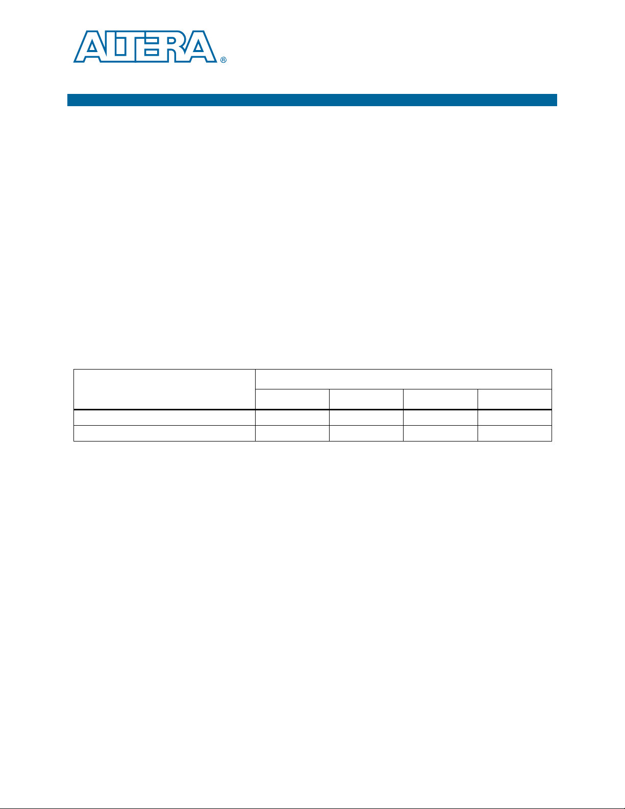
Figure 1–1 shows a PCI Express link between two Arria V FPGAs. One is configured
as a Root Port and the other as an Endpoint.
Figure 1–1. PCI Express Application with a Single Root Port and Endpoint
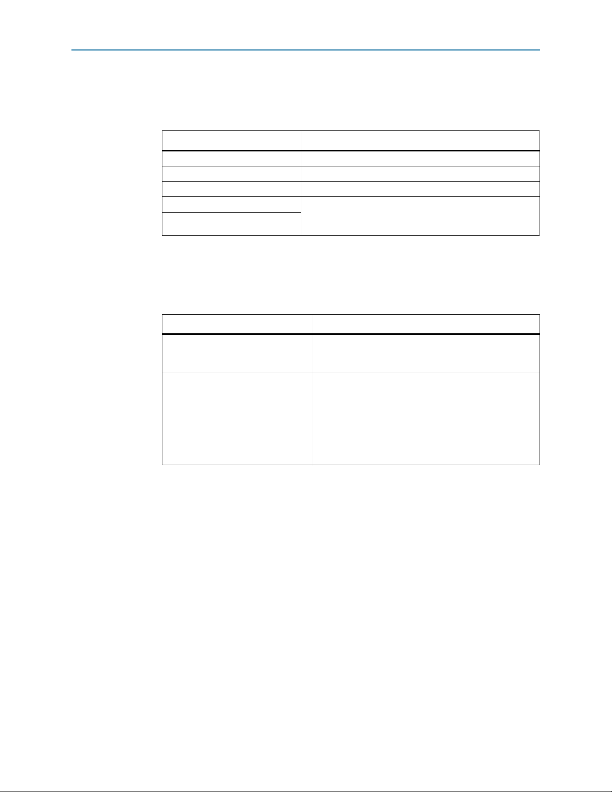
Figure 1–2 shows a PCI Express link between two Altera FPGAs. One is configured as
a Root Port and the other as a multi-function Endpoint. The FPGA serves as a custom
I/O hub for the host CPU. In the Arria V FPGA, each peripheral is treated as a
function with its own set of Configuration Space registers. Eight multiplexed
functions operate using a single PCI Express link.
Figure 1–2. PCI Express Application with an Endpoint Using the Multi-Function Capability
Debug Features
The Arria V Hard IP for PCI Express includes debug features that allow observation
and control of the Hard IP for faster debugging of system-level problems. For more
information about debugging refer to Chapter 19, C**Debugging.
December 2013 Altera Corporation Arria V Hard IP for PCI Express
User Guide
Page 14

1–6 Chapter 1: Datasheet
IP Core Verification
IP Core Verification
To ensure compliance with the PCI Express specification, Altera performs extensive
validation of the Arria V Hard IP Core for PCI Express. The Gen1 ×8 and Gen2 ×4
Endpoints were certified PCI Express compliant at PCI-SIG Compliance Workshop
#79 in February 2012.
The simulation environment uses multiple testbenches that consist of
industry-standard BFMs driving the PCI Express link interface. A custom BFM
connects to the application-side interface.
Altera performs the following tests in the simulation environment:
■ Directed and pseudo random stimuli areArria V applied to test the Application
Layer interface, Configuration Space, and all types and sizes of TLPs.
■ Error injection tests that inject errors in the link, TLPs, and Data Link Layer
Packets (DLLPs), and check for the proper responses
■ PCI-SIG
■ Random tests that test a wide range of traffic patterns
®
Compliance Checklist tests that specifically test the items in the checklist
Performance and Resource Utilization
Because the Arria V Hard IP for PCI Express IP core is implemented in hardened
logic, it uses less than 1% of Arria V resources. The Avalon-MM Arria V Hard IP for
PCI Express includes a bridge implemented in soft logic. Tab le 1 –4 shows the typical
expected device resource utilization for selected configurations of the Avalon-MM
Arria V Hard IP for PCI Express using the current version of the Quartus II software
targeting a Arria V (5AGXFB3H6F35C6ES) device. With the exception of M10K
memory blocks, the numbers of ALMs and logic registers in Table 1–4 are rounded up
to the nearest 100. Resource utilization numbers reflect changes to the resource
utilization reporting starting in the Quartus II software v12.1 release 28 nm device
families and upcoming device families.
f For information about Quartus II resource utilization reporting, refer to Fitter
Resources Reports in the Quartus II Help.
Table 1–5. Performance and Resource Utilization (Part 1 of 2)
ALMs Memory M10K Logic Registers
Avalon-MM Bridge
Gen1 ×4 1250 27 1700
Gen2 ×8 2100 35 3050
Avalon-MM Interface–Burst Capable Requester/Single DWord Completer
64 1150 23 1700
128 1600 29 2550
Avalon-MM Interface-Burst Capable Completer Only
64 600 11 900
128 1350 22 2300
Arria V Hard IP for PCI Express December 2013 Altera Corporation
User Guide
Page 15

Chapter 1: Datasheet 1–7
Recommended Speed Grades
Table 1–5. Performance and Resource Utilization (Part 2 of 2)
ALMs Memory M10K Logic Registers
Avalon-MM Interface–Completer Only
64 160 0 230
Soft calibration of the transceiver module requires additional logic. The amount of
logic required depends upon the configuration.
Recommended Speed Grades
Tab le 1 –5 lists the recommended speed grades for the supported link widths and
Application Layer clock frequencies. The speed grades listed are the only speed
grades that close timing. Altera recommends setting the Quartus II Analysis &
Synthesis Settings Optimization Technique to Speed.
h For information about optimizing synthesis, refer to “Setting Up and Running Analysis
and Synthesis in Quartus II Help.
For more information about how to effect the Optimization Technique settings, refer
to Area and Timing Optimization in volume 2 of the Quartus II Handbook.
Table 1–6. Device Family Link Width Application Frequency Recommended Speed Grades
Link Speed Link Width
×1 62.5
Application
Clock
Frequency (MHz)
(1)
–4, –5, –6
Recommended
Speed Grades
(2)
×1 125 –4, –5, –6
Gen1–2.5 Gbps
×2 125 –4, –5, –6
×4 125 –4, –5, –6
×8 125 –4, –5, –6
(1)
–4, –5,
Gen2–5.0 Gbps
×1 62.5
×1 125 –4, –5,,
×2 125 –4, –5,
×4 125 –4, –5,
Notes to Table 1–5:
(1) This is a power-saving mode of operation.
(2) Final results pending characterization by Altera. Refer to the fit.rpt file generated by the Quartus II software.
(2)
(2)
(2)
(2)
(2)
f For details on installation, refer to the Altera Software Installation and Licensing Manual.
December 2013 Altera Corporation Arria V Hard IP for PCI Express
User Guide
Page 16

1–8 Chapter 1: Datasheet
Recommended Speed Grades
Arria V Hard IP for PCI Express December 2013 Altera Corporation
User Guide
Page 17
2. Getting Started with the Arria Hard IP
APPS
altpcied_sv_hwtcl.v
Stratix V Hard IP for PCI Express Testbench for Endpoints
Avalon-ST TX
Avalon-ST RX
reset
status
Avalon-ST TX
Avalon-ST RX
reset
status
DUT
altpcie_sv_hip_ast_hwtcl.v
Root Port Model
altpcie_tbed_sv_hwtcl.v
PIPE or
Serial
Interface
Root Port BFM
altpcietb_bfm_rpvar_64b_x8_pipen1b
Root Port Driver and Monitor
altpcietb_bfm_vc_intf
December 2013
UG-01110-1.5
Getting Started with the Arria Hard IP for PCI Express
This section provides step-by-step instructions to help you quickly customize,
simulate, and compile the Arria Hard IP for PCI Express using either the
MegaWizard Plug-In Manager or Qsys design flow. When you install the Quartus II
software you also install the IP Library. This installation includes design examples for
Hard IP for PCI Express in <install_dir>/ip/altera/altera_pcie/
altera_pcie_hip_ast_ed/example_design/<device> directory.
1 If you have an existing Arria 12.1 or older design, you must regenerate it in 13.1
before compiling with the 13.1 version of the Quartus II software.
After you install the Quartus II software for 13.1, you can copy the design examples
from the <install_dir>/ip/altera/altera_pcie/altera_pcie_hip_ast_ed/
example_design/<device> directory. This walkthrough uses the Gen1 ×4 Endpoint.
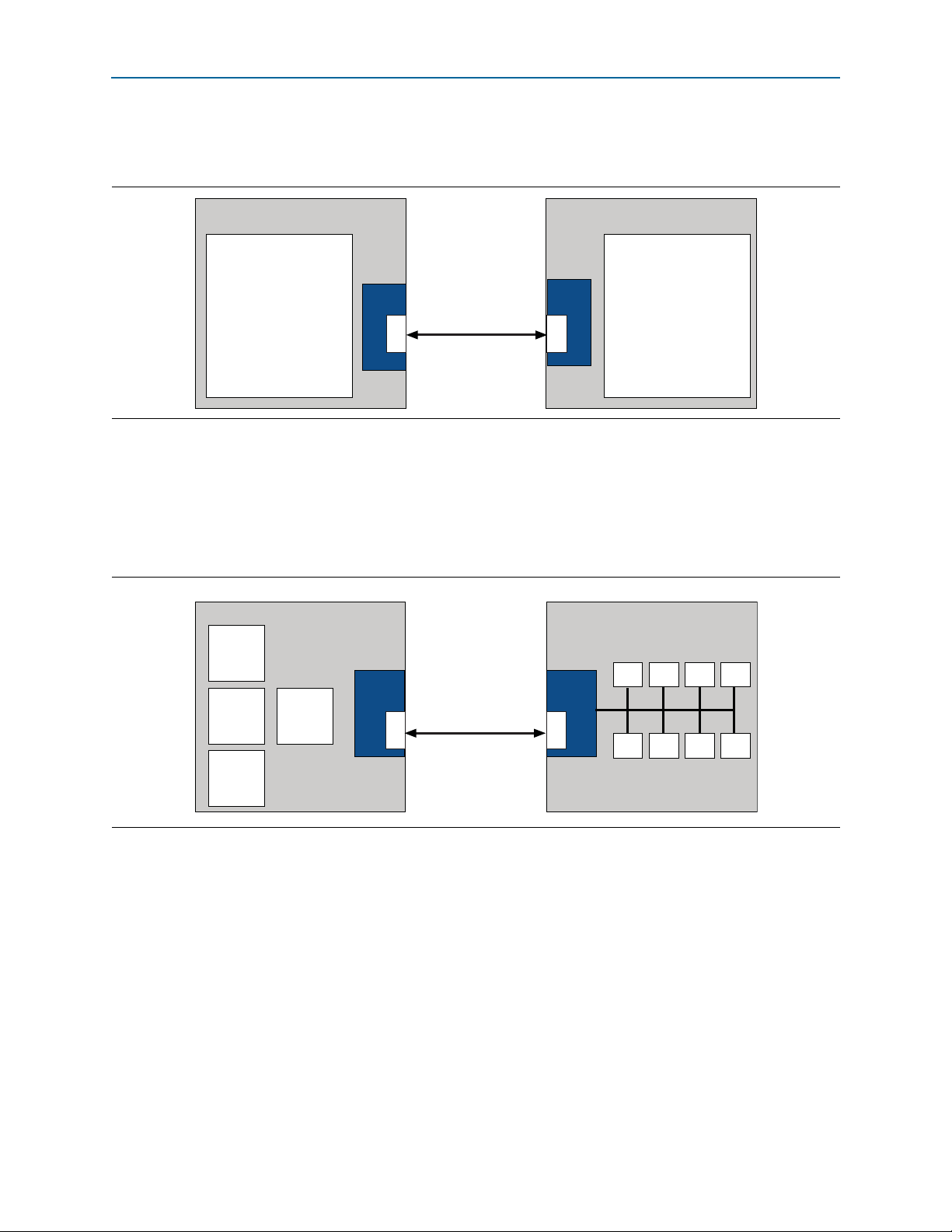
The following figure illustrates the top-level modules of the testbench in which the
DUT, a Gen1 ×4 Endpoint, connects to a chaining DMA engine, labeled APPS in the
following figure, and a Root Port model. The Transceiver Reconfiguration Controller
dynamically reconfigures analog settings to optimize signal quality of the serial
interface. The pcie_reconfig_driver drives the Transceiver Reconfiguration Controller.
The simulation can use the parallel PHY Interface for PCI Express (PIPE) or serial
interface.
for PCI Express
Figure 2–1. Testbench for an Endpoint
For a detailed explanation of this example design, refer to Chapter 18, Testbench and
December 2013 Altera Corporation Arria V Hard IP for PCI Express
Design Example. If you choose the parameters specified in this chapter, you can run
all of the tests included in Chapter 18.
L
User Guide
Page 18
2–2 Chapter 2: Getting Started with the Arria Hard IP for PCI Express
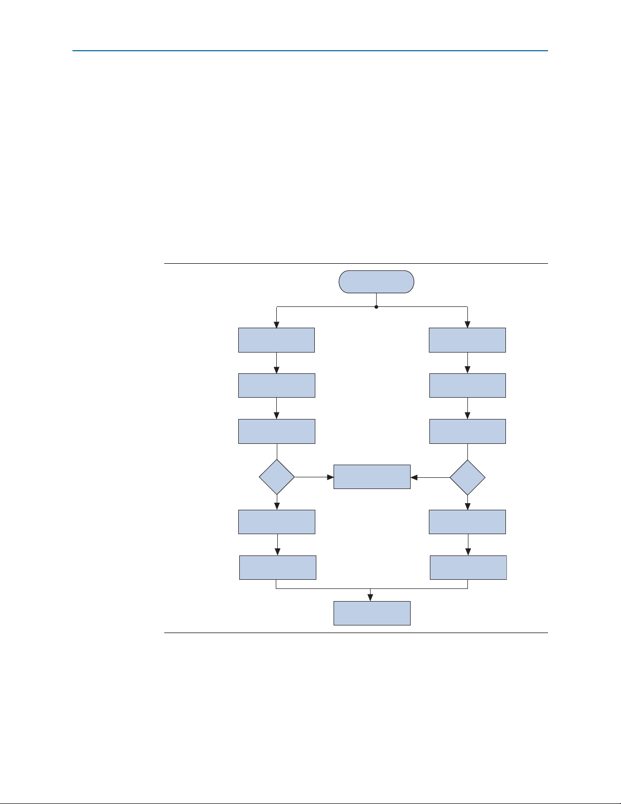
Select Design Flow
Customize the
Hard IP for PCIe
Qsys Flow
MegaWizard Plug-In
Manager Flow
Complete Qsys System
Run Simulation
Create Quartus II Project
Add Quartus IP File (.qip)
Create Quartus II Project
Generate the Simulation
Model for ModelSim, NC-Sim
or VCS
Generate the Simulation
Model in Qsys
Compile the Design for the
Qsys Design Flow
Modify Example Design
to Meet Your Requirements
Compile the Design for the
MegaWizard Design Flow
Add Quartus IP File (.qip)
to Quartus II Project
Customize the
Hard IP for PCIe
Step 1
Step 2
Step 3
Step 4
Step 5
Step 6
Step 7
Ye s
No
Simulating?
Ye s
No
Simulating?
Getting Started with the Arria Hard IP for PCI Express
The Arria Hard IP for PCI Express offers exactly the same feature set in both the
MegaWizard and Qsys design flows. Consequently, your choice of design flow
depends on whether you want to integrate the Arria Hard IP for PCI Express using
RTL instantiation or using Qsys, which is a system integration tool available in the
Quartus II software.
f For more information about Qsys, refer to System Design with Qsys in the Quartus II
Handbook.
h For more information about the Qsys GUI, refer to About Qsys in Quartus II Help.
The following figure illustrates the steps necessary to customize the Arria Hard IP for
PCI Express and run the example design.
Figure 2–2. MegaWizard Plug-In Manager and Qsys Design Flows
Arria V Hard IP for PCI Express December 2013 Altera Corporation
User Guide
Page 19

Chapter 2: Getting Started with the Arria Hard IP for PCI Express 2–3
MegaWizard Plug-In Manager Design Flow
MegaWizard Plug-In Manager Design Flow
This section guides you through the steps necessary to customize the Arria Hard IP
for PCI Express and run the example testbench, starting with the creation of a
Quartus II project.
Follow these steps to copy the example design files and create a Quartus II project.
1. Choose Programs > Altera > Quartus II <version> (Windows Start menu) to run
the Quartus II software.
2. On the Quartus II File menu, click New, then New Quartus II Project, then OK.
3. Click Next in the New Project Wizard: Introduction (The introduction does not
display if you previously turned it off.)
4. On the Directory, Name, Top-Level Entity page, enter the following information:
a. The working directory for your project. This design example uses
<working_dir>/example_design
b. The name of the project. This design example uses pcie_de_gen1_x4_ast64.
1 The Quartus II software specifies a top-level design entity that has the same
name as the project automatically. Do not change this name.
5. Click Next to display the Add Files page.
6. Click Yes, if prompted, to create a new directory.
7. Click Next to display the Family & Device Settings page.
8. On the Family & Device Settings page, choose the following target device family
and options:
a. In the Family list, select Arria V (/GX/GT/ST/SX)
b. In the Devices list, select Arria V GX Extended Features GX PCIe
c. In the Available devices list, select 5AGXFB3H6F35C6ES.
9. Click Next to close this page and display the EDA Tool Settings page.
10. From the Simulation list, select ModelSim
language you intend to use for simulation.
11. Click Next to display the Summary page.
12. Check the Summary page to ensure that you have entered all the information
correctly.
13. Click Finish to create the Quartus II project.
®
. From the Format list, select the HDL
Customizing the Endpoint in the MegaWizard Plug-In Manager Design Flow
This section guides you through the process of customizing the Endpoint in the
MegaWizard Plug-In Manager design flow. It specifies the same options that are
chosen in Chapter 18, Testbench and Design Example.
Follow these steps to customize your variant in the MegaWizard Plug-In Manager:
December 2013 Altera Corporation Arria V Hard IP for PCI Express
User Guide
Page 20

2–4 Chapter 2: Getting Started with the Arria Hard IP for PCI Express
Customizing the Endpoint in the MegaWizard Plug-In Manager Design Flow
1. On the Tools menu, click MegaWizard Plug-In Manager. The MegaWizard
Plug-In Manager appears.
2. Select Create a new custom megafunction variation and click Next.
3. In Which device family will you be using? Select the Arria device family.
4. Expand the Interfaces directory under Installed Plug-Ins by clicking the + icon
left of the directory name, expand PCI Express, then click Arria Hard IP for PCI
Express <version_number>
5. Select the output file type for your design. This walkthrough supports VHDL and
Verilog HDL. For this example, select Verilog HDL.
6. Specify a variation name for output files <working_dir>/example_design/
<variation name>. For this walkthrough, specify <working_dir>/example_design/
gen1_x4.
7. Click Next to open the parameter editor for the Arria Hard IP for PCI Express.
8. Specify the System Settings values listed in the following table.
Table 2–1. System Settings Parameters
Parameter Value
Number of Lanes x4
Lane Rate Gen 1 (2.5 Gbps)
Port type Native endpoint
Application Layer interface Avalon-ST 64-bit
RX buffer credit allocation - performance for
received requests
Reference clock frequency 100 MHz
Use 62.5 MHz Application Layer clock for ×1 Leave this option off
Use deprecated RX Avalon-ST data byte enable
port (rx_st_be)
Enable configuration via the PCIe link Leave this option off
Number of functions 1
Low
Leave this option off
1 Each function shares the parameter settings on the Device, Error Reporting, Link,
Slot, and Power Management tabs. Each function has separate parameter settings for
the Base Address Registers, Base and Limit Registers for Root Ports, Device
Identification Registers, and the PCI Express/PCI Capabilities parameters. When
you click on a Func<n> tab under the Port Functions heading, the tabs automatically
reflect the Func<n> tab selected.
9. Specify the Device parameters listed in Ta bl e 2– 2.
Table 2–2. Device
Parameter Value
Maximum payload size 128 bytes
Number of tags supported 32
Completion timeout range ABCD
Implement completion timeout disable On
Arria V Hard IP for PCI Express December 2013 Altera Corporation
User Guide
Page 21
Chapter 2: Getting Started with the Arria Hard IP for PCI Express 2–5
Customizing the Endpoint in the MegaWizard Plug-In Manager Design Flow
10. On the Error Reporting tab, leave all options off.
11. Specify the Link settings listed in Tab le 2 –7 .
Table 2–3. Link Tab
Parameter Value
Link port number 1
Slot clock configuration On
12. On the Slot Capabilities tab, leave the Slot register turned off.
13. Specify the Power Management parameters listed in Ta bl e 2–4 .
Table 2–4. Power Management Parameters
Parameter Value
Endpoint L0s acceptable exit latency Maximum of 64 ns
Endpoint L1 acceptable latency Maximum of 1 µs
14. Specify the BAR settings for Func0 listed in Ta bl e 2– 5.
Table 2–5. Base Address Registers for Func0
Parameter Value
BAR0 Type 64-bit prefetchable memory
BAR0 Size 256 MBytes - 28 bits
BAR1 Type Disabled
BAR1 Size N/A
BAR2 Type 32-bit non-prefetchable memory
BAR2 Size 1 KByte - 10 bits
15. You can leave Func0 BAR3 through Func
16. 0 BAR5 and the Func0 Expansion ROM Disabled.
17. Under the Base and Limit Registers heading, disable both the Input/Output and
Prefetchable memory options. (These options are for Root Ports.)
18. For the Device ID Registers for Func0, specify the values listed in the center
column of Table 2–6. The right-hand column of this table lists the value assigned to
Altera devices. You must use the Altera values to run the reference design
described in AN 456 PCI Express High Performance Reference Design. Be sure to use
your company’s values for your final product.
Table 2–6. Device ID Registers for Func0
Register Name Value Altera Value
Vendor ID
Device ID
Revision ID
Class Code
0x00000000
0x00000001
0x00000001
0x00000000
0x00001172
0x0000E001
0x00000001
0x00FF0000
December 2013 Altera Corporation Arria V Hard IP for PCI Express
User Guide
Page 22
2–6 Chapter 2: Getting Started with the Arria Hard IP for PCI Express
Table 2–6. Device ID Registers for Func0
Subsystem Vendor ID
Subsystem Device ID
Customizing the Endpoint in the MegaWizard Plug-In Manager Design Flow
0x00000000
0x00000000
0x00001172
0x0000E001
19. On the Func 0 Device tab, under PCI Express/PCI Capabilities for Func 0 turn
Function Level Reset (FLR) Off.
20. Ta bl e 2 –7 lists settings for the Func0 Link tab.
Table 2–7. Link Capabilities
Parameter Value
Data link layer active reporting Off
Surprise down reporting Off
21. On the Func0 MSI tab, for Number of MSI messages requested, select 4.
22. On the Func0 MSI-X tab, turn Implement MSI-X off.
23. On the Func0 Legacy Interrupt tab, select INTA.
24. the following tablethe following tablethe following tablethe following tablethe
following tablethe following tableClick Finish. The Generation dialog box
appears.
25. Turn on Generate Example Design to generate the Endpoint, testbench, and
supporting files.
26. Click Exit.
27. Click Yes if you are prompted to add the Quartus II IP File (.qip) to the project.
The .qip is a file generated by the parameter editor contains all of the necessary
assignments and information required to process the IP core in the Quartus II
compiler. Generally, a single .qip file is generated for each IP core.
Understanding the Files Generated
The following table provides an overview of directories and files generated.
Table 2–8. Qsys Generation Output Files
Directory Description
<working_dir>/<variant_name>/ Includes the files for synthesis
<working_dir>/<variant_name>_sim/
altera_pcie_<device>_hip_ast
<working_dir>/<variant_name>_example_design/
altera_pcie_<device>_hip_ast
Includes the simulation files.
Includes a Qsys testbench that connects the Endpoint to a chaining
DMA engine, Transceiver Reconfiguration Controller, and driver for the
Transceiver Reconfiguration Controller.
Follow these steps to generate the chaining DMA testbench from the Qsys system
design example.
1. On the Quartus II File menu, click Open.
2. Navigate to the Qsys system in the altera_pcie_<device>_hip_ast subdirectory.
Arria V Hard IP for PCI Express December 2013 Altera Corporation
User Guide
Page 23
Chapter 2: Getting Started with the Arria Hard IP for PCI Express 2–7
Customizing the Endpoint in the MegaWizard Plug-In Manager Design Flow
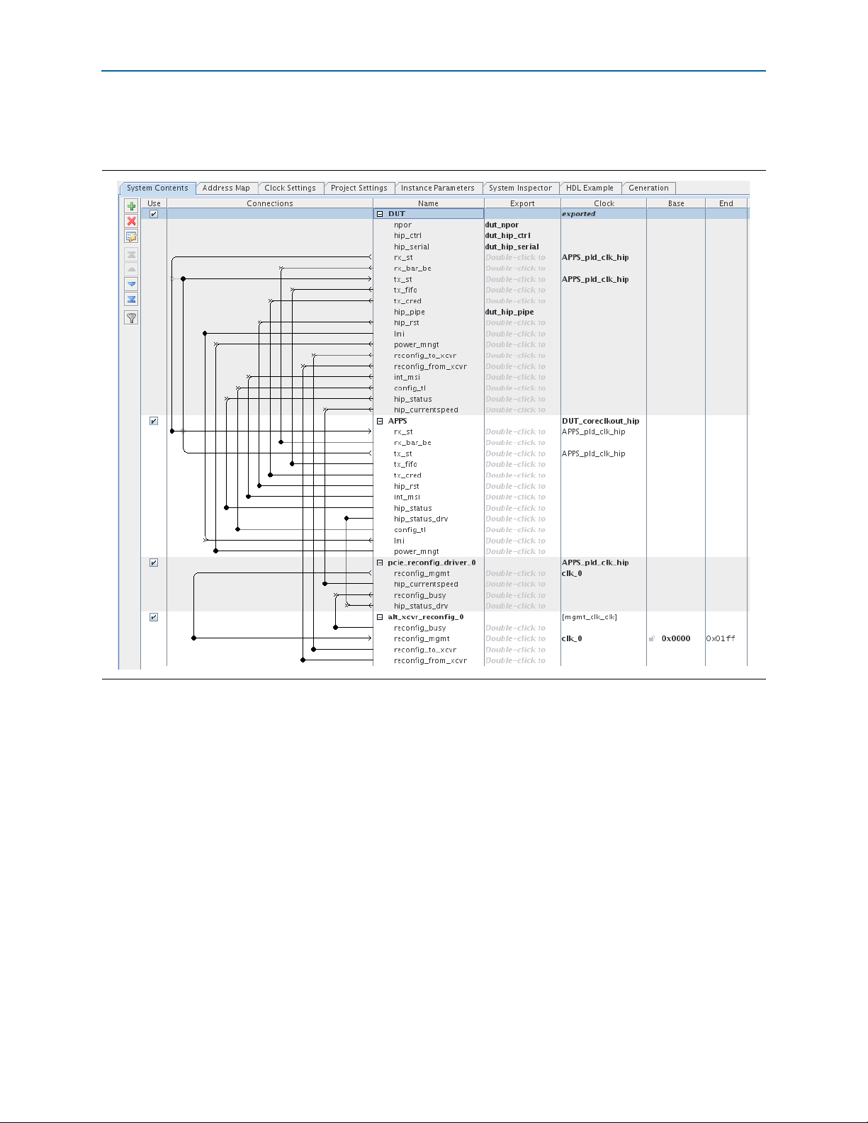
3. Click pcie_de_gen1_x4_ast64.qsys to bring up the Qsys design. The following
figure illustrates this Qsys system.
Figure 2–3. Qsys System Connecting the Endpoint Variant and Chaining DMA Testbench
December 2013 Altera Corporation Arria V Hard IP for PCI Express
User Guide
Page 24
2–8 Chapter 2: Getting Started with the Arria Hard IP for PCI Express
Customizing the Endpoint in the MegaWizard Plug-In Manager Design Flow
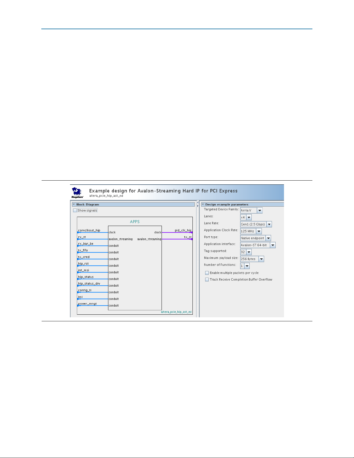
4. To display the parameters of the APPS component shown in the previous figure,
click on it and then select Edit from the right-mouse menuFigure 2–4. illustrates
this component. Note that the values for the following parameters match those set
in the DUT component:
■ Targeted Device Family
■ Lanes
■ Lane Rate
■ Application Clock Rate
■ Port
■ Application interface
■ Tags supported
■ Maximum payload size
■ Number of Functions
Figure 2–4. Qsys Component Representing the Chaining DMA Design Example
1 You can use this Qsys APPS component to test any Endpoint variant with
compatible values for these parameters.
5. To close the APPS component, click the X in the upper right-hand corner of the
parameter editor.
Go to “Simulating the Example Design ###avst_sim###” on page 2–11 for instructions
on system simulation.
Arria V Hard IP for PCI Express December 2013 Altera Corporation
User Guide
Page 25
Chapter 2: Getting Started with the Arria Hard IP for PCI Express 2–9
Qsys Design Flow
Qsys Design Flow
This section guides you through the steps necessary to customize the Arria Hard IP
for PCI Express and run the example testbench in Qsys. Reviewing the Qsys Example
Design for PCIe
For this example, copy the Gen1 x4 Endpoint example design from installation
directory: <install_dir>/ip/altera/altera_pcie/altera_pcie_hip_ast_ed/example_design
/<device> directory to a working directory.
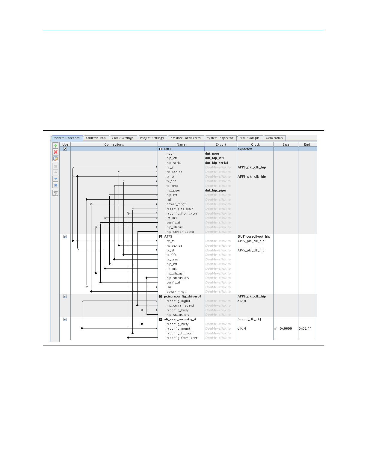
The following figure illustrates this Qsys system.
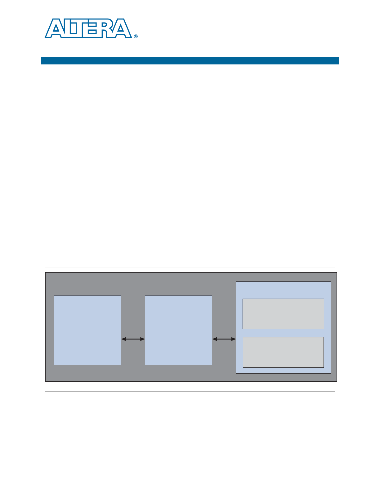
Figure 2–5. Complete Gen1 ×4 Endpoint (DUT) Connected to Example Design (APPS)
The example design includes the following four components:
■ DUT—This is Gen1 x4 Endpoint. For your own design, you can select the data
rate, number of lanes, and either Endpoint or Root Port mode.
■ APPS—This Root Port BFM configures the DUT and drives read and write TLPs to
test DUT functionality. An Endpoint BFM is available if your PCI Express design
implements a Root Port.
December 2013 Altera Corporation Arria V Hard IP for PCI Express
User Guide
Page 26

2–10 Chapter 2: Getting Started with the Arria Hard IP for PCI Express
■ pcie_reconfig_driver_0—This Avalon-MM master drives the Transceiver
Qsys Design Flow
Reconfiguration Controller. The pcie_reconfig_driver_0 is implemented in clear
text that you can modify if your design requires different reconfiguration
functions. After you generate your Qsys system, the Verilog HDL for this
component is available as: <working_dir>/<variant_name>/testbench/
<variant_name>_tb/simulation/submodules/altpcie_reconfig_driver.sv.
■ Transceiver Reconfiguration Controller—The Transceiver Reconfiguration
Controller dynamically reconfigures analog settings to improve signal quality. For
Gen1 and Gen2 data rates, the Transceiver Reconfiguration Controller must
perform offset cancellation and PLL calibration.
Generating the Testbench
Follow these steps to generate the chaining DMA testbench:
1. On the Qsys Generation tab, specify the parameters listed in the following table.
Table 2–9. Parameters to Specify on the Generation Tab in Qsys
Parameter Value
Simulation
Create simulation model
None. (This option generates a simulation model you can include in your own
custom testbench.)
Create testbench Qsys system Standard, BFMs for standard Avalon interfaces
Create testbench simulation model Verilog
Synthesis
Create HDL design files for synthesis Turn this option on
Create block symbol file (.bsf) Turn this option on
Output Directory
Path pcie_qsys/gen1_x4_example_design
Simulation Leave this option blank
Testbench
Synthesis
Note to Table 2–9:
(1) Qsys automatically creates this path by appending testbench to the output directory/.
(2) Qsys automatically creates this path by appending synthesis to the output directory/.
(1)
(2)
pcie_qsys/gen1_x4_example_design/testbench
pcie_qsys/gen1_x4_example_design/synthesis
2. Click the Generate button at the bottom of the Generation tab to create the
chaining DMA testbench.
Arria V Hard IP for PCI Express December 2013 Altera Corporation
User Guide
Page 27

Chapter 2: Getting Started with the Arria Hard IP for PCI Express 2–11
Qsys Design Flow
Understanding the Files Generated
The following table provides an overview of the files and directories Qsys generates.
Table 2–10. Qsys Generation Output Files
Directory Description
includes the top-level HDL file for the Hard I for PCI Express and the .qip file that
<testbench_dir>/<variant_name>/
synthesis
<testbench_dir>/<variant_name>/
synthesis/submodules
<testbench_dir>/<variant_name>/
testbench/
<testbench_dir>/<variant_name>/
testbench/<cad_vendor>
lists all of the necessary assignments and information required to process the IP
core in the Quartus II compiler. Generally, a single .qip file is generated for each IP
core.
Includes the HDL files necessary for Quartus II synthesis.
Includes testbench subdirectories for the Aldec, Cadence and Mentor simulation
tools with the required libraries and simulation scripts.
Includes the HDL source files and scripts for the simulation testbench.
Simulating the Example Design
Follow these steps to compile the testbench for simulation and run the chaining DMA
testbench.
1. Start your simulation tool. This example uses the ModelSim
®
software.
2. From the ModelSim transcript window, in the testbench directory
(./example_design/altera_pcie_<device>_hip_ast/<variant>/testbench/mentor)
type the following commands:
a.
do msim_setup.tcl
r
b. h r (This is the ModelSim help command.)
c. ld_debug r (This command compiles all design files and elaborates the
top-level design without any optimization.)
d. run -all r
The following example shows a partial transcript from a successful simulation. As this
transcript illustrates, the simulation includes the following stages:
■ Link training
■ Configuration
■ DMA reads and writes
December 2013 Altera Corporation Arria V Hard IP for PCI Express
User Guide
Page 28

2–12 Chapter 2: Getting Started with the Arria Hard IP for PCI Express
■ Root Port to Endpoint memory reads and writes
Qsys Design Flow
Example 2–1. Excerpts from Transcript of Successful Simulation Run
Time: 56000 Instance: top_chaining_testbench.ep.epmap.pll_250mhz_to_500mhz.
# Time: 0 Instance:
pcie_de_gen1_x8_ast128_tb.dut_pcie_tb.genblk1.genblk1.altpcietb_bfm_top_rp.rp.rp.nl00O
0i.Arria ii_pll.pll1
# Note : Arria II PLL locked to incoming clock
# Time: 25000000 Instance:
pcie_de_gen1_x8_ast128_tb.dut_pcie_tb.genblk1.genblk1.altpcietb_bfm_top_rp.rp.rp.nl00O
0i.Arria ii_pll.pll1
# INFO: 464 ns Completed initial configuration of Root Port.
# INFO: 3661 ns RP LTSSM State: DETECT.ACTIVE
# I
NFO: 3693 ns RP LTSSM State: POLLING.ACTIVE
# INFO:
# I
# I
# I
# INFO: 7
# INFO: 7969 ns EP LTS
3905 ns EP LTSSM State: DETECT.ACTIVE
NFO: 4065 ns EP LTSSM State: POLLING.ACTIVE
NFO: 6369 ns EP LTSSM State: POLLING.CONFIG
NFO: 6461 ns RP LTSSM State: POLLING.CONFIG
741 ns RP LTSSM State: CONFIG.LINKWIDTH.START
SM State: CONFIG.LINKWIDTH.START
# INFO: 8353 ns EP LTSSM State: CONFIG.LINKWIDTH.ACCEPT
NFO: 8781 ns RP LTSSM State: CONFIG.LINKWIDTH.ACCEPT
# I
# INFO: 9537 ns EP LTSSM State: CONFIG.LANENUM.WAIT
# INFO:
# INFO:
# INFO: 10189 ns RP LTSSM State: CO
9857 ns EP LTSSM State: CONFIG.LANENUM.ACCEPT
9933 ns RP LTSSM State: CONFIG.LANENUM.ACCEPT
NFIG.COMPLETE
# INFO: 10689 ns EP LTSSM State: CONFIG.COMPLETE
# INFO: 121
# INFO: 136
# INFO:
13889 ns EP LTSSM State: L0
09 ns RP LTSSM State: CONFIG.IDLE
97 ns EP LTSSM State: CONFIG.IDLE
# INFO: 13981 ns RP LTSSM State: L0
# INFO: 17800 ns Configuring Bus 001, Device 001, Function 00
# INFO:
17800 ns EP Read Only Configuration Registers:
# INFO: 17800 ns Vendor ID: 1172
# INFO: 17800 ns Device ID: E001
# INFO: 17800 ns Revision ID: 01
# INFO: 17800 ns Class Code: FF0000
# INFO: 17800 ns Subs
ystem Vendor ID: 1172
# INFO: 17800 ns Subsystem ID: E001
# INFO: 17800 ns Interrupt Pin: INTA# used
# INFO: 17800 ns
# INFO: 20040 ns PCI MSI Capability Register:
FO: 20040 ns 64-Bit Address Capable: Supported
# IN
# I
NFO: 20040 ns Messages Requested: 4
# INFO
: 20040 ns
#INFO: 31208 ns EP PCI Express Link Status Register (1081):
# INFO: 31208 ns Negotiated Link Width: x8
# INF
O: 31208 ns Slot Clock Config: System Reference Clock Used
# INFO: 33481 ns RP LTSSM State: RECOVERY.RCVRLOCK
# IN
FO: 34321 ns EP LTSSM State: RECOVERY.RCVRLOCK
# INFO: 3
# INFO: 3
# I
NFO: 36377 ns RP LTSSM State: RECOVERY.IDLE
# I
NFO: 37457 ns EP LTSSM State: RECOVERY.IDLE
4961 ns EP LTSSM State: RECOVERY.RCVRCFG
5161 ns RP LTSSM State: RECOVERY.RCVRCFG
# INFO: 37649 ns EP LTSSM State: L0
# INFO: 37737 ns RP LTSSM State: L0
# INFO: 399
44 ns Current Link Speed: 2.5GT/s
# INFO: 58904 ns Completed configuration of Endpoint BARs.
INFO: 61288 ns ---------
#
# INFO: 61288 ns TASK:chained_dma_test
# I
NFO: 61288 ns DMA: Read
Arria V Hard IP for PCI Express December 2013 Altera Corporation
User Guide
Page 29

Chapter 2: Getting Started with the Arria Hard IP for PCI Express 2–13
Qsys Design Flow
Example 2–1. Excerpts from Transcript of Successful Simulation Run (continued)
# INFO: 8973 ns RP LTSSM State: CONFIG.LANENUM.WAIT
# INFO: 61288 ns ---------
# INFO: 61288 ns TASK:dma_rd_test
# INFO: 61288 ns ---------
# INFO: 61288 ns TASK:dma_set_rd_desc_data
#
INFO: 61288 ns ---------
# INFO: 61288 ns TASK:dma_set_msi READ
# INFO: 61288 ns Message Signaled Interrupt Configuration
# IN
FO: 61288 ns msi_address (RC memory)= 0x07F0
# INFO:
# I
# IN
63512 ns msi_control_register = 0x0084
NFO: 72440 ns msi_expected = 0xB0FC
FO: 72440 ns msi_capabilities address = 0x0050
# INFO: 72440 ns multi_message_enable = 0x0002
# INFO: 72440 ns msi_number = 0000
# INFO: 72440 ns msi_traffic_class = 0000
# INFO: 72440 ns ---------
# INFO: 72440 ns TASK:dma_set_header READ
# INFO: 72440 ns Writing Descriptor header
# INFO: 724
# INFO
: 72480 ns
80 ns data content of the DT header
# INFO: 72480 ns Shared Memory Data Display:
# INFO: 72480 ns Address Data
# INFO: 72480 ns ------- ----
# INFO: 72480 ns 00000900 00000003 00000000 00000900 CAFEFADE
#
INFO: 72480 ns ---------
# INFO: 72480 ns TASK:dma_set_rclast
# IN
FO: 72480 ns Start READ DMA : RC issues MWr (RCLast=0002)
# INFO: 72496 ns ---------
# INFO: 72509 ns TASK:msi_poll Po
lling MSI Address:07F0---> Data:FADE......
# INFO: 72693 ns TASK:rcmem_poll Polling RC Address0000090C current data
(0000FADE) expected data (00000002)
# INFO: 80693 ns TASK:rcmem_poll Polling RC Address0000090C current data
(00000000) expected data (00000002)
# INFO: 84749 ns TASK:msi_poll Received DMA Read MSI(0000) : B0FC
# I
NFO: 84893 ns TASK:rcmem_poll Polling RC Address0000090C current data
(00000002) expected data (00000002)
# INFO: 84893 ns TASK:rcmem_poll ---> Received Expected Data (00000002)
# INFO: 84901 ns --------# INFO: 84901 ns Completed DMA Read
# INFO: 84901 ns TASK:chained_dma_test
# INFO: 84901 ns DMA: Write
# INFO: 84901 ns ---------
# INFO: 84901 ns TASK:dma_wr_test
# INFO: 84901 ns DMA: Write
# INFO: 84901 ns ---------
# INFO: 84901 ns TASK:dm
a_set_wr_desc_data
# INFO: 84901 ns ---------
# INFO: 84901 ns TASK:dma_set_msi WRITE
# IN
FO: 84901 ns Message Signaled Interrupt Configuration
FO: 84901 ns msi_address (RC memory)= 0x07F0
# IN
# INFO:
# I
# I
87109 ns msi_control_register = 0x00A5
NFO: 96005 ns msi_expected = 0xB0FD
NFO: 96005 ns msi_capabilities address = 0x0050
December 2013 Altera Corporation Arria V Hard IP for PCI Express
User Guide
Page 30

2–14 Chapter 2: Getting Started with the Arria Hard IP for PCI Express
Qsys Design Flow
Example 2-1Excerpts from Transcript of Successful Simulation Run (continued)
# INFO: 96005 ns multi_message_enable = 0x0002
# INFO: 96005 ns msi_number = 0001
# INFO: 96005 ns msi_tr
# INFO: 96005 ns ---------
# INFO: 96005 ns TASK:dma_set_header WRITE
# INFO
# INFO: 960
# INFO
# INFO: 96045 ns Shared Memory Data Display:
# INFO: 96045 ns Address Data
# INFO: 96045 ns ------- ----
# INFO: 96045 ns 00000800 10100003 00000000 00000800 CAFEFADE
#
# INFO: 96045 ns TASK:dma_set_rclast
# INFO: 96045 ns Start WRITE DMA : RC issues MWr (RCLast=0002)
# INFO: 96061 ns ---------
# INFO: 96073 ns TASK:msi_poll Po
# INFO: 96257 ns TASK:rcmem_poll Polling RC Address0000080C current data
(0000FADE) expected data (00000002)
# INFO: 101457 ns TASK:rcmem_poll Polling RC Address0000080C current data
(00000000) expected data (00000002)
# INFO: 105177 ns TASK:msi_poll Received DMA Write MSI(0000) : B0FD
# I
(00000002) expected data (00000002)
# INFO: 105257 ns TASK:rcmem_poll ---> Received Expected Data (00000002)
# INFO: 105265 ns ---------
# INFO: 105265 ns Completed DMA Write
# INFO
# INFO: 105265 ns TASK:check_dma_data
# INFO: 105265 ns Passed : 0644 identical dwords.
# INFO
# INFO: 105265 ns TASK:downstream_loop
# INFO: 107897 ns Passed: 0004 same bytes in BFM mem addr 0x00000040 and 0x00000840
# INFO: 110409 ns Passed: 0008 same bytes in BFM mem addr 0x00000040 and 0x00000840
# INFO: 113
# INFO: 115665 ns Passed: 0016 same bytes in BFM mem addr 0x00000040 and 0x00000840
# INFO: 118305 ns Passed: 0020 same bytes in BFM mem addr 0x00000040 and 0x00000840
# INFO: 120
# INFO: 123577 ns Passed: 0028 same bytes in BFM mem addr 0x00000040 and 0x00000840
# INFO: 126
# INFO: 128897 ns Passed: 0036 same bytes in BFM mem addr 0x00000040 and 0x00000840
# INFO: 131545 ns Passed: 0040 same bytes in BFM mem addr 0x00000040 and 0x00000840
# SUCCESS: Simulation stopped due to successful completion!
: 96005 ns Writing Descriptor header
45 ns data content of the DT header
: 96045 ns
INFO: 96045 ns ---------
NFO: 105257 ns TASK:rcmem_poll Polling RC Address0000080C current data
: 105265 ns ---------
: 105265 ns ---------
033 ns Passed: 0012 same bytes in BFM mem addr 0x00000040 and 0x00000840
937 ns Passed: 0024 same bytes in BFM mem addr 0x00000040 and 0x00000840
241 ns Passed: 0032 same bytes in BFM mem addr 0x00000040 and 0x00000840
affic_class = 0000
lling MSI Address:07F0---> Data:FADE......
Understanding Channel Placement Guidelines
Arria transceivers are organized in banks of three and six channels for 6-Gbps
operation and in banks of two channels for 10-Gbps operation. The transceiver bank
boundaries are important for clocking resources, bonding channels, and fitting. Refer
to “Channel Placement Using CMU PLL” on page 7–50, “Channel Placement for ×4
Variants” on page 7–48, and “Channel Placement for ×8 Variants” on page 7–49 for
information about channel placement.
f For more information about Arria transceivers refer to the “Transceiver Banks”
section in the Transceiver Architecture in Arria V Devices.
Arria V Hard IP for PCI Express December 2013 Altera Corporation
User Guide
Page 31

Chapter 2: Getting Started with the Arria Hard IP for PCI Express 2–15
Compiling the Design in the Qsys Design Flow
Compiling the Design in the MegaWizard Plug-In Manager Design Flow
Before compiling the complete example design in the Quartus II software, you must
add the example design files that you generated in Qsys to your Quartus II project.
The Quartus II IP File (.qip) lists all files necessary to compile the project.
Follow these steps to add the Quartus II IP File (.qip) to the project:
1. On the Project menu, select Add/Remove Files in Project.
2. Click the browse button next the File name box and browse to the
gen1_x4_example_design/altera_pcie_sv_hip_ast/pcie_de_gen1_x4_ast64/
synthesis/ directory.
3. In the Files of type list, Click pcie_de_ge1_x4_ast64.qip and then click Open.
4. On the Add Files page, click Add, then click OK.
5. Add the Synopsys Design Constraints (SDC) shown in the following example, to
the top-level design file for your Quartus II project.
Example 2–2. Synopsys Design Constraint
create_clock -period “100 MHz” -name {refclk_pci_express} {*refclk_*}
derive_pll_clocks
derive_clock_uncertainty
######################################################################
# PHY IP reconfig controller constraints
# Set reconfig_xcvr clock
# Modify to match the actual clock pin name
# used for this clock, and also changed to have the correct period set
create_clock -period "125 MHz" -name {reconfig_xcvr_clk}
{*reconfig_xcvr_clk*}
######################################################################
# HIP Soft reset controller SDC constraints
set_false_path -to [get_registers
*altpcie_rs_serdes|fifo_err_sync_r[0]]
set_false_path -from [get_registers *sv_xcvr_pipe_native*] -to
[get_registers *altpcie_rs_serdes|*]
# Hard IP testin pins SDC constraints
set_false_path -from [get_pins -compatibilitly_mode *hip_ctrl*]
6. On the Processing menu, select Start Compilation.
Compiling the Design in the Qsys Design Flow
To compile the Qsys design example in the Quartus II software, you must create a
Quartus II project and add your Qsys files to that project.
Complete the following steps to create your Quartus II project:
1. From the Windows Start Menu, choose Programs > Altera > Quartus II 13.1 to run
the Quartus II software.
December 2013 Altera Corporation Arria V Hard IP for PCI Express
User Guide
Page 32

2–16 Chapter 2: Getting Started with the Arria Hard IP for PCI Express
Compiling the Design in the Qsys Design Flow
2. Click the browse button next the File name box and browse to the
gen1_x4_example_design/altera_pcie_<dev>_ip_ast/pcie_de_gen1_x4_ast64/
synthesis/ directory.
3. On the Quartus II File menu, click New, then New Quartus II Project, then OK.
4. Click Next in the New Project Wizard: Introduction (The introduction does not
appear if you previously turned it off.)
5. On the Directory, Name, Top-Level Entity page, enter the following information:
a. The working directory shown is correct. You do not have to change it.
b. For the project name, click the browse buttons and select your variant name,
pcie_de_gen1_x4_ast64 then click Open.r
1 If the top-level design entity and Qsys system names are identical, the
Quartus II software treats the Qsys system as the top-level design entity.
6. Click Next to display the Add Files page.
7. Complete the following steps to add the Quartus II IP File (.qip) to the project:
a. Click the browse button. The Select File dialog box appears.
b. In the Files of type list, select IP Variation Files (*.qip).
c. Click pcie_de_gen1_x4_ast64.qip and then click Open.
d. On the Add Files page, click Add, then click OK.
8. Click Next to display the Device page.
9. On the Family & Device Settings page, choose the following target device family
and options:
a. In the Family list, select Arria V (GT/GX/ST/SX)
b. In the Devices list, select Arria V GX Extended Features GX PCIe
c. In the Available devices list, select 5AGXFB3H6F35C6ES.
10. Click Next to close this page and display the EDA Tool Settings page.
11. Click Next to display the Summary page.
12. Check the Summary
corr
ectly.
page to ensure that you have entered all the information
13. Click Finish to create the Quartus II project.
Arria V Hard IP for PCI Express December 2013 Altera Corporation
User Guide
Page 33

Chapter 2: Getting Started with the Arria Hard IP for PCI Express 2–17
Compiling the Design in the Qsys Design Flow
14. Add the Synopsys Design Constraint (SDC) shown inExample 2–3, to the top-level
design file for your Quartus II project.
Example 2–3. Synopsys Design Constraint
create_clock -period “100 MHz” -name {refclk_pci_express} {*refclk_*}
derive_pll_clocks
derive_clock_uncertainty
######################################################################
# PHY IP reconfig controller constraints
# Set reconfig_xcvr clock
# Modify to match the actual clock pin name
# used for this clock, and also changed to have the correct period set
create_clock -period "125 MHz" -name {reconfig_xcvr_clk}
{*reconfig_xcvr_clk*}
######################################################################
# HIP Soft reset controller SDC constraints
set_false_path -to [get_registers
*altpcie_rs_serdes|fifo_err_sync_r[0]]
set_false_path -from [get_registers *sv_xcvr_pipe_native*] -to
[get_registers *altpcie_rs_serdes|*]
# Hard IP testin pins SDC constraints
set_false_path -from [get_pins -compatibilitly_mode *hip_ctrl*]
15. To compile your design using the Quartus II software, on the Processing menu,
click Start Compilation. The Quartus II software then performs all the steps
necessary to compile your design.
December 2013 Altera Corporation Arria V Hard IP for PCI Express
User Guide
Page 34

PCB
Avalon-MM slave
Reset
Stratix V Hard IP for PCI Express
Stratix V FPGA
PCB
Transaction Layer
Data Link Layer
PHY MAC Layer
x8 PCIe Link
(Physical Layer)
Lane 7
(Unused)
(Unused)
Lane 6
Lane 5
TX PLL
PHY IP Core for PCI Express
Lane 2
Lane 3
Lane 4
Lane 1
Lane 0
TX PLL
Transceiver Bank
Transceiver Bank
S
Reconfig
to and from
Transceiver
to and from
Embedded
Controller
(Avalon-MM
slave interface)
Transceiver
Reconfiguration
Controller
Root
Port
BFM
npor
Reset
APPS DUT
Chaining DMA
(User Application)
2–18 Chapter 2: Getting Started with the Arria Hard IP for PCI Express
Modifying the Example Design
Modifying the Example Design
To use this example design as the basis of your own design, replace the Chaining
DMA Example shown in Figure 2–6 with your own Application Layer design. Then
modify the Root Port BFM driver to generate the transactions needed to test your
Application Layer.
.
Figure 2–6. Testbench for PCI Express
Arria V Hard IP for PCI Express December 2013 Altera Corporation
User Guide
Page 35

December 2013
UG-01110-1.5
3. Getting Started with the Avalon-MM Arria Hard IP for PCI Express
This Qsys design example provides detailed step-by-step instructions to generate a
Qsys system. When you install the Quartus II software you also install the IP Library.
This installation includes design examples for the Avalon-MM Arria Hard IP for PCI
Express in the <install_dir>/ip/altera/altera_pcie/altera_pcie_av_hip_avmm/
example_designs/ directory.
The design examples contain the following components:
■ Avalon-MM Arria Hard IP for PCI Express ×4 IP core
■ On-Chip memory
■ DMA controller
■ Transceiver Reconfiguration Controller
In the Qsys design flow you select the Avalon-MM Arria Hard IP for PCI Express as a
component. This component supports PCI Express ×1, ×4, or ×8 Endpoint
applications with bridging logic to convert PCI Express packets to Avalon-MM
transactions and vice versa. The design example included in this chapter illustrates
the use of an Endpoint with an embedded transceiver.
Figure 3–1 provides a high-level block diagram of the design example included in this
release.
Figure 3–1. Qsys Generated Endpoint
Qsys System Design for PCI Express
On-Chi p
Memory
DMA
Interconnect
Avalon-MM Hard IP for PCI Express
PCI
Express
Avalon-MM
Bridge
Transaction,
Transceiver
Reconfiguration
Data Link,
and PHY
Layers
Controller
PCI Express
Link
December 2013 Altera Corporation Arria V Hard IP for PCI Express
User Guide
Page 36

3–2 Chapter 3: Getting Started with the Avalon-MM Arria Hard IP for PCI Express
Running Qsys
As Figure 3–1 illustrates, the design example transfers data between an on-chip
memory buffer located on the Avalon-MM side and a PCI Express memory buffer
located on the root complex side. The data transfer uses the DMA component which is
programmed by the PCI Express software application running on the Root Complex
processor. The example design also includes the Transceiver Reconfiguration
Controller which allows you to dynamically reconfigure transceiver settings. This
component is necessary for high performance transceiver designs.
Running Qsys
Follow these steps to launch Qsys:
1. Choose Programs > Altera > Quartus II><version_number> (Windows Start
menu) to run the Quartus II software. Alternatively, you can also use the
Quartus II Web Edition software.
2. On the Quartus II File menu, click New.
3. Select Qsys System File and click OK. Qsys appears.
4. To establish global settings, click the Project Settings tab.
5. Specify the settings in Table 3–1.
Table 3–1. Project Settings
Parameter Value
Device family
Device
Clock crossing adapter type Handshake
Limit interconnect pipeline stages to 2
Generation Id 0
5AGXFB3H6F40C6ES
f Refer to Creating a System with Qsys in volume 1 of the Quartus II Handbook for more
information about how to use Qsys, including information about the Project Settings
tab.
h For an explanation of each Qsys menu item, refer to About Qsys in Quartus II Help.
1 This example design requires that you specify the same name for the Qsys system as
for the top-level project file. However, this naming is not required for your own
design. If you want to choose a different name for the system file, you must create a
wrapper HDL file that matches the project top level name and instantiate the
generated system.
6. To add modules from the Component Library tab, under Interface Protocols in
the PCI folder, click the Avalon-MM Arria Hard IP for PCI Express component,
then click +Add.
Arria V Hard IP for PCI Express December 2013 Altera Corporation
User Guide
Page 37

Chapter 3: Getting Started with the Avalon-MM Arria Hard IP for PCI Express 3–3
Customizing the Arria V Hard IP for PCI Express IP Core
Customizing the Arria V Hard IP for PCI Express IP Core
The parameter editor uses bold headings to divide the parameters into separate
sections. You can use the scroll bar on the right to view parameters that are not
initially visible. Follow these steps to parameterize the Hard IP for PCI Express IP
core:
1. Under the System Settings heading, specify the settings in Table 3–2.
Table 3–2. System Settings
Parameter Value
Number of lanes ×4
Lane rate Gen1 (2.5 Gbps)
Port type Native endpoint
RX buffer credit allocation – performance for received requests Low
Reference clock frequency 100 MHz
Use 62.5 MHz application clock Off
Enable configuration via the PCIe link Off
ATX PLL Off
2. Under the PCI Base Address Registers (Type 0 Configuration Space) heading,
specify the settings in Table 3–3.
Table 3–3. PCI Base Address Registers (Type 0 Configuration Space)
BAR BAR Type BAR Size
0 64-bit Prefetchable Memory 0
1 Not used 0
2 32 bit Non-Prefetchable 0
3–5 Not used 0
1 For existing Qsys Avalon-MM designs created in the Quartus II 12.0 or earlier release,
you must re-enable the BARs in 12.1.
For more information about the use of BARs to translate PCI Express addresses to
Avalon-MM addresses, refer to “PCI Express-to-Avalon-MM Address Translation
for Endpoints for 32-Bit Bridge” on page 7–20. For more information about
minimizing BAR sizes, refer to “Minimizing BAR Sizes and the PCIe Address
Space” on page 7–21.
3. For the Device Identification Registers, specify the values listed in the center
column of Table 3–4. The right-hand column of this table lists the value assigned to
Altera devices. You must use the Altera values to run the Altera testbench. Be sure
to use your company’s values for your final product.
Table 3–4. Device Identification Registers (Part 1 of 2)
Parameter
Vendor ID
Device ID
December 2013 Altera Corporation Arria V Hard IP for PCI Express
Value
0x00000000
0x00000001
Altera Value
0x00001172
0x0000E001
User Guide
Page 38

3–4 Chapter 3: Getting Started with the Avalon-MM Arria Hard IP for PCI Express
Customizing the Arria V Hard IP for PCI Express IP Core
Table 3–4. Device Identification Registers (Part 2 of 2)
Parameter
Revision ID
Class Code
Subsystem Vendor ID
Subsystem Device ID
Value
0x00000001
0x00000000
0x00000000
0x00000000
Altera Value
0x00000001
0x00FF0000
0x00001172
0x0000E001
4. Under the PCI Express and PCI Capabilities heading, specify the settings in
Tab le 3 –5 .
Table 3–5. PCI Express and PCI Capabilities
Parameter Value
Device
Maximum payload size 128 Bytes
Completion timeout range ABCD
Implement completion timeout disable Turn on this option
Error Reporting
Advanced error reporting (AER) Turn off this option
ECRC checking Turn off this option
ECRC generation Turn off this option
Link
Link port number 1
Slot clock configuration Turn on this option
MSI
Number of MSI messages requested 4
MSI-X
Implement MSI-X Turn this option off
Power Management
Endpoint L0s acceptable latency Maximum of 64 ns
Endpoint L1 acceptable latency Maximum of 1 us
Arria V Hard IP for PCI Express December 2013 Altera Corporation
User Guide
Page 39

Chapter 3: Getting Started with the Avalon-MM Arria Hard IP for PCI Express 3–5
Adding the Remaining Components to the Qsys System
5. Under the Avalon-MM System Settings heading, specify the settings in Table 3–6.
Table 3–6. Avalon Memory-Mapped System Settings
Parameter Value
Avalon-MM width 64 bits
Peripheral Mode Requester/Completer
Single DWord Completer Off
Control register access (CRA) Avalon-MM Slave port On
Enable multiple MSI/MSI-X support Off
Auto Enable PCIe Interrupt (enabled at power-on) Off
6. Under the Avalon-MM to PCI Express Address Translation Settings, specify the
settings in Tab le 3 –7 .
Table 3–7. Avalon-MM to PCI Express Translation Settings
Parameter Value
Number of address pages 2
Size of address pages 1 MByte - 20 bits
Refer to “Avalon-MM-to-PCI Express Address Translation Algorithm for 32-Bit
Addressing” on page 7–23 for more information about address translation.
7. Click Finish.
8. To rename the Arria Hard IP for PCI Express, in the Name column of the System
Contents tab, right-click on the component name, select Rename, and type
1 Your system is not yet complete, so you can ignore any error messages generated by
Qsys at this stage.
1 Qsys displays the values for Posted header credit, Posted data credit, Non-posted
header credit, Completion header credit, and Completion data credit in the message
area. These values are computed based upon the values set for Maximum payload
size and Desired performance for received requests.
Adding the Remaining Components to the Qsys System
This section describes adding the DMA controller and on-chip memory to your
system.
1. On the Component Library tab, type the following text string in the search box:
DMA r
Qsys filters the component library and shows all components matching the text
string you entered.
DUT
r
2. Click DMA Controller and then click +Add. This component contains read and
write master ports and a control port slave.
December 2013 Altera Corporation Arria V Hard IP for PCI Express
User Guide
Page 40

3–6 Chapter 3: Getting Started with the Avalon-MM Arria Hard IP for PCI Express
Adding the Remaining Components to the Qsys System
3. In the DMA Controller parameter editor, specify the parameters and conditions
listed in the following table.
Table 3–8. DMA Controller Parameters
Parameter Value
Width of the DMA length register 13
Enable burst transfers Turn on this option
Maximum burst size Select 128
Data transfer FIFO depth Select 32
Construct FIFO from registers Turn off this option
Construct FIFO from embedded memory blocks Turn on this option
Advanced
Allowed Transactions Turn on all options
4. Click Finish. The DMA Controller module is added to your Qsys system.
5. On the Component Library tab, type the following text string in the search box:
On Chip r
Qsys filters the component library and shows all components matching the text
string you entered.
6. Click On-Chip Memory (RAM or ROM) and then click +Add. Specify the
parameters listed in the following table.
Table 3–9. On-Chip Memory Parameters (Part 1 of 2)
Parameter Value
Memory Type
Type Select RAM (Writeable)
Dual-port access Turn off this option
Single clock option Not applicable
Read During Write Mode Not applicable
Block type
Auto
Size
Data width 64
Total memory size 4096 Bytes
Minimize memory block usage (may impact f
) Not applicable
MAX
Read latency
Slave s1 latency 1
Slave s2 latency Not applicable
Memory initialization
Initialize memory content Turn on this option
Enable non-default initialization file Turn off this option
Arria V Hard IP for PCI Express December 2013 Altera Corporation
User Guide
Page 41

Chapter 3: Getting Started with the Avalon-MM Arria Hard IP for PCI Express 3–7
Adding the Remaining Components to the Qsys System
Table 3–9. On-Chip Memory Parameters (Part 2 of 2)
Parameter Value
Enable In-System Memory Content Editor feature D Turn off this option
Instance ID Not required
7. Click Finish.
8. The On-chip memory component is added to your Qsys system.
9. On the File menu, click Save and type the file name
ep_g1x4.qsys
. You should
save your work frequently as you complete the steps in this walkthrough.
10. On the Component Library tab, type the following text string in the search box:
recon r
Qsys filters the component library and shows all components matching the text
string you entered.
11. Click Transceiver Reconfiguration Controller and then click +Add. Specify the
parameters listed in Table 3–10.
Table 3–10. Transceiver Reconfiguration Controller Parameters
Parameter Value
Device family Arria
Interface Bundles
Number of reconfiguration interfaces 5
Optional interface grouping Leave this entry blank
Transceiver Calibration Functions
Enable offset cancellation Leave this option on
Enable PLL calibration Leave this option on
Create optional calibration status ports Leave this option off
Analog Features
Enable Analog controls Turn this option on
Enable EyeQ block Leave this option off
Enable decision feedback equalizer (DFE) block Leave this option off
Enable AEQ block Leave this option off
Reconfiguration Features
Enable channel/PLL reconfiguration Leave this option off
Enable PLL reconfiguration support block Leave this option off
1 Originally, you set the Number of reconfiguration interfaces to
5
. Although you
must initially create a separate logical reconfiguration interface for each channel and
TX PLL in your design, when the Quartus II software compiles your design, it merges
logical channels. After compilation, the design has two reconfiguration interfaces, one
for the TX PLL and one for the channels; however, the number of logical channels is
still five.
December 2013 Altera Corporation Arria V Hard IP for PCI Express
User Guide
Page 42

3–8 Chapter 3: Getting Started with the Avalon-MM Arria Hard IP for PCI Express
Completing the Connections in Qsys
12. Click Finish.
13. The Transceiver Reconfiguration Controller is added to your Qsys system.
f For more information about the Transceiver Reconfiguration Controller, refer to the
Transceiver Reconfiguration Controller chapter in the Altera Transceiver PHY IP Core User
Guide.
Completing the Connections in Qsys
In Qsys, hovering the mouse over the Connections column displays the potential
connection points between components, represented as dots on connecting wires. A
filled dot shows that a connection is made; an open dot shows a potential connection
point. Clicking a dot toggles the connection status. If you make a mistake, you can
select Undo from the Edit menu or type
By default, Qsys filters some interface types to simplify the image shown on the
System Contents tab. Complete these steps to display all interface types:
1. Click the Filter tool bar button.
2. In the Filter list, select All interfaces.
Ctrl-z
.
3. Close the Filters dialog box.
To complete the design, create the following connections:
1. Connect the pcie_sv_hip_avmm_0
to the onchip_memory2_0
following procedure:
a. Click the
Rxm_BAR0
possible connections.
b. Click the open dot at the intersection of the
pci_express_compiler
2. Repeat step 1 to make the connections listed in Table 3–11.
Table 3–11. Qsys Connections (Part 1 of 2)
Make Connection From: To:
DUT
nreset_status
nreset_status
DUT
nreset_status
DUT
DUT
Rxm_BAR0
Rxm_BAR2
DUT
Rxm_BAR2
DUT
DUT
RxmIrq
Interrupt Receiver dma_0
DUT
reconfig_to_xcvr
reconfig_busy
DUT
reconfig_from_xcvr
DUT
DUT
Txs
Avalon Memory Mapped Slave dma_0
Reset Output onchip_memory
Reset Output dma_0
Reset Output alt_xcvr_reconfig_0
Avalon Memory Mapped Master onchip_memory s1 Avalon slave port
Avalon Memory Mapped Master DUT
Avalon Memory Mapped Master
Conduit alt_xcvr_reconfig_0
Conduit alt_xcvr_reconfig_0
Conduit alt_xcvr_reconfig_0
Rxm_BAR0
s1
Avalon Memory-Mapped slave port using the
Avalon Memory-Mapped Master port
port, then hover in the Connections column to display
Rxm_BAR0
dma_0
Slave
onchip_mem2_0 s1
to create a connection.
reset1
Avalon slave port
reset
Reset Input
mgmt_rst_reset
Cra
Avalon Memory Mapped Slave
control_port_slave
irq
Interrupt Sender
reconfig_to_xcvr
reconfig_busy
reconfig_from_xcvr
read_master
Avalon Memory Mapped Master
Avalon Memory Mapped
port and the
Reset Input
Conduit
Conduit
Conduit
Arria V Hard IP for PCI Express December 2013 Altera Corporation
User Guide
Page 43

Chapter 3: Getting Started with the Avalon-MM Arria Hard IP for PCI Express 3–9
Specifying Clocks and Interrupts
Table 3–11. Qsys Connections (Part 2 of 2)
Make Connection From: To:
DUT
Txs
Avalon Memory Mapped Slave dma_0
onchip_memory
nreset_status
DUT
DUT
nreset_status
DUT
nreset_status
clk_0 clk_reset
s1
Avalon Memory Mapped Slave dma_0
write_master
read_master
onchip_memory
dma_0
reset
clk0
clk_reset
alt_xcvr_reconfig_0
reset1
Avalon Memory Mapped Master
Avalon Memory Mapped Master
mgmt_rst_reset
Specifying Clocks and Interrupts
Complete the following steps to connect the clocks and specify interrupts:
1. To connect DUT
coreclkout
in the Clock column next to the DUT
onchip_memory.clk1 and dma_0.clk.
2. To connect alt_xcvr_reconfig_0
column next to the alt_xcvr_reconfig_0
3. To specify the interrupt number for DMA interrupt sender,
type
0
in the IRQ column next to the
4. On the File menu, click Save.
Specifying Exported Interfaces
Many interface signals in this Qsys system connect to modules outside the design.
Follow these steps to export an interface:
1. Click in the Export column.
2. First, accept the default name that appears in the Export column. Then, right-click
on the name, select Rename and type the name shown in Table 3–12.
Table 3–12. Exported Interfaces
Interface Name Exported Name
DUT
refclk refclk
DUT
npor npor
DUT
reconfig_clk_locked pcie_svhip_avmm_0_reconfig_clk_locked
DUT
hip_serial hip_serial
DUT
hip_pipe hip_pipe
DUT
hip_ctrl hip_ctrl
alt_xcvr_reconfig_0
clk_0
clk_in xcvr_reconfig_clk
clk_0
clk_in_reset xcvr_reconfig_reset
reconfig_mgmt alt_xcvr_reconfig_0_reconfig_mgmt
to the onchip_memory and dma_0 clock inputs, click
coreclkout
mgmt_clk_clk
mgmt_clk_clk
irq
port.
clock input. Click
to clk_0
clk
, click in the Clock
clock input. Click clk_0.clk.
control_port_slave
,
December 2013 Altera Corporation Arria V Hard IP for PCI Express
User Guide
Page 44

3–10 Chapter 3: Getting Started with the Avalon-MM Arria Hard IP for PCI Express
Specifying Address Assignments
Specifying Address Assignments
Qsys requires that you resolve the base addresses of all Avalon-MM slave interfaces in
the Qsys system. You can either use the auto-assign feature, or specify the base
addresses manually. To use the auto-assign feature, on the System menu, click Assign
Base Addresses. In the design example, you assign the base addresses manually.
The Avalon-MM Arria Hard IP for PCI Express assigns base addresses to each BAR.
The maximum supported BAR size is 4 GByte, or 32 bits.
Follow these steps to assign a base address to an Avalon-MM slave interface
manually:
1. In the row for the Avalon-MM slave interface base address you want to specify,
click the Base column.
2. Type your preferred base address for the interface.
3. Assign the base addresses listed in Table 3–13.
Table 3–13. Base Address Assignments for Avalon-MM Slave Interfaces
Interface Name Exported Name
DUT
Txs 0x00000000
DUT
Cra 0x00000000
DMA
control_port_slave 0x00004000
onchip_memory_0
s1 0x00200000
The following figure illustrates the complete system.
For this example BAR1:0 is 22 bits or 4 MBytes. This BAR accesses Avalon addresses
from 0x00200000– 0x00200FFF. BAR2 is 15 bits or 32 KBytes. BAR2 accesses the DMA
control_port_slave at offsets 0x00004000 through 0x0000403F. The pci_express
slave port is accessible at offsets 0x0000000–0x0003FFF from the programmed BAR2
base address. For more information on optimizing BAR sizes, refer to “Minimizing
BAR Sizes and the PCIe Address Space” on page 7–21.
Simulating the Example Design
Follow these steps to generate the files for the testbench and synthesis.
1. On the Generation tab, in the Simulation section, set the following options:
a. For Create simulation model, select None. (This option allows you to create a
simulation model for inclusion in your own custom testbench.)
b. For Create testbench Qsys system, select Standard, BFMs for standard
Avalon interfaces.
c. For Create testbench simulation model, select Ve r il o g.
2. In the Synthesis section, turn on Create HDL design files for synthesis.
3. Click the Generate button at the bottom of the tab.
CRA
Arria V Hard IP for PCI Express December 2013 Altera Corporation
User Guide
Page 45

Chapter 3: Getting Started with the Avalon-MM Arria Hard IP for PCI Express 3–11
Simulating the Example Design
4. After Qsys reports Generate Completed in the Generate progress box title, click
Close.
5. On the File menu, click Save. and type the file name
ep_g1x4.qsys
.
Tab le 3 –1 4 lists the directories that are generated in your Quartus II project directory.
Table 3–14. Qsys System Generated Directories
Directory Location
Qsys system <project_dir>/ep_g1x4
Testbench <project_dir>/ep_g1x4/testbench
Synthesis <project_dir>/ep_g1x4/synthesis
Qsys creates a top-level testbench named
<project_dir>/ep_g1x4/testbench/
ep_g1x4_tb.qsys. This testbench connects an appropriate BFM to each exported
interface. Qsys generates the required files and models to simulate your PCI Express
system.
The simulation of the design example uses the following components and software:
■ The system you created using Qsys
■ A testbench created by Qsys in the <project_dir>/ep_g1_x4/testbench directory. You
can view this testbench in Qsys by opening
<project_dir>/ep_g1_x4/testbench/
s5_avmm_tb.qsys which shown in Figure 3–2.
■ The ModelSim software
1 You can also use any other supported third-party simulator to simulate your design.
Figure 3–2. Qsys Testbench for the PCI Example Design
Qsys creates IP functional simulation models for all the system components. The IP
functional simulation models are the .vo or .vho files generated by Qsys in your
project directory.
December 2013 Altera Corporation Arria V Hard IP for PCI Express
User Guide
Page 46

3–12 Chapter 3: Getting Started with the Avalon-MM Arria Hard IP for PCI Express
Simulating the Example Design
f For more information about IP functional simulation models, refer to Simulating Altera
Designs in volume 3 of the Quartus II Handbook.
Complete the following steps to run the Qsys testbench:
1. In a terminal window, change to the
<project_dir>/ep_g1x4/testbench/mentor
directory.
2. Start the ModelSim simulator.
3. To run the simulation, type the following commands in a terminal window:
a.
do msim_setup.tcl
b. ld_debug
r (The -debug argument stops optimizations, improving visibility
r
in the ModelSim waveforms.)
c. run 140000 ns
r
The driver performs the following transactions with status of the transactions
displayed in the ModelSim simulation message window:
■ Various configuration accesses to the Avalon-MM Arria Hard IP for PCI Express
in your system after the link is initialized
■ Setup of the Address Translation Table for requests that are coming from the DMA
component
■ Setup of the DMA controller to read 512 Bytes of data from the Transaction Layer
Direct BFM’s shared memory
Arria V Hard IP for PCI Express December 2013 Altera Corporation
User Guide
Page 47

Chapter 3: Getting Started with the Avalon-MM Arria Hard IP for PCI Express 3–13
Simulating the Example Design
■ Setup of the DMA controller to write the same data back to the Transaction Layer
Direct BFM’s shared memory
■ Data comparison and report of any mismatch
Example 3–1 shows the transcript from a successful simulation run.
Example 3–1. Transcript from ModelSim Simulation of Gen1 x4 Endpoint
# 464 ns Completed initial configuration of Root Port.
# INFO: 2657 ns EP LTSSM State: DETECT.ACTIVE
# INFO: 3661 ns RP LTSSM State: DETECT.ACTIVE
# INFO: 6049 ns EP LTSSM State: POLLING.ACTIVE
# I
NFO: 6909 ns RP LTSSM State: POLLING.ACTIVE
NFO: 9037 ns RP LTSSM State: POLLING.CONFIG
# I
# I
NFO: 9441 ns EP LTSSM State: POLLING.CONFIG
# INFO
# INFO
: 10657 ns EP LTSSM State: CONFIG.LINKWIDTH.START
: 10829 ns RP LTSSM State: CONFIG.LINKWIDTH.START
# INFO: 11713 ns EP LTSSM State: CONFIG.LINKWIDTH.ACCEPT
# INFO: 122
NFO: 12573 ns RP LTSSM State: CONFIG.LANENUM.WAIT
# I
# I
NFO: 13505 ns EP LTSSM State: CONFIG.LANENUM.WAIT
53 ns RP LTSSM State: CONFIG.LINKWIDTH.ACCEPT
# INFO: 13825 ns EP LTSSM State: CONFIG.LANENUM.ACCEPT
# INFO: 13853 ns RP LTSSM State: CONFIG.LANENUM.ACCEPT
# IN
FO: 14173 ns RP LTSSM State: CONFIG.COMPLETE
# IN
FO: 14721 ns EP LTSSM State: CONFIG.COMPLETE
# INFO: 160
# INFO: 160
# INFO:
16285 ns RP LTSSM State: L0
01 ns EP LTSSM State: CONFIG.IDLE
93 ns RP LTSSM State: CONFIG.IDLE
# INFO: 16545 ns EP LTSSM State: L0
# INFO: 19112 ns Configuring Bus 001, Device 001, Function 00
# INFO: 19112 ns EP Read Only Configuration Registers:
# INFO: 19112 ns Vendor ID: 0000
# INFO: 19112 ns Device ID: 0001
# INFO: 19112 ns Revision ID: 01
# INFO: 19112 ns Class Code: 000000
# INFO: 19112 ns Subsystem Vendor ID: 0000
# INF
O: 19112 ns Subsystem ID: 0000
# INFO: 19112 ns Interrupt Pin: INTA# used
# INFO: 20584 ns PCI MSI Capability Register:
# INFO: 20584 ns 64-Bit Address Capable: Supported
# INFO: 20584 ns Messages Requested: 4
#INFO: 28136 ns EP PCI Express Link Status Register (1041):
# INFO: 28136 ns N
O: 28136 ns Slot Clock Config: System Reference Clock Used
# INF
# IN
FO: 29685 ns RP LTSSM State: RECOVERY.RCVRLOCK
egotiated Link Width: x4
# INFO: 30561 ns EP LTSSM State: RECOVERY.RCVRLOCK
# INFO: 31297 ns EP LTSSM State: RECOVERY.RCVRCFG
# INFO: 3
# I
NFO: 32661 ns RP LTSSM State: RECOVERY.IDLE
NFO: 32961 ns EP LTSSM State: RECOVERY.IDLE
# I
# INFO:
1381 ns RP LTSSM State: RECOVERY.RCVRCFG
33153 ns EP LTSSM State: L0
# INFO: 33237 ns RP LTSSM State: L0
# INFO: 34696 ns Current Link Speed: 2.5GT/s
INFO: 34696 ns
# INFO: 36168 ns EP PCI Express Link Control Register (0040):
# INFO: 3
6168 ns Common Clock Config: System Reference Clock Used
# INFO: 36168 ns
# INFO: 37960 ns
December 2013 Altera Corporation Arria V Hard IP for PCI Express
User Guide
Page 48

3–14 Chapter 3: Getting Started with the Avalon-MM Arria Hard IP for PCI Express
Simulating the Example Design
Example 3–1. Transcript from ModelSim Simulation of Gen1 x4 Endpoint (continued)
# INFO: 37960 ns EP PCI Express Capabilities Register (0002):
# INFO: 37960 ns Capability Version: 2
# I
NFO: 37960 ns Port Type: Native Endpoint
# INFO: 37960 ns EP PCI Express Device Capabilities Register (00008020):
# INFO: 37960 ns Max Payload Supported: 128 Bytes
# I
NFO: 37960 ns Extended Tag: Supported
# INFO: 37960 ns Acceptable L0s Latency: Less Than 64 ns
# INFO: 37960 ns A
# INFO: 37960 ns Atte
cceptable L1 Latency: Less Than 1 us
ntion Button: Not Present
# INFO: 37960 ns Attention Indicator: Not Present
# INFO:
# IN
# I
# I
37960 ns Power Indicator: Not Present
FO: 37960 ns EP PCI Express Link Capabilities Register (01406041):
NFO: 37960 ns Maximum Link Width: x4
NFO: 37960 ns Supported Link Speed: 2.5GT/s
# INFO: 37960 ns L0s Entry: Not Supported
# INFO: 37960 ns L1
# INFO: 37960 ns L0s Exit
Entry: Not Supported
Latency: 2 us to 4 us
# INFO: 37960 ns L1 Exit Latency: Less Than 1 us
# INF
O: 37960 ns Port Number: 01
# INFO: 37960 ns Surprise Dwn Err Report: Not Supported
# INFO: 37960 ns DLL Link Active Report: Not Supported
# INFO
: 37960 ns
# INFO: 37960 ns EP PCI Express Device Capabilities 2 Register (0000001F):
# INFO: 37960 ns Completion Timeout Rnge: ABCD (50us to 64s)
# INFO
: 39512 ns
# INFO: 39512 ns EP PCI Express Device Control Register (0110):
# INFO: 39512 ns Error Reporting Enables: 0
# I
NFO: 39512 ns Relaxed Ordering: Enabled
# INFO: 39512 ns Error Reporting Enables: 0
# INFO: 39512 ns Relaxed Ordering: Enabled
# I
NFO: 39512 ns Max Payload: 128 Bytes
# I
NFO: 39512 ns Extended Tag: Enabled
# INFO
# INFO
: 39512 ns Max Read Request: 128 Bytes
: 39512 ns
# INFO: 39512 ns EP PCI Express Device Status Register (0000):
# INFO: 39512 ns
# IN
FO: 41016 ns EP PCI Express Virtual Channel Capability:
# INFO: 41016 ns Virtual Channel: 1
# INFO: 41016 ns Low Priority VC: 0
# INFO: 41016 ns
# INFO: 46456 ns
# INFO: 46456 ns BAR Address Assignments:
# I
NFO: 46456 ns BAR Size Assigned Address Type
# INFO
# INFO: 464
# INFO: 464
: 46456 ns --- ---- ----------------
56 ns BAR1:0 4 MBytes 00000001 00000000 Prefetchable
56 ns BAR2 32 KBytes 00200000 Non-Prefetchable
# INFO: 46456 ns BAR3 Disabled
# INFO: 46456 ns BAR4 Disabled
# INFO: 46456 ns BAR5 Disabled
# I
NFO: 46456 ns ExpROM Disabled
INFO: 48408 ns
# INFO: 48408 ns Completed configuration of Endpoint BARs.
# INFO: 50008 ns Starting Target Write/Read Test.
# INFO: 50008 ns Target BAR = 0
# INFO: 50008 ns Length = 000512, Start Offset = 000000
# INFO: 54368 ns Target
# I
NFO: 54368 ns Starting DMA Read/Write Test.
Write and Read compared okay!
Arria V Hard IP for PCI Express December 2013 Altera Corporation
User Guide
Page 49

Chapter 3: Getting Started with the Avalon-MM Arria Hard IP for PCI Express 3–15
Simulating the Single DWord Design
Example 3–1. Transcript from ModelSim Simulation of Gen1 x4 Endpoint (continued)
# INFO: 54368 ns Setup BAR = 2
# INFO: 54368 ns Length = 000512, Start Offset = 000000
# INFO: 60609 ns Interrupt Monitor: Interrupt INTA Asserted
# INFO: 60609 ns Clear Interrupt INTA
# INF
O: 62225 ns Interrupt Monitor: Interrupt INTA Deasserted
# INFO: 69361 ns MSI recieved!
# INFO: 69361 ns DMA Read
# SUCCESS: Simulation stopped due to successful completion!
# Break at ./..//ep_g1x4_tb/simulation/submodules//altpcietb_bfm_log.v line 78
and Write compared okay!
Simulating the Single DWord Design
You can use the same testbench to simulate the Completer-Only single dword IP core
by changing the settings in the driver file. Complete the following steps for the
Verilog HDL design example:
1. In a terminal window, change to the <project_dir>/<variant>/testbench/
<variant>_tb/simulation/submodules directory.
2. Open altpcietb_bfm_driver_avmm.v file your text editor.
3. To enable target memory tests and specify the completer-only single dword
variant, specify the following parameters:
■
parameter RUN_TGT_MEM_TST = 1;
■
parameter RUN_DMA_MEM_TST = 0;
■
parameter AVALON_MM_LITE = 1;
4. Change to the <project_dir>/<variant>/testbench/mentor directory.
5. Start the ModelSim simulator.
6. To run the simulation, type the following commands in a terminal window:
a.
do msim_setup.tcl
b. ld_debug
r (The -debug suffix stops optimizations, improving visibility in the
r
ModelSim waveforms.)
c. run 140000 ns
r
Understanding Channel Placement Guidelines
Arria transceivers are organized in banks of three and six channels for 6-Gbps
operation and in banks of two channels for 10-Gbps operation. The transceiver bank
boundaries are important for clocking resources, bonding channels, and fitting. Refer
to “Channel Placement Using CMU PLL” on page 7–50 and “Channel Placement for
×8 Variants” on page 7–49 for information about channel placement for ×1, ×4, and ×8
variants.
f For more information about Arria transceivers refer to the “Transceiver Banks”
section in the Transceiver Architecture in Arria V Devices.
December 2013 Altera Corporation Arria V Hard IP for PCI Express
User Guide
Page 50

3–16 Chapter 3: Getting Started with the Avalon-MM Arria Hard IP for PCI Express
Adding Synopsis Design Constraints
Adding Synopsis Design Constraints
Before you can compile your design using the Quartus II software, you must add a
few Synopsys Design Constraints (SDC) to your project. Complete the following steps
to add these constraints:
1. Browse to <project_dir>/ep_g1x4/synthesis/submodules.
2. Add the constraints shown inExample 3–2 to altera_pci_express.sdc.
Example 3–2. Synopsys Design Constraints
create_clock -period “100 MHz” -name {refclk_pci_express} {*refclk_*}
create_clock -period "125 MHz" -name {reconfig_xcvr_clk}
{*reconfig_xcvr_clk*}
derive_pll_clocks
derive_clock_uncertainty
1 Because altera_pci_express.sdc is overwritten each time you regenerate your design,
you should save a copy of this file in an additional directory that the Quartus II
software does not overwrite.
Creating a Quartus II Project
You can create a new Quartus II project with the New Project Wizard, which helps
you specify the working directory for the project, assign the project name, and
designate the name of the top-level design entity. To create a new project follow these
steps:
1. On the Quartus II File menu, click New, then New Quartus II Project, then OK.
2. Click Next in the New Project Wizard: Introduction (The introduction does not
appear if you previously turned it off.)
3. On the Directory, Name, Top-Level Entity page, enter the following information:
a. For What is the working directory for this project, browse to
<project_dir>/ep_g1x4/synthesis/
b. For What is the name of this project, select ep_g1x4 from the synthesis
directory.
4. Click Next.
5. On the Add Files page, add <project_dir>/ep_g1x4/synthesis/ep_ge1_x4.qip to
your Quartus II project. This file lists all necessary files for Quartus II compilation,
including the altera_pci_express.sdc that you just modified.
6. Click Next to display the Family & Device Settings page.
7. On the Device page, choose the following target device family and options:
a. In the Family list, select Arria V.
b. In the Devices list, select Arria V GX Extended Features.
c. In the Available devices list, select V5AGXFB3H6F35C6.
8. Click Next to close this page and display the EDA Tool Settings page.
Arria V Hard IP for PCI Express December 2013 Altera Corporation
User Guide
Page 51

Chapter 3: Getting Started with the Avalon-MM Arria Hard IP for PCI Express 3–17
Compiling the Design
9. From the Simulation list, select ModelSim®. From the Format list, select the HDL
language you intend to use for simulation.
10. Click Next to display the Summary page.
11. Check the Summary page to ensure that you have entered all the information
correctly.
Compiling the Design
Follow these steps to compile your design:
1. On the Quartus II Processing menu, click Start Compilation.
2. After compilation, expand the TimeQuest Timing Analyzer folder in the
Compilation Report. Note whether the timing constraints are achieved in the
Compilation Report.
If your design does not initially meet the timing constraints, you can find the
optimal Fitter settings for your design by using the Design Space Explorer. To use
the Design Space Explorer, click Launch Design Space Explorer on the tools
menu.
Programming a Device
After you compile your design, you can program your targeted Altera device and
verify your design in hardware.
f For more information about programming Altera FPGAs, refer to Quartus II
Programmer.
December 2013 Altera Corporation Arria V Hard IP for PCI Express
User Guide
Page 52

3–18 Chapter 3: Getting Started with the Avalon-MM Arria Hard IP for PCI Express
Programming a Device
Arria V Hard IP for PCI Express December 2013 Altera Corporation
User Guide
Page 53

4. Parameter Settings for the Arria V Hard IP for PCI Express
December 2013
UG-01110-1.5
This chapter describes the parameters which you can set using the MegaWizard
Plug-In Manager or Qsys design flow to instantiate a Arria V Hard IP for PCI Express
IP core. The appearance of the GUI is identical for the two design flows.
1 In the following tables, hexadecimal addresses in green are links to additional
information in the “Register Descriptions” chapter.
System Settings
The first group of settings defines the overall system. Tab le 4– 1 describes these
settings.9
Table 4–1. System Settings for PCI Express (Part 1 of 3)
Parameter Value Description
Number of Lanes ×1, ×2, ×4, ×8 Specifies the maximum number of lanes supported.
Specifies the maximum data rate at which the link can operate.Arria V
supports Gen1 ×1, ×2, ×4, ×8 and Gen2 ×1, ×2, and ×4
Lane Rate
Gen1 (2.5 Gbps)
Gen2 (2.5/5.0 Gbps)
Port type
Application Interface
Native Endpoint
Root Port
Legacy Endpoint
64-bit Avalon-ST
128-bit Avalon-ST
Specifies the function of the port. Altera recommends Native Endpoint
for all new Endpoint designs. Select Legacy Endpoint only when you
require I/O transaction support for compatibility.
The Endpoint stores parameters in the Type 0 Configuration Space which
is outlined in Table 8–2 on page 8–2. The Root Port stores parameters in
the Type 1 Configuration Space which is outlined n Table 8–3 on
page 8–2.
Specifies the interface between the PCI Express Transaction Layer and
the Application Layer. Refer to Table 9–2 on page 9–6 for a
comprehensive list of available link width, interface width, and frequency
combinations.
December 2013 Altera Corporation Arria V Hard IP for PCI Express
User Guide
Page 54

4–2 Chapter 4: Parameter Settings for the Arria V Hard IP for PCI Express
System Settings
Table 4–1. System Settings for PCI Express (Part 2 of 3)
Parameter Value Description
Determines the allocation of posted header credits, posted data credits,
non-posted header credits, completion header credits, and completion
data credits in the 6 KByte RX buffer. The 5 settings allow you to adjust
the credit allocation to optimize your system. The credit allocation for
the selected setting displays in the message pane.
Refer to Chapter 13, Flow Control, for more information about
optimizing performance. The Flow Control chapter explains how the RX
credit allocation and the Maximum payload size that you choose affect
the allocation of flow control credits. You can set the Maximum payload
size parameter in Table 4–2 on page 4–4.
■ Minimum–This setting configures the minimum PCIe specification
allowed for non-posted and posted request credits, leaving most of
the RX Buffer space for received completion header and data. Select
this option for variations where application logic generates many read
requests and only infrequently receives single requests from the PCIe
link.
■ Low– This setting configures a slightly larger amount of RX Buffer
space for non-posted and posted request credits, but still dedicates
most of the space for received completion header and data. Select
this option for variations where application logic generates many read
requests and infrequently receives small bursts of requests from the
PCIe link. This option is recommended for typical endpoint
RX Buffer credit
allocation performance for
received requests
Minimum
Low
Balanced
High
Maximum
applications where most of the PCIe traffic is generated by a DMA
engine that is located in the endpoint application layer logic.
■ Balanced–This setting allocates approximately half the RX Buffer
space to received requests and the other half of the RX Buffer space
to received completions. Select this option for applications where the
received requests and received completions are roughly equal.
■ High–This setting configures most of the RX Buffer space for
received requests and allocates a slightly larger than minimum
amount of space for received completions. Select this option where
most of the PCIe requests are generated by the other end of the PCIe
link and the local application layer logic only infrequently generates a
small burst of read requests. This option is recommended for typical
root port applications where most of the PCIe traffic is generated by
DMA engines located in the endpoints.
■ Maximum–This setting configures the minimum PCIe specification
allowed amount of completion space, leaving most of the RX Buffer
space for received requests. Select this option when most of the PCIe
requests are generated by the other end of the PCIe link and the local
application layer logic never or only infrequently generates single
read requests. This option is recommended for control and status
endpoint applications that don't generate any PCIe requests of their
own and only are the target of write and read requests from the root
complex.
Arria V Hard IP for PCI Express December 2013 Altera Corporation
User Guide
Page 55

Chapter 4: Parameter Settings for the Arria V Hard IP for PCI Express 4–3
Port Functions
Table 4–1. System Settings for PCI Express (Part 3 of 3)
Parameter Value Description
The
PCI Express Base Specification 2.1 requires a
Reference clock
frequency
100 MHz
125 MHz
100 MHz
±300 ppm reference clock. The 125 MHz reference clock is
provided as a convenience for systems that include a 125 MHz clock
source.
Use 62.5 MHz
Application Layer
On/Off This mode is only available for Gen1 ×1 variants.
clock
Use deprecated RX
Avalon-ST data byte
enable port (rx_st_be)
On/Off
When enabled the variant includes the deprecated
rx_st_be
signals.
The byte enable signals may not be available in future releases. Altera
recommends that you leave this option Off for new designs.
Number of functions 1–8 Specifies the number of functions that share the same link.
Port Functions
This section describes the parameter settings for port functions. It includes the
following sections:
■ Parameters Shared Across All Port Functions
■ Parameters Defined Separately for All Port Functions
Parameters Shared Across All Port Functions
This section defines the PCI Express and PCI capabilities parameters that are shared
for all port functions. It includes the following capabilities:
■ Device
■ Error Reporting
■ Link
■ Slot
■ Power Management
1 Te x t in green are links to these parameters stored in the Common Configuration Space
Header.
December 2013 Altera Corporation Arria V Hard IP for PCI Express
User Guide
Page 56

4–4 Chapter 4: Parameter Settings for the Arria V Hard IP for PCI Express
Port Functions
Device
Tab le 4 –2 describes the shared device parameters.
Table 4–2. Capabilities Registers for Function <n> (Part 1 of 2)
Parameter
Maximum
payload size
Number of tags
supported
supported per
function
Completion
timeout range
Possible
Values
128
bytes
256
bytes,
512
bytes,
32
64
ABCD
BCD
ABC
AB
B
A
None
Default
Value
128 bytes
32
ABCD
Description
Device Capabilities
Specifies the maximum payload size supported. This
parameter sets the read-only value of the max payload size
supported field of the Device Capabilities register (0x084) and
optimizes the IP core for this size payload. You should
optimize this setting based on your typical expected
transaction sizes.
Indicates the number of tags supported for non-posted
requests transmitted by the Application Layer. This parameter
sets the values in the Device Capabilities register (0x084) of
the PCI Express Capability Structure described in Table 8–8
on page 8–4.
The Transaction Layer tracks all outstanding completions for
non-posted requests made by the Application Layer. This
parameter configures the Transaction Layer for the maximum
number to track. The Application Layer must set the tag
values in all non-posted PCI Express headers to be less than
this value. The Application Layer can only use tag numbers
greater than 31 if configuration software sets the
Tag Field Enable
bit of the
Device Control
This bit is available to the Application Layer as
cfg_devcsr[8]
.
Indicates device function support for the optional completion
timeout programmability mechanism. This mechanism allows
system software to modify the completion timeout value. This
field is applicable only to Root Ports and Endpoints that issue
requests on their own behalf. This parameter sets the values
in the
Device Capabilities 2
register (0xA4) of the PCI
Express Capability Structure Version 2.1 described in
Table 8–8 on page 8–4. For all other functions, the value is
None. Four time value ranges are defined:
■ Range A: 50 µs to 10 ms
■ Range B: 10 ms to 250 ms
■ Range C: 250 ms to 4 s
■ Range D: 4 s to 64 s
Bits are set to show timeout value ranges supported. 0x0000b
completion timeout programming is not supported and the
function must implement a timeout value in the range 50 s to
50 ms.
Extended
register.
Arria V Hard IP for PCI Express December 2013 Altera Corporation
User Guide
Page 57

Chapter 4: Parameter Settings for the Arria V Hard IP for PCI Express 4–5
Port Functions
Table 4–2. Capabilities Registers for Function <n> (Part 2 of 2)
Parameter
Completion
timeout range
(continued)
Implement
completion
timeout disable
Possible
Default
Values
On/Off On
Value
Description
The following encodings are used to specify the range:
■ 0001 Range A
■ 0010 Range B
■ 0011 Ranges A and B
■ 0110 Ranges B and C
■ 0111 Ranges A, B, and C
■ 1110 Ranges B, C and D
■ 1111 Ranges A, B, C, and D
All other values are reserved. Altera recommends that the
completion timeout mechanism expire in no less than 10 ms.
Sets the value of the Completion Timeout field of the
Control 2
register (0x0A8) which is For PCI Express
Device
version 2.0 and higher Endpoints, this option must be On. The
timeout range is selectable. When On, the core supports the
completion timeout disable mechanism via the PCI Express
Device Control Register 2
. The Application Layer logic
must implement the actual completion timeout mechanism
for the required ranges.
Error Reporting
Tab le 4 –3 describes the Advanced Error Reporting (AER) and ECRC parameters.
These parameters are supported only in single function mode.
Table 4–3. Error Reporting 0x800–0x834
Parameter Value
Advanced error
reporting (AER)
On/Off Off When On, enables the AER capability.
ECRC checking On/Off Off
ECRC generation On/Off Off
ECRC forwarding On/Off Off
Note to Table 4–3:
(1) Throughout The Arria V Hard IP for PCI Express User Guide, the terms word, dword and qword have the same meaning that they have in the
PCI Express Base Specification Revision 2.1. A word is 16 bits, a dword is 32 bits, and a qword is 64 bits.
Default
Value
Description
When On, enables ECRC checking. Sets the read-only value of the
ECRC check capable bit in the
and Control Register
Advanced Error Capabilities
. This parameter requires you to enable the
AER capability.
When On, enables ECRC generation capability. Sets the read-only
value of the ECRC generation capable bit in the
Capabilities and Control Register
Advanced Error
. This parameter requires
you to enable the AER capability.
When On, enables ECRC forwarding to the Application Layer. On the
Avalon-ST RX path, the incoming TLP contains the ECRC dword
TD
and the
bit is set if an ECRC exists. On the transmit the TLP from
(1)
the Application Layer must contain the ECRC dword and have the
bit set.
TD
December 2013 Altera Corporation Arria V Hard IP for PCI Express
User Guide
Page 58

4–6 Chapter 4: Parameter Settings for the Arria V Hard IP for PCI Express
31 19 18 17 16 15 14
7
65
Physical Slot Number
No Command Completed Support
Electromechanical Interlock Present
Slot Power Limit Scale
Slot Power Limit Value
Hot-Plug Capable
Hot-Plug Surprise
Power Indicator Present
Attention Indicator Present
MRL Sensor Present
Power Controller Present
Attention Button Present
04321
Port Functions
Link
Tab le 4 –4 describes the Link Capabilities parameters.
Table 4–4. Link Capabilities 0x090
Parameter Value Description
Link port number
Slot clock
configuration
0x01
(default
value)
On/Off
Sets the read-only value of the port number field in the
Link Capabilities
register. This is an 8-bit field which you can specify.
When On, indicates that the Endpoint or Root Port uses the same physical reference
clock that the system provides on the connector. When Off, the IP core uses an
independent clock regardless of the presence of a reference clock on the connector.
Slot
Tab le 4 –1 2 describes the Slot Capabilities parameters.
Table 4–5. Slot Capabilities 0x094
Parameter Value Description
The slot capability is required for Root Ports if a slot is implemented on the port. Slot
Use Slot register On/Off
status is recorded in the
PCI Express Capabilities Register
. This parameter is
only valid for Root Port variants.
Defines the characteristics of the slot. You turn this option on by selecting. The
various bits of the Slot Capability register have the following definitions:
Slot power scale
Arria V Hard IP for PCI Express December 2013 Altera Corporation
User Guide
0–3
Specifies the scale used for the Slot power limit. The following coefficients are
defined:
■ 0 = 1.0x
■ 1 = 0.1x
■ 2 = 0.01x
■ 3 = 0.001x
The default value prior to hardware and firmware initialization is b’0 or 1.0x. Writes
to this register also cause the port to send the
Refer to Section 6.9 of the
information.
PCI Express Base Specification Revision 2.1 for more
Set_Slot_Power_Limit
Message.
Page 59

Chapter 4: Parameter Settings for the Arria V Hard IP for PCI Express 4–7
Port Functions
Table 4–5. Slot Capabilities 0x094
Parameter Value Description
In combination with the Slot power scale value, specifies the upper limit in watts on
Slot power limit
Slot number
0–255
0-8191
power supplied by the slot. Refer to Section 7.8.9 of the
Revision 2.1
for more information.
Specifies the slot number.
PCI Express Base Specification
Power Management
Tab le 4 –6 describes the Power Management parameters.
Table 4–6. Power Management Parameters
Parameter Value Description
This design parameter specifies the maximum acceptable latency that the
device can tolerate to exit the L0s state for any links between the device and
the root complex. It sets the read-only value of the Endpoint L0s acceptable
Endpoint L0s
acceptable latency
Endpoint L1
acceptable latency
< 64 ns – > No limit
< 1 µs to > No limit
latency field of the
The Arria V Hard IP for PCI Express does not support the L0s or L1 states.
However, in a switched system there may be links connected to switches
that have L0s and L1 enabled. This parameter is set to allow system
configuration software to read the acceptable latencies for all devices in the
system and the exit latencies for each link to determine which links can
enable Active State Power Management (ASPM). This setting is disabled for
Root Ports.
The default value of this parameter is 64 ns. This is the safest setting for
most designs.
This value indicates the acceptable latency that an Endpoint can withstand
in the transition from the L1 to L0 state. It is an indirect measure of the
Endpoint’s internal buffering. It sets the read-only value of the Endpoint L1
acceptable latency field of the
The Arria V Hard IP for PCI Express does not support the L0s or L1 states.
However, in a switched system there may be links connected to switches
that have L0s and L1 enabled. This parameter is set to allow system
configuration software to read the acceptable latencies for all devices in the
system and the exit latencies for each link to determine which links can
enable Active State Power Management (ASPM). This setting is disabled for
Root Ports.
The default value of this parameter is 1 .µs. This is the safest setting for
most designs.
Device Capabilities
Device Capabilities
register (0x084).
register.
Parameters Defined Separately for All Port Functions
You can specify parameter settings for up to eight functions. Each function has
separate settings for the following parameters:
■ Base Address Registers for Function <n>
■ Base and Limit Registers for Root Port Func <n>
■ Device ID Registers for Function <n>
■ PCI Express/PCI Capabilities for Func <n>
December 2013 Altera Corporation Arria V Hard IP for PCI Express
User Guide
Page 60

4–8 Chapter 4: Parameter Settings for the Arria V Hard IP for PCI Express
Port Functions
1 When you click on a Func<n> tab, the parameter settings automatically relate to the
function currently selected.
Base Address Registers for Function <n>
Tab le 4 –7 describes the Base Address (BAR) register parameters.
Table 4–7. Func0–Func7 BARs and Expansion ROM
Parameter Value Description
If you select 64-bit prefetchable memory, 2 contiguous BARs are
combined to form a 64-bit prefetchable BAR; you must set the
Type
0x010, 0x014,
0x018, 0x01C,
0x020, 0x024
64-bit prefetchable memory
32-bit non-prefetchable memory
32-bit prefetchable memory
Disabled
I/O address space
Size 16 Bytes–8 EBytes
higher numbered BAR to Disabled. A non-prefetchable 64-bit BAR
is not supported because in a typical system, the Root Port Type 1
Configuration Space sets the maximum non-prefetchable memory
window to 32-bits. The BARs can also be configured as separate
32-bit prefetchable or non-prefetchable memories.
The I/O address space BAR is only available for the Legacy
Endpoint.
The Endpoint and Root Port variants support the following memory
sizes:
■ ×1, ×2, ×4: 128 bytes–2 GBytes or 8 EBytes
■ ×8: 4 KBytes–2 GBytes or 8 EBytes (2 GBytes for 32-bit
addressing and 8 EBytes for 64-bit addressing)
The Legacy Endpoint supports the following I/O space BARs:
■ ×1, ×2, ×4:16 bytes–4 KBytes
■ ×8: 4 KBytes
Size
Expansion ROM
Disabled
4 KBytes–16 MBytes
Specifies the size of the optional ROM.
Base and Limit Registers for Root Port Func <n>
If you specify a Root Port for function 0, the settings for Base and Limit Registers
required by Root Ports appear after the Base Address Register heading. These
settings are stored in the Type 1 Configuration Space for Root Ports. They are used for
TLP routing and specify the address ranges assigned to components that are
downstream of the Root Port or bridge. Function 0 is the only function that provides
the Root Port option for Port type.
f For more information, refer to the PCI-to-PCI Bridge Architecture Specification.
Arria V Hard IP for PCI Express December 2013 Altera Corporation
User Guide
Page 61

Chapter 4: Parameter Settings for the Arria V Hard IP for PCI Express 4–9
Port Functions
Tab le 4 –8 describes the Base and Limit registers parameters.
Table 4–8. Base and Limit Registers
Parameter Value Description
Input/Output
Prefetchable memory
Disable
16-bit I/O addressing
32-bit I/O addressing
Disable
32-bit memory addressing
64-bit memory addressing
Specifies the address widths for the
registers.
Specifies the address widths for the
register and
Base
Prefetchable Memory Limit
IO base
and
IO limit
Prefetchable Memory
register.
Device ID Registers for Function <n>
Tab le 4 –9 lists the default values of the read-only Device ID registers. You can use the
parameter editor to change the values of these registers. At run time, you can change
the values of these registers using the reconfiguration block signals. For more
information, refer to “R**Hard IP Reconfiguration Interface ###if_hip_reconfig###” on
page 8–52.
Table 4–9. Device ID Registers for Function <n>
Register Name/
Offset Address
Vendor ID
0x000
Device ID
0x000
Revision ID
0x008
Class code
0x008
Subsystem
Vendor ID
0x02C
Subsystem
Device ID
0x02C
Range
16 bits 0x00000000
Default
Value
Sets the read-only value of the
not be set to 0xFFFF per the PCI Express Specification.
16 bits 0x00000001 Sets the read-only value of the
8 bits 0x00000001 Sets the read-only value of the
24 bits 0x00000000 Sets the read-only value of the
Sets the read-only value of the
16 bits 0x00000000
parameter cannot be set to 0xFFFF per the PCI Express Base
Specification 2.1. This register is available only for Endpoint designs
which require the use of the Type 0 PCI Configuration register.
Sets the read-only value of the
16 bits 0x0000000
register is only available for Endpoint designs, which require the use of
the Type 0 PCI Configuration Space.
Description
Vendor ID
Device ID
Revision ID
Class Code
register. This parameter can
register.
register.
register.
Subsystem Vendor ID
Subsystem Device ID
register. This
register. This
December 2013 Altera Corporation Arria V Hard IP for PCI Express
User Guide
Page 62

4–10 Chapter 4: Parameter Settings for the Arria V Hard IP for PCI Express
Port Functions
PCI Express/PCI Capabilities for Func <n>
The following sections describe the PCI Express and PCI Capabilities for each
function.
Device
Tab le 4 –1 0 describes the Device Capabilities register parameters.
Table 4–10. Function Level Reset
Parameter Value Description
Function level reset On/Off
Turn On this option to set the Function Level Reset Capability bit in the
Capabilities
register. This parameter applies to Endpoints only.
Link
Tab le 4 –1 2 describes the Link Capabilities register parameters.
Table 4–11. Link 0x090
Parameter Value Description
Turn On this parameter for a downstream port, if the component supports the
optional capability of reporting the DL_Active state of the Data Link Control and
Data link layer active
reporting
Surprise down
reporting
On/Off
On/Off
Management State Machine. For a hot-plug capable downstream port (as
indicated by the
this parameter must be turned On. For upstream ports and components that do
not support this optional capability, turn Off this option. This parameter is only
supported in Root Port mode.
When this option is On, a downstream port supports the optional capability of
detecting and reporting the surprise down error condition. This parameter is only
supported in Root Port mode.
Hot-Plug Capable
field of the
Slot Capabilities
Device
register),
MSI
Tab le 4 –1 2 describes the MSI Capabilities register parameters.
Table 4–12. MSI and MSI-X Capabilities –0x05C,
Parameter Value Description
MSI messages
requested
1, 2, 4,
8, 16
Specifies the number of messages the Application Layer can request. Sets the
value of the
register, 0x050[31:16].
Multiple Message Capable
field of the
Message Control
Arria V Hard IP for PCI Express December 2013 Altera Corporation
User Guide
Page 63

Chapter 4: Parameter Settings for the Arria V Hard IP for PCI Express 4–11
Port Functions
MSI-X
Tab le 4 –1 2 describes the MSI-X Capabilities register parameters.
Table 4–13. MSI and MSI-X Capabilities 0x068–0x06C
Parameter Value Description
Implement MSI-X On/Off When On, enables the MSI-X functionality.
Bit Range
Table size
0x068[26:16]
[10:0]
System software reads this field to determine the MSI-X Table size <n>, which is
encoded as <n–1>. For example, a returned value of 2047 indicates a table size of
2048. This field is read-only. Legal range is 0–2047 (2
11
).
Points to the base of the MSI-X Table. The lower 3 bits of the table BAR indicator
Table Offset [31:0]
(BIR) are set to zero by software to form a 32-bit qword-aligned offset. This field is
read-only. Legal range is 0–2
28
.
Specifies which one of a function’s BARs, located beginning at 0x10 in
Table BAR Indicator [2:0]
Configuration Space, is used to map the MSI-X table into memory space. This field
is read-only. Legal range is 0–5.
Used as an offset from the address contained in one of the function’s Base
Pending Bit Array
(PBA) Offset
PBA BAR Indicator
(BIR)
[31:0]
[2:0]
Address registers to point to the base of the MSI-X PBA. The lower 3 bits of the
PBA BIR are set to zero by software to form a 32-bit qword-aligned offset. This
field is read-only. Legal range is 0–2
28
.
Indicates which of a function’s Base Address registers, located beginning at 0x10
in Configuration Space, is used to map the function’s MSI-X PBA into memory
space. This field is read-only. Legal range is 0–5.
Legacy Interrupt
Tab le 4 –1 4 describes the legacy interrupt options.
Table 4–14. MSI and MSI-X Capabilities 0x050–0x05C,
Parameter Value Description
INTA
Legacy Interrupt
(INTx)
INTB
INTC
INTD
When selected, allows you to drive legacy interrupts to the Application Layer.
None
December 2013 Altera Corporation Arria V Hard IP for PCI Express
User Guide
Page 64

4–12 Chapter 4: Parameter Settings for the Arria V Hard IP for PCI Express
Port Functions
Arria V Hard IP for PCI Express December 2013 Altera Corporation
User Guide
Page 65

5. Parameter Settings for the Avalon-MM Arria V Hard IP for PCI Express
December 2013
UG-01110-1.5
This chapter describes the parameters which you can set using the Qsys design flow
to instantiate an Avalon-MM Arria V Hard IP for PCI Express IP core.
1 In the following tables, hexadecimal addresses in green are links to additional
information in the “Register Descriptions” chapter.
System Settings
The first group of settings defines the overall system. Tab le 5– 1 describes these
settings.
Table 5–1. System Settings for PCI Express (Part 1 of 2)
Parameter Value Description
Number of Lanes ×1, ×2, ×4, ×8
Gen1 (2.5 Gbps)
Lane Rate
Gen2 (5.0 Gbps)
Port type
Native Endpoint
Root Port
Specifies the maximum number of lanes supported. ×2 is currently
supported by down training from ×4.
Specifies the maximum data rate at which the link can operate.
Specifies the function of the port.
Native Endpoints store parameters in the Type 0 Configuration Space
which is outlined in Table 8–2 on page 8–2.
RX Buffer credit
allocation performance for
received requests
Minimum
Low
Balanced
High
Maximum
This setting determines the allocation of posted header credits, posted
data credits, non-posted header credits, completion header credits, and
completion data credits in the 6 KByte RX buffer. The 5 settings allow
you to adjust the credit allocation to optimize your system. The credit
allocation for the selected setting displays in the message pane.
Refer to Chapter 13, Flow Control, for more information about
optimizing performance. The Flow Control chapter explains how the RX
credit allocation and the Maximum payload size that you choose affect
the allocation of flow control credits. You can set the Maximum payload
size parameter in Table 5–4 on page 5–4
■ Minimum–This setting configures the minimum PCIe specification
allowed non-posted and posted request credits, leaving most of the
RX Buffer space for received completion header and data. Select this
option for variations where application logic generates many read
requests and only infrequently receives single requests from the PCIe
link.
■ Low– This setting configures a slightly larger amount of RX Buffer
space for non-posted and posted request credits, but still dedicates
most of the space for received completion header and data. Select
this option for variations where application logic generates many read
requests and infrequently receives small bursts of requests from the
PCIe link. This option is recommended for typical endpoint
applications where most of the PCIe traffic is generated by a DMA
engine that is located in the endpoint application layer logic.
December 2013 Altera Corporation Arria V Hard IP for PCI Express
User Guide
Page 66

5–2 Chapter 5: Parameter Settings for the Avalon-MM Arria V Hard IP for PCI Express
Base Address Registers
Table 5–1. System Settings for PCI Express (Part 2 of 2)
Parameter Value Description
■ Balanced–This setting allocates approximately half the RX Buffer
space to received requests and the other half of the RX Buffer space
to received completions. Select this option for variations where the
received requests and received completions are roughly equal.
■ High–This setting configures most of the RX Buffer space for
received requests and allocates a slightly larger than minimum
amount of space for received completions. Select this option when
most of the PCIe requests are generated by the other end of the PCIe
RX Buffer credit
allocation performance for
received requests
(continued)
Minimum
Low
Balanced
High
Maximum
link and the local application layer logic only infrequently generates a
small burst of read requests. This option is recommended for typical
root port applications where most of the PCIe traffic is generated by
DMA engines located in the endpoints.
■ Maximum–This setting configures the minimum PCIe specification
allowed amount of completion space, leaving most of the RX Buffer
space for received requests. Select this option when most of the PCIe
requests are generated by the other end of the PCIe link and the local
Application Layer never or only infrequently generates single read
requests. This option is recommended for control and status
endpoint applications that do not generate any PCIe requests of their
own and only are the target of write and read requests from the Root
Complex.
The
PCI Express Base Specification 2.1 requires a
Reference clock
frequency
100 MHz
125 MHz
100 MHz
±300 ppm reference clock. The 125 MHz reference clock is
provided as a convenience for systems that include a 125 MHz clock
source.
Use 62.5 MHz
Application Layer
On/Off This is a special power saving mode available only for Gen1 ×1 variants.
clock
Enable configuration
via the PCIe link
On/Off
When On, the Quartus II software places the Endpoint in the location
required for configuration via protocol (CvP).
Base Address Registers
Tab le 5 –2 describes the Base Address (BAR) register parameters.
Table 5–2. BARs and Expansion ROM
Parameter Value Description
If you select 64-bit prefetchable memory, 2 contiguous BARs are
Type
0x010, 0x014,
0x018, 0x01C,
0x020, 0x024
64-bit prefetchable memory
32-bit non-prefetchable memory
Not used
Size 16 Bytes–8 EBytes
Arria V Hard IP for PCI Express December 2013 Altera Corporation
User Guide
combined to form a 64-bit prefetchable BAR; you must set the
higher numbered BAR to Disabled. A non-prefetchable 64-bit BAR
is not supported because in a typical system, the Root Port Type 1
Configuration Space sets the maximum non-prefetchable memory
window to 32-bits. The BARs can also be configured as separate
32-bit non-prefetchable memories.
Specifies the number of address bits required for address
translation. Qsys automatically calculates the BAR Size based on the
address range specified in your Qsys system. You cannot change
this value.
Page 67

Chapter 5: Parameter Settings for the Avalon-MM Arria V Hard IP for PCI Express 5–3
Device Identification Registers
Device Identification Registers
Tab le 5 –3 lists the default values of the read-only Device ID registers. You can edit
these values in the GUI. At run time, you can change the values of these registers
using the reconfiguration block signals. For more information, refer to “R**Hard IP
Reconfiguration Interface ###if_hip_reconfig###” on page 8–52.
Table 5–3. Device ID Registers for Function <n>
Register Name/
Offset Address
Vendor ID
0x000
Device ID
0x000
Revision ID
0x008
Class code
0x008
Subsystem
Vendor ID
0x02C
Subsystem
Device ID
0x02C
Range
16 bits 0x00000000
16 bits 0x00000001 Sets the read-only value of the
8 bits 0x00000001 Sets the read-only value of the
24 bits 0x00000000 Sets the read-only value of the
16 bits 0x00000000
16 bits 0x0000000
Default
Value
PCI Express/PCI Capabilities
The PCI Express/PCI Capabilities tab includes the following capabilities:
Description
Sets the read-only value of the
not be set to 0xFFFF per the PCI Express Specification.
Sets the read-only value of the
parameter cannot be set to 0xFFFF per the PCI Express Base
Specification 2.1. This register is available only for Endpoint designs
which require the use of the Type 0 PCI Configuration register.
Sets the read-only value of the
register is only available for Endpoint designs, which require the use of
the Type 0 PCI Configuration Space.
Vendor ID
Device ID
Revision ID
Class Code
Subsystem Vendor ID
Subsystem Device ID
register. This parameter can
register.
register.
register.
register. This
register. This
■ “Device” on page 5–4
■ “Error Reporting” on page 5–5
■ “Link” on page 5–5
■ “Power Management” on page 5–8
December 2013 Altera Corporation Arria V Hard IP for PCI Express
User Guide
Page 68

5–4 Chapter 5: Parameter Settings for the Avalon-MM Arria V Hard IP for PCI Express
PCI Express/PCI Capabilities
Device
Tab le 5 –4 describes the device parameters.
1 Some of these parameters are stored in the Common Configuration Space Header.
Text i n green are links to these parameters stored in the Common Configuration Space
Header.
Table 5–4. Capabilities Registers for Function <n> (Part 1 of 2)
Parameter
Maximum
payload size
0x084
Completion
timeout range
Possible
Values
128 bytes
256 bytes
ABCD
BCD
ABC
AB
B
A
None
Default
Value
128 bytes
ABCD
Description
Device Capabilities
Specifies the maximum payload size supported. This
parameter sets the read-only value of the max payload size
supported field of the Device Capabilities register (0x084[2:0])
and optimizes the IP core for this size payload. You should
optimize this setting based on your typical expected
transaction sizes.
Indicates device function support for the optional completion
timeout programmability mechanism. This mechanism allows
system software to modify the completion timeout value. This
field is applicable only to Root Ports and Endpoints that issue
requests on their own behalf. Completion timeouts are
specified and enabled in the Device Control 2 register (0x0A8)
of the PCI Express Capability Structure Version 2.0 described
in Table 8–8 on page 8–4. For all other functions this field is
reserved and must be hardwired to 0x0000b. Four time value
ranges are defined:
■ Range A: 50 µs to 10 ms
■ Range B: 10 ms to 250 ms
■ Range C: 250 ms to 4 s
■ Range D: 4 s to 64 s
Bits are set to show timeout value ranges supported. 0x0000b
completion timeout programming is not supported and the
function must implement a timeout value in the range 50 s to
50 ms.
The following encodings are used to specify the range:
■ 0001 Range A
■ 0010 Range B
■ 0011 Ranges A and B
■ 0110 Ranges B and C
■ 0111 Ranges A, B, and C
■ 1110 Ranges B, C and D
■ 1111 Ranges A, B, C, and D
Arria V Hard IP for PCI Express December 2013 Altera Corporation
User Guide
Page 69

Chapter 5: Parameter Settings for the Avalon-MM Arria V Hard IP for PCI Express 5–5
PCI Express/PCI Capabilities
Table 5–4. Capabilities Registers for Function <n> (Part 2 of 2)
Parameter
Completion
timeout range
(continued)
Implement
completion
timeout
disable
0x0A8
Possible
Values
On/Off On
Default
Value
Description
All other values are reserved. Altera recommends that the
completion timeout mechanism expire in no less than 10 ms.
For PCI Express version 2.0 and higher Endpoints, this option
must be On. The timeout range is selectable. When On, the
core supports the completion timeout disable mechanism via
the PCI Express
Device Control Register 2
. The
Application Layer logic must implement the actual completion
timeout mechanism for the required ranges.
Error Reporting
Tab le 5 –5 describes the Advanced Error Reporting (AER) and ECRC parameters.
Table 5–5. Error Reporting 0x800–0x834
Parameter Value
Advanced error
reporting (AER)
On/Off Off When On, enables the AER capability.
ECRC checking On/Off Off
ECRC generation On/Off Off
Note to Table 5–5:
(1) Throughout The Arria V Hard IP for PCI Express User Guide, the terms word, dword and qword have the same meaning that they have in the
PCI Express Base Specification Revision 2.1 or 3.0. A word is 16 bits, a dword is 32 bits, and a qword is 64 bits.
Default
Value
Description
When On, enables ECRC checking. Sets the read-only value of the
ECRC check capable bit in the
and Control Register
Advanced Error Capabilities
. This parameter requires you to enable the
AER capability.
When On, enables ECRC generation capability. Sets the read-only
value of the ECRC generation capable bit in the
Capabilities and Control Register
Advanced Error
. This parameter requires
you to enable the AER capability.
Link
Tab le 5 –6 describes the Link Capabilities parameters.
Table 5–6. Link Capabilities 0x090
Parameter Value Description
0x01
Link port number
(Default
value)
Slot clock
configuration
December 2013 Altera Corporation Arria V Hard IP for PCI Express
On/Off
Sets the read-only value of the port number field in the
register. This is an 8-bit field which you can specify.
When On, indicates that the Endpoint or Root Port uses the same physical reference
clock that the system provides on the connector. When Off, the IP core uses an
independent clock regardless of the presence of a reference clock on the connector.
Link Capabilities
User Guide
Page 70

5–6 Chapter 5: Parameter Settings for the Avalon-MM Arria V Hard IP for PCI Express
PCI Express/PCI Capabilities
MSI
Tab le 5 –7 describes the MSI Capabilities register parameters.
Table 5–7. MSI and MSI-X Capabilities –0x05C,
Parameter Value Description
MSI messages
requested
1, 2, 4,
8, 16
Specifies the number of messages the Application Layer can request. Sets the
value of the
Multiple Message Capable
field of the
Message Control
register, 0x050[31:16].
Arria V Hard IP for PCI Express December 2013 Altera Corporation
User Guide
Page 71

Chapter 5: Parameter Settings for the Avalon-MM Arria V Hard IP for PCI Express 5–7
PCI Express/PCI Capabilities
MSI-X
Tab le 5 –7 describes the MSI-X Capabilities register parameters.
Table 5–8. MSI and MSI-X Capabilities 0x068–0x06C
Parameter Value Description
Implement MSI-X On/Off When On, enables the MSI-X functionality.
Bit Range
Table size
0x068[26:16]
[10:0]
System software reads this field to determine the MSI-X Table size <n>, which is
encoded as <n–1>. For example, a returned value of 2047 indicates a table size of
2048. This field is read-only. Legal range is 0–2047 (2
11
).
Points to the base of the MSI-X Table. The lower 3 bits of the table BAR indicator
Table Offset [31:0]
(BIR) are set to zero by software to form a 32-bit qword-aligned offset. This field is
read-only. Legal range is 0–2
28
.
Specifies which one of a function’s BARs, located beginning at 0x10 in
Table BAR Indicator [2:0]
Configuration Space, is used to map the MSI-X table into memory space. This field
is read-only. Legal range is 0–5.
Used as an offset from the address contained in one of the function’s Base
Pending Bit Array
(PBA) Offset
PBA BAR Indicator
(BIR)
[31:0]
[2:0]
Address registers to point to the base of the MSI-X PBA. The lower 3 bits of the
PBA BIR are set to zero by software to form a 32-bit qword-aligned offset. This
field is read-only. Legal range is 0–2
28
.
Indicates which of a function’s Base Address registers, located beginning at 0x10
in Configuration Space, is used to map the function’s MSI-X PBA into memory
space. This field is read-only. Legal range is 0–5.
December 2013 Altera Corporation Arria V Hard IP for PCI Express
User Guide
Page 72

5–8 Chapter 5: Parameter Settings for the Avalon-MM Arria V Hard IP for PCI Express
PCI Express/PCI Capabilities
Power Management
Tab le 5 –9 describes the Power Management parameters.
Table 5–9. Power Management Parameters
Parameter Value Description
This design parameter specifies the maximum acceptable latency that the
device can tolerate to exit the L0s state for any links between the device and
the root complex. It sets the read-only value of the Endpoint L0s acceptable
Endpoint L0s
acceptable latency
Endpoint L1
acceptable latency
< 64 ns – > No limit
< 1 µs to > No limit
latency field of the
The Arria V Hard IP for PCI Express does not support the L0s or L1 states.
However, in a switched system there may be links connected to switches
that have L0s and L1 enabled. This parameter is set to allow system
configuration software to read the acceptable latencies for all devices in the
system and the exit latencies for each link to determine which links can
enable Active State Power Management (ASPM). This setting is disabled for
Root Ports.
The default value of this parameter is 64 ns. This is the safest setting for
most designs.
This value indicates the acceptable latency that an Endpoint can withstand
in the transition from the L1 to L0 state. It is an indirect measure of the
Endpoint’s internal buffering. It sets the read-only value of the Endpoint L1
acceptable latency field of the
The Arria V Hard IP for PCI Express does not support the L0s or L1 states.
However, in a switched system there may be links connected to switches
that have L0s and L1 enabled. This parameter is set to allow system
configuration software to read the acceptable latencies for all devices in the
system and the exit latencies for each link to determine which links can
enable Active State Power Management (ASPM). This setting is disabled for
Root Ports.
The default value of this parameter is 1 µs. This is the safest setting for
most designs.
Device Capabilities
Device Capabilities
register (0x084).
register.
Arria V Hard IP for PCI Express December 2013 Altera Corporation
User Guide
Page 73

Chapter 5: Parameter Settings for the Avalon-MM Arria V Hard IP for PCI Express 5–9
Avalon Memory-Mapped System Settings
Avalon Memory-Mapped System Settings
Tab le 5 –1 0 lists the Avalon-MM system parameter registers.
Table 5–10. Avalon Memory-Mapped System Settings
Parameter Value Description
Specifies the interface width between the PCI Express Transaction Layer
Avalon-MM data
width
Peripheral Mode
Single DW completer On/Off
Control Register
Access (CRA)
Avalon-MM slave
port
Enable multiple
MSI/MSI-X support
Auto Enable PCIe
interrupt (enabled at
power-on)
Requester/Completer,
64-bit
128-bit
Completer-Only
On/Off
On/Off
On/Off
and the Application Layer. Refer to Table 9–2 on page 9–6 for a
comprehensive list of available link width, interface width, and frequency
combinations.
Specifies whether the Avalon-MM Arria V Hard IP for PCI Express is
capable of sending requests to the upstream PCI Express devices.
Requester/Completer—In this mode, the Hard IP can send request
packets on the PCI Express TX link and receive request packets on the
PCI Express RX link.
Completer-Only—In this mode, the Hard IP can receive requests, but
cannot initiate upstream requests. However, it can transmit completion
packets on the PCI Express TX link. This mode removes the Avalon-MM
TX slave port and thereby reduces logic utilization.
This is a non-pipelined version of Completer-Only mode. At any time, only
a single request can be outstanding. Single dword completer uses fewer
resources than Completer-Only. This variant is targeted for systems that
require simple read and write register accesses from a host CPU. If you
select this option, the width of the data for RXM BAR masters is always 32
bits, regardless of the Avalon-MM width.
Allows read and write access to bridge registers from the interconnect
fabric using a specialized slave port. This option is required for
Requester/Completer variants and optional for Completer-Only variants.
Enabling this option allows read and write access to bridge registers. This
option is not available for the Single dword completer.
When you turn this option On, the core includes top-level MSI and MSI-X
interfaces that you can use to implement a Customer Interrupt Handler for
MSI and MSI-X interrupts. For more information about the Custom
Interrupt Handler, refer to Interrupts for End Points Using the Avalon-MM
Interface with Multiple MSI/MSI-X Support.
Turning on this option enables the Avalon-MM Arria V Hard IP for PCI
Express interrupt register at power-up. Turning off this option disables the
interrupt register at power-up. The setting does not affect run-time
configuration of the interrupt enable register.
December 2013 Altera Corporation Arria V Hard IP for PCI Express
User Guide
Page 74

5–10 Chapter 5: Parameter Settings for the Avalon-MM Arria V Hard IP for PCI Express
Avalon to PCIe Address Translation Settings
Avalon to PCIe Address Translation Settings
Tab le 5 –11 lists the Avalon-MM PCI Express address translation parameter registers.
Table 5–11. Avalon Memory-Mapped System Settings
Parameter Value Description
Specifies the number of pages required to translate Avalon-MM addresses
Number of address
pages
Size of address
pages
1,2,4,8,16,32,64,
128,256,512
4 KByte –4 GBytes
to PCI Express addresses before a request packet is sent to the Transaction
Layer. Each of the 512 possible entries corresponds to a base address of
the PCI Express memory segment of a specific size.
Specifies the size of each memory segment. Each memory segment must
be the same size. Refer to “Avalon-MM-to-PCI Express Address Translation
Algorithm” on page 6–20 for more information about address translation.
Arria V Hard IP for PCI Express December 2013 Altera Corporation
User Guide
Page 75

December 2013
UG-01110-1.5
6. IP Core Architecture
This chapter describes the architecture of the Arria V Hard IP for PCI Express. The
Arria V Hard IP for PCI Express implements the complete PCI Express protocol stack
as defined in the PCI Express Base Specification 2.1. The protocol stack includes the
following layers:
■ Transaction Layer—The Transaction Layer contains the Configuration Space, the RX
and TX channels, the RX buffer, and flow control credits.
■ Data Link Layer—The Data Link Layer, located between the Physical Layer and the
Transaction Layer, manages packet transmission and maintains data integrity at
the link level. Specifically, the Data Link Layer performs the following tasks:
■ Manages transmission and reception of Data Link Layer Packets (DLLPs)
■ Generates all transmission cyclical redundancy code (CRC) values and checks
all CRCs during reception
■ Manages the retry buffer and retry mechanism according to received
ACK/NAK Data Link Layer packets
■ Initializes the flow control mechanism for DLLPs and routes flow control
credits to and from the Transaction Layer
■ Physical Layer—The Physical Layer initializes the speed, lane numbering, and lane
width of the PCI Express link according to packets received from the link and
directives received from higher layers.
Figure 6–1 provides a high-level block diagram of the Arria V Hard IP for PCI
Express.
Figure 6–1. Arria V Hard IP for PCI Express with Avalon-ST Interface
Clock & Reset
Selection
PHY IP Core for
PCI Express (PIPE)
Physical Layer
(Transceivers)
PCSPMA
Hard IP for PCI Express
PIPE
PHYMAC
Clock
Domain
Crossing
(CDC)
Data
Link
Layer
(DLL)
Transaction Layer (TL)
RX Buffer
Configuration
Space
Avalon-ST TX
Avalon-ST RX
Side Band
Local
Management
Interface (LMI)
Application
Layer
December 2013 Altera Corporation Arria V Hard IP for PCI Express
User Guide
Page 76

6–2 Chapter 6: IP Core Architecture
As Figure 6–1 illustrates, an Avalon-ST interface provides access to the Application
Layer which can be either 64 or 128 bits. Tab le 6 –1 provides the Application Layer
clock frequencies.
Table 6–1. Application Layer Clock Frequencies
Lanes Gen1 Gen2
×1
125 MHz @ 64 bits or
62.5 MHz @ 64 bits
125 MHz @ 64 bits
×2 125 MHz @ 64 bits 125 MHz @ 64 bits
×4 125 MHz @ 64 bits 125 MHz @ 128 bits
×8 125 MHz @ 128 bits —
The following interfaces provide access to the Application Layer’s Configuration
Space Registers:
■ The LMI interface
■ For Root Ports, you can also access the Configuration Space Registers with a
Configuration Type TLP using the Avalon-ST interface. A Type 0 Configuration
TLP is used to access the Root Port Configuration Space Registers, and a Type 1
Configuration TLP is used to access the Configuration Space Registers of
downstream components, typically Endpoints on the other side of the link.
The Hard IP includes dedicated clock domain crossing logic (CDC) between the
PHYMAC and Data Link Layers.
This chapter provides an overview of the architecture of the Arria V Hard IP for PCI
Express. It includes the following sections:
■ Key Interfaces
■ Protocol Layers
■ Multi-Function Support
■ PCI Express Avalon-MM Bridge
■ Avalon-MM Bridge TLPs
■ Single DWord Completer Endpoint
Arria V Hard IP for PCI Express December 2013 Altera Corporation
User Guide
Page 77

Chapter 6: IP Core Architecture 6–3
PMAPCS
Hard IP for PCI Express
Altera FPGA
Avalon-ST
Interrupts
Clocks and Reset
LMI
PIPE Interface
Transceiver
Reconfiguration
PHY IP Core for
PCI Express (PIPE)
Key Interfaces
Key Interfaces
If you select the Arria V Hard IP for PCI Express, your design includes an Avalon-ST
interface to the Application Layer. If you select the Avalon-MM Arria V Hard IP for
PCI Express, your design includes an Avalon-MM interface to the Application Layer.
The following sections introduce the interfaces shown in Figure 6–2.
Figure 6–2.
.
Avalon-ST Interface
f For more information about the Avalon-ST interface, including timing diagrams, refer
An Avalon-ST interface connects the Application Layer and the Transaction Layer.
This is a point-to-point, streaming interface designed for high throughput
applications. The Avalon-ST interface includes the RX and TX datapaths.
to the Avalon Interface Specifications.
RX Datapath
The RX datapath transports data from the Transaction Layer to the Application
Layer’s Avalon-ST interface. Masking of non-posted requests is partially supported.
Refer to the description of the
rx_st_mask
signal for further information about
masking. For more information about the RX datapath, refer to “Avalon-ST RX
Interface” on page 7–6.
TX Datapath
The TX datapath transports data from the Application Layer's Avalon-ST interface to
the Transaction Layer. The Hard IP provides credit information to the Application
Layer for posted headers, posted data, non-posted headers, non-posted data,
completion headers and completion data.
The Application Layer may track credits consumed and use the credit limit
information to calculate the number of credits available. However, to enforce the PCI
Express Flow Control (FC) protocol, the Hard IP also checks the available credits
before sending a request to the link, and if the Application Layer violates the available
credits for a TLP it transmits, the Hard IP blocks that TLP and all future TLPs until
December 2013 Altera Corporation Arria V Hard IP for PCI Express
User Guide
Page 78

6–4 Chapter 6: IP Core Architecture
Key Interfaces
credits become available. By tracking the credit consumed information and
calculating the credits available, the Application Layer can optimize performance by
selecting for transmission only the TLPs that have credits available. for more
information about the signals in this interface, refer to “Avalon-ST TX Interface” on
page 7–16 Avalon-MM Interface
In Qsys, the Arria V Hard IP for PCI Express is available with either an Avalon-ST
interface or an Avalon-MM interface to the Application Layer. When you select the
Avalon-MM Arria V Hard IP for PCI Express, an Avalon-MM bridge module
connects the PCI Express link to the system interconnect fabric. If you are not familiar
with the PCI Express protocol, variants using the Avalon-MM interface may be easier
to understand. A PCI Express to Avalon-MM bridge translates the PCI Express read,
write and completion TLPs into standard Avalon-MM read and write commands
typically used by master and slave interfaces. The PCI Express to Avalon-MM bridge
also translates Avalon-MM read, write and read data commands to PCI Express read,
write and completion TLPs.
Clocks and Reset
The PCI Express Base Specification requires an input reference clock, which is called
refclk
in this design. Although the PCI Express Base Specification stipulates that the
frequency of this clock be 100 MHz, the Hard IP also accepts a 125 MHz reference
clock as a convenience. You can specify the frequency of your input reference clock
using the parameter editor under the System Settings heading.
The PCI Express Base Specification 2.1, requires the following three reset types:
■ cold reset—A hardware mechanism for setting or returning all port states to the
initial conditions following the application of power.
■ warm reset—A hardware mechanism for setting or returning all port states to the
initial conditions without cycling the supplied power.
■ hot reset —A reset propagated across a PCIe link using a Physical Layer
mechanism.
The PCI Express Base Specification also requires a system configuration time of 100 ms.
To meet this specification, the Arria V Hard IP for PCI Express includes an embedded
hard reset controller. For more information about clocks and reset, refer to the “Clock
Signals” on page 7–24 and “Reset Signals” on page 7–25.
Local Management Interface (LMI Interface)
The LMI bus provides access to the PCI Express Configuration Space in the
Transaction Layer. For information about the LMI interface, refer to “LMI Signals” on
page 7–39.
Arria V Hard IP for PCI Express December 2013 Altera Corporation
User Guide
Page 79

Chapter 6: IP Core Architecture 6–5
Protocol Layers
Transceiver Reconfiguration
The transceiver reconfiguration interface allows you to dynamically reconfigure the
values of analog settings in the PMA block of the transceiver. Dynamic
reconfiguration is necessary to compensate for process variations. The Altera
Transceiver Reconfiguration Controller IP core provides access to these analog
settings. This component is included in the example designs in the
<install_dir>/ip/altera/altera_pcie/altera_pcie_hip_ast_ed/
example_design directory. For more information about the transceiver
reconfiguration interface, refer to “Transceiver Reconfiguration” on page 7–48.
Interrupts
The Arria V Hard IP for PCI Express offers three interrupt mechanisms:
■ Message Signaled Interrupts (MSI)— MSI uses the Transaction Layer's
request-acknowledge handshaking protocol to implement interrupts. The MSI
Capability structure is stored in the Configuration Space and is programmable
using Configuration Space accesses.
■ MSI-X—The Transaction Layer generates MSI-X messages which are single dword
memory writes. In contrast to the MSI capability structure, which contains all of
the control and status information for the interrupt vectors, the MSI-X Capability
structure points to an MSI-X table structure and MSI-X PBA structure which are
stored in memory.
■ Legacy interrupts—The
PIPE
The PIPE interface implements the Intel-designed PIPE interface specification. You
can use this parallel interface to speed simulation; however, you cannot use the PIPE
interface in actual hardware. The Gen1 and Gen2 simulation models support pipe and
serial simulation.
Protocol Layers
This section describes the Transaction Layer, Data Link Layer, and Physical Layer in
more detail.
Transaction Layer
The Transaction Layer is located between the Application Layer and the Data Link
Layer. It generates and receives Transaction Layer Packets.
Figure 6–3 illustrates the Transaction Layer. As Figure 6–3 illustrates, the Transaction
Layer includes three sub-blocks: the TX datapath, the Configuration Space, and the
RX datapath.
app_int_sts
generation. When
Assert_INT<n> message TLP. For more detailed information about interrupts,
refer to “Interrupt Signals for Endpoints” on page 7–28.
app_int_sts
input port controls legacy interrupt
is asserted, the Hard IP generates an
December 2013 Altera Corporation Arria V Hard IP for PCI Express
User Guide
Page 80

6–6 Chapter 6: IP Core Architecture
Transaction Layer TX Datapath
Transaction Layer RX Datapath
Avalon-ST
RX Control
Configuration Space
TLPs to
Data Link Layer
RX Transaction
Layer Packet
Avalon-ST RX Data
Avalon-ST
TX Data
to Application Layer
Configuration Requests
Reordering
RX Buffer
Posted & Completion
Non-Posted
Flow Control Update
Transaction Layer
Packet FIFO
Width
Adapter
( <256
bits)
Packet
Alignment
TX
Control
RX
Control
TX Flow
Control
Protocol Layers
Figure 6–3. Architecture of the Transaction Layer: Dedicated Receive Buffer
Tracing a transaction through the RX datapath includes the following steps:
1. The Transaction Layer receives a TLP from the Data Link Layer.
2. The Configuration Space determines whether the TLP is well formed and directs
the packet based on traffic class (TC).
3. TLPs are stored in a specific part of the RX buffer depending on the type of
transaction (posted, non-posted, and completion).
4. The TLP FIFO block stores the address of the buffered TLP.
5. The receive reordering block reorders the queue of TLPs as needed, fetches the
address of the highest priority TLP from the TLP FIFO block, and initiates the
transfer of the TLP to the Application Layer.
6. When ECRC generation and forwarding are enabled, the Transaction Layer
forwards the ECRC dword to the Application Layer.
Tracing a transaction through the TX datapath involves the following steps:
1. The Transaction Layer informs the Application Layer that sufficient flow control
credits exist for a particular type of transaction using the TX credit signals. The
Application Layer may choose to ignore this information.
Arria V Hard IP for PCI Express December 2013 Altera Corporation
User Guide
Page 81

Chapter 6: IP Core Architecture 6–7
Protocol Layers
2. The Application Layer requests permission to transmit a TLP. The Application
Layer must provide the transaction and must be prepared to provide the entire
data payload in consecutive cycles.
3. The Transaction Layer verifies that sufficient flow control credits exist and
acknowledges or postpones the request.
4. The Transaction Layer forwards the TLP to the Data Link Layer.
Configuration Space
The Configuration Space implements the following Configuration Space Registers
and associated functions:
■ Header Type 0 Configuration Space for Endpoints
■ Header Type 1 Configuration Space for Root Ports
■ MSI Capability Structure
■ MSI-X Capability Structure
■ PCI Power Management Capability Structure
■ PCI Express Capability Structure
■ SSID / SSVID Capability Structure
■ Virtual Channel Capability Structure
■ Advance Error Reporting Capability Structure
The Configuration Space also generates all messages (PME#, INT, error, slot power
limit), MSI requests, and completion packets from configuration requests that flow in
the direction of the root complex, except slot power limit messages, which are
generated by a downstream port. All such transactions are dependent upon the
content of the PCI Express Configuration Space as described in the PCI Express Base
Specification Revision 2.1.
Refer To “Configuration Space Register Content” on page 8–1 or Chapter 7 in the PCI
Express Base Specification 2.1 for the complete content of these registers.
Data Link Layer
The Data Link Layer is located between the Transaction Layer and the Physical Layer.
It maintains packet integrity and communicates (by DLL packet transmission) at the
PCI Express link level (as opposed to component communication by TLP
transmission in the interconnect fabric).
The DLL implements the following functions:
■ Link management through the reception and transmission of DLL packets (DLLP),
which are used for the following functions:
■ For power management of DLLP reception and transmission
■ To tr a nsm i t a n d rec eive
■ Data integrity through generation and checking of CRCs for TLPs and DLLPs
■ TLP retransmission in case of
December 2013 Altera Corporation Arria V Hard IP for PCI Express
ACK/NACK
NAK
packets
DLLP reception using the retry buffer
User Guide
Page 82

6–8 Chapter 6: IP Core Architecture
To Transaction Layer
Tx Transaction Layer
Packet Description & Data
Transaction Layer
Packet Generator
Retry Buffer
To Physical Layer
Tx Packets
Ack/Nack
Packets
RX Datapath
TX Datapath
Rx Packets
DLLP
Checker
Transaction Layer
Packet Checker
DLLP
Generator
Tx Arbitration
Data Link Control
and Management
State Machine
Control
& Status
Configuration Space
Tx Flow Control Credits
Rx Flow Control Credits
Rx Transation Layer
Packet Description & Data
Powe r
Management
Function
■ Management of the retry buffer
■ Link retraining requests in case of error through the Link Training and Status State
Protocol Layers
Machine (LTSSM) of the Physical Layer
Figure 6–4 illustrates the architecture of the DLL.
Figure 6–4. Data Link Layer
Arria V Hard IP for PCI Express December 2013 Altera Corporation
User Guide
The DLL has the following sub-blocks:
■ Data Link Control and Management State Machine—This state machine is
synchronized with the Physical Layer’s LTSSM state machine and also connects to
the Configuration Space Registers. It initializes the link and flow control credits
and reports status to the Configuration Space.
■ Data Link Layer Packet Generator and Checker—This block is associated with the
DLLP’s 16-bit CRC and maintains the integrity of transmitted packets.
■ Transaction Layer Packet Generator—This block generates transmit packets,
generating a sequence number and a 32-bit CRC (LCRC). The packets are also sent
to the retry buffer for internal storage. In retry mode, the TLP generator receives
the packets from the retry buffer and generates the CRC for the transmit packet.
■ Retry Buffer—The retry buffer stores TLPs and retransmits all unacknowledged
packets in the case of NAK DLLP reception. For ACK DLLP reception, the retry
buffer discards all acknowledged packets.
■ ACK/NAK Packets—The ACK/NAK block handles ACK/NAK DLLPs and
generates the sequence number of transmitted packets.
Page 83

Chapter 6: IP Core Architecture 6–9
Protocol Layers
■ Transaction Layer Packet Checker—This block checks the integrity of the received
TLP and generates a request for transmission of an ACK/NAK DLLP.
■ TX Arbitration—This block arbitrates transactions, prioritizing in the following
order:
a. Initialize FC Data Link Layer packet
b. ACK/NAK DLLP (high priority)
c. Update FC DLLP (high priority)
d. PM DLLP
e. Retry buffer TLP
f. TLP
g. Update FC DLLP (low priority)
h. ACK/NAK FC DLLP (low priority)
Physical Layer
The Physical Layer is the lowest level of the Arria V Hard IP for PCI Express. It is the
layer closest to the link. It encodes and transmits packets across a link and accepts and
decodes received packets. The Physical Layer connects to the link through a
high-speed SERDES interface running at 2.5 Gbps for Gen1 implementations and at
2.5 or 5.0 Gbps for Gen2 implementations.
The Physical Layer is responsible for the following actions:
■ Initializing the link
■ Scrambling/descrambling and 8B/10B encoding/decoding of 2.5 Gbps (Gen1) or
5.0 Gbps (Gen2)
■ Serializing and deserializing data
■ Operating the PIPE 2.0 Interface
■ Implementing auto speed negotiation
■ Transmitting and decoding the training sequence
■ Providing hardware autonomous speed control
■ Implementing auto lane reversal
December 2013 Altera Corporation Arria V Hard IP for PCI Express
User Guide
Page 84

6–10 Chapter 6: IP Core Architecture
Scrambler
8B10B
Encoder
Lane n
Tx+ / Tx-
Scrambler
8B10B
Encoder
Lane 0
Tx+ / Tx-
Descrambler
8B10B
Decoder
Lane n
Rx+ / Rx-
Elastic
Buffer
LTSSM
State Machine
SKIP
Generation
Control & Status
PIPE
Emulation Logic
Link Serial izer
Link Serial izer
Tx Packets
Rx MAC
Lane
Device Transceiver (per Lane) with 2.5 or 5.0 Gbps SERDES & PLL
Descrambler
8B10B
Decoder
Lane 0
Rx+ / Rx-
Elastic
Buffer
Rx MAC
Lane
PIPE
Interface
Multilane Deskew
Rx Packets
Transmit
Data Path
Receive
Data Path
MAC Layer PHY layer
To LinkTo Data Link Layer
Protocol Layers
Figure 6–5 illustrates the Physical Layer architecture.
Figure 6–5. Physical Layer
The Physical Layer is subdivided by the PIPE Interface Specification into two layers
(bracketed horizontally in Figure 6–5):
■ Media Access Controller (MAC) Layer—The MAC layer includes the LTSSM and
the scrambling/descrambling and multilane deskew functions.
■ PHY Layer—The PHY layer includes the 8B/10B encode/decode functions, elastic
buffering, and serialization/deserialization functions.
The Physical Layer integrates both digital and analog elements. Intel designed the
PIPE interface to separate the MAC from the PHY. The Arria V Hard IP for PCI
Express complies with the PIPE interface specification.
The PHYMAC block is divided in four main sub-blocks:
■ MAC Lane—Both the RX and the TX path use this block.
■ On the RX side, the block decodes the Physical Layer Packet and reports to the
LTSSM the type and number of TS1/TS2 ordered sets received.
Arria V Hard IP for PCI Express December 2013 Altera Corporation
User Guide
■ On the TX side, the block multiplexes data from the DLL and the LTSTX
sub-block. It also adds lane specific information, including the lane number
and the force PAD value when the LTSSM disables the lane during
initialization.
Page 85

Chapter 6: IP Core Architecture 6–11
Protocol Layers
■ LTSSM—This block implements the LTSSM and logic that tracks what is received
and transmitted on each lane.
■ For transmission, it interacts with each MAC lane sub-block and with the
LTSTX sub-block by asserting both global and per-lane control bits to generate
specific Physical Layer packets.
■ On the receive path, it receives the Physical Layer Packets reported by each
MAC lane sub-block. It also enables the multilane deskew block and the delay
required before the TX alignment sub-block can move to the recovery or low
power state. A higher layer can direct this block to move to the recovery,
disable, hot reset or low power states through a simple request/acknowledge
protocol. This block reports the Physical Layer status to higher layers.
■ LTSTX (Ordered Set and SKP Generation)—This sub-block generates the Physical
Layer Packet. It receives control signals from the LTSSM block and generates
Physical Layer Packet for each lane. It generates the same Physical Layer Packet
for all lanes and PAD symbols for the link or lane number in the corresponding
TS1/TS2 fields.
The block also handles the receiver detection operation to the PCS sub-layer by
asserting predefined PIPE signals and waiting for the result. It also generates a
SKP Ordered Set at every predefined timeslot and interacts with the TX alignment
block to prevent the insertion of a SKP Ordered Set in the middle of packet.
■ Deskew—This sub-block performs the multilane deskew function and the RX
alignment between the number of initialized lanes and the 64-bit data path.
The multilane deskew implements an eight-word FIFO for each lane to store
symbols. Each symbol includes eight data bits, one disparity bit, and one control
bit. The FIFO discards the FTS, COM, and SKP symbols and replaces PAD and
IDL with D0.0 data. When all eight FIFOs contain data, a read can occur.
When the multilane lane deskew block is first enabled, each FIFO begins writing
after the first COM is detected. If all lanes have not detected a COM symbol after
seven clock cycles, they are reset and the resynchronization process restarts, or
else the RX alignment function recreates a 64-bit data word which is sent to the
DLL.
December 2013 Altera Corporation Arria V Hard IP for PCI Express
User Guide
Page 86

6–12 Chapter 6: IP Core Architecture
Multi-Function Support
Multi-Function Support
The Arria V Hard IP for PCI Express supports up to eight functions for Endpoints.
You set up the each function under the Port Functions heading in the parameter
editor. You can configure Arria V devices to include both Native and Legacy
Endpoints. Each function replicates the Configuration Space Registers, including logic
for Tag Tracking and Error detection.
Because the Configuration Space is replicated for each function, some Configuration
Space Register settings may conflict. Arbitration logic resolves differences when
settings contain different values across multiple functions. The arbitration logic
implements the rules for resolving conflicts as specified in the PCI Express Base
Specification 2.1. Examples of settings that require arbitration include the following
features:
■ Link Control settings
■ Error detection and logging for non-function-specific errors
■ Error message collapsing
■ Maximum payload size (All functions use the largest specified maximum payload
setting.)
1 Altera strongly recommends that your software configure the Maximum payload size
(in the
■ Interrupt message collapsing
Device Control
register) with the same value across all functions.
You can access the Configuration Space Registers for the active function using the
LMI interface. In Root Port mode, you can also access the Configuration Space
Registers using a Configuration Type TLP. Refer to “Configuration Space Register
Content” on page 8–1 for more information about the Configuration Space Registers.
PCI Express Avalon-MM Bridge
In Qsys, the Arria V Hard IP for PCI Express is available with either an Avalon-ST or
an Avalon-MM interface to the Application Layer. When you select the Avalon-MM
Arria V Hard IP for PCI Express, an Avalon-MM bridge module connects the PCI
Express link to the interconnect fabric. The bridge facilitates the design of Root Ports
or Endpoints that include Qsys components.
The full-featured Avalon-MM bridge provides three possible Avalon-MM ports: a
bursting master, an optional bursting slave, and an optional non-bursting slave. The
Avalon-MM bridge comprises the following three modules:
■ TX Slave Module—This optional 64- or 128-bit bursting, Avalon-MM dynamic
addressing slave port propagates read and write requests of up to 4 KBytes in size
from the interconnect fabric to the PCI Express link. The bridge translates requests
from the interconnect fabric to PCI Express request packets.
■ RX Master Module—This 64- or 128-bit bursting Avalon-MM master port
propagates PCI Express requests, converting them to bursting read or write
requests to the interconnect fabric. If you select the Single dword variant, this is a
32-bit non-bursting master port.
Arria V Hard IP for PCI Express December 2013 Altera Corporation
User Guide
Page 87

Chapter 6: IP Core Architecture 6–13
PCI Express Avalon-MM Bridge
■ Control Register Access (CRA) Slave Module—This optional, 32-bit Avalon-MM
dynamic addressing slave port provides access to internal control and status
registers from upstream PCI Express devices and external Avalon-MM masters.
Implementations that use MSI or dynamic address translation require this port.
When you select the Single dword completer in the GUI for the Avalon-MM Hard IP
for PCI Express, Qsys substitutes a unpipelined, 32-bit RX master port for the 64- or
128-bit full-featured RX master port. For more information about the 32-bit RX master
refer to “Avalon-MM RX Master Block” on page 6–23.
Figure 6–6 shows the block diagram of a PCI Express Avalon-MM bridge.
Figure 6–6. PCI Express Avalon-MM Bridge
PCI Express MegaCore Function
PCI Express Avalon-MM Bridge
Avalon Clock Domain PCI Express Clock Domain
Control Register
Access Slave
System Interconnect Fabric
Control & Status
Reg (CSR)
Address
Translator
Avalon-MM
Tx Slave
Avalon-MM
Tx Read
Response
Address
Translator
Sync
MSI or
Legacy Interrupt
Generator
CRA Slave Module
PCI Express
Tx Controller
Tx Slave Module
PCI Link
Physical Layer
Data Link Layer
Transaction Layer
Avalon-MM
Rx Master
Avalon-MM
Rx Read
Response
PCI Express
Rx Controller
Rx Master ModuleRx Master Module
December 2013 Altera Corporation Arria V Hard IP for PCI Express
User Guide
Page 88

6–14 Chapter 6: IP Core Architecture
Avalon-MM Bridge TLPs
The bridge has the following additional characteristics:
■ Type 0 and Type 1 vendor-defined incoming messages are discarded
■ Completion-to-a-flush request is generated, but not propagated to the interconnect
fabric
For End Points, each PCI Express base address register (BAR) in the Transaction Layer
maps to a specific, fixed Avalon-MM address range. You can use separate BARs to
map to various Avalon-MM slaves connected to the RX Master port. In contrast to
Endpoints, Root Ports do not perform any BAR matching and forwards the address to
a single RX Avalon-MM master port.
Avalon-MM Bridge TLPs
The PCI Express to Avalon-MM bridge translates the PCI Express read, write, and
completion Transaction Layer Packets (TLPs) into standard Avalon-MM read and
write commands typically used by master and slave interfaces. This PCI Express to
Avalon-MM bridge also translates Avalon-MM read, write and read data commands
to PCI Express read, write and completion TLPs. The following functions are
available:
■ Avalon-MM-to-PCI Express Write Requests
■ Avalon-MM-to-PCI Express Upstream Read Requests
■ PCI Express-to-Avalon-MM Read Completions
■ PCI Express-to-Avalon-MM Downstream Write Requests
■ PCI Express-to-Avalon-MM Downstream Read Requests
■ PCI Express-to-Avalon-MM Read Completions
■ PCI Express-to-Avalon-MM Address Translation for Endpoints
■ Avalon-MM-to-PCI Express Address Translation Algorithm
Avalon-MM-to-PCI Express Write Requests
The Avalon-MM bridge accepts Avalon-MM burst write requests with a burst size of
up to 512 Bytes at the Avalon-MM TX slave interface. The Avalon-MM bridge
converts the write requests to one or more PCI Express write packets with 32– or
64-bit addresses based on the address translation configuration, the request address,
and the maximum payload size.
The Avalon-MM write requests can start on any address in the range defined in the
PCI Express address table parameters. The bridge splits incoming burst writes that
cross a 4 KByte boundary into at least two separate PCI Express packets. The bridge
also considers the root complex requirement for maximum payload on the PCI
Express side by further segmenting the packets if needed.
The bridge requires Avalon-MM write requests with a burst count of greater than one
to adhere to the following byte enable rules:
■ The Avalon-MM byte enables must be asserted in the first qword of the burst.
■ All subsequent byte enables must be asserted until the deasserting byte enable.
Arria V Hard IP for PCI Express December 2013 Altera Corporation
User Guide
Page 89

Chapter 6: IP Core Architecture 6–15
Avalon-MM Bridge TLPs
■ The Avalon-MM byte enables may deassert, but only in the last qword of the burst.
1 To improve PCI Express throughput, Altera recommends using an Avalon-MM burst
master without any byte-enable restrictions.
Avalon-MM-to-PCI Express Upstream Read Requests
The PCI Express Avalon-MM bridge converts read requests from the system
interconnect fabric to PCI Express read requests with 32-bit or 64-bit addresses based
on the address translation configuration, the request address, and the maximum read
size.
The Avalon-MM TX slave interface of a PCI Express Avalon-MM bridge can receive
read requests with burst sizes of up to 512 bytes sent to any address. However, the
bridge limits read requests sent to the PCI Express link to a maximum of 256 bytes.
Additionally, the bridge must prevent each PCI Express read request packet from
crossing a 4 KByte address boundary. Therefore, the bridge may split an Avalon-MM
read request into multiple PCI Express read packets based on the address and the size
of the read request.
For Avalon-MM read requests with a burst count greater than one, all byte enables
must be asserted. There are no restrictions on byte enables for Avalon-MM read
requests with a burst count of one. An invalid Avalon-MM request can adversely
affect system functionality, resulting in a completion with the abort status set. An
example of an invalid request is one with an incorrect address.
PCI Express-to-Avalon-MM Read Completions
The PCI Express Avalon-MM bridge returns read completion packets to the initiating
Avalon-MM master in the issuing order. The bridge supports multiple and
out-of-order completion packets.
PCI Express-to-Avalon-MM Downstream Write Requests
The PCI Express Avalon-MM bridge receives PCI Express write requests. It converts
them to burst write requests before sending them to the interconnect fabric. For
Endpoints, the bridge translates the PCI Express address to the Avalon-MM address
space based on the BAR hit information and on address translation table values
configured during the IP core parameterization. For Root Ports, all requests are
forwarded to a single RX Avalon-MM master that drives them to the interconnect
fabric. Malformed write packets are dropped, and therefore do not appear on the
Avalon-MM interface.
For downstream write and read requests, if more than one byte enable is asserted, the
byte lanes must be adjacent. In addition, the byte enables must be aligned to the size
of the read or write request.
December 2013 Altera Corporation Arria V Hard IP for PCI Express
User Guide
Page 90

6–16 Chapter 6: IP Core Architecture
Avalon-MM Bridge TLPs
As an example, Table 6–2 lists the byte enables for 32-bit data.
Table 6–2. Valid Byte Enable Configurations
Byte Enable Value Description
4’b1111 Write full 32 bits
4’b0011 Write the lower 2 bytes
4’b1100 Write the upper 2 bytes
4’b0001 Write byte 0 only
4’b0010 Write byte 1 only
4’b0100 Write byte 2 only
4’b1000 Write byte 3 only
In burst mode, the Arria V Hard IP for PCI Express supports only byte enable values
that correspond to a contiguous data burst. For the 32-bit data width example, valid
values in the first data phase are 4’b1111, 4’b1110, 4’b1100, and 4’b1000, and valid
values in the final data phase of the burst are 4’b1111, 4’b0111, 4’b0011, and 4’b0001.
Intermediate data phases in the burst can only have byte enable value 4’b1111.
PCI Express-to-Avalon-MM Downstream Read Requests
The PCI Express Avalon-MM bridge sends PCI Express read packets to the
interconnect fabric as burst reads with a maximum burst size of 512 bytes. For
Endpoints, the bridge converts the PCI Express address to the Avalon-MM address
space based on the BAR hit information and address translation lookup table values.
The RX Avalon-MM master port drives the received address to the fabric. You can set
up the Address Translation Table Configuration in the GUI. Unsupported read
requests generate a completer abort response. For more information about optimizing
BAR addresses, refer to Minimizing BAR Sizes and the PCIe Address Space.
Avalon-MM-to-PCI Express Read Completions
The PCI Express Avalon-MM bridge converts read response data from Application
Layer Avalon-MM slaves to PCI Express completion packets and sends them to the
Transaction Layer.
A single read request may produce multiple completion packets based on the
Maximum payload size and the size of the received read request. For example, if the
read is 512 bytes but the Maximum payload size 128 bytes, the bridge produces four
completion packets of 128 bytes each. The bridge does not generate out-of-order
completions. You can specify the Maximum payload size parameter on the Device
tab under the PCI Express/PCI Capabilities heading in the GUI. Refer to “PCI
Express/PCI Capabilities” on page 5–3.
Arria V Hard IP for PCI Express December 2013 Altera Corporation
User Guide
Page 91

Chapter 6: IP Core Architecture 6–17
Transaction,
Data Link,
and PHY
DMA
Avalon-MM
32-Bit Byte Address
Avalon-MM
32-Bit Byte Address
PCIe TLP
Address
PCIe TLP
Address
Qsys Generated Endpoint with DMA Controller and On-Chip RAM
TX
PCIe
Link
RX
PCIe
Link
PCI Express Avalon-MM Bridge
Interconnect
Avalon-MM Hard IP for PCI Express
Number of address pages (1-512)
Size of address pages
Address Translation Table Parameters
Avalon-MM-to-PCIe Address Translation
BAR (0-5)
BAR Type
BAR Size
PCI Base Address Registers (BAR)
PCIe-to-Avalon-MM Address Translation
On-
Chip
RAM
M
S
= RX Avalon-MM Master
= TX Avalon-MM Slave
S M
Avalon-MM Bridge TLPs
PCI Express-to-Avalon-MM Address Translation for Endpoints
The PCI Express Avalon-MM Bridge translates the system-level physical addresses,
typically up to 64 bits, to the significantly smaller addresses used by the Application
Layer’s Avalon-MM slave components. You can specify up to six BARs for address
translation when you customize your Hard IP for PCI Express as described in “Base
Address Registers for Function <n>” on page 4–8. The PCI Express Avalon-MM
Bridge also translates the Application Layer addresses to system-level physical
addresses as described in “Avalon-MM-to-PCI Express Address Translation
Algorithm” on page 6–20.
Figure 6–7 provides a high-level view of address translation in both directions.
Figure 6–7. Address Translation in TX and RX Directions
1 When configured as a Root Port, a single RX Avalon-MM master forwards all RX TLPs
to the Qsys interconnect.
The Avalon-MM RX master module port has an 8-byte datapath in 64-bit mode and a
16-byte datapath in 128-bit mode. The Qsys interconnect fabric manages mismatched
port widths transparently.
As Memory Request TLPs are received from the PCIe link, the most significant bits are
used in the BAR matching as described in the PCI specifications. The least significant
bits not used in the BAR match process are passed unchanged as the Avalon-MM
address for that BAR's RX Master port.
For example, consider the following configuration specified using the Base Address
Registers in the GUI.
1. BAR1:0 is a 64-bit prefetchable memory that is 4KBytes -12 bits
December 2013 Altera Corporation Arria V Hard IP for PCI Express
User Guide
Page 92

6–18 Chapter 6: IP Core Architecture
Avalon-MM Bridge TLPs
2. System software programs BAR1:0 to have a base address of
0x00001234 56789000
3. A TLP received with address 0x00001234 56789870
4. The upper 52 bits (0x0000123456789) are used in the BAR matching process, so this
request matches.
5. The lower 12 bits, 0x870, are passed through as the Avalon address on the
Rxm_BAR0 Avalon-MM Master port. The BAR matching software replaces the
upper 20 bits of the address with the Avalon-MM base address.
Minimizing BAR Sizes and the PCIe Address Space
For designs that include multiple BARs, you may need to modify the base address
assignments auto-assigned by Qsys in order to minimize the address space that the
BARs consume. For example, consider a Qsys system with the following components:
■ Offchip_Data_Mem DDR3 (SDRAM Controller with UniPHY) controlling 256
MBytes of memory—Qsys auto-assigned a base address of 0x00000000
■ Quick_Data_Mem (On-Chip Memory (RAM or ROM)) of 4 KBytes—Qsys
auto-assigned a base address of 0x10000000
■ Instruction_Mem (On-Chip Memory (RAM or ROM)) of 64 KBytes—Qsys
auto-assigned a base address of 0x10020000
■ PCIe (Avalon-MM Arria V Hard IP for PCI Express)
■ Cra (Avalon-MM Slave)—auto assigned base address of 0x10004000
■ Rxm_BAR0 connects to Offchip_Data_Mem DDR3 avl
■ Rxm_BAR2 connects to Quick_Data_Mem s1
■ Rxm_BAR4 connects to PCIe. Cra Avalon-MM Slave
■ Nios2 (Nios
■ data_master connects to PCIe Cra, Offchip_Data_Mem DDR3 avl,
®
II Processor)
Quick_Data_Mem s1, Instruction_Mem s1, Nios2 jtag_debug_module
■ instruction_master connects to Instruction_Mem s1
Arria V Hard IP for PCI Express December 2013 Altera Corporation
User Guide
Page 93

Chapter 6: IP Core Architecture 6–19
Avalon-MM Bridge TLPs
Figure 6–8 illustrates this Qsys system. (Figure 6–8 uses a filter to hide the Conduit
interfaces that are not relevant in this discussion.)
Figure 6–8. Qsys System for PCI Express with Poor Address Space Utilization
Figure 6–9 illustrates the address map for this system.
Figure 6–9. Poor Address Map
The auto-assigned base addresses result in the following three large BARs:
■ BAR0 is 28 bits. This is the optimal size because it addresses the
Offchip_Data_Mem which requires 28 address bits.
■ BAR2 is 29 bits. BAR2 addresses the Quick_Data_Mem which is 4 KBytes;. It
should only require 12 address bits; however, it is consuming 512 MBytes of
address space.
■ BAR4 is also 29 bits. BAR4 address PCIe Cra which is 16 KBytes. It should only
require 14 address bits; however, it is also consuming 512 MBytes of address space.
December 2013 Altera Corporation Arria V Hard IP for PCI Express
User Guide
Page 94

6–20 Chapter 6: IP Core Architecture
Avalon-MM Bridge TLPs
This design is consuming 1.25GB of PCIe address space when only 276 MBytes are
actually required. The solution is to edit the address map to place the base address of
each BAR at 0x0000_0000. Figure 6–10 illustrates the optimized address map.
Figure 6–10. Optimized Address Map
h For more information about changing Qsys addresses using the Qsys address map,
refer to Address Map Tab (Qsys) in Quartus II Help.
Figure 6–11 shows the number of address bits required when the smaller memories
accessed by BAR2 and BAR4 have a base address of 0x0000_0000.
Figure 6–11. Reduced Address Bits for BAR2 and BAR4
For cases where the BAR Avalon-MM RX master port connects to more than one
Avalon-MM slave, assign the base addresses of the slaves sequentially and place the
slaves in the smallest power-of-two-sized address space possible. Doing so minimizes
the system address space used by the BAR.
Avalon-MM-to-PCI Express Address Translation Algorithm
The Avalon-MM address of a received request on the TX Slave Module port is
translated to the PCI Express address before the request packet is sent to the
Transaction Layer. You can specify up to 512 address pages and sizes ranging from
4 KByte to 4 GBytes when you customize your Avalon-MM Arria V Hard IP for PCI
Express as described in “Avalon to PCIe Address Translation Settings” on page 5–10.
This address translation process proceeds by replacing the MSB bits of the
Avalon-MM address with the value from a specific translation table entry; the LSB bits
remains unchanged. The number of MSBs to be replaced is calculated based on the
total address space of the upstream PCI Express devices that the Avalon-MM Hard IP
for PCI Express can access.
The address translation table contains up to 512 possible address translation entries
that you can configure. Each entry corresponds to a base address of the PCI Express
memory segment of a specific size. The segment size of each entry must be identical.
The total size of all the memory segments is used to determine the number of address
MSB bits to be replaced. In addition, each entry has a 2-bit field,
Sp[1:0]
, that
Arria V Hard IP for PCI Express December 2013 Altera Corporation
User Guide
Page 95

Chapter 6: IP Core Architecture 6–21
Avalon-MM Bridge TLPs
specifies 32-bit or 64-bit PCI Express addressing for the translated address. Refer to
Figure 6–12 on page 6–22. The most significant bits of the Avalon-MM address are
used by the system interconnect fabric to select the slave port and are not available to
the slave. The next most significant bits of the Avalon-MM address index the address
translation entry to be used for the translation process of MSB replacement.
For example, if the IP core is configured with an address translation table with the
following attributes:
■ Number of Address Pages—16
■ Size of Address Pages—1MByte
■ PCI Express Address Size—64 bits
then the values in Figure 6–12 are:
■ N = 20 (due to the 1 MByte page size)
■ Q = 16 (number of pages)
■ M = 24 (20 + 4 bit page selection)
■ P = 64
In this case, the Avalon address is interpreted as follows:
■ Bits [31:24] select the TX slave module port from among other slaves connected to
the same master by the system interconnect fabric. The decode is based on the base
addresses assigned in Qsys.
■ Bits [23:20] select the address translation table entry.
■ Bits [63:20] of the address translation table entry become PCI Express address bits
[63:20].
■ Bits [19:0] are passed through and become PCI Express address bits [19:0].
The address translation table is dynamically configured at run time. The address
translation table is implemented in memory and can be accessed through the CRA
slave module. This access mode is useful in a typical PCI Express system where
address allocation occurs after BIOS initialization.
For more information about how to access the dynamic address translation table
through the control register access slave, refer to the “Avalon-MM-to-PCI Express
Address Translation Table 0x1000–0x1FFF” on page 8–14.
Figure 6–12 depicts the Avalon-MM-to-PCI Express address translation process. The
variables in Figure 6–12 have the following meanings:
■ N—the number of pass-through bits (BAR specific)
■ M—the number of Avalon-MM address bits
■ P—the number of PCI Express address bits (32 or 64).
■ Q—the number of translation table entries
December 2013 Altera Corporation Arria V Hard IP for PCI Express
User Guide
Page 96

6–22 Chapter 6: IP Core Architecture
s
Single DWord Completer Endpoint
■
Sp[1:0]
—the space indication for each entry.
Figure 6–12. Avalon-MM-to-PCI Express Address Translation
Low address bits unchanged
Avalon-MM Address
Slave Base
Address
High
M-131 M N N-1 0
High Avalon-MM Address
Low
Bits Index table
Table updates from
control register port
Avalon-MM-to-PCI Express
Address T ranslation Table
(Q entries by P-N bits wide)
PCIe Address 0 Sp0
PCIe Address 1 Sp1
PCIe Address Q-1 SpQ-1
Single DWord Completer Endpoint
The single dword completer Endpoint is intended for applications that use the PCI
Express protocol to perform simple read and write register accesses from a host CPU.
The single dword completer Endpoint is a hard IP implementation available for Qsys
systems, and includes an Avalon-MM interface to the Application Layer. The
Avalon-MM interface connection in this variation is 32 bits wide. This Endpoint is not
pipelined; at any time a single request can be outstanding.
PCI Express Address
High
P-1 N N-1 0
PCI Express address from Table Entry
becomes High PCI Express address bit
Space Indication
Low
The single dword Endpoint completer supports the following requests:
■ Read and write requests of a single dword (32 bits) from the Root Complex
■ Completion with Completer Abort status generation for other types of non-posted
requests
■ INTX or MSI support with one Avalon-MM interrupt source
Arria V Hard IP for PCI Express December 2013 Altera Corporation
User Guide
Page 97

Chapter 6: IP Core Architecture 6–23
Qsys System
PCI Express
Root Complex
PCIe Link
to Host
CPU
Avalon-MM
Interconnect
Fabric
Avalon-MM
Slave
Avalon-MM
Slave
Avalon-MM
Hard IP
for PCIe
Avalon-MM
Master RX
Interrupt
Handler
RX Block
TX Block
Completer Only Single DWord Endpoint
Qsys Component
.
.
.
Bridge
Single DWord Completer Endpoint
Figure 6–13 shows Qsys system that includes a completer-only single dword
endpoint.
Figure 6–13. Qsys Design Including Completer Only Single DWord Endpoint for PCI Express
As Figure 6–13 illustrates, the completer-only single dword Endpoint connects to PCI
Express Root Complex. A bridge component includes the Arria V Hard IP for PCI
Express TX and RX blocks, an Avalon-MM RX master, and an interrupt handler. The
bridge connects to the FPGA fabric using an Avalon-MM interface. The following
sections provide an overview of each block in the bridge.
RX Block
The RX Block control logic interfaces to the hard IP block to respond to requests from
the root complex. It supports memory reads and writes of a single dword. It generates
a completion with Completer Abort (CA) status for read requests greater than four
bytes and discards all write data without further action for write requests greater than
four bytes.
The RX block passes header information to the Avalon-MM master, which generates
the corresponding transaction to the Avalon-MM interface. The bridge accepts no
additional requests while a request is being processed. While processing a read
request, the RX block deasserts the
corresponding completion packet to the hard IP block. While processing a write
request, the RX block sends the request to the Avalon-MM interconnect fabric before
Avalon-MM RX Master Block
accepting the next request.
The 32-bit Avalon-MM master connects to the Avalon-MM interconnect fabric. It
drives read and write requests to the connected Avalon-MM slaves, performing the
required address translation. The RX master supports all legal combinations of byte
enables for both read and write requests.
ready
signal until the TX block sends the
December 2013 Altera Corporation Arria V Hard IP for PCI Express
User Guide
Page 98

6–24 Chapter 6: IP Core Architecture
Single DWord Completer Endpoint
f For more information about legal combinations of byte enables, refer to Chapter 3,
Avalon Memory-Mapped Interfaces in the Avalon Interface Specifications.
TX Block
The TX block sends completion information to the Avalon-MM Hard IP for PCI
Express which sends this information to the root complex. The TX completion block
generates a completion packet with Completer Abort (CA) status and no completion
data for unsupported requests. The TX completion block also supports the
zero-length read (flush) command.
Interrupt Handler Block
The interrupt handler implements both INTX and MSI interrupts. The
in the configuration register specifies the interrupt type. The
msi_enable_bit
msi_enable
is part
bit
of MSI message control portion in MSI Capability structure. It is bit[16] of 0x050 in the
Configuration Space registers. If the
msi_enable
bit is on, an MSI request is sent to the
Arria V Hard IP for PCI Express when received, otherwise INTX is signaled. The
interrupt handler block supports a single interrupt source, so that software may
assume the source. You can disable interrupts by leaving the interrupt signal
unconnected in the IRQ column of Qsys. When the MSI registers in the Configuration
Space of the completer only single dword Arria V Hard IP for PCI Express are
updated, there is a delay before this information is propagated to the Bridge module
shown in Figure 6–13. You must allow time for the Bridge module to update the MSI
register information. Under normal operation, initialization of the MSI registers
should occur substantially before any interrupt is generated. However, failure to wait
until the update completes may result in any of the following behaviors:
■ Sending a legacy interrupt instead of an MSI interrupt
■ Sending an MSI interrupt instead of a legacy interrupt
■ Loss of an interrupt request
Arria V Hard IP for PCI Express December 2013 Altera Corporation
User Guide
Page 99

December 2013
UG-01110-1.5
7. IP Core Interfaces
This chapter describes the signals that are part of the Arria V Hard IP for PCI Express
IP core. It describes the top-level signals in the following IP cores:
■ Arria V Hard IP for PCI Express
■ Avalon-MM Hard IP for PCI Express
Variants using the Avalon-ST interface are available in both the MegaWizard Plug-In
Manager and the Qsys design flows. Variants using the Avalon-MM interface are only
available in the Qsys design flow. Variants using the Avalon-ST interfaces offer a
richer feature set; however, if you are not familiar with the PCI Express protocol,
variants using the Avalon-MM interface may be easier to understand. The
Avalon-MM variants include a PCI Express to Avalon-MM bridge that translates the
PCI Express read, write and completion Transaction Layer Packets (TLPs) into
standard Avalon-MM read and write commands typically used by master and slave
interfaces to access memories and registers. Consequently, you do not need a detailed
understanding of the PCI Express TLPs to use the Avalon-MM variants. Refer to
“Differences in Features Available Using the Avalon-MM and Avalon-ST Interfaces”
on page 1–2 to learn about the difference in the features available for the Avalon-ST
and Avalon-MM interfaces.
Because the Arria V Hard IP for PCI Express offers exactly the same feature set in the
MegaWizard Plug-In Manager and Qsys design flows, your decision about which
design flow to use depends on whether you want to integrate the Arria V Hard IP for
PCI Express using RTL instantiation or Qsys. The Qsys system integration tool
automatically generates the interconnect logic between the IP components in your
system, saving time and effort. Refer to “MegaWizard Plug-In Manager Design Flow”
on page 2–3 and “Qsys Design Flow” on page 2–10 for a description of the steps
involved in the two design flows.
Tab le 7 –1 lists each interface and provides a link to the subsequent sections that
describe each signal. The signals are described in the order in which they are shown in
Figure 7–2.
Table 7–1. Signal Groups in the Arria V Hard IP for PCI Express (Part 1 of 2)
Signal Group Description
Logical
Avalon-ST RX “Avalon-ST RX Interface” on page 7–5
Avalon-ST TX “Avalon-ST TX Interface” on page 7–15
Clock “Clock Signals” on page 7–23
Reset and link training “Reset Signals” on page 7–24
ECC error “ECC Error Signals” on page 7–27
Interrupt “Interrupts for Endpoints” on page 7–27
Interrupt and global error “Interrupts for Root Ports” on page 7–28
Configuration space “Transaction Layer Configuration Space Signals” on page 7–30
LMI “LMI Signals” on page 7–38
December 2013 Altera Corporation Arria V Hard IP for PCI Express
User Guide
Page 100

7–2 Chapter 7: IP Core Interfaces
Table 7–1. Signal Groups in the Arria V Hard IP for PCI Express (Part 2 of 2)
Signal Group Description
Completion “Completion Side Band Signals” on page 7–28
Power management “Power Management Signals” on page 7–40
Physical and Test
Transceiver control “Transceiver Reconfiguration” on page 7–47
Serial “Serial Interface Signals” on page 7–47
(1)
PIPE
“PIPE Interface Signals” on page 7–51
Test “Test Signals” on page 7–55
Note to Table 7–1:
(1) Provided for simulation only
1 When you are parameterizing your IP core, you can use the Show signals option in
the Block Diagram to see how changing the parameterization changes the top-level
signals.
Figure 7–1 illustrates this option.
Figure 7–1. Show Signal Option for the Block Diagram
Arria V Hard IP for PCI Express December 2013 Altera Corporation
User Guide
 Loading...