

Page 1

Arria V Device Handbook Volume 1: Device Interfaces and Integration
Volume 1: Device Interfaces and Integration
Arria V Device Handbook
101 Innovation Drive
San Jose, CA 95134
www.altera.com
AV-5V2-2.0
Page 2

© 2012 Altera Corporation. All rights reserved. ALTERA, ARRIA, CYCLONE, HARDCOPY, MAX, MEGACORE, NIOS, QUARTUS and STRATIX words and logos
are trademarks of Altera Corporation and registered in the U.S. Patent and Trademark Office and in other countries. All other words and logos identified as
trademarks or service marks are the property of their respective holders as described at www.altera.com/common/legal.html. Altera warrants performance of its
semiconductor products to current specifications in accordance with Altera's standard warranty, but reserves the right to make changes to any products and
services at any time without notice. Altera assumes no responsibility or liability arising out of the application or use of any information, product, or service
described herein except as expressly agreed to in writing by Altera. Altera customers are advised to obtain the latest version of device specifications before relying
on any published information and before placing orders for products or services.
ISO
9001:2008
Registered
June 2012 Altera Corporation Arria V Device Handbook
Volume 1: Device Interfaces and Integration
Page 3

Contents
Chapter Revision Dates ...................................................................... xi
Section I. Device Core for Arria V Devices
Revision History ........................................................................ I–1
Chapter 1. Logic Array Blocks and Adaptive Logic Modules in Arria V Devices
LAB ...................................................................................1–2
MLAB ...............................................................................1–3
Interconnects .........................................................................1–4
LAB Control Signals ...................................................................1–5
ALM Registers ........................................................................1–6
ALM Outputs ........................................................................1–7
ALM Operating Modes ..................................................................1–9
Normal Mode ........................................................................1–9
Extended LUT Mode ..................................................................1–9
Arithmetic Mode .....................................................................1–10
Carry Chain ......................................................................1–11
Shared Arithmetic Mode ..............................................................1–12
Shared Arithmetic Chain ...........................................................1–12
Document Revision History .............................................................1–13
Chapter 2. Memory Blocks in Arria V Devices
Memory Types ..........................................................................2–1
Memory Features ........................................................................2–2
Memory Modes .........................................................................2–3
Mixed-Width Port Configurations .........................................................2–4
M10K Blocks Mixed-Width Configurations ...............................................2–4
MLABs Mixed-Width Configurations ....................................................2–5
Clocking Modes .........................................................................2–5
Clocking Modes for Each Memory Mode .................................................2–5
Asynchronous Clears ..................................................................2–5
Output Read Data in Simultaneous Read/Write ...........................................2–6
Independent Clock Enables ............................................................2–6
Parity Bit ...............................................................................2–6
Byte Enable .............................................................................2–6
byteena Controls ......................................................................2–7
Data Byte Output .....................................................................2–7
RAM Blocks Operations ...............................................................2–8
Design Considerations ...................................................................2–8
Memory Block Selection ...............................................................2–8
Conflict Resolution ....................................................................2–9
Read-During-Write Behavior ...........................................................2–9
Same-Port Read-During-Write Mode ..................................................2–9
Mixed-Port Read-During-Write Mode ................................................2–10
Power-Up State and Memory Initialization ..............................................2–12
Power Management ..................................................................2–13
Document Revision History .............................................................2–13
June 2012 Altera Corporation Arria V Device Handbook
Volume 1: Device Interfaces and Integration
Page 4

iv Contents
Chapter 3. Variable-Precision DSP Blocks in Arria V Devices
Features ................................................................................3–1
Supported Operational Modes ............................................................3–2
Design Considerations ...................................................................3–3
Operational Modes ....................................................................3–3
Pre-Adder ...........................................................................3–3
Internal Coefficient ....................................................................3–3
Accumulator .........................................................................3–3
Chainout Adder ......................................................................3–3
Block Architecture .......................................................................3–4
Input Register Bank ...................................................................3–5
Pre-Adder ...........................................................................3–6
Internal Coefficient ....................................................................3–6
Multipliers ...........................................................................3–7
Adder ...............................................................................3–7
Accumulator and Chainout Adder ......................................................3–7
Systolic Registers .....................................................................3–8
Double Accumulation Register .........................................................3–8
Output Register Bank ..................................................................3–8
Operational Mode Descriptions ...........................................................3–9
Independent Multiplier Mode ..........................................................3–9
Independent Complex Multiplier Mode .................................................3–12
Multiplier Adder Sum Mode ..........................................................3–13
18 x 18 Multiplication Summed with 36-Bit Input Mode ...................................3–14
Systolic FIR Mode ....................................................................3–15
Document Revision History .............................................................3–17
Chapter 4. Clock Networks and PLLs in Arria V Devices
Clock Networks in Arria V Devices ........................................................4–1
Global Clock Networks ................................................................4–3
Regional Clock Networks ..............................................................4–4
Periphery Clock Networks .............................................................4–5
Clock Sources Per Quadrant ............................................................4–6
Clock Regions ........................................................................4–7
Entire Device Clock Region ..........................................................4–7
Regional Clock Region ..............................................................4–7
Dual-Regional Clock Region .........................................................4–7
Clock Network Sources ................................................................4–8
Dedicated Clock Input Pins ..........................................................4–8
Internal Logic ......................................................................4–8
DPA Outputs ......................................................................4–8
HSSI Outputs ......................................................................4–8
PLL Clock Outputs .................................................................4–8
Clock Input Pin Connections to GCLK and RCLK Networks .............................4–9
Clock Output Connections ............................................................4–12
Clock Control Block ..................................................................4–12
GCLK Control Block ...............................................................4–13
RCLK Control Block ...............................................................4–14
PCLK Control Block ...............................................................4–14
External PLL Clock Output Control Block .............................................4–15
Clock Power Down ...................................................................4–16
Clock Enable Signals .................................................................4–16
Arria V PLLs ...........................................................................4–18
Arria V Device Handbook June 2012 Altera Corporation
Volume 1: Device Interfaces and Integration
Page 5

Contents v
Fractional PLL Architecture ...........................................................4–23
Fractional PLL Usage ..............................................................4–23
PLL External Clock I/O Pins ..........................................................4–23
PLL Control Signals ..................................................................4–25
pfdena ...........................................................................4–25
areset ............................................................................4–25
locked ............................................................................4–26
Clock Feedback Modes ...............................................................4–26
Source Synchronous Mode ..........................................................4–27
LVDS Compensation Mode .........................................................4–28
Direct Compensation Mode .........................................................4–29
NormalMode .....................................................................4–30
Zero-Delay Buffer Mode ............................................................4–30
External Feedback Mode ...........................................................4–32
Clock Multiplication and Division ......................................................4–33
Programmable Duty Cycle ............................................................4–34
Clock Switchover ....................................................................4–34
Automatic Clock Switchover ........................................................4–35
Manual Clock Switchover ..........................................................4–39
Guidelines ........................................................................4–39
PLL Reconfiguration and Dynamic Phase Shift ...........................................4–40
Document Revision History .............................................................4–41
Section II. I/O Interfaces for Arria V Devices
Revision History ....................................................................... II–1
Chapter 5. I/O Features in Arria V Devices
I/O Standards Support ...................................................................5–2
Design Considerations ...................................................................5–4
I/O Bank Restrictions .................................................................5–4
Non-Voltage-Referenced Standards ...................................................5–4
Voltage-Referenced Standards ........................................................5–4
Mixing Voltage-Referenced and Non-Voltage-Referenced Standards ......................5–4
V
V
V
3.3-V I/O Interface ....................................................................5–5
LVDS Channels .......................................................................5–6
I/O Banks ..............................................................................5–6
Modular I/O Banks ...................................................................5–8
IOE Structure ..........................................................................5–11
Current Strength .....................................................................5–12
MultiVolt I/O Interface ...............................................................5–13
Programmable IOE Features .............................................................5–14
Slew-Rate Control ....................................................................5–14
I/O Delay ...........................................................................5–14
Open-Drain Output ..................................................................5–15
Bus-Hold ...........................................................................5–15
Pull-Up Resistor .....................................................................5–16
Pre-Emphasis ........................................................................5–16
Differential Output Voltage ...........................................................5–16
Restriction .....................................................................5–5
CCPD
Restriction .....................................................................5–5
CCIO
Pin Restriction ...................................................................5–5
REF
Programmable IOE Delay ...........................................................5–14
Programmable Output Buffer Delay ..................................................5–15
June 2012 Altera Corporation Arria V Device Handbook
Volume 1: Device Interfaces and Integration
Page 6

vi Contents
OCT Schemes ..........................................................................5–17
OCT Calibration Block ................................................................5–18
Sharing an OCT Calibration Block on Multiple I/O Banks ...............................5–21
RSOCT with Calibration ..............................................................5–22
RSOCT Without Calibration ...........................................................5–22
RTOCT with Calibration ..............................................................5–23
Dynamic OCT .......................................................................5–24
LVDS Input RDOCT .................................................................5–25
I/O Standards Termination Schemes ......................................................5–26
Single-Ended I/O Standard Termination ................................................5–28
Differential I/O Standard Termination ..................................................5–29
LVDS, RSDS, and Mini-LVDS I/O Standard Termination ...............................5–31
LVPECL I/O Standard Termination ..................................................5–32
Emulated LVDS, RSDS, and Mini-LVDS I/O Standard Termination ......................5–32
Document Revision History .............................................................5–34
Chapter 6. High-Speed Differential I/O Interfaces and DPA in Arria V Devices
Dedicated High-Speed I/O Circuitries .....................................................6–1
SERDES and DPA Bank Locations .......................................................6–2
LVDS SERDES Circuitry ...............................................................6–3
LVDS Channels .......................................................................6–4
True LVDS Buffers ....................................................................6–4
Differential Transmitter ..................................................................6–6
Transmitter Blocks ....................................................................6–6
Transmitter Clocking ..................................................................6–6
Serializer Bypass for DDR and SDR Operations ...........................................6–7
Programmable V
Programmable Pre-Emphasis ...........................................................6–8
Differential Receiver .....................................................................6–9
Receiver Blocks ......................................................................6–10
DPA Block ........................................................................6–10
Synchronizer ......................................................................6–11
Data Realignment Block (Bit Slip) ....................................................6–12
Deserializer .......................................................................6–13
Receiver Modes ......................................................................6–13
Non-DPAMode ...................................................................6–14
DPAMode .......................................................................6–15
Soft-CDR Mode ...................................................................6–16
Receiver Clocking ....................................................................6–17
Differential I/O Termination ..........................................................6–17
PLLs and Clocking .....................................................................6–18
Source Synchronous Timing Budget ......................................................6–18
Differential Data Orientation ..........................................................6–19
Differential I/O Bit Position ...........................................................6–19
Transmitter Channel-to-Channel Skew ..................................................6–20
Receiver Skew Margin for Non-DPA Mode ..............................................6–21
Design Considerations ..................................................................6–21
Differential Pin Placement .............................................................6–21
DPA-Enabled Channels, DPA-Disabled Channels, and Single-Ended I/Os ................6–22
Guidelines for DPA-Enabled Differential Channels .....................................6–22
Guidelines for DPA-Disabled Differential Channels ....................................6–25
Document Revision History .............................................................6–28
OD .....................................................................................6–8
Arria V Device Handbook June 2012 Altera Corporation
Volume 1: Device Interfaces and Integration
Page 7

Contents vii
Chapter 7. External Memory Interfaces in Arria V Devices
Memory Interface Pin Support ............................................................7–2
Design Considerations ...................................................................7–5
Memory Interface .....................................................................7–5
Delay-Locked Loop ...................................................................7–5
DQ/DQS Pins ........................................................................7–6
Using the RZQ Pins in a DQ/DQS Group for Memory Interfaces ............................7–6
PHYCLK Networks ...................................................................7–6
DDR2 SDRAM Interface ...............................................................7–6
DDR3 SDRAM DIMM .................................................................7–7
Hard Memory Controller ..............................................................7–7
Bonding ...........................................................................7–7
External Memory Interface Features .......................................................7–8
DQS Phase-Shift Circuitry ..............................................................7–9
Delay-Locked Loop ................................................................7–11
DLL Phase-Shift ...................................................................7–11
PHY Clock (PHYCLK) Networks .......................................................7–13
DQS Logic Block .....................................................................7–16
Update Enable Circuitry ............................................................7–16
DQS Delay Chain ..................................................................7–17
DQS Postamble Circuitry ...........................................................7–17
HDR Block .......................................................................7–17
Dynamic OCT Control ................................................................7–18
IOE Registers ........................................................................7–19
Input Registers ....................................................................7–19
Output Registers ..................................................................7–19
Delay Chain .........................................................................7–21
Hard Memory Controllers .............................................................7–22
Features of the Hard Memory Controller .............................................7–22
Multiport Logic ...................................................................7–24
Bonding Support ..................................................................7–24
UniPHY IP ............................................................................7–28
Document Revision History .............................................................7–28
Section III. System Integration for Arria V Devices
Revision History ...................................................................... III–1
Chapter 8. Configuration, Design Security, and Remote System Upgrades in Arria V Devices
MSEL Pin Settings .......................................................................8–2
Configuration Sequence ..................................................................8–3
PowerUp ............................................................................8–4
V
CCPGM
V
CCPD
Reset ................................................................................8–4
Configuration ........................................................................8–4
Configuration Error Handling ..........................................................8–5
Initialization .........................................................................8–5
User Mode ...........................................................................8–5
Device Configuration Pins ................................................................8–6
Configuration Pins Summary ...........................................................8–6
Configuration Pin Options in the Quartus II Software ......................................8–7
Fast Passive Parallel Configuration ........................................................8–7
FPP Single-Device Configuration ........................................................8–8
June 2012 Altera Corporation Arria V Device Handbook
Pin........................................................................8–4
Pin .........................................................................8–4
Volume 1: Device Interfaces and Integration
Page 8

viii Contents
FPP Multi-Device Configuration ........................................................8–8
Pin Connections and Guidelines ......................................................8–8
Using Multiple Configuration Data ...................................................8–9
Configuring Multiple Devices Using One Configuration Data ...........................8–10
Active Serial Configuration ..............................................................8–11
DATA Clock (DCLK) .................................................................8–11
AS Single-Device Configuration .......................................................8–12
AS Multi-Device Configuration ........................................................8–13
Pin Connections and Guidelines .....................................................8–13
Using Multiple Configuration Data ..................................................8–14
Configuring Multiple Devices Using One Configuration Data ...........................8–15
Estimating the AS Configuration Time ..................................................8–15
Using EPCS and EPCQ Devices ........................................................8–16
Controlling EPCS and EPCQ Devices .................................................8–16
Trace Length and Loading ..........................................................8–16
Programming EPCS and EPCQ Devices ..............................................8–17
Passive Serial Configuration .............................................................8–21
PS Single-Device Configuration ........................................................8–21
PS Multi-Device Configuration ........................................................8–23
Pin Connections and Guidelines .....................................................8–23
Using Multiple Configuration Data ..................................................8–23
Configuring Multiple Devices Using One Configuration Data ...........................8–24
Using PC Host and Download Cable .................................................8–25
JTAG Configuration ....................................................................8–26
JTAG Single-Device Configuration .....................................................8–26
JTAG Multi-Device Configuration ......................................................8–29
CONFIG_IO JTAG Instruction .........................................................8–30
Configuration Data Compression .........................................................8–30
Enabling Compression Before Design Compilation .......................................8–30
Enabling Compression After Design Compilation ........................................8–31
Using Compression in Multi-Device Configuration .......................................8–31
Remote System Upgrades ...............................................................8–32
Configuration Images ................................................................8–32
Configuration Sequence ..............................................................8–33
Remote System Upgrade Circuitry .....................................................8–34
Enabling Remote System Upgrade Circuitry .............................................8–35
Remote System Upgrade Registers .....................................................8–35
Control Register ...................................................................8–36
Status Register ....................................................................8–36
Remote System Upgrade State Machine .................................................8–36
User Watchdog Timer ................................................................8–37
Design Security ........................................................................8–37
JTAG Secure Mode ...................................................................8–38
Security Key Types ...................................................................8–39
Security Modes ......................................................................8–39
Design Security Implementation Steps ..................................................8–40
Document Revision History .............................................................8–41
Chapter 9. SEU Mitigation in Arria V Devices
Basic Description ........................................................................9–1
Error Detection Features .................................................................9–1
Types of Error Detection .................................................................9–2
Configuration Error Detection ..........................................................9–2
User Mode Error Detection .............................................................9–2
Arria V Device Handbook June 2012 Altera Corporation
Volume 1: Device Interfaces and Integration
Page 9

Contents ix
Error Detection Components ..............................................................9–3
Error Detection Pin ....................................................................9–3
Error Detection Registers ...............................................................9–3
Error Message Register ................................................................9–5
Storage Size for Error Detection .........................................................9–5
Error Detection Timing ...................................................................9–6
Minimum EMR Update Interval ........................................................9–6
Error Detection Frequency .............................................................9–6
CRC Calculation Time .................................................................9–7
Using the Error Detection Feature .........................................................9–8
Enabling the User Mode Error Detection .................................................9–8
Error Detection Process ................................................................9–8
Reading the Error Location Bit Through JTAG ............................................9–9
Recovering From CRC Errors ...........................................................9–9
Testing the Error Detection Block ..........................................................9–9
Error Detection Instruction .............................................................9–9
JTAG Fault Injection Register ..........................................................9–10
Automating the Testing Process ........................................................9–10
Document Revision History .............................................................9–10
Chapter 10. JTAG Boundary-Scan Testing in Arria V Devices
BST Operation Control ..................................................................10–1
IDCODE ............................................................................10–1
Supported JTAG Instruction ...........................................................10–2
JTAG Secure Mode ................................................................10–4
JTAG Private Instruction ..............................................................10–4
I/O Voltage for JTAG Operation .........................................................10–4
Enabling and Disabling IEEE Std. 1149.1 BST Circuitry ......................................10–5
Performing BST ........................................................................10–5
Guidelines for IEEE Std. 1149.1 Boundary-Scan Testing ......................................10–6
IEEE Std. 1149.1 BST Architecture ........................................................10–7
IEEE Std. 1149.1 BST Functionality .....................................................10–7
IEEE Std. 1149.1 BST Circuitry Registers ................................................10–7
IEEE Std. 1149.1 BST Pin Function ......................................................10–8
IEEE Std. 1149.1 Boundary-Scan Register ................................................10–9
Boundary-Scan Cells of a Arria V Device I/O Pin ......................................10–9
IEEE Std. 1149.1 TAP Controller ......................................................10–11
IEEE Std. 1149.1 JTAG Mandatory Instruction .............................................10–14
SAMPLE/PRELOAD Instruction Mode ................................................10–14
EXTEST Instruction Mode ............................................................10–16
BYPASS Instruction Mode ............................................................10–18
Document Revision History ............................................................10–19
Chapter 11. Power Management in Arria V Devices
Power Consumption ....................................................................11–2
Internal Temperature Sensing Diode ......................................................11–2
Hot-Socketing Feature ..................................................................11–3
Hot-Socketing Implementation ...........................................................11–4
Power-Up Sequencing ..................................................................11–5
Power-On Reset Circuitry ...............................................................11–6
Document Revision History .............................................................11–8
June 2012 Altera Corporation Arria V Device Handbook
Volume 1: Device Interfaces and Integration
Page 10

x Contents
Additional Information
How to Contact Altera ................................................................ Info–1
Typographic Conventions ............................................................. Info–1
Arria V Device Handbook June 2012 Altera Corporation
Volume 1: Device Interfaces and Integration
Page 11

Chapter Revision Dates
The chapters in this document, Volume 1: Device Interfaces and Integration, were
revised on the following dates. Where chapters or groups of chapters are available
separately, part numbers are listed.
Part Number:
Chapter 1. Logic Array Blocks and Adaptive Logic Modules in Arria V Devices
Revised: June 2012
Part Number: AV-52001-2.0
Chapter 2. Memory Blocks in Arria V Devices
Revised: June 2012
Part Number: AV-52002-2.0
Chapter 3. Variable-Precision DSP Blocks in Arria V Devices
Revised: June 2012
Part Number: AV-52003-2.0
Chapter 4. Clock Networks and PLLs in Arria V Devices
Revised: June 2012
Part Number: AV-52004-2.0
Chapter 5. I/O Features in Arria V Devices
Revised: June 2012
Part Number: AV52005-2.0
Chapter 6. High-Speed Differential I/O Interfaces and DPA in Arria V Devices
Revised: June 2012
Part Number: AV52006-2.0
Chapter 7. External Memory Interfaces in Arria V Devices
Revised: June 2012
Part Number: AV52007-2.0
Chapter 8. Configuration, Design Security, and Remote System Upgrades in Arria V Devices
Revised: June 2012
Part Number: AV-52008-2.0
Chapter 9. SEU Mitigation in Arria V Devices
Revised: June 2012
Part Number: AV-52009-2.0
Chapter 10. JTAG Boundary-Scan Testing in Arria V Devices
Revised: June 2012
Part Number: AV-52010-2.0
Chapter 11. Power Management in Arria V Devices
Revised: June 2012
Part Number: AV-52011-2.0
June 2012 Altera Corporation Arria V Device Handbook
Volume 1: Device Interfaces and Integration
Page 12

xii
Arria V Device Handbook June 2012 Altera Corporation
Volume 1: Device Interfaces and Integration
Page 13

This section provides a complete overview of all features relating to the Arria®V
device family. This section includes the following chapters:
■ Chapter 1, Logic Array Blocks and Adaptive Logic Modules in Arria V Devices
■ Chapter 2, Memory Blocks in Arria V Devices
■ Chapter 3, Variable-Precision DSP Blocks in Arria V Devices
■ Chapter 4, Clock Networks and PLLs in Arria V Devices
Revision History
Refer to each chapter for its own specific revision history. For information about when
each chapter was updated, refer to the Chapter Revision Dates section, which appears
in this volume.
Section I. Device Core for Arria V Devices
© 2012 Altera Corporation. All rights reserved. ALTERA, ARRIA, CYCLONE, HARDCOPY, MAX, MEGACORE, NIOS, QUARTUS and STRATIX words and logos
are trademarks of Altera Corporation and registered in the U.S. Patent and Trademark Office and in other countries. All other words and logos identified as
trademarks or service marks are the property of their respective holders as described at www.altera.com/common/legal.html. Altera warrants performance of its
semiconductor products to current specifications in accordance with Altera's standard warranty, but reserves the right to make changes to any products and
services at any time without notice. Altera assumes no responsibility or liability arising out of the application or use of any information, product, or service
described herein except as expressly agreed to in writing by Altera. Altera customers are advised to obtain the latest version of device specifications before relying
on any published information and before placing orders for products or services.
Arria V Device Handbook
Volume 1: Device Interfaces and Integration
June 2012
ISO
9001:2008
Registered
Page 14

I–2
Revision History
Arria V Device Handbook June 2012 Altera Corporation
Volume 1: Device Interfaces and Integration
Page 15

June 2012
AV-52001-2.0
AV-52001-2.0
1. Logic Array Blocks and Adaptive Logic Modules in Arria V Devices
This chapter describes the features of the logic array block (LAB) in the Arria®V core
fabric.
The LAB is composed of basic building blocks known as adaptive logic modules
(ALMs) that you can configure to implement logic functions, arithmetic functions,
and register functions.
You can use a quarter of the available LABs in Arria V devices as a memory LAB
(MLAB).
The Quartus®II software and other supported third-party synthesis tools, in
conjunction with parameterized functions such as the library of parameterized
modules (LPM), automatically choose the appropriate mode for common functions
such as counters, adders, subtractors, and arithmetic functions.
This chapter contains the following sections:
■ “LAB”
■ “ALM Operating Modes” on page 1–9
© 2012 Altera Corporation. All rights reserved. ALTERA, ARRIA, CYCLONE, HARDCOPY, MAX, MEGACORE, NIOS, QUARTUS and STRATIX words and logos
are trademarks of Altera Corporation and registered in the U.S. Patent and Trademark Office and in other countries. All other words and logos identified as
trademarks or service marks are the property of their respective holders as described at www.altera.com/common/legal.html. Altera warrants performance of its
semiconductor products to current specifications in accordance with Altera's standard warranty, but reserves the right to make changes to any products and
services at any time without notice. Altera assumes no responsibility or liability arising out of the application or use of any information, product, or service
described herein except as expressly agreed to in writing by Altera. Altera customers are advised to obtain the latest version of device specifications before relying
on any published information and before placing orders for products or services.
Arria V Device Handbook
Volume 1: Device Interfaces and Integration
June 2012
Feedback Subscribe
ISO
9001:2008
Registered
Page 16
1–2 Chapter 1: Logic Array Blocks and Adaptive Logic Modules in Arria V Devices
LAB
LAB
The LABs are configurable logic blocks that consist of a group of logic resources. Each
LAB contains dedicated logic for driving control signals to its ALMs.
MLAB is a superset of the LAB and includes all the LAB features.
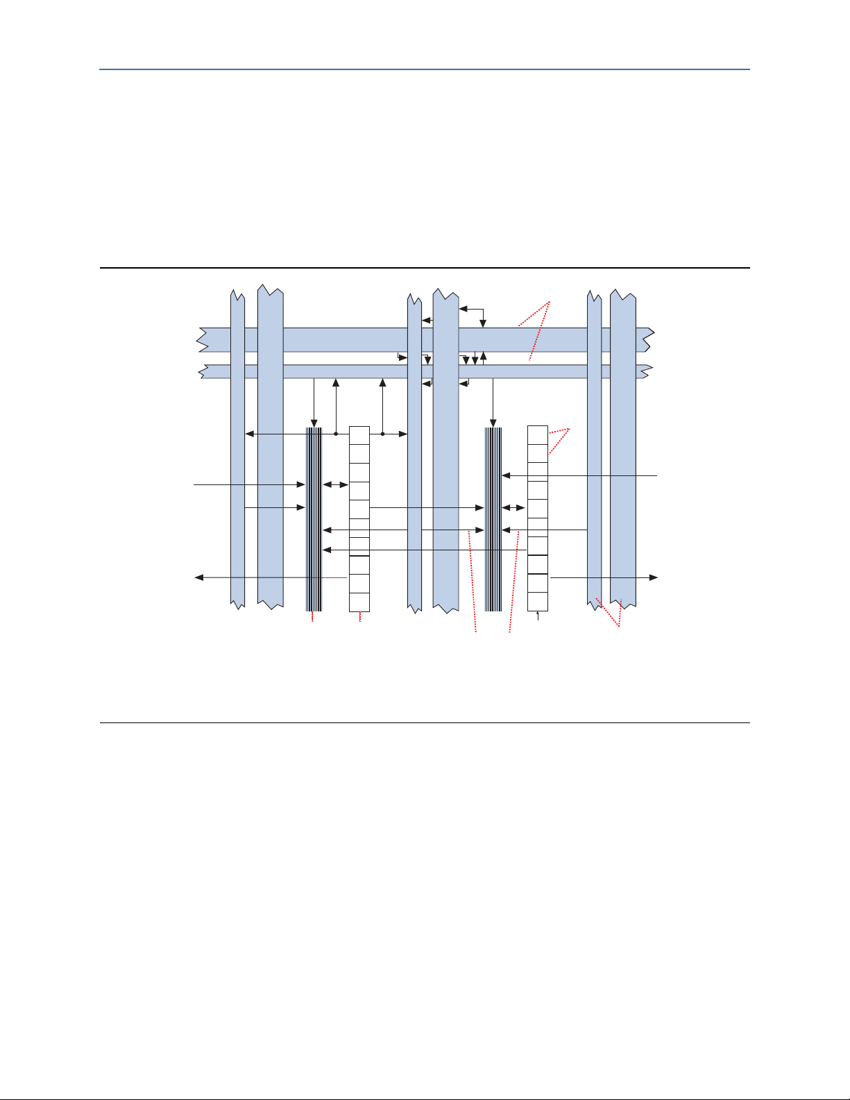
Figure 1–1 shows an overview of the Arria V LAB and MLAB structure with the LAB
interconnects.
Figure 1–1. LAB Structure and Interconnects Overview in Arria V Devices
R14
R3/R6
Direct link
interconnect from
adjacent block (1)
Direct link
interconnect to
adjacent block
C2/C4 C12
Fast local interconnect is driven
from either sides by column interconnect
and LABs, and from above by row interconnect
Row interconnects of
variable speed and length
ALMs
MLABLABLocal interconnect
Direct link
interconnect from
adjacent block
Direct link
interconnect to
adjacent block
Column interconnects of
variable speed and length
Note to Figure 1–1:
(1) Connects to adjacent LABs, memory blocks, digital signal processing (DSP) blocks, or I/O element (IOE) outputs.
Arria V Device Handbook June 2012 Altera Corporation
Volume 1: Device Interfaces and Integration
Page 17

Chapter 1: Logic Array Blocks and Adaptive Logic Modules in Arria V Devices 1–3
LAB
MLAB
Each MLAB supports a maximum of 640 bits of simple dual-port SRAM.
You can configure each ALM in an MLAB as a 32 x 2 memory block, resulting in a
configuration of 32 x 20 simple dual-port SRAM blocks.
Figure 1–2 shows the LAB and MLAB topology.
Figure 1–2. LAB and MLAB Structure for Arria V Devices
LUT-based-32 x 2
Simple dual port SRAM
LUT-based-32 x 2
Simple dual port SRAM
LUT-based-32 x 2
Simple dual port SRAM
LUT-based-32 x 2
Simple dual port SRAM
LUT-based-32 x 2
Simple dual port SRAM
(1)
(1)
(1)
(1)
(1)
ALM
ALM
ALM
ALM
ALM
LAB Control Block LAB Control Block
LUT-based-32 x 2
Simple dual port SRAM
LUT-based-32 x 2
Simple dual port SRAM
LUT-based-32 x 2
Simple dual port SRAM
LUT-based-32 x 2
Simple dual port SRAM
(1)
(1)
(1)
(1)
ALM
ALM
ALM
ALM
LUT-based-32 x 2
Simple dual port SRAM
MLAB
(1)
ALM
LAB
Note to Figure 1–2:
(1) You can use an MLAB ALM as a regular LAB ALM or configure it as a dual-port SRAM.
June 2012 Altera Corporation Arria V Device Handbook
Volume 1: Device Interfaces and Integration
Page 18
1–4 Chapter 1: Logic Array Blocks and Adaptive Logic Modules in Arria V Devices
LAB
Interconnects
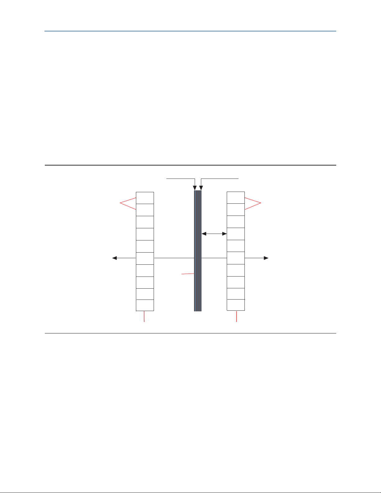
Each LAB can drive 30 ALMs through fast-local and direct-link interconnects. Ten
ALMs are in any given LAB and ten ALMs are in each of the adjacent LABs.
The local interconnect can drive ALMs in the same LAB using column and row
interconnects and ALM outputs in the same LAB.
Neighboring LABs, MLABs, M10K blocks, or digital signal processing (DSP) blocks
from the left or right can also drive the LAB’s local interconnect using the direct link
connection.
The direct link connection feature minimizes the use of row and column
interconnects, providing higher performance and flexibility.
Figure 1–3 shows the LAB fast-local and direct-link interconnects.
Figure 1–3. Direct Link and Fast Local Interconnects for Arria V Devices
Direct link interconnect from
left LAB, memory block,
DSP block, or IOE output
ALMs ALMs
Direct link
interconnect
to left
Fast local
interconnect
MLAB
LAB
Direct link interconnect from
right LAB, memory block,
DSP block, or IOE output
Direct link
interconnect
to right
Arria V Device Handbook June 2012 Altera Corporation
Volume 1: Device Interfaces and Integration
Page 19

Chapter 1: Logic Array Blocks and Adaptive Logic Modules in Arria V Devices 1–5
LAB
LAB Control Signals
Each LAB contains dedicated logic for driving the control signals to its ALMs, and has
two unique clock sources and three clock enable signals.
The LAB control block generates up to three clocks using the two clock sources and
three clock enable signals. Each clock and the clock enable signals are linked.
De-asserting the clock enable signal turns off the corresponding LAB-wide clock.
Figure 1–4 shows the clock sources and clock enable signals in an LAB.
Figure 1–4. LAB-Wide Control Signals for Arria V Devices
There are two unique
clock signals per LAB.
Dedicated Row LAB Clocks
Local Interconnect
Local Interconnect
Local Interconnect
Local Interconnect
6
6
6
(1)
labclk0
labclkena0
or asyncload
or labpreset
labclk1
labclkena1 labclkena2 labclr0 synclr
labclk2
syncload
labclr1
Note to Figure 1–4:
(1) For more information, refer to Figure 1–6 on page 1–8.
June 2012 Altera Corporation Arria V Device Handbook
Volume 1: Device Interfaces and Integration
Page 20
1–6 Chapter 1: Logic Array Blocks and Adaptive Logic Modules in Arria V Devices
LAB
ALM Registers
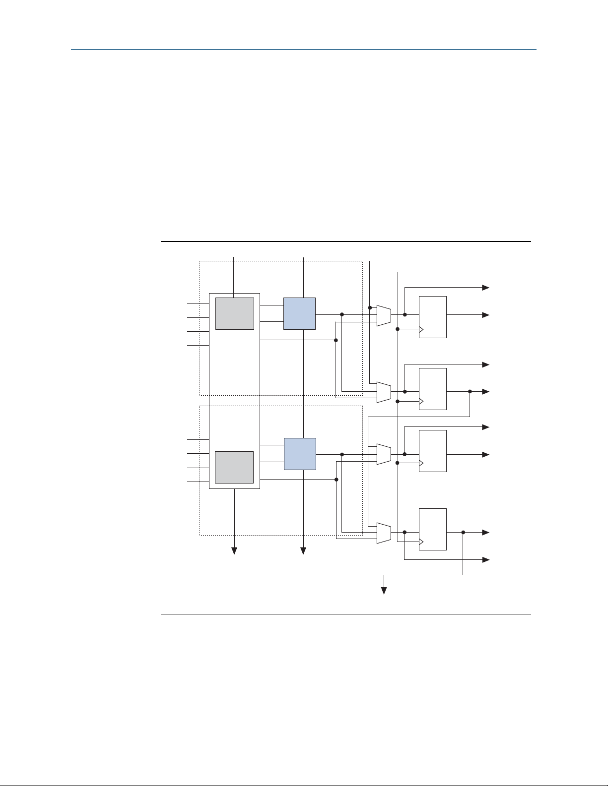
One ALM contains four programmable registers. Each register has data, clock,
synchronous and asynchronous clear, and synchronous load functions.
Global signals, general-purpose I/O (GPIO) pins, or any internal logic can drive the
clock and clear control signals of an ALM register.
GPIO pins or internal logic drives the clock enable signal.
For combinational functions, the registers are bypassed and the output of the look-up
table (LUT) drives directly to the outputs of an ALM.
Figure 1–5 shows a high-level block diagram of the Arria V ALM.
Figure 1–5. High-Level Block Diagram of the Arria V ALM
dataf0
datae0
dataa
datab
datac
datad
datae1
dataf1
shared_arith_in
6-Input LUT
6-Input LUT
carry_in
adder0
adder1
Combinational/
Memory ALUT0
Combinational/
Memory ALUT1
reg_chain_in
labclk
DQ
reg0
DQ
reg1
DQ
reg2
DQ
reg3
To general or
local routing
To general or
local routing
To general or
local routing
To general or
local routing
To general or
local routing
To general or
local routing
To general or
local routing
shared_arith_out
carry_out
reg_chain_out
To general or
local routing
1 The Quartus II software automatically configures the ALMs for optimized
performance.
Arria V Device Handbook June 2012 Altera Corporation
Volume 1: Device Interfaces and Integration
Page 21

Chapter 1: Logic Array Blocks and Adaptive Logic Modules in Arria V Devices 1–7
LAB
ALM Outputs
The LUT, adder, or register output can drive the ALM outputs. There are two sets of
outputs—general routing outputs and register chain outputs.
For each set of output drivers, two ALM outputs can drive column, row, or direct link
routing connections, and one of these ALM outputs can also drive local interconnect
resources. The LUT or adder can drive one output while the register drives another
output.
Register packing improves device utilization by allowing unrelated register and
combinational logic to be packed into a single ALM. Another mechanism to improve
fitting is to allow the register output to feed back into the look-up table (LUT) of the
same ALM so that the register is packed with its own fan-out LUT. The ALM can also
drive out registered and unregistered versions of the LUT or adder output.
June 2012 Altera Corporation Arria V Device Handbook
Volume 1: Device Interfaces and Integration
Page 22
1–8 Chapter 1: Logic Array Blocks and Adaptive Logic Modules in Arria V Devices
LAB
Figure 1–6 shows a detailed view of all the connections in an ALM.
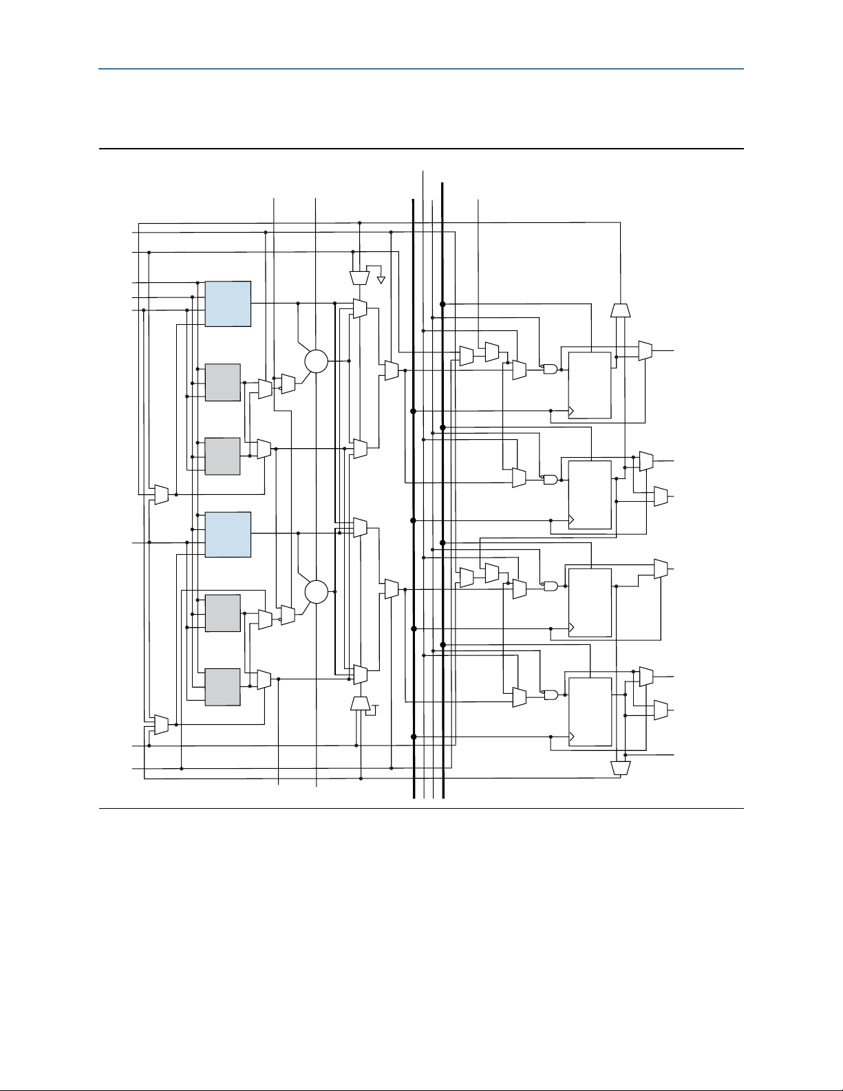
Figure 1–6. ALM Connection Details for Arria V Devices
syncload
aclr[1:0]
dataf0
datae0
shared_arith_in
carry_in
clk[2:0]
sclr
reg_chain_in
dataa
datab
datac0
datac1
4-Input
LUT
3-Input
LUT
3-Input
LUT
4-Input
LUT
3-Input
LUT
3-Input
LUT
+
+
GND
VCC
CLR
Q
D
CLR
Q
D
direct link routing
row, column
direct link routing
local
interconnect
row, column
CLR
Q
D
row, column
direct link routing
row, column
CLR
Q
D
direct link routing
local
interconnect
datae1
reg_chain_out
dataf1
shared_arith_out
Arria V Device Handbook June 2012 Altera Corporation
Volume 1: Device Interfaces and Integration
carry_out
Page 23
Chapter 1: Logic Array Blocks and Adaptive Logic Modules in Arria V Devices 1–9
ALM Operating Modes
ALM Operating Modes
The Arria V ALM operates in any of the following modes:
■ Normal Mode
■ Extended LUT Mode
■ Arithmetic Mode
■ Shared Arithmetic Mode
Normal Mode
Up to eight data inputs from the LAB local interconnect are inputs to the
combinational logic. Normal mode allows two functions to be implemented in one
Arria V ALM, or a single function of up to six inputs.
The ALM can support certain combinations of completely independent functions and
various combinations of functions that have common inputs.
Extended LUT Mode
In this mode, if the 7-input function is unregistered, the unused eighth input is
available for register packing.
1 Functions that fit into the template, as shown in Figure 1–7, often appear in designs as
“if-else” statements in Verilog HDL or VHDL code.
Figure 1–7 shows the template of supported 7-input functions using extended LUT
mode.
Figure 1–7. Template for Supported 7-Input Functions in Extended LUT Mode in Arria V Devices
datae0
datac
dataa
datab
datad
dataf0
datae1
dataf1
5-Input
LUT
5-Input
LUT
This input is available
for register packing.
combout0
DQ
reg0
To gener al or
local routing
To gener al or
local routing
June 2012 Altera Corporation Arria V Device Handbook
Volume 1: Device Interfaces and Integration
Page 24
1–10 Chapter 1: Logic Array Blocks and Adaptive Logic Modules in Arria V Devices
ALM Operating Modes
Arithmetic Mode
The ALM in arithmetic mode uses two sets of two 4-input LUTs along with two
dedicated full adders.
The dedicated adders allow the LUTs to perform pre-adder logic; therefore, each
adder can add the output of two 4-input functions.
The ALM supports simultaneous use of the adder’s carry output along with
combinational logic outputs. The adder output is ignored in this operation.
Using the adder with the combinational logic output provides resource savings of up
to 50% for functions that can use this mode.
Figure 1–8 shows an ALM in arithmetic mode.
Figure 1–8. ALM in Arithmetic Mode for Arria V Devices
carry_in
datae0
dataf0
datac
datab
dataa
4-Input
LUT
4-Input
LUT
adder0
DQ
reg0
DQ
reg1
To general or
local routing
To general or
local routing
To general or
local routing
To general or
local routing
datad
datae1
dataf1
4-Input
LUT
4-Input
LUT
carry_out
adder1
DQ
reg2
DQ
reg3
To general or
local routing
To general or
local routing
To general or
local routing
To general or
local routing
Arria V Device Handbook June 2012 Altera Corporation
Volume 1: Device Interfaces and Integration
Page 25

Chapter 1: Logic Array Blocks and Adaptive Logic Modules in Arria V Devices 1–11
ALM Operating Modes
Carry Chain
The carry chain provides a fast carry function between the dedicated adders in
arithmetic or shared arithmetic mode.
The two-bit carry select feature in Arria V devices halves the propagation delay of
carry chains within the ALM. Carry chains can begin in either the first ALM or the
fifth ALM in a LAB. The final carry-out signal is routed to an ALM, where it is fed to
local, row, or column interconnects.
To avoid routing congestion in one small area of the device when a high fan-in
arithmetic function is implemented, the LAB can support carry chains that only use
either the top half or bottom half of the LAB before connecting to the next LAB. This
leaves the other half of the ALMs in the LAB available for implementing narrower
fan-in functions in normal mode. Carry chains that use the top five ALMs in the first
LAB carry into the top half of the ALMs in the next LAB in the column. Carry chains
that use the bottom five ALMs in the first LAB carry into the bottom half of the ALMs
in the next LAB within the column. You can bypass the top-half of the LAB columns
and bottom-half of the MLAB columns.
The Quartus II Compiler creates carry chains longer than 20 ALMs (10 ALMs in
arithmetic or shared arithmetic mode) by linking LABs together automatically. For
enhanced fitting, a long carry chain runs vertically, allowing fast horizontal
connections to the TriMatrix memory and DSP blocks. A carry chain can continue as
far as a full column.
June 2012 Altera Corporation Arria V Device Handbook
Volume 1: Device Interfaces and Integration
Page 26
1–12 Chapter 1: Logic Array Blocks and Adaptive Logic Modules in Arria V Devices
ALM Operating Modes
Shared Arithmetic Mode
The ALM in shared arithmetic mode can implement a 3-input add in the ALM.
This mode configures the ALM with four 4-input LUTs. Each LUT either computes
the sum of three inputs or the carry of three inputs. The output of the carry
computation is fed to the next adder using a dedicated connection called the shared
arithmetic chain.
Figure 1–9 shows the ALM using this feature.
Figure 1–9. ALM in Shared Arithmetic Mode for Arria V Devices
shared_arith_in
carry_in
labclk
datae0
datac
datab
dataa
datad
datae1
4-Input
LUT
4-Input
LUT
4-Input
LUT
4-Input
LUT
shared_arith_out
DQ
reg0
DQ
reg1
DQ
reg2
DQ
reg3
carry_out
To general or
local routing
To general or
local routing
To general or
local routing
To general or
local routing
To general or
local routing
To general or
local routing
To general or
local routing
To general or
local routing
Shared Arithmetic Chain
The shared arithmetic chain available in enhanced arithmetic mode allows the ALM
to implement a 3-input adder. This significantly reduces the resources necessary to
implement large adder trees or correlator functions.
Similar to carry chains, the top and bottom half of the shared arithmetic chains in
alternate LAB columns can be bypassed. This capability allows the shared arithmetic
chain to cascade through half of the ALMs in an LAB while leaving the other half
available for narrower fan-in functionality. In every LAB column is top-half
bypassable; while in MLAB columns are bottom-half bypassable.
The shared arithmetic chain can begin in either the first or sixth ALM in an LAB. The
Quartus II Compiler creates shared arithmetic chains longer than 20 ALMs (10 ALMs
in arithmetic or shared arithmetic mode) by linking LABs together automatically. To
enhanced fitting, a long shared arithmetic chain runs vertically, allowing fast
horizontal connections to the TriMatrix memory and DSP blocks. A shared arithmetic
chain can continue as far as a full column.
Arria V Device Handbook June 2012 Altera Corporation
Volume 1: Device Interfaces and Integration
Page 27
Chapter 1: Logic Array Blocks and Adaptive Logic Modules in Arria V Devices 1–13
Document Revision History
Document Revision History
Table 1–1 lists the revision history for this chapter.
Table 1–1. Document Revision History
Date Version Changes
Updated for the Quartus II software v12.0 release:
June 2012 2.0
November 2011 1.1 Restructured chapter.
May 2011 1.0 Initial release.
■ Restructured chapter.
■ Updated Figure 1–6.
June 2012 Altera Corporation Arria V Device Handbook
Volume 1: Device Interfaces and Integration
Page 28

1–14 Chapter 1: Logic Array Blocks and Adaptive Logic Modules in Arria V Devices
Document Revision History
Arria V Device Handbook June 2012 Altera Corporation
Volume 1: Device Interfaces and Integration
Page 29

June 2012
AV-52002-2.0
AV-52002-2.0
2. Memory Blocks in Arria V Devices
This chapter describes the embedded memory blocks in Arria®V devices.
The memory blocks in Arria V devices provide different sizes of embedded SRAM to
fit your design requirements.
This chapter contains the following sections:
■ “Memory Types” on page 2–1
■ “Memory Features” on page 2–2
■ “Memory Modes” on page 2–3
■ “Mixed-Width Port Configurations” on page 2–4
■ “Clocking Modes” on page 2–5
■ “Parity Bit” on page 2–6
■ “Byte Enable” on page 2–6
Memory Types
f For information about the embedded memory capacity available in each Arria V
■ “Design Considerations” on page 2–8
The Arria V devices contain two types of memory blocks:
■ M10K blocks—10-kilobit (Kb) blocks of dedicated memory resources that you can
use to create designs with large memory configurations.
■ Memory logic array blocks (MLABs)—640-bit enhanced memory blocks that are
configured from dual-purpose logic array blocks (LABs). The MLABs are
optimized for implementation of shift registers for digital signal processing (DSP)
applications, wide shallow FIFO buffers, and filter delay lines. Each MLAB is
made up of ten adaptive logic modules (ALMs) that you can configure as ten
32 x 2 blocks, giving you one 32 x 20 simple dual-port SRAM block per MLAB.
device, refer to the Arria V Device Overview.
© 2012 Altera Corporation. All rights reserved. ALTERA, ARRIA, CYCLONE, HARDCOPY, MAX, MEGACORE, NIOS, QUARTUS and STRATIX words and logos
are trademarks of Altera Corporation and registered in the U.S. Patent and Trademark Office and in other countries. All other words and logos identified as
trademarks or service marks are the property of their respective holders as described at www.altera.com/common/legal.html. Altera warrants performance of its
semiconductor products to current specifications in accordance with Altera's standard warranty, but reserves the right to make changes to any products and
services at any time without notice. Altera assumes no responsibility or liability arising out of the application or use of any information, product, or service
described herein except as expressly agreed to in writing by Altera. Altera customers are advised to obtain the latest version of device specifications before relying
on any published information and before placing orders for products or services.
Arria V Device Handbook
Volume 1: Device Interfaces and Integration
June 2012
Feedback Subscribe
ISO
9001:2008
Registered
Page 30
2–2 Chapter 2: Memory Blocks in Arria V Devices
Memory Features
Memory Features
Table 2–1 summarizes the features supported by the memory blocks.
Table 2–1. Memory Features in Arria V Devices
Feature M10K MLAB
Maximum operating frequency 400 MHz 500 MHz
Total RAM bits (including parity bits) 10,240 640
256 x 32, 256 x 40,
512 x 16, 512 x 20,
Configuration (depth × width)
1K x 8, 1K x 10,
2K x 4, 2K x 5,
4K x 2, and 8K x 1
Parity bits Yes Yes
Byte enable Yes Yes
Packed mode Yes —
Address clock enable Yes Yes
■ Single-port memory
■ Simple dual-port memory
Memory modes
■ True dual-port memory
■ Embedded shift register
■ ROM
■ FIFO buffer
Simple dual-port mixed width Yes —
True dual-port mixed width Yes —
FIFO buffer mixed width Yes —
Memory Initialization File (.mif) Yes Yes
Mixed-clock mode Yes Yes
Power-up state Output ports are cleared.
Asynchronous clears Output registers
Write/Read operation triggering Rising clock edges
Output ports set to “new data” or
Same-port read-during-write
(The “don’t care” mode applies only for
“don’t care”.
the single-port RAM mode.)
Mixed-port read-during-write
Output ports set to “old data” or “don’t
care”.
ECC support Soft IP support using the Quartus
Fully synchronous memory Yes Yes
Asynchronous memory —
32 x 16, 32 x 18, and 32 x 20
■ Single-port memory
■ Simple dual-port memory
■ Embedded shift register
■ ROM
■ FIFO buffer
■ Registered output ports—Cleared.
■ Unregistered output ports—Read
memory contents.
Output ports set to “don’t care”.
Output ports set to “old data”, “new
data”, “don’t care”, or “constrained don’t
care”.
®
II software.
Only for flow-through read memory
operations.
Arria V Device Handbook June 2012 Altera Corporation
Volume 1: Device Interfaces and Integration
Page 31

Chapter 2: Memory Blocks in Arria V Devices 2–3
Memory Modes
Memory Modes
Table 2–2 lists and describes the memory modes that are supported in the Arria V
memory blocks.
c To avoid corrupting the memory contents, do not violate the setup or hold time on
any of the memory block input registers during read or write operations. This is
applicable if you use the memory blocks in single-port RAM, simple dual-port RAM,
true dual-port RAM, or ROM mode.
Table 2–2. Memory Modes Supported in the Memory Blocks
Memory Mode Description and Additional Information
You can perform only one read or one write operation at a time.
Use the read enable port to control the RAM output ports behavior during a write operation:
Single-port RAM
Simple dual-port
RAM
True dual-port RAM
Shift-register
ROM
FIFO
■ To retain the previous values that are held during the most recent active read enable—Create a
read-enable port and perform the write operation with the read enable port deasserted.
■ To show the new data being written, the old data at that address, or a “Don't Care” value when
read-during-write occurs at the same address location—Do not create a read-enable signal, or
activate the read enable during a write operation.
You can simultaneously perform one read and one write operations to different locations where the
write operation happens on port A and the read operation happens on port B.
You can perform any combination of two port operations: two reads, two writes, or one read and
one write at two different clock frequencies. This mode is available only for M10K blocks.
You can use the memory blocks as a shift-register block to save logic cells and routing resources.
This is useful in DSP applications that require local data storage such as finite impulse response
(FIR) filters, pseudo-random number generators, multi-channel filtering, and auto- and crosscorrelation functions. Traditionally, the local data storage is implemented with standard flip-flops
that exhaust many logic cells for large shift registers.
You can use the memory blocks as ROM.
■ Initialize the ROM contents of the memory blocks using a .mif or .hex.
■ The address lines of the ROM are registered on M10K blocks but can be unregistered on MLABs.
■ The outputs can be registered or unregistered.
■ The output registers can be asynchronously cleared.
■ The ROM read operation is identical to the read operation in the single-port RAM configuration.
You can use the memory blocks as FIFO buffers.
Use the SCFIFO and DCFIFO megafunctions to implement single- and dual-clock asynchronous FIFO
buffers in your design.
For designs with many small and shallow FIFO buffers, the MLABs are ideal for the FIFO mode.
However, the MLABs do not support mixed-width FIFO mode.
f For more information about each memory mode, refer to the Internal Memory (RAM
and ROM) User Guide.
f For more information about implementing the shift register mode, refer to the
RAM-Based Shift Register (ALTSHIFT_TAPS) Megafunction User Guide.
June 2012 Altera Corporation Arria V Device Handbook
Volume 1: Device Interfaces and Integration
Page 32

2–4 Chapter 2: Memory Blocks in Arria V Devices
Mixed-Width Port Configurations
f For more information about implementing FIFO buffers, refer to the SCFIFO and
DCFIFO Megafunctions User Guide.
Mixed-Width Port Configurations
The mixed-width port configuration is supported in the simple dual-port RAM and
true dual-port RAM memory modes.
f For more information about dual-port mixed width support, refer to the Internal
Memory (RAM and ROM) User Guide.
M10K Blocks Mixed-Width Configurations
Table 2–3 lists the mixed-width configurations of the M10K blocks in the simple dual-
port RAM mode.
Table 2–3. M10K Block Mixed-Width Configurations (Simple Dual-Port RAM Mode)
Write Port
Read Port
8K x 1
8K x 1 Yes Yes Yes — Yes — Yes — Yes —
4K x 2 Yes Yes Yes — Yes — Yes — Yes —
2K x 4 Yes Yes Yes — Yes — Yes — Yes —
2K x 5 — — — Yes — Yes — Yes — Yes
1K x 8 Yes Yes Yes — Yes — Yes — Yes —
1K x 10 — — — Yes — Yes — Yes — Yes
512 x 16 Yes Yes Yes — Yes — Yes — Yes —
512 x 20 — — — Yes — Yes — Yes — Yes
256 x 32 Yes Yes Yes — Yes — Yes — Yes —
256 x 40 — — — Yes — Yes — Yes — Yes
4K x 2
2K x 4
2K x 5
1K x 8
1K x 10
512 x 16
512 x 20
256 x 32
Table 2–4 lists the mixed-width configurations of the M10K blocks in true dual-port
mode.
Table 2–4. M10K Block Mixed-Width Configurations (True Dual-Port Mode) (Part 1 of 2)
Port A
Port B
8K x 1
8K x 1 Yes Yes Yes — Yes — Yes —
4K x 2 Yes Yes Yes — Yes — Yes —
2K x 4 Yes Yes Yes — Yes — Yes —
2K x 5 — — — Yes — Yes — Yes
1K x 8 Yes Yes Yes — Yes — Yes —
1K x 10 — — — Yes — Yes — Yes
4K x 2
2K x 4
2K x 5
1K x 8
1K x 10
512 x 16
256 x 40
512 x 20
Arria V Device Handbook June 2012 Altera Corporation
Volume 1: Device Interfaces and Integration
Page 33

Chapter 2: Memory Blocks in Arria V Devices 2–5
Clocking Modes
Table 2–4. M10K Block Mixed-Width Configurations (True Dual-Port Mode) (Part 2 of 2)
Port A
Port B
MLABs Mixed-Width Configurations
MLABs do not have native support for mixed-width operation. However, if you select
AUTO for your memory block type in the parameter editor, the Quartus II software
can implement mixed-width memories in MLABs by using more than one MLAB.
Clocking Modes
This section describes the clocking modes for the Arria V memory blocks.
c To avoid corrupting the memory contents, do not violate the setup or hold time on the
memory block address registers during read or write operations.
Clocking Modes for Each Memory Mode
Table 2–5 lists the memory blocks clocking modes supported in the Arria V devices
and the memory modes supported by each clocking mode.
Table 2–5. Memory Blocks Clocking Modes for Each Memory Mode
8K x 1
512 x 16 Yes Yes Yes — Yes — Yes —
512 x 20 — — — Yes — Yes — Yes
4K x 2
2K x 4
2K x 5
1K x 8
1K x 10
512 x 16
512 x 20
Memory Mode
Clocking Mode
Single-Port
Single clock mode Yes Yes Yes Yes Yes
Read/write clock mode — Yes — — Yes
Input/output clock mode Yes Yes Yes Yes —
Independent clock mode — — Yes Yes —
Simple
Dual-Port
True
Dual-Port
ROM FIFO
f For more information about each clocking mode, refer to the Internal Memory (RAM
and ROM) User Guide.
Asynchronous Clears
In all clocking modes, asynchronous clears are available only for output latches and
output registers. For the independent clock mode, this is applicable on both ports.
June 2012 Altera Corporation Arria V Device Handbook
Volume 1: Device Interfaces and Integration
Page 34

2–6 Chapter 2: Memory Blocks in Arria V Devices
Parity Bit
Output Read Data in Simultaneous Read/Write
If you perform a simultaneous read/write to the same address location using the
read/write clock mode, the output read data is unknown. If you require the output
read data to be a known value, use single-clock or input/output clock mode and
select the appropriate read-during-write behavior in the MegaWizard Plug-In
Manager.
Independent Clock Enables
Independent clock enables are supported in the following clocking modes:
■ Read/write clock mode—supported for both the read and write clocks.
■ Independent clock mode—supported for the registers of both ports.
To save power, you can control the shut down of a particular register using the clock
enables. For more information, refer to “Power Management” on page 2–13.
Parity Bit
Table 2–6 describes the parity bit support for the memory blocks.
Byte Enable
Table 2–6. Parity Bit Support for the Memory Blocks
M10K MLAB
■ The parity bit is the fifth bit associated with
each 4 data bits in data widths of 5, 10, 20,
and 40 (bits 4, 9, 14, 19, 24, 29, 34, and 39).
■ In non-parity data widths, the parity bits are
skipped during read or write operations.
■ Parity function is not performed on the parity
■ The parity bit is the ninth bit associated with
each byte.
■ The ninth bit can store a parity bit or serve as
an additional bit.
■ Parity function is not performed on the parity
bit.
bit.
The memory blocks support byte enable controls:
■ The byte enable controls mask the input data so that only specific bytes of data are
written. The unwritten bytes retain the values written previously.
■ The write enable (
control the write operations on the RAM blocks. By default, the
high (enabled) and only the
■ The byte enable registers do not have a
■ If you are using parity bits, on the M10K blocks, the byte enable function controls
wren
) signal, together with the byte enable (
wren
signal controls the writing.
clear
port.
byteena
byteena
) signal,
signal is
8 data bits and 2 parity bits; on the MLABs, the byte enable function controls all 10
bits in the widest mode.
■ The MSB and LSB of the
byteena
signal correspond to the MSB and LSB of the data
bus, respectively.
■ The byte enables are active high.
Arria V Device Handbook June 2012 Altera Corporation
Volume 1: Device Interfaces and Integration
Page 35

Chapter 2: Memory Blocks in Arria V Devices 2–7
Byte Enable
byteena Controls
Table 2–7 lists the
Table 2–7. byteena Controls in x20 Data Width
Table 2–8 lists the
Table 2–8. byteena Controls in x40 Data Width
byteena[3:0] Data Bits Written
1111 (default)
1000
0100 —
0010 — —
0001 — — —
Data Byte Output
byteena
byteena[1:0] Data Bits Written
11 (default)
10
01 —
byteena
controls in the x20 data widths.
[19:10] [9:0]
[19:10]
controls in the x40 data widths.
[39:30] [29:20] [19:10] [9:0]
[39:30]
———
[29:20]
——
[19:10]
—
[9:0]
—
[9:0]
In M10K blocks, the corresponding masked data byte output appears as a “don’t care”
value.
In MLABs, when a byte-enable bit is deasserted during a write cycle, the
corresponding data byte output appears as either a “don’t care” value or the current
data at that location. You can control the output value for the masked byte in MLABs
using the Quartus II software.
June 2012 Altera Corporation Arria V Device Handbook
Volume 1: Device Interfaces and Integration
Page 36

2–8 Chapter 2: Memory Blocks in Arria V Devices
Design Considerations
RAM Blocks Operations
Figure 2–1 shows how the
RAM blocks.
Figure 2–1. Byte Enable Functional Waveform
inclock
wren
address
data
byteena
contents at a0
contents at a1
contents at a2
contents at a3
contents at a4
don’t care: q (asynch)
an a0 a1 a2 a3 a4 a0
XXXXXXXX XXXXXXXXABCDEF12
XXXX XXXX1000 0100 0010 0001 1111
FFFFFFFF
FFFFFFFF
FFFFFFFF
ABXXXXXX XXCDXXXX XXXXEFXX XXXXXX12 ABCDEF12
(1)
FFFFFFFF
wren
FFFFFFFF
and
byteena
signals control the operations of the
ABFFFFFF
FFCDFFFF
FFFFEFFF
FFFFFF12
ABCDEF12
ABFFFFFFdoutn
current data: q (asynch)
Note to Figure 2–1:
(1) For the M10K blocks, the write-masked data byte output appears as a “don’t care” value because the “current data” value is not supported.
doutn
ABFFFFFF
FFCDFFFF
FFFFEFFF
FFFFFF12
ABFFFFFFABCDEF12
Design Considerations
To ensure the success of your designs using the memory blocks in Arria V devices,
take into consideration the following guidelines when you are designing with the
memory blocks.
Memory Block Selection
The Quartus II software automatically partitions the user-defined memory into the
memory blocks based on the speed and size constraints placed on your design. For
example, the Quartus II software may spread out the memory across multiple
available memory blocks to increase the performance of the design.
To assign the memory to a specific block size manually, use the RAM megafunction in
the MegaWizard™Plug-In Manager.
For the MLABs, you can implement single-port SRAM through emulation using the
Quartus II software. Emulation results in minimal additional use of logic resources.
Arria V Device Handbook June 2012 Altera Corporation
Volume 1: Device Interfaces and Integration
Page 37

Chapter 2: Memory Blocks in Arria V Devices 2–9
Design Considerations
Because of the dual-purpose architecture of the MLAB, only data input registers and
output registers are available in the block. The MLABs gain read address registers
from the ALMs. However, the write address and read data registers are internal to the
MLABs.
Conflict Resolution
In the true dual-port RAM mode, you can perform two write operations to the same
memory location. However, the memory blocks do not have internal conflict
resolution circuitry. To avoid unknown data being written to the address, implement
external conflict resolution logic to the memory block.
Read-During-Write Behavior
Customize the read-during-write behavior of the memory blocks to suit your design
requirements.
Figure 2–2 shows the difference between the two types of read-during-write
operations available—same port and mixed port.
Figure 2–2. Read-During-Write Data Flow for Arria V Devices
FPGA Device
Por t A
data in
Por t A
data out
Por t B
data in
Mixed-port
data flow
Same-port
data flow
Por t B
data out
Same-Port Read-During-Write Mode
The same-port read-during-write mode applies to a single-port RAM or the same port
of a true dual-port RAM.
Table 2–9 lists the available output modes if you select the M10K or MLAB in the
same-port read-during-write mode.
Table 2–9. Output Modes for M10K or MLAB in Same-Port Read-During-Write Mode
Output Mode Memory Type Description
“new data”
(flow-through)
M10K
“don’t care” M10K, MLAB
The new data is available on the rising edge of the same clock
cycle on which the new data is written.
The RAM outputs “don’t care” values for a read-during-write
operation.
June 2012 Altera Corporation Arria V Device Handbook
Volume 1: Device Interfaces and Integration
Page 38

2–10 Chapter 2: Memory Blocks in Arria V Devices
Design Considerations
Figure 2–3 shows sample functional waveforms of same-port read-during-write
behavior in the “new data” mode.
Figure 2–3. Same-Port Read-During-Write: New Data Mode
clk_a
address
rden
wren
byteena
data_a
q_a (asynch)
A123 B456 C789 DDDD EEEE FFFF
A123 B456 C789 DDDD EEEE FFFF
0A 0B
11
Mixed-Port Read-During-Write Mode
The mixed-port read-during-write mode applies to simple and true dual-port RAM
modes where two ports perform read and write operations on the same memory
address using the same clock—one port reading from the address, and the other port
writing to it.
Table 2–10 lists the available output modes in the mixed-port read-during-write
mode.
Table 2–10. Output Modes for RAM in Mixed-Port Read-During-Write Mode
Output Mode Memory Type Description
A read-during-write operation to different ports causes the
“new data” MLAB
“old data” M10K, MLAB
“don’t care” M10K, MLAB
“constrained
don’t care”
MLAB
MLAB registered output to reflect the “new data” on the next
rising edge after the data is written to the MLAB memory.
This mode is available only if the output is registered.
A read-during-write operation to different ports causes the RAM
output to reflect the “old data” value at the particular address.
For MLAB, this mode is available only if the output is registered.
The RAM outputs “don’t care” or “unknown” value.
For MLAB, the Quartus II software does not analyze the timing
between write and read operations. To prevent metastability
issue at the MLAB output, never write and read the same
address at the same time.
For M10K memory, the Quartus II software analyzes the timing
between write and read operations.
The RAM outputs “don’t care” or “unknown” value. The
Quartus II software analyzes the timing between write and read
operations in the MLAB.
Arria V Device Handbook June 2012 Altera Corporation
Volume 1: Device Interfaces and Integration
Page 39

Chapter 2: Memory Blocks in Arria V Devices 2–11
Design Considerations
Figure 2–4 shows a sample functional waveform of mixed-port read-during-write
behavior for the “new data” mode.
Figure 2–4. Mixed-Port Read-During-Write: New Data Mode
clk_a&b
wren_a
address_a
data_a
byteena_a
rden_b
address_b
q_b (registered)
AAAA BBBB CCCC DDDD EEEE FFFF
XXXX
A0 A1
11
A0 A1
AAAA BBBB CCCC DDDD EEEE FFFF
Figure 2–5 shows a sample functional waveform of mixed-port read-during-write
behavior for the “old data” mode.
Figure 2–5. Mixed-Port Read-During-Write: Old Data Mode
clk_a&b
wren_a
address_a
data_a
byteena_a
AAAA BBBB CCCC DDDD EEEE FFFF
A0 A1
11
rden_b
address_b
q_b (asynch)
June 2012 Altera Corporation Arria V Device Handbook
A0 (old data) AAAA BBBB DDDD EEEEA1 (old data)
A0 A1
Volume 1: Device Interfaces and Integration
Page 40

2–12 Chapter 2: Memory Blocks in Arria V Devices
Design Considerations
Figure 2–6 shows a sample functional waveform of mixed-port read-during-write
behavior for the “don’t care” or “constrained don’t care” mode.
Figure 2–6. Mixed-Port Read-During-Write: Don’t Care or Constrained Don’t Care Mode
clk_a&b
wren_a
address_a
data_a
byteena_a
rden_b
address_b
q_b (asynch) XXXX (unknown data)
AAAA BBBB CCCC DDDD EEEE FFFF
11
A0
01 10
A0
In the dual-port RAM mode, the mixed-port read-during-write operation is
supported if the input registers have the same clock. The output value during the
operation is “unknown.”
f For more information about the RAM megafunction that controls the
read-during-write behavior, refer to the Internal Memory (RAM and ROM) User Guide.
Power-Up State and Memory Initialization
Consider the power up state of the different types of memory blocks if you are
designing logic that evaluates the initial power-up values, as listed in Table 2–11.
A1
11
A1
Table 2–11. Initial Power-Up Values of M10K and MLAB Blocks
Memory Type Output Registers Power Up Value
M10K
MLAB
Used Zero (cleared)
Bypassed Zero (cleared)
Used Zero (cleared)
Bypassed Read memory contents
By default, the Quartus II software initializes the RAM cells in Arria V devices to zero
unless you specify a .mif.
All memory blocks support initialization with a .mif. You can create .mif files in the
Quartus II software and specify their use with the RAM megafunction when you
instantiate a memory in your design. Even if a memory is pre-initialized (for example,
using a .mif), it still powers up with its output cleared.
f For more information about .mif files, refer to the Internal Memory (RAM and ROM)
User Guide and the Quartus II Handbook.
Arria V Device Handbook June 2012 Altera Corporation
Volume 1: Device Interfaces and Integration
Page 41

Chapter 2: Memory Blocks in Arria V Devices 2–13
Document Revision History
Power Management
Reduce AC power consumption in your design by controlling the clocking of each
memory block:
■ Use the read-enable signal to ensure that read operations occur only when
required. If your design does not require read-during-write, you can reduce your
power consumption by deasserting the read-enable signal during write
operations, or during the period when no memory operations occur.
■ Use the Quartus II software to automatically place any unused memory blocks in
low-power mode to reduce static power.
Document Revision History
Table 2–12 lists the revision history for this chapter.
Table 2–12. Document Revision History
Date Version Changes
■ Restructured the chapter.
■ Updated the “Memory Modes”, “Clocking Modes”, and “Design Considerations” sections.
June 2012 2.0
November 2011 1.1
May 2011 1.0 Initial release.
■ Updated Table 2–1.
■ Added the “Parity Bit” and “Byte Enable” sections.
■ Moved the memory capacity information to the Arria V Device Overview.
■ Updated Table 2–1.
■ Restructured chapter.
June 2012 Altera Corporation Arria V Device Handbook
Volume 1: Device Interfaces and Integration
Page 42

2–14 Chapter 2: Memory Blocks in Arria V Devices
Document Revision History
Arria V Device Handbook June 2012 Altera Corporation
Volume 1: Device Interfaces and Integration
Page 43

June 2012
AV-52003-2.0
AV-52003-2.0
Features
3. Variable-Precision DSP Blocks in Arria V Devices
This chapter describes how the variable-precision digital signal processing (DSP)
blocks in Arria®V devices are optimized to support higher bit precision in
high-performance DSP applications.
This chapter contains the following sections:
■ “Features”
■ “Supported Operational Modes” on page 3–2
■ “Design Considerations” on page 3–3
■ “Block Architecture” on page 3–4
■ “Operational Mode Descriptions” on page 3–9
Arria V variable-precision DSP blocks offer the following:
■ High-performance, power-optimized, and fully registered multiplication
operations
■ 9-bit, 18-bit, and 27-bit word lengths
■ Two 18 x 19 complex multiplications
■ Built-in addition, subtraction, and dual 64-bit accumulation unit to combine
multiplication results
■ Cascading 19-bit or 27-bit to form the tap-delay line for filtering applications
■ Cascading 64-bit output bus to propagate output results from one block to the next
block without external logic support
■ Hard pre-adder supported in 19-bit and 27-bit mode for symmetric filters
■ Internal coefficient register bank for filter implementation
■ 18-bit and 27-bit systolic finite impulse response (FIR) filters with distributed
output adder
f For more information about the number of multipliers in each Arria V device, refer to
the Arria V Device Overview.
© 2012 Altera Corporation. All rights reserved. ALTERA, ARRIA, CYCLONE, HARDCOPY, MAX, MEGACORE, NIOS, QUARTUS and STRATIX words and logos
are trademarks of Altera Corporation and registered in the U.S. Patent and Trademark Office and in other countries. All other words and logos identified as
trademarks or service marks are the property of their respective holders as described at www.altera.com/common/legal.html. Altera warrants performance of its
semiconductor products to current specifications in accordance with Altera's standard warranty, but reserves the right to make changes to any products and
services at any time without notice. Altera assumes no responsibility or liability arising out of the application or use of any information, product, or service
described herein except as expressly agreed to in writing by Altera. Altera customers are advised to obtain the latest version of device specifications before relying
on any published information and before placing orders for products or services.
Arria V Device Handbook
Volume 1: Device Interfaces and Integration
June 2012
Feedback Subscribe
ISO
9001:2008
Registered
Page 44

3–2 Chapter 3: Variable-Precision DSP Blocks in Arria V Devices
Supported Operational Modes
Supported Operational Modes
Table 3–1 summarizes the operational modes that are supported by Arria V
variable-precision DSP blocks.
Table 3–1. Variable-Precision DSP Blocks Operational Modes for Arria V Devices
Variable-Precision
DSP Block Resource
Operation Mode
Supported
Instance
Independent 9 x 9 multiplication 3 No No No No
Independent 18 x 18 multiplication 2 Yes Yes Yes No
Independent 18 x 19 multiplication 2 Yes Yes Yes No
1 variable-precision
DSP block
Independent 18 x 25 multiplication 1 Yes Yes Yes Yes
Independent 20 x 24 multiplication 1 Yes Yes Yes Yes
Independent 27 x 27 multiplication 1 Yes Yes Yes Yes
Two 18 x 19 multiplier adder mode 1 Yes Yes Yes Yes
18 x 18 multiplier adder summed
with 36-bit input
2 variable-precision
DSP blocks
Note to Table 3–1:
(1) When you enable the pre-adder feature, the input cascade support is not available.
Complex 18 x 19 multiplication 1 No No Yes No
1 Yes No No Yes
Pre-Adder
Support
Coefficient
Support
Input
Cascade
Support
(1)
Chainout
Support
Arria V Device Handbook June 2012 Altera Corporation
Volume 1: Device Interfaces and Integration
Page 45

Chapter 3: Variable-Precision DSP Blocks in Arria V Devices 3–3
Design Considerations
Design Considerations
Operational Modes
The Quartus®II software includes megafunctions that you can use to control the
operation mode of the multipliers. After entering the parameter settings with the
MegaWizard
variable-precision DSP block.
f For more information, refer to the following user guides:
■ Introduction to Megafunction User Guide
■ Integer Arithmetic Megafunctions User Guide
■ Floating-Point Megafunctions User Guide
Pre-Adder
To use the pre-adder feature, all input data and multipliers must have the same clock
setting.
™
Plug-In Manager, the Quartus II software automatically configures the
The input cascade support is not available when you enable the pre-adder feature.
Internal Coefficient
In both 18-bit and 27-bit modes, you can use the coefficient feature and pre-adder
feature independently.
Accumulator
The accumulator supports double accumulation by enabling the 64-bit double
accumulation registers located between the output register bank and the accumulator.
The double accumulation registers are set statically in the programming file.
Chainout Adder
You can use the output chaining path to add results from other DSP blocks.
June 2012 Altera Corporation Arria V Device Handbook
Volume 1: Device Interfaces and Integration
Page 46

3–4 Chapter 3: Variable-Precision DSP Blocks in Arria V Devices
Block Architecture
Block Architecture
The Arria V variable-precision DSP block consists of the following elements:
■ Input Register Bank
■ Pre-Adder
■ Internal Coefficient
■ Multipliers
■ Adder
■ Accumulator and Chainout Adder
■ Systolic Registers
■ Double Accumulation Register
■ Output Register Bank
Figure 3–1 shows an overall architecture of the Arria V variable-precision DSP block.
Figure 3–1. Variable-Precision DSP Block Architecture for Arria V Devices
Multiplier
x
Multiplier
x
CLK[2..0]
ENA[2..0]
ACLR[1..0]
+/-
+/-
Adder
LOADCONST
ACCUMULATE
NEGATE
SUB_COMPLEX
dataa_y0[18..0]
dataa_z0[17..0]
dataa_x0[17..0]
COEFSELA[2..0]
datab_y1[18..0]
datab_z1[17..0]
datab_x1[17..0]
COEFSELB[2..0]
scanin
Input Register Bank
scanout
Pre-Adder
+/-
Pre-Adder
+/-
Internal
Coefficient
Internal
Coefficient
Systolic
Registers
(2)
(1)
chainin[63..0]
+/-
Systolic
Register (2)
+
Chainout adder/
accumulator
Notes to Figure 3–1:
(1) If the variable-precision DSP block is not configured in systolic FIR mode, both systolic registers are bypassed.
(2) When enabled, systolic registers are clocked with the same clock source as the output register bank.
Constant
Output Register Bank
chainout[63..0]
Double
Accumulation
Register
Result[73..0]
Arria V Device Handbook June 2012 Altera Corporation
Volume 1: Device Interfaces and Integration
Page 47

Chapter 3: Variable-Precision DSP Blocks in Arria V Devices 3–5
Block Architecture
Input Register Bank
The input register bank consists of data, dynamic control signals, and two sets of
delay registers.
All the registers in the DSP blocks are positive-edge triggered and cleared on power
up. Each multiplier operand can feed an input register or a multiplier directly,
bypassing the input registers.
The following variable-precision DSP block signals control the input registers within
the variable-precision DSP block:
■
CLK[2..0]
■
ENA[2..0]
■
ACLR[0]
In 18 x 19 mode, you can use the delay registers to balance the latency requirements
when you use both the input cascade and chainout features.
The tap-delay line feature allows you to drive the top leg of the multiplier input,
dataa_y0
general routing or cascade chain.
and
datab_y1
in 18 x 19 mode and
dataa_y0
only in 27 x 27 mode, from the
Figure 3–2 shows the input register for 18 x19 mode.
Figure 3–2. Input Register of a Variable-Precision DSP Block in 18 x 19 Mode
CLK[2..0]
scanin[18..0]
dataa_y0[18..0]
dataa_z0[17..0]
dataa_x0[17..0]
Delay registers
datab_y1[18..0]
datab_z1[17..0]
datab_x1[17..0]
ENA[2..0]
ACLR[0]
(1)
Delay registers
scanout[18..0]
Note to Figure 3–2:
(1) This figure shows the data registers only. Registers for the control signals are not shown.
June 2012 Altera Corporation Arria V Device Handbook
Volume 1: Device Interfaces and Integration
Page 48

3–6 Chapter 3: Variable-Precision DSP Blocks in Arria V Devices
Block Architecture
Figure 3–3 shows the input register for 27 x 27 mode.
Figure 3–3. Input Register of a Variable-Precision DSP Block in 27 x 27 Mode
CLK[2..0]
ENA[2..0]
scanin[26..0]
dataa_y0[26..0]
dataa_z0[25..0]
dataa_x0[26..0]
Note to Figure 3–3:
(1) This figure shows the data registers only. Registers for the control signals are not shown.
ACLR[0]
scanout[26..0]
(1)
Pre-Adder
Each variable-precision DSP block has two 19-bit pre-adders. You can configure these
pre-adders as two 19-bit pre-adders or one 27-bit pre-adder.
The pre-adder supports both addition and substraction in the following input
configurations:
■ 18-bit (signed) addition or subtraction for 18 x 19 mode
■ 17-bit (unsigned) addition or subtraction for 18 x 19 mode
■ 26-bit addition or subtraction for 27 x 27 mode
Internal Coefficient
The Arria V variable-precision DSP block has the flexibility of selecting the
multiplicand from either the dynamic input or the internal coefficient.
The internal coefficient can support up to eight constant coefficients for the
multiplicands in 18-bit and 27-bit modes. When you enable the internal coefficient
feature,
multiplexer.
COEFSELA/COEFSELB
are used to control the selection of the coefficient
Arria V Device Handbook June 2012 Altera Corporation
Volume 1: Device Interfaces and Integration
Page 49

Chapter 3: Variable-Precision DSP Blocks in Arria V Devices 3–7
Block Architecture
Multipliers
A single variable-precision DSP block can perform many multiplications in parallel,
depending on the data width of the multiplier.
There are two multipliers per variable-precision DSP block.
You can configure these two multipliers to the following operational modes:
■ One 27 x 27 multiplier
■ Two 18 (signed)/(unsigned) x 19 (signed) multipliers
■ Three 9 x 9 multipliers
For more information about the operational modes of the multipliers, refer to
“Operational Mode Descriptions” on page 3–9.
Adder
You can use the adder in various sizes, depending on the operational mode:
■ one 64-bit adder with the 64-bit accumulator
■ two 18 x 19 modes—the adder is divided into two 37-bit adders to produce the full
37-bit result of each independent 18 x 19 multiplication
■ three 9 x 9 modes—you can use the adder as three 18-bit adders to produce three
9x9multiplication results independently
Accumulator and Chainout Adder
The Arria V variable-precision DSP block supports a 64-bit accumulator and a 64-bit
adder.
The following signals can dynamically control the function of the accumulator:
■
NEGATE
■
LOADCONST
■
ACCUMULATE
The accumulator supports double accumulation by enabling the 64-bit double
accumulation registers located between the output register bank and the accumulator.
The double accumulation registers are set statically in the programming file.
The accumulator and chainout adder features are not supported in two independent
18 x 19 modes and three independent 9 x 9 modes.
June 2012 Altera Corporation Arria V Device Handbook
Volume 1: Device Interfaces and Integration
Page 50

3–8 Chapter 3: Variable-Precision DSP Blocks in Arria V Devices
Block Architecture
Table 3–2 lists the dynamic signals settings and description for each function.
Table 3–2. Dynamic Control Signals for 64-Bit Accumulator in Arria V Devices
Function Description NEGATE LOADCONST ACCUMULATE
Zeroing Disables the accumulator. 0 0 0
Loads an initial value to the accumulator. Only one bit of the
Preload
Accumulation Adds the current result to the previous accumulate result. 0 X
Decimation
Note to Table 3–2:
(1) X denotes a “don’t care” value.
64-bit preload value can be “1”. It can be used as rounding
the DSP result to any position of the 64-bit result.
This function takes the current result, converts it into two’s
complement, and adds it to the previous result.
01 0
(1)
1X
(1)
1
1
Systolic Registers
There are two systolic registers per variable-precision DSP block. If the
variable-precision DSP block is not configured in systolic FIR mode, both systolic
registers are bypassed.
The first set of systolic registers consists of 18-bit and 19-bit registers that are used to
register the 18-bit and 19-bit inputs of the upper multiplier, respectively.
The second set of systolic registers are used to delay the chainout output to the next
variable-precision DSP block.
You must clock all the systolic registers with the same clock source as the output
register bank.
Double Accumulation Register
The double accumulation register is an extra register in the feedback path of the
accumulator. Enabling the double accumulation register will cause an extra clock
cycle delay in the feedback path of the accumulator.
This register has the same
By enabling this register, you can have two accumulator channels using the same
number of variable precision DSP block.
Output Register Bank
The positive edge of the clock signal triggers the 64-bit bypassable output register
bank and is cleared after power up.
The following variable-precision DSP block signals control the output register
per variable-precision DSP block:
CLK,ENA
, and
ACLR
settings as the output register bank.
■
CLK[2..0]
■
ENA[2..0]
■
ACLR[1]
Arria V Device Handbook June 2012 Altera Corporation
Volume 1: Device Interfaces and Integration
Page 51

Chapter 3: Variable-Precision DSP Blocks in Arria V Devices 3–9
Operational Mode Descriptions
Operational Mode Descriptions
This section describes how you can configure an Arria V variable-precision DSP block
to efficiently support the following operational modes:
■ Independent Multiplier Mode
■ Independent Complex Multiplier Mode
■ Multiplier Adder Sum Mode
■ 18 x 18 Multiplication Summed with 36-Bit Input Mode
■ Systolic FIR Mode
Independent Multiplier Mode
In independent input and output multiplier mode, the variable-precision DSP blocks
perform individual multiplication operations for general purpose multipliers.
Table 3–3 lists the Arria V variable-precision DSP block multiplier configurations for
the independent multiplier mode.
Table 3–3. Variable-Precision DSP Block Independent Multiplier Mode Configurations
Configuration Multipliers per block Description
9x9 3 Figure 3–4
18 (signed) x 18 (unsigned)
18 (unsigned) x 18 (unsigned)
18 (signed) x 19 (signed)
2 Figure 3–5
18 (unsigned) x 19 (signed)
18x25 1 Figure 3–6
20x24 1 Figure 3–7
27x27 1 Figure 3–8
Figure 3–4 shows the variable-precision DSP block in9x9independent multiplier
mode.
Figure 3–4. Three 9 x 9 Independent Multiplier Mode per Variable-Precision DSP Block
Variable-Precision DSP Block
Multiplier
ay[y2, y1, y0]
ax[x2, x1, x0]
27
27
Input Register Bank
x
54
Output Register Bank
(1)
Result[53..0]
(p2, p1, p0)
Note to Figure 3–4:
(1) Three pairs of data are packed into theaxandayports;
June 2012 Altera Corporation Arria V Device Handbook
result
contains three 18-bit products.
Volume 1: Device Interfaces and Integration
Page 52

3–10 Chapter 3: Variable-Precision DSP Blocks in Arria V Devices
Operational Mode Descriptions
Figure 3–5 shows the variable-precision DSP block in 18 x 18 or 18 x 19 independent
multiplier mode.
Figure 3–5. Two 18 x 18 or 18 x 19 Independent Multiplier Mode per Variable-Precision DSP
(1), (2)
Block
data_b1[(n-1)..0]
data_a1[17..0]
data_b0[(n-1)..0]
data_a0[17..0]
Variable-Precision DSP Block
n
18
n
Input Register Bank
18
Multiplier
x
Multiplier
x
m
[(m-1)..0]
Output Register Bank
m
[(m-1)..0]
Notes to Figure 3–5:
(1) n = 19 and m = 37 for 18 x 19 mode.
(2) n = 18 and m = 36 for 18 x 18 mode.
Figure 3–6 shows the variable-precision DSP block in 18 x 25 independent multiplier
mode.
Figure 3–6. One 18 x 25 Independent Multiplier Mode per Variable-Precision DSP Block
(1)
Variable-Precision DSP Block
Multiplier
dataa_b0[17..0]
dataa_a0[24..0]
18
25
Input Register Bank
x
43
Output Register Bank
Note to Figure 3–6:
(1) The result can be up to 52 bits when combined with a chainout adder or accumulator.
Result[42..0]
Arria V Device Handbook June 2012 Altera Corporation
Volume 1: Device Interfaces and Integration
Page 53

Chapter 3: Variable-Precision DSP Blocks in Arria V Devices 3–11
Operational Mode Descriptions
Figure 3–7 shows the variable-precision DSP block in 20 x 24 independent multiplier
mode.
Figure 3–7. One 20 x 24 Independent Multiplier Mode per Variable-Precision DSP Block
dataa_b0[19..0]
dataa_a0[23..0]
Variable-Precision DSP Block
20
24
Input Register Bank
Multiplier
x
44
Output Register Bank
(1)
Result[43..0]
Note to Figure 3–7:
(1) The result can be up to 52 bits when combined with a chainout adder or accumulator.
Figure 3–8 shows the variable-precision DSP block in 27 x 27 independent multiplier
mode.
Figure 3–8. One 27 x 27 Independent Multiplier Mode per Variable-Precision DSP Block
Variable-Precision DSP Block
Multiplier
27
dataa_b0[26..0]
dataa_a0[26..0]
x
27
Input Register Bank
54
Output Register Bank
(1)
Result[53..0]
Note to Figure 3–8:
(1) The result can be up to 64 bits when combined with a chainout adder or accumulator.
June 2012 Altera Corporation Arria V Device Handbook
Volume 1: Device Interfaces and Integration
Page 54

3–12 Chapter 3: Variable-Precision DSP Blocks in Arria V Devices
Operational Mode Descriptions
Independent Complex Multiplier Mode
The Arria V devices support the 18 x 19 complex multiplier mode using two Arria V
variable-precision DSP blocks.
Equation 3–1 shows a sample complex multiplication equation.
Equation 3–1. Complex Multiplication Equation
ajb+()cjd+()× ac×()bd×()–[]ja d×()bc×()+[]+=
The imaginary part [(a × d)+(b× c)] is implemented in the first variable-precision
DSP block, while the real part [(a × c)-(b× d)] is implemented in the second
variable-precision DSP block.
Figure 3–9 shows an 18 x 19 complex multiplication.
Figure 3–9. One 18 x 19 Complex Multiplier with Two Variable-Precision DSP Blocks
Variable-Precision DSP Block 1
Multiplier
c[18..0]
b[17..0]
d[18..0]
a[17..0]
d[18..0]
b[17..0]
c[18..0]
a[17..0]
19
18
19
Input Register Bank
18
Variable-Precision DSP Block 2
19
18
19
Input Register Bank
18
x
Multiplier
x
Multiplier
x
Multiplier
x
Adder
+
Adder
-
37
Imaginary Part
(ad+bc)
Output Register Bank
37
Real Part
(ac-bd)
Output Register Bank
Arria V Device Handbook June 2012 Altera Corporation
Volume 1: Device Interfaces and Integration
Page 55

Chapter 3: Variable-Precision DSP Blocks in Arria V Devices 3–13
Operational Mode Descriptions
Multiplier Adder Sum Mode
Figure 3–10 shows the variable-precision DSP blocks in one sum of two 18 x 19
multipliers adder sum mode.
Figure 3–10. One Sum of Two 18 x 19 Multipliers with One Variable-Precision DSP Block
Variable-Precision DSP Block
SUB_COMPLEX
dataa_y0[18..0]
dataa_x0[17..0]
datab_y1[18..0]
datab_x1[17..0]
19
18
19
Input Register Bank
18
Multiplier
x
Multiplier
x
+/-
Adder
Chainout adder or
accumulator
+
37
Result[36..0]
Output Register Bank
June 2012 Altera Corporation Arria V Device Handbook
Volume 1: Device Interfaces and Integration
Page 56

3–14 Chapter 3: Variable-Precision DSP Blocks in Arria V Devices
Operational Mode Descriptions
18 x 18 Multiplication Summed with 36-Bit Input Mode
Arria V variable-precision DSP blocks support one 18 x 18 multiplication summed to
a 36-bit input.
Use the upper multiplier to provide the input for an 18 x 18 multiplication, while the
bottom multiplier is bypassed. The
are concatenated to produce a 36-bit input.
Figure 3–11 shows the 18 x 18 multiplication summed with the 36-bit input mode in a
variable-precision DSP block.
Figure 3–11. One 18 x 18 Multiplication Summed with 36-Bit Input Mode
Variable-Precision DSP Block
SUB_COMPLEX
dataa_y0[17..0]
18
18
dataa_x0[17..0]
Multiplier
x
datab_y1[17..0]
Chainout adder or
accumulator
and
datab_y1[35..18]
signals
datab_y1[35..18]
datab_y1[17..0]
18
18
Input Register Bank
+/-
Adder
+
Output Register Bank
37
Result[36..0]
Arria V Device Handbook June 2012 Altera Corporation
Volume 1: Device Interfaces and Integration
Page 57

Chapter 3: Variable-Precision DSP Blocks in Arria V Devices 3–15
1−k
c
][ny
2
c
k
c
][1nw
][2nw
][1nw
k −
][nw
k
Operational Mode Descriptions
Systolic FIR Mode
The basic structure of a FIR filter consists of a series of multiplications followed by an
addition.
Equation 3–2 represents a FIR filter operation.
Equation 3–2. Basic FIR Filter Equation
k
yn[] ci[]xn i– 1–[]
=
∑
i 1=
Depending on the number of taps and the input sizes, the delay through chaining a
high number of adders can become quite large. To overcome the delay performance
issue, the systolic form is used with additional delay elements placed per tap to
increase the performance at the cost of increased latency.
Figure 3–12 shows the equivalent circuit of the FIR filter in systolic form.
Figure 3–12. Systolic FIR Filter Equivalent Circuit
c
1
][nx
Arria V variable-precision DSP blocks support 18-bit and 27-bit systolic FIR
structures.
In systolic FIR mode, the input of the multiplier can come from four different sets of
sources:
■ two dynamic inputs
■ one dynamic input and one coefficient input
■ one coefficient input and one pre-adder output
■ one dynamic input and one pre-adder output
Example for 18-bit systolic FIR—the adders are configured as dual 44-bit adders,
thereby giving 8 bits of overhead when using an 18-bit operation (36-bit products).
This allows a total of 256 multiplier products.
June 2012 Altera Corporation Arria V Device Handbook
Volume 1: Device Interfaces and Integration
Page 58

3–16 Chapter 3: Variable-Precision DSP Blocks in Arria V Devices
Operational Mode Descriptions
Figure 3–13 shows the 18-bit systolic FIR mode.
Figure 3–13. 18-BIt Systolic FIR Mode
chainin[43..0]
Multiplier
x
Multiplier
x
18-bit Systolic FIR
dataa_y0[17..0]
dataa_z0[17..0]
dataa_x0[17..0]
COEFSELA[2..0]
datab_y1[17..0]
datab_z1[17..0]
datab_x1[17..0]
COEFSELB[2..0]
Input Register Bank
Pre-Adder
+/-
Pre-Adder
+/-
Registers (1)
Internal
Coefficient
Internal
Coefficient
Systolic
Note to Figure 3–13:
(1) The systolic registers have the same clock source as the output register bank.
Example for 27-bit systolic FIR—the chainout adder or accumulator is configured for
a 64-bit operation, providing 10 bits of overhead when using a 27-bit data (54-bit
products). This allows a total of 1,024 multiplier products.
The 27-bit systolic FIR mode allows the implementation of one stage systolic filter
per DSP block.
Figure 3–14 shows the 27-bit systolic FIR mode.
+/-
+/-
Adder
Systolic
Register (1)
+
Chainout adder or
accumulator
Output Register Bank
Result[43..0]
chainout[43..0]
Figure 3–14. 27-Bit Systolic FIR Mode
dataa_y0[25..0]
dataa_z0[25..0]
dataa_x0[26..0]
COEFSELA[2..0]
Input Register Bank
Pre-Adder
+/-
Internal
Coefficient
chainin[63..0]
Multiplier
27
x
+/-
Adder
+
Chainout adder or
accumulator
Output Register Bank
27-bit Systolic FIR
chainout[63..0]
Arria V Device Handbook June 2012 Altera Corporation
Volume 1: Device Interfaces and Integration
Page 59

Chapter 3: Variable-Precision DSP Blocks in Arria V Devices 3–17
Document Revision History
Document Revision History
Table 3–4 lists the revision history for this chapter.
Table 3–4. Document Revision History
Date Version Changes
Updated for the Quartus II software v12.0 release:
■ Restructured chapter.
■ Added “Design Considerations”, “Adder”, and “Double Accumulation Register”
sections.
June 2012 2.0
November 2011 1.1 Restructured chapter.
May 2011 1.0 Initial release.
■ Updated Figure 3–1 and Figure 3–13.
■ Added Table 3–3Table 3–3.
■ Updated “Systolic Registers” and “Systolic FIR Mode” sections.
■ Added Equation 3–2.
■ Added Figure 3–12.
June 2012 Altera Corporation Arria V Device Handbook
Volume 1: Device Interfaces and Integration
Page 60

3–18 Chapter 3: Variable-Precision DSP Blocks in Arria V Devices
Document Revision History
Arria V Device Handbook June 2012 Altera Corporation
Volume 1: Device Interfaces and Integration
Page 61

June 2012
AV-52004-2.0
AV-52004-2.0
4. Clock Networks and PLLs in Arria V Devices
This chapter describes the advanced features of hierarchical clock networks and
phase-locked loops (PLLs) in Arria
®
V devices. The Quartus®II software enables the
PLLs and their features without external devices.
The chapter contains the following sections:
■ “Clock Networks in Arria V Devices”
■ “Arria V PLLs” on page 4–18
Clock Networks in Arria V Devices
Arria V devices contain the following clock networks that are organized into a
hierarchical structure:
■ Global clock networks (GCLKs)
■ Regional clock networks (RCLKs)
■ Periphery clock networks (PCLKs)
The clock networks provide up to 352 unique clock domains. Arria V devices allow
up to 100 unique GCLK, RCLK, and PCLK clock sources (16 GCLKs + 22 RCLKs +
62 PCLKs) per device quadrant.
Table 4 –1 lists the clock resources available in Arria V devices.
Table 4–1. Clock Resources in Arria V Devices—Preliminary (Part 1 of 2)
Clock Resource Number of Resources Available Source of Clock Resource
(1)
(2)
Clock input pins
40 Single-ended (20 Differential)
48 Single-ended (24 Differential)
GCLK networks 16
RCLK networks 88
PCLK networks 120,184, 224, and 248
GCLKs and RCLKs
per quadrant
© 2012 Altera Corporation. All rights reserved. ALTERA, ARRIA, CYCLONE, HARDCOPY, MAX, MEGACORE, NIOS, QUARTUS and STRATIX words and logos
are trademarks of Altera Corporation and registered in the U.S. Patent and Trademark Office and in other countries. All other words and logos identified as
trademarks or service marks are the property of their respective holders as described at www.altera.com/common/legal.html. Altera warrants performance of its
semiconductor products to current specifications in accordance with Altera's standard warranty, but reserves the right to make changes to any products and
services at any time without notice. Altera assumes no responsibility or liability arising out of the application or use of any information, product, or service
described herein except as expressly agreed to in writing by Altera. Altera customers are advised to obtain the latest version of device specifications before relying
on any published information and before placing orders for products or services.
Arria V Device Handbook
Volume 1: Device Interfaces and Integration
June 2012
38 16 GCLKs + 22 RCLKs
(3)
CLK[0..7]p, CLK[12..23]p, CLK[0..7]n
CLK[0..23]p
CLK[0..23]p
CLK[12..23]n
and
CLK[0..23]n
and
CLK[0..23]n
(1)
pins
pins
pins, PLL clock
outputs, and logic array
CLK[0..23]p
and
CLK[0..23]n
pins, PLL clock
outputs, and logic array
DPA clock outputs, PLD-transceiver interface clocks, I/O
pins, and logic array
, and
(2)
9001:2008
Registered
ISO
Feedback Subscribe
Page 62

4–2 Chapter 4: Clock Networks and PLLs in Arria V Devices
Clock Networks in Arria V Devices
Table 4–1. Clock Resources in Arria V Devices—Preliminary (Part 2 of 2)
Clock Resource Number of Resources Available Source of Clock Resource
GCLKs and RCLKs
per device
Notes to Table 4–1:
(1) This only applies to Arria V GX A1 and A3 devices, and Arria V GT C3 device.
(2) This applies to all Arria V devices except for Arria V GX A1 and A3 devices, and Arria V GT C3 device.
(3) There are 120 PCLKs in Arria V GX A1 and A3 devices, and Arria V GT C3 device, 184 PCLKs in Arria V GX A5 and A7 devices, and Arria V GT C7
device, 224 PCLKs in Arria V GX B1 and B3 devices, and Arria V GT D3 device, and 248 PCLKs in Arria V GX B5 and B7 devices, and Arria V GT
D7 device.
104 16 GCLKs + 88 RCLKs
1 Internally-generated GCLKs, RCLKs, or PCLKs cannot drive the Arria V PLLs. The
input clock to the PLL must be driven by dedicated clock input pins, PLL-fed GCLKs,
or PLL-fed RCLKs.
1 When used as single-ended clock inputs, the
regional clock networks. The
CLKn
pins do not have dedicated routing paths to the
CLKn
pins drive the PLLs over global or
PLLs.
f For more information about the clock input pins connections, refer to Arria V Device
Family Pin Connection Guidelines.
Arria V Device Handbook June 2012 Altera Corporation
Volume 1: Device Interfaces and Integration
Page 63

Chapter 4: Clock Networks and PLLs in Arria V Devices 4–3
Clock Networks in Arria V Devices
Global Clock Networks
Arria V devices provide up to 16 GCLKs that can drive throughout the device. The
GCLKs serve as low-skew clock sources for functional blocks such as adaptive logic
modules (ALMs), digital signal processing (DSP), embedded memory, and PLLs.
Arria V I/O elements (IOEs) and internal logic can also drive GCLKs to create
internally generated global clocks and other high fan-out control signals; such as
synchronous or asynchronous clear and clock enable signals. Figure 4–1 shows the
GCLK networks in Arria V devices.
Figure 4–1. GCLK Networks in Arria V Devices
GCLK[12..15]
GCLK[0..3]
Q1Q4Q2
Q3
GCLK[4..7]
GCLK[8..11]
June 2012 Altera Corporation Arria V Device Handbook
Volume 1: Device Interfaces and Integration
Page 64

4–4 Chapter 4: Clock Networks and PLLs in Arria V Devices
RC
LK[69..64]
RCLK[75..70]
RC
LK[87..82]
RC
LK[81..76]
RC
LK[63..58]
RC
LK[57..52]
RCLK[45..40]
RC
LK[51..46]
RC
LK[9..0]
RC
LK[19..10]
RC
LK[39..30]
RC
LK[29..20]
Q1 Q2
Q4 Q3
Clock Networks in Arria V Devices
Regional Clock Networks
RCLK networks are only applicable to the quadrant they drive into. RCLK networks
provide the lowest clock insertion delay and skew for logic contained within a single
device quadrant. The Arria V IOEs and internal logic within a given quadrant can also
drive RCLKs to create internally generated regional clocks and other high fan-out
control signals; for example, synchronous or asynchronous clears and clock enables.
Figure 4–2 shows the RCLK networks in Arria V devices.
Figure 4–2. RCLK Networks in Arria V Devices
Arria V Device Handbook June 2012 Altera Corporation
Volume 1: Device Interfaces and Integration
Page 65

Chapter 4: Clock Networks and PLLs in Arria V Devices 4–5
Clock Networks in Arria V Devices
Periphery Clock Networks
Depending on the routing direction, Arria V devices provide vertical PCLKs from the
top and bottom periphery and horizontal PCLKs from the left and right periphery.
Clock outputs from the dynamic phase aligner (DPA) block, programmable logic
device (PLD)-transceiver interface clocks, I/O pins, and internal logic can drive the
PCLK networks.
PCLKs have higher skew when compared with GCLK and RCLK networks. You can
use PCLKs for general purpose routing to drive signals into and out of the Arria V
device.
Legal clock sources for PCLK networks are clock outputs from the DPA block,
PLD-transceiver interface clocks, horizontal I/O pins, and internal logic.
Figure 4–3 shows the PCLK networks in Arria V devices.
Figure 4–3. PCLK Networks in Arria V Devices
Horizontal
PCLK
Horizontal
PCLK
Horizontal
PCLK
Horizontal
PCLK
Vertical
PCLK
Vertical
PCLK
Vertical PCLK
Q1 Q2
Q4 Q3
Vertical PCLK
Vertical PCLK
Vertical PCLK
Vertical
PCLK
Vertical
PCLK
Horizontal
PCLK
Horizontal
PCLK
Horizontal
PCLK
Horizontal
PCLK
June 2012 Altera Corporation Arria V Device Handbook
Volume 1: Device Interfaces and Integration
Page 66

4–6 Chapter 4: Clock Networks and PLLs in Arria V Devices
SCLK
Column I/O clock: clock that drives
the I/O column core registers and I/O interfaces.
Core reference clock: clock that feeds
into the PLL as the PLL reference clock.
Row clock: clock source to the LAB,
memory blocks, and row I/O interfaces
in the core row.
GCLK
RCLK
PLL feedback clock
PCLK
9
230
16
5
62 (1)
22 (2)
6
Clock output from the PLL that
drives into the SCLKs.
Clock Networks in Arria V Devices
Clock Sources Per Quadrant
Arria V devices provide 30 section clock networks (SCLK) in each spine clock per
quadrant that can drive six row clocks in each logic array block (LAB) row, nine
column I/O clocks, and two core reference clocks. The SCLKs are the clock resources
to the core functional blocks, PLLs, and I/O interfaces of the device.
A spine clock is another layer of routing between the GCLKs, RCLKs, and PCLK
networks before each clock is connected to the clock routing for each LAB row. The
settings for spine clocks are transparent. The Quartus II software automatically routes
the spine clock based on the GCLK, RCLK, and PCLK networks.
Figure 4–4 shows SCLKs driven by the GCLK, RCLK, PCLK, or the PLL feedback
clock networks in each spine clock per quadrant. The GCLK, RCLK, PCLK, and PLL
feedback clocks share the same routing to the SCLKs. To ensure successful design
fitting in the Quartus II software, the total number of clock resources must not exceed
the SCLK limits in each region.
Figure 4–4. Hierarchical Clock Networks in Each Spine Clock Per Quadrant
Notes to Figure 4–4:
(1) There are up to 62 PCLKs that can drive the SCLKs in each spine clock per quadrant in the largest device.
(2) There are up to 22 RCLKs that can drive the SCLKs in each spine clock per quadrant in the largest device.
Arria V Device Handbook June 2012 Altera Corporation
Volume 1: Device Interfaces and Integration
Page 67

Chapter 4: Clock Networks and PLLs in Arria V Devices 4–7
e
Clock Networks in Arria V Devices
Clock Regions
This section describes the following types of clock regions in Arria V devices:
■ Entire device clock region
■ Regional clock region
■ Dual-regional clock region
Entire Device Clock Region
To form the entire device clock region, a source drives a GCLK network that can be
routed through the entire device. The source is not necessarily a clock signal. This
clock region has the maximum insertion delay when compared with other clock
regions, but allows the signal to reach every destination in the device. It is a good
option for routing global reset and clear signals or routing clocks throughout the
device.
Regional Clock Region
To form a regional clock region, a source drives a signal RCLK network that you can
route throughout one quadrant of the device. This clock region provides the lowest
skew in a quadrant. It is a good option if all the destinations are in a single quadrant.
Dual-Regional Clock Region
To form a dual-regional clock region, a single source (a clock pin or PLL output)
generates a dual-regional clock by driving two RCLK networks (one from each
quadrant). This technique allows destinations across two adjacent device quadrants to
use the same low-skew clock. The routing of this signal on an entire side has
approximately the same delay as a RCLK region. Internal logic can also drive a
dual-regional clock network.
Figure 4–5 shows the dual-regional clock region.
Figure 4–5. Dual-Regional Clock Region for Arria V Devices
Clock pins or PLL outputs can
drive half of the device to creat
dual-regional clocking regions
for improved interface timing.
regions for improved
June 2012 Altera Corporation Arria V Device Handbook
Volume 1: Device Interfaces and Integration
Page 68

4–8 Chapter 4: Clock Networks and PLLs in Arria V Devices
Clock Networks in Arria V Devices
Clock Network Sources
In Arria V devices, clock input pins, PLL outputs, high-speed serial interface (HSSI)
outputs, DPA outputs, and internal logic can drive the GCLK and RCLK networks.
For connectivity between the dedicated clock pins, GCLK, and RCLK networks, refer
to Table 4–2 and Table 4–3 on page 4–10.
Dedicated Clock Input Pins
CLK
pins can be either differential clocks or single-ended clocks. Arria V devices
support up to 24 differential clock inputs or 48 single-ended clock inputs. You can also
use dedicated clock input pins
asynchronous clears, presets, and clock enables for protocol signals through the
GCLK or RCLK networks. When used as single-ended clock inputs, the
drive PLLs over global or regional clock networks.
Internal Logic
You can drive each GCLK, RCLK, and horizontal PCLK network using LAB-routing
and row clock to enable internal logic to drive a high fan-out, low-skew signal.
CLK[23..0]
for high fan-out control signals such as
CLKn
pins
1 Arria V PLLs cannot be driven by internally generated GCLKs, RCLKs, or horizontal
PCLKs. The input clock to the PLL has to come from dedicated clock input pins or
pin/PLL-fed GCLKs or RCLKs.
DPA Outputs
Every DPA generates one PCLK to the core.
HSSI Outputs
Every three HSSI outputs generate a group of six PCLKs to the core.
f For more information about DPA and HSSI outputs, refer to the High-Speed Differential
I/O Interfaces with DPA in Arria V Devices chapter.
PLL Clock Outputs
Arria V PLL clock outputs can drive both GCLK and RCLK networks.
Arria V Device Handbook June 2012 Altera Corporation
Volume 1: Device Interfaces and Integration
Page 69

June 2012 Altera Corporation Arria V Device Handbook
Clock Input Pin Connections to GCLK and RCLK Networks
Table 4–2 lists the connection between the dedicated clock input pins and GCLKs.
Table 4–2. Clock Input Pin Connectivity to the GCLK Networks—Preliminary
Chapter 4: Clock Networks and PLLs in Arria V Devices 4–9
Clock Networks in Arria V Devices
GCLK0
GCLK1
GCLK2
GCLK3
GCLK4
GCLK5
GCLK6
GCLK7
GCLK8
GCLK9
GCLK10
GCLK11
Volume 1: Device Interfaces and Integration
GCLK12
GCLK13
GCLK14
GCLK15
Note to Table 4–2:
(1) This is applicable to all Arria V devices except Arria V GX A1 and A3 devices, and Arria V GT C3 device.
Clock Resources
CLK (p/n Pins)
0 1 2 3 4 5 6 7 8 9 1011121314151617181920212223
Y Y Y Y———————————————— Y Y Y Y
Y Y Y Y———————————————— Y Y Y Y
Y Y Y Y———————————————— Y Y Y Y
Y Y Y Y———————————————— Y Y Y Y
———— Y Y Y Y————————————————
———— Y Y Y Y————————————————
———— Y Y Y Y————————————————
———— Y Y Y Y————————————————
————————
————————
————————
————————
Y
(1)Y(1)Y(1)Y(1)
Y
(1)Y(1)Y(1)Y(1)
Y
(1)Y(1)Y(1)Y(1)
Y
(1)Y(1)Y(1)Y(1)
Y Y Y Y————————
Y Y Y Y————————
Y Y Y Y————————
Y Y Y Y————————
———————————————— Y Y Y Y————
———————————————— Y Y Y Y————
———————————————— Y Y Y Y————
———————————————— Y Y Y Y————
Page 70

Arria V Device Handbook June 2012 Altera Corporation
Volume 1: Device Interfaces and Integration
Table 4 –3 lists the connectivity between the dedicated clock input pins and RCLKs in Arria V devices. A given clock input pin
can drive two adjacent RCLK networks to create a dual-regional clock network.
Table 4–3. Clock Input Pin Connectivity to the RCLK Networks—Preliminary (Part 1 of 2)
4–10 Chapter 4: Clock Networks and PLLs in Arria V Devices
Clock Resources
RCLK [58,59,60,61,62,63,
64,68,82,86]
RCLK [58,59,60,61,62,63,
65,69,83,87]
RCLK [58,59,60,61,62,63,
66,84]
RCLK [58,59,60,61,62,63,
67,85]
RCLK [20,24,28,30,34,38]
RCLK [21,25,29,31,35,39]
RCLK [22,26,32,36]
RCLK [23,27,33,37]
RCLK [52,53,54,55,56,57,
70,74,76,80]
RCLK [52,53,54,55,56,57,
71,75,77,81]
RCLK [52,53,54,55,56,57,
72,78]
RCLK [52,53,54,55,56,57,
73,79]
RCLK [46,47,48,49,50,51,
70,74,76,80]
RCLK [46,47,48,49,50,51,
71,75,77,81]
RCLK [46,47,48,49,50,51,
72,78]
CLK (p/n pins)
01234567 8 9 1011121314151617181920212223
Y——————— — — — — — — — — ————————
— Y—————— — — — — — — — — ————————
—— Y————— — — — — — — — — ————————
——— Y———— — — — — — — — — ————————
———— Y ——— — — — — — — — — ————————
————— Y —— — — — — — — — — ————————
—————— Y — — — — — — — — — ————————
——————— Y — — — — — — — — ————————
————————
———————— —
———————— — —
———————— — — —
———————— — — — —
———————— — — — — —
———————— — — — — — —
Y
— — — — — — — ————————
(1)
Y
— — — — — — ————————
(1)
Y
— — — — — ————————
(1)
Y
— — — — ————————
(1)
Y
— — — ————————
(2)
Y
— — ————————
(2)
Y
— ————————
(2)
Clock Networks in Arria V Devices
Page 71

June 2012 Altera Corporation Arria V Device Handbook
Table 4–3. Clock Input Pin Connectivity to the RCLK Networks—Preliminary (Part 2 of 2)
Chapter 4: Clock Networks and PLLs in Arria V Devices 4–11
Clock Networks in Arria V Devices
Clock Resources
01234567 8 9 1011121314151617181920212223
RCLK [46,47,48,49,50,51,
73,79]
RCLK [0,4,8,10,14,18]
RCLK [1,5,9,11,15,19]
RCLK [2,6,12,16]
RCLK [3,7,13,17]
RCLK [40,41,42,43,44,45,
64,68,82,86]
RCLK [40,41,42,43,44,45,
65,69,83,87]
RCLK [40,41,42,43,44,45,
66,84]
RCLK [40,41,42,43,44,45,
67,85]
Notes to Table 4–3:
(1) This is applicable to all Arria V devices except Arria V GX A1 and A3 devices, and Arria V GT C3 device.
(2) Arria V GX A1 and A3 devices, and Arria V GT C3 device support additional RCLK clock resources,
———————— — — — — — — —
———————— — — — — — — — — Y ———————
———————— — — — — — — — — — Y ——————
———————— — — — — — — — — —— Y —————
———————— — — — — — — — — ——— Y ————
———————— — — — — — — — — ———— Y ———
———————— — — — — — — — — ————— Y ——
———————— — — — — — — — — —————— Y —
———————— — — — — — — — — ——————— Y
RCLK [52..57]
CLK (p/n pins)
.
Y
————————
(2)
Volume 1: Device Interfaces and Integration
Page 72

4–12 Chapter 4: Clock Networks and PLLs in Arria V Devices
Clock Networks in Arria V Devices
Clock Output Connections
f For Arria V PLL connectivity to GCLK and RCLK networks, refer to PLL Connectivity
to GCLK and RCLK Networks for Arria V Devices.
Clock Control Block
Every GCLK, RCLK, and PCLK network has its own clock control block. The control
block provides the following features:
■ Clock source selection (dynamic selection available only for GCLKs)
■ Global clock multiplexing
■ Clock power down (static or dynamic clock enable or disable available only for
GCLKs and RCLKs)
Table 4 –4 lists the mapping between the input clock pins, PLL counter outputs, and
clock control block inputs.
Table 4–4. Mapping Between the Input Clock Pins, PLL Counter Outputs, and Clock Control Block Inputs
Clock Fed by
inclk[0]
inclk[2]
inclk[3]
and
inclk[1]
Any of the four dedicated clock pins on the same side of the Arria V device.
PLL counters C0 and C2 from the two center PLLs on the same side of the Arria V devices.
PLL counters C1 and C3 from the two center PLLs on the same side of the Arria V devices.
c You cannot use corner PLLs for dynamic clock control selection.
Arria V Device Handbook June 2012 Altera Corporation
Volume 1: Device Interfaces and Integration
Page 73

Chapter 4: Clock Networks and PLLs in Arria V Devices 4–13
CLKp
Pins
PLL Counter
Outputs
Internal
Logic
Static Clock
Select (2)
CLKSELECT[1..0]
(1)
2
2
2
CLKn
Pin (3)
GCLK
Inter
nal
Logic
Enable/
Disable
This multiplexer
supports user-controllable
dynamic switching
Clock Networks in Arria V Devices
GCLK Control Block
You can select the clock source for the GCLK select block either statically or
dynamically using internal logic to drive the multiplexer-select inputs. When
selecting the clock source dynamically, you can select either PLL outputs (such as
or
C1
) or a combination of clock pins or PLL outputs. Figure 4–6 shows the GCLK
control block.
Figure 4–6. GCLK Control Block for Arria V Devices
C0
Notes to Figure 4–6:
(1) When the device is in user mode, you can dynamically control the clock select signals through internal logic.
(2) When the device is in user mode, you can only set the clock select signals through a configuration file (SRAM object
file [.sof] or programmer object file [.pof]) because the signals cannot be controlled dynamically.
CLKn
(3) The
pin is not a dedicated clock input when used as a single-ended PLL clock input. The
PLL using the GCLK.
CLKn
pin can drive the
June 2012 Altera Corporation Arria V Device Handbook
Volume 1: Device Interfaces and Integration
Page 74

4–14 Chapter 4: Clock Networks and PLLs in Arria V Devices
)
Clock Networks in Arria V Devices
RCLK Control Block
You can only control the clock source selection for the RCLK select block statically
using configuration bit settings in the configuration file (.sof or .pof) generated by the
Quartus II software. Figure 4–7 shows the RCLK control block.
Figure 4–7. RCLK Control Block
CLKp
CLKn
Pin
(2)
Pin
PLL Counter
Outputs
Notes to Figure 4–7:
(1) When the device is in user mode, you can only set the clock select signals through a configuration file (.sof or .pof);
they cannot be controlled dynamically.
CLKn
(2) The
pin is not a dedicated clock input when used as a single-ended PLL clock input. The
PLL using the RCLK.
2
Enable/
Disable
RCLK
Internal
Logic
Static Clock Select
Internal
Logic
(1
CLKn
pin can drive the
You can set the input clock sources and the
clkena
signals for the GCLK and RCLK
network multiplexers through the Quartus II software using the ALTCLKCTRL
megafunction.
f For more information about ALTCLKCTRL megafunction, refer to Clock Control Block
(ALTCLKCTRL) Megafunction User Guide.
PCLK Control Block
You can select the HSSI output or internal logic to drive the HSSI horizontal PCLK
control block. Alternatively, you can also use the DPA clock output or internal logic to
drive the DPA horizontal PCLK. You can only use the DPA clock output to generate
the vertical PCLK to the core. Figure 4–8 shows the PCLK control block.
Figure 4–8. Horizontal PCLK Control Block
HSSI output or
DPA clock output
Internal logic
Static Clock Select
Horizontal PCLK
Arria V Device Handbook June 2012 Altera Corporation
Volume 1: Device Interfaces and Integration
Page 75

Chapter 4: Clock Networks and PLLs in Arria V Devices 4–15
PLL Counter
Outputs
FPLL_<#>_CLKOUT pin
IOE
(1)
(1)
Internal
Logic
(2)
18
Enable/
Disable
Static Clock Select
Internal
Logic
Static Clock
Select
Clock Networks in Arria V Devices
External PLL Clock Output Control Block
You can enable or diable the dedicated external clock output pins using the
ALTCLKCTRL megafunction. Figure 4–9 shows the external PLL output clock control
block.
Figure 4–9. External PLL Output Clock Control Block for Arria V Devices
Notes to Figure 4–9:
(1) When the device is in user mode, you can only set the clock select signals through a configuration file (.sof or .pof);
they cannot be controlled dynamically.
(2) The clock control block feeds to a multiplexer within the
is a dual-purpose pin. Therefore, this multiplexer selects either an internal signal or the output of the clock control
block.
FPLL_<#>_CLKOUT
pin’s IOE. The
FPLL_<#>_CLKOUT
pin
June 2012 Altera Corporation Arria V Device Handbook
Volume 1: Device Interfaces and Integration
Page 76

4–16 Chapter 4: Clock Networks and PLLs in Arria V Devices
clkena
outtput of clock
select mux
(1)
(1)
(2)
GCLK/
RCLK/
FPLL_<#>_CLKOUT (1)
DDQQ
R1 R2
Clock Networks in Arria V Devices
Clock Power Down
You can power down the Arria V GCLK and RCLK clock networks using both static
and dynamic approaches.
When a clock network is powered down, all the logic fed by the clock network is in
off-state, thereby reducing the overall power consumption of the device. The unused
GCLK, RCLK, and PCLK networks are automatically powered down through
configuration bit settings in the configuration file (.sof or .pof) generated by the
Quartus II software.
The dynamic clock enable or disable feature allows the internal logic to control powerup or power-down synchronously on the GCLK and RCLK networks, including dualregional clock regions.
1 You cannot dynamically enable or disable GCLK or RCLK networks that drive PLLs.
Clock Enable Signals
Figure 4–10 shows the implementation of the clock enable and disable circuit of the
clock control block in Arria V devices.
You cannot use the clock enable and disable circuit of the clock control block if the
GCLK or RCLK output drives the input of a PLL.
Figure 4–10. clkena Implementation
Notes to Figure 4–10:
(1) The R1 and R2 bypass paths are not available for the PLL external clock outputs.
(2) The select line is statically controlled by a bit setting in the .sof or .pof.
In Arria V devices, the
clkena
signals are supported at the clock network level instead
of at the PLL output counter level. This allows you to gate off the clock even when
you are not using a PLL. You can also use the
clkena
signals to control the dedicated
external clocks from the PLLs.
Arria V Device Handbook June 2012 Altera Corporation
Volume 1: Device Interfaces and Integration
Page 77

Chapter 4: Clock Networks and PLLs in Arria V Devices 4–17
clkena
output of the AND gate
with R2 bypassed
(when ‘ena’ port is registered as
falling edge of input clock)
output of
the clock
select mux
output of the AND gate
with R2 not bypassed
(when ‘ena’ port is registered as
double register with input clock)
Clock Networks in Arria V Devices
Figure 4–11 shows a waveform example for a clock output enable. The
is synchronous to the falling edge of the clock output.
Figure 4–11. clkena Signals
Note to Figure 4–11:
(1) Use the clkena signals to enable or disable the GCLK and RCLK networks or the FPLL_<#>_CLKOUT pins.
(1)
clkena
signal
Arria V devices have an additional metastability register that aids in asynchronous
enable and disable of the GCLK and RCLK networks. You can optionally bypass this
register in the Quartus II software.
The PLL can remain locked independent of the
clkena
signals because the
loop-related counters are not affected. This feature is useful for applications that
require a low-power or sleep mode. The
clkena
signal can also disable clock outputs if
the system is not tolerant of frequency overshoot during resynchronization.
June 2012 Altera Corporation Arria V Device Handbook
Volume 1: Device Interfaces and Integration
Page 78

4–18 Chapter 4: Clock Networks and PLLs in Arria V Devices
Arria V PLLs
Arria V PLLs
PLLs provide robust clock management and synthesis for device clock management,
external system clock management, and high-speed I/O interfaces.
The Arria V device family contains fractional PLLs in addition to the existing integer
PLLs. Two adjacent fractional PLLs share 18 output counters that support integer or
fractional frequency synthesis. Arria V devices offer up to 16 fractional PLLs in the
larger densities. All Arria V fractional PLLs have the same core analog structure and
features support.
Table 4 –5 lists the features in Arria V PLLs.
Table 4–5. PLL Features in Arria V Devices —Preliminary
Feature Support
Integer PLL Yes
Fractional PLL Yes
C
output counters 18
M, N, C
counter sizes 1 to 512
Dedicated external clock outputs
Dedicated clock input pins 4 single-ended or 4 differential
External feedback input pin Single-ended or differential
Spread-spectrum input clock tracking Yes
Source synchronous compensation Yes
Direct compensation Yes
Normal compensation Yes
Zero-delay buffer compensation Yes
External feedback compensation Yes
LVDS compensation Yes
VCO output drives the DPA clock Yes
Phase shift resolution 78.125 ps
Programmable duty cycle Yes
Notes to Table 4–5:
(1) Provided input clock jitter is within input jitter tolerance specifications and the modulation frequency of the input
clock is below the PLL bandwidth which is specified in the Fitter report.
(2) The smallest phase shift is determined by the voltage-controlled oscillator (VCO) period divided by eight. For
degree increments, the Arria V device can shift all output frequencies in increments of at least 45
increments are possible depending on the frequency and divide parameters.
4 single-ended or 2 single-ended and
1 differential
(1)
(2)
°. Smaller degree
Arria V Device Handbook June 2012 Altera Corporation
Volume 1: Device Interfaces and Integration
Page 79

Chapter 4: Clock Networks and PLLs in Arria V Devices 4–19
Arria V PLLs
Figure 4–12 through Figure 4–15 on page 4–22 show the physical locations of the
fractional PLLs. For single-ended clock inputs, only the
connection to the PLL. If you use the
CLK<#>n
pin, a global or regional clock is used.
CLK<#>p
pin has a dedicated
1 Driving a PLL over a global or regional clock can lead to higher jitter at the PLL input,
and the PLL will not be able to fully compensate for the global or regional clock.
®
Altera
recommends to use the
CLKp
pin for optimal performance when you use
single-ended clock inputs to drive the PLLs.
Figure 4–12. PLL Locations for Arria V GX A1 and A3 Devices, and Arria V GT C3
FRACTIONALPLL_XO_Y60
FRACTIONALPLL_XO_Y51
FRACTIONALPLL_XO_Y18
FRACTIONALPLL_XO_Y9
CLK[20..23][p,n]
4
4
CLK[0..3][p,n]
CLK[16..19][p,n]
Pins
4
Logical clocks
FRACTIONALPLL_X43_Y65
FRACTIONALPLL_X43_Y56
FRACTIONALPLL_X43_Y11
FRACTIONALPLL_X43_Y2
4
Logical clocks
Pins
CLK[4..7][p,n]
Pins
4
Logical clocks
4
Logical clocks
Pins
(1)
Device
FRACTIONALPLL_X97_Y40
FRACTIONALPLL_X97_Y31
Logical clocks
Pins
4
CLK[12..15][p,n]
Notes to Figure 4–12:
(1) Fractional PLL coordinates for Arria V GT C3 device will be finalized in the future release of the Quartus II software.
(2) Every index represents one fractional PLL in the device. The physical locations of the fractional PLLs correspond to the coordinates in the
Quartus II Chip Planner.
June 2012 Altera Corporation Arria V Device Handbook
Volume 1: Device Interfaces and Integration
Page 80

4–20 Chapter 4: Clock Networks and PLLs in Arria V Devices
Logical clocks
4
Pins
4
Logical clocks
Pins
CLK[16..19][p,n]
CLK[4..7][p,n]
4
4
Pins
Logical clocks
Pins
4
Logical clocks
CLK[20..23][p,n]
CLK[0..3][p,n]
4
Logical clocks
Pins
Pins
Logical clocks
4
CLK[12..15][p,n]
CLK[8..11][p,n]
4
4
4
FRACTIONALPLL_XO_Y65
FRACTIONALPLL_XO_Y56
FRACTIONALPLL_XO_Y23
FRACTIONALPLL_XO_Y14
FRACTIONALPLL_X132_Y65
FRACTIONALPLL_X132_Y56
FRACTIONALPLL_X132_Y23
FRACTIONALPLL_X132_Y14
FRACTIONALPLL_X58_Y76
FRACTIONALPLL_X58_Y67
FRACTIONALPLL_X58_Y11
FRACTIONALPLL_X58_Y2
Arria V PLLs
Figure 4–13. PLL Locations for Arria V GX A5 and A7 Devices, and Arria V GT C7
(1)
Device
Notes to Figure 4–13:
(1) Fractional PLL coordinates for Arria V GT C7 device will be finalized in the future release of the Quartus II software.
(2) Every index represents one fractional PLL in the device. The physical locations of the fractional PLLs correspond to the coordinates in the
Quartus II Chip Planner.
Arria V Device Handbook June 2012 Altera Corporation
Volume 1: Device Interfaces and Integration
Page 81

Chapter 4: Clock Networks and PLLs in Arria V Devices 4–21
Pins
4
Logical clocks
Pins
CLK[16..19][p,n]
CLK[4..7][p,n]
4
4
4
Logical clocks
Pins
Pins
CLK[12..15][p,n]
CLK[8..11][p,n]
4
Pins
Logical clocks
Pins
CLK[20..23][p,n]
CLK[0..3][p,n]
4
Logical clocks
4
Logical clocks
4
Logical clocks
4
4
FRACTIONALPLL_XO_Y69
FRACTIONALPLL_XO_Y60
FRACTIONALPLL_XO_Y27
FRACTIONALPLL_XO_Y18
FRACTIONALPLL_X169_Y69
FRACTIONALPLL_X169_Y60
FRACTIONALPLL_X169_Y27
FRACTIONALPLL_X169_Y18
FRACTIONALPLL_X81_Y86
FRACTIONALPLL_X81_Y77
FRACTIONALPLL_X81_Y11
FRACTIONALPLL_X81_Y2
Arria V PLLs
Figure 4–14. PLL Locations for Arria V GX B1 and B3 Devices, and Arria V GT D3 Device
Note to Figure 4–14:
(1) Every index represents one fractional PLL in the device. The physical locations of the fractional PLLs correspond to the coordinates in the
Quartus II Chip Planner.
June 2012 Altera Corporation Arria V Device Handbook
Volume 1: Device Interfaces and Integration
Page 82

4–22 Chapter 4: Clock Networks and PLLs in Arria V Devices
Arria V PLLs
Figure 4–15. PLL Locations for Arria V GX B5 and B7 Devices, and Arria V GT D7 Device
CLK[20..23][p,n]
FRACTIONALPLL_XO_Y105
4
FRACTIONALPLL_XO_Y96
2
FRACTIONALPLL_XO_Y63
FRACTIONALPLL_XO_Y54
FRACTIONALPLL_XO_Y19
2
4
FRACTIONALPLL_XO_Y10
CLK[0..3][p,n]
Pins
Logical clocks
4
Logical clocks
4
Pins
CLK[16..19][p,n]
Pins
Logical clocks
4
FRACTIONALPLL_X81_Y112
FRACTIONALPLL_X81_Y103
FRACTIONALPLL_X81_Y11
FRACTIONALPLL_X81_Y2
Logical clocks
4
Pins
CLK[4..7][p,n]
CLK[12..15][p,n]
Pins
Logical clocks
4
Logical clocks
4
Pins
CLK[8..11][p,n]
4
FRACTIONALPLL_X183_Y105
FRACTIONALPLL_X183_Y96
2
2
4
FRACTIONALPLL_X183_Y63
FRACTIONALPLL_X183_Y54
FRACTIONALPLL_X183_Y19
FRACTIONALPLL_X183_Y10
Note to Figure 4–15:
(1) Every index represents one fractional PLL in the device. The physical locations of the fractional PLLs correspond to the coordinates in the
Quartus II Chip Planner.
Arria V Device Handbook June 2012 Altera Corporation
Volume 1: Device Interfaces and Integration
Page 83

Chapter 4: Clock Networks and PLLs in Arria V Devices 4–23
Clock
Switchover
Block
inclk0
inclk1
Dedicated
clock inputs (4)
Cascade input
from adjacent PLL
pfdena
clkswitch
clkbad0
clkbad1
activeclock
Lock
Circuit
locked
PFD
÷N
VCO
÷2
(1)
GCLK/RCLK
8
4
FBIN
DIFFIOCLK network
GCLK/RCLK network
Direct compensation mode
ZDB, External feedback modes
LVDS Compensation mode
Source Synchronous, normal modes
÷C0
÷C1
÷C2
÷C3
÷C17
÷M
PLL Output Mux
Casade output
to adjacent PLL
GCLKs
RCLKs
External clock
outputs
TX serial clock (2)
TX load enable (2)
FBOUT (3)
External memory
interface DLL
8
8
To DPA block
÷2, ÷
4
CP
LF
PMA clocks
Delta Sigma
Modulator
Arria V PLLs
Fractional PLL Architecture
Figure 4–16 shows the high-level block diagram of the Arria V fractional PLL.
Figure 4–16. Fractional PLL High-Level Block Diagram
Notes to Figure 4–16:
(1) This is the VCO post-scale counter K.
(2) Only
(3) This
C0, C2, C15
FBOUT
(4) For single-ended clock inputs, only the
, and
C17
can drive the TX serial clock and C1, C3,
port is fed by the M counter in the Arria V PLLs.
CLK<#>p
pin has a dedicated connection to the PLL. If you use the
C14
, and
C16
can drive the TX load enable.
CLK<#>n
pin, a global or regional clock
is used.
Fractional PLL Usage
You can configure the fractional PLL to function either in the integer or in the
enhanced fractional mode. One fractional PLL can use up to 18 output counters and
all external clock outputs.
Fractional PLLs can be used as follows:
■ Reduce the number of required oscillators on the board
■ Reduce the clock pins used in the FPGA by synthesizing multiple clock
frequencies from a single reference clock source
■ Clock network delay compensation
■ Zero delay buffering
■ Transmit clocking for transceivers
PLL External Clock I/O Pins
June 2012 Altera Corporation Arria V Device Handbook
Two adjacent fractional PLLs share four dual-purpose clock I/O pins, organized as
one of the following combinations:
■ Four single-ended clock outputs
■ Two single-ended outputs and one differential clock output
Volume 1: Device Interfaces and Integration
Page 84

4–24 Chapter 4: Clock Networks and PLLs in Arria V Devices
VCO 0
VCO 1
C0
C1
C2
C3
C4
C5
C6
C7
C8
C9
C10
C11
C12
C13
C14
C15
C16
C17
m0
m1
I/O / FPLL_<#>_CLKOUT0/ FPLL_<#>_CLKOUTp/
FPLL_<#>_FB0 (1), (2), (3), (4)
I/O / FPLL_<#>CLKOUT1/
FPLL_<#>_CLKOUTn (1), (2), (3)
I/O / FPLL_<#>_CLKOUT2 /
FPLL<#>_FBp / FPLL_<#>_FB1
(1), (2), (3), (4)
fbin0
EXTCLKOUT[0]
EXTCLKOUT[1]
EXTCLKOUT[2]
EXTCLKOUT[3]
mux
EXTCLKOUT[3..0]
Fractional PLL0
Fractional PLL1
I/O / FPLL_<#>_CLKOUT3 /
FPLL_<#>_FBn (1), (2), (3)
fbin1
4
20
Arria V PLLs
■ Four single-ended clock outputs and two single-ended feedback inputs within the
I/O driver feedback for zero delay buffer (ZDB) mode support
■ Two single-ended clock outputs and two single-ended feedback inputs for
single-ended external feedback (EFB) mode support
■ One differential clock output and one differential feedback input for differential
EFB support (only one of the two adjacent fractional PLLs can support differential
EFB while the other fractional PLL can be used for general-purpose clocking)
1 The center fractional PLLs on the left and right sides of Arria V GX B5 and B7 devices,
and Arria V GT D7 device do not support external clock outputs.
Figure 4–17 shows the dual-purpose clock I/O pins associated with the PLL for
Arria V devices.
Figure 4–17. Dual-Purpose Clock I/O Pins Associated with PLL for Arria V Devices
Notes to Figure 4–17:
(1) You can feed these clock output pins using any one of the
C[17..0]
or M counters. When not used as external clock outputs, these clock output
pins can be used as regular user I/Os.
FPLL_<#>_CLKOUT0, FPLL_<#>_CLKOUT1, FPLL_<#>_CLKOUT2
(2) The
FPLL_<#>_CLKOUTp
(3) The
and
FPLL_<#>_CLKOUTn
pins are differential output pins while the
, and
FPLL_<#>_CLKOUT3
pins are single-ended clock output pins.
FPLL_<#>_FBp
and
FPLL_<#>_FBn
pins are
differential feedback input pins to support differential EFB only in VCO 1.
FPLL_<#>_FB0
(4) The
Arria V Device Handbook June 2012 Altera Corporation
Volume 1: Device Interfaces and Integration
and
FPLL_<#>_FB1
pins are single-ended feedback input pins.
Page 85

Chapter 4: Clock Networks and PLLs in Arria V Devices 4–25
Arria V PLLs
Figure 4–17 shows that any of the output counters (
counter can feed the dedicated external clock outputs. Therefore, one counter or
frequency can drive all output pins available from a given PLL.
Each pin of a single-ended output pair can be either in-phase or 180° out-of-phase.
The Quartus II software places the NOT gate in the design into the IOE to implement
the 180° phase with respect to the other pin in the pair.
The clock output pin pairs support the same I/O standards as standard output pins as
well as LVDS, differential high-speed transceiver logic (HSTL), and differential SSTL.
Arria V PLLs can also drive out to any regular I/O pin through the GCLK or RCLK
network. You can also use the external clock output pins as user I/O pins if you do
not require external PLL clocking.
f For more information about I/O standards supported by the PLL clock input and
output pins, refer to I/O Features in Arria V Devices chapter.
C[17..0]
) on the PLLs or the
PLL Control Signals
You can use the
operation and resynchronization.
pfdena
The
pfdena
programmable gate.
pfdena, areset
signal controls the phase frequency detector (PFD) output with a
, and
locked
signals to control and observe PLL
M
Use the
system has time to store its current settings before shutting down. If you disable PFD,
the VCO operates at its most recent set value of control voltage and frequency, with
some long-term drift to a lower frequency. The PLL continues running even if it goes
out-of-lock or the input clock is disabled.
You can use either your own control signal or the control signals available from the
clock switchover circuit (
pfdena
signal to maintain the most recent locked frequency so that your
activeclock, clkbad[0]
, or
clkbad[1]
) to control
pfdena
.
areset
The
areset
input pins or internal logic can drive these input signals.
When
placing the PLL out-of-lock. The VCO is then set back to its nominal setting. When
areset
signal is the reset or resynchronization input for each PLL. The device
areset
is driven high, the PLL counters reset, clearing the PLL output and
is driven low again, the PLL resynchronizes to its input as it re-locks.
June 2012 Altera Corporation Arria V Device Handbook
Volume 1: Device Interfaces and Integration
Page 86

4–26 Chapter 4: Clock Networks and PLLs in Arria V Devices
Arria V PLLs
You mu s t asse r t the
areset
signal every time the PLL loses lock to guarantee the
correct phase relationship between the PLL input and output clocks. You can set up
the PLL to automatically reset (self reset) after a loss-of-lock condition using the
Quartus II MegaWizard Plug-In Manager. You must include the
areset
signal if
either of the following conditions is true:
■ PLL reconfiguration or clock switchover is enabled in the design
■ Phase relationships between the PLL input and output clocks must be maintained
after a loss-of-lock condition
1 If the input clock to the PLL is not toggling or is unstable after power up, assert the
areset
signal after the input clock is stable and within specifications.
locked
The
locked
reference clock and the PLL clock outputs are operating at the desired phase and
frequency set in the MegaWizard Plug-In Manager. The lock detection circuit provides
a signal to the core logic that gives an indication when the feedback clock has locked
onto the reference clock both in phase and frequency.
Altera recommends using the
and observe the status of your PLL.
signal output of the PLL indicates that the PLL has locked onto the
areset
and
locked
signals in your designs to control
Clock Feedback Modes
This section describes the following clock feedback modes:
■ Source synchronous
■ LV D S compens a t ion
■ Direct compensation
■ Normal
■ ZDB
■ EFB
Each mode allows clock multiplication and division, phase shifting, and
programmable duty cycle.
The input and output delays are fully compensated by a PLL only when using the
dedicated clock input pins associated with a given PLL as the clock source.
When a RCLK or GCLK network drives the PLL or the PLL is driven by a dedicated
clock pin that is not associated with the PLL, the input and output delays may not be
fully compensated in the Quartus II software.
For example, when you configure a PLL in ZDB mode and the PLL input is driven by
an associated dedicated clock input pin. In this configuration, a fully compensated
clock path results in zero delay between the clock input and one of the clock outputs
from the PLL. However, if the PLL input is fed by a non-dedicated input (using the
GCLK network), the clock output may not be perfectly aligned with the input clock.
Arria V Device Handbook June 2012 Altera Corporation
Volume 1: Device Interfaces and Integration
Page 87

Chapter 4: Clock Networks and PLLs in Arria V Devices 4–27
Arria V PLLs
Source Synchronous Mode
If the data and clock arrive at the same time on the input pins, the same phase
relationship is maintained at the clock and data ports of any IOE input register. Data
and clock signals at the IOE experience similar buffer delays as long as you use the
same I/O standard.
Altera recommends source synchronous mode for source-synchronous data transfers.
Figure 4–18 shows a waveform example of the clock and data in this mode.
Figure 4–18. Phase Relationship Between Clock and Data in Source Synchronous Mode
Data pin
reference clock
Data at the register
Clock at the register
PLL
at the input pin
Source synchronous mode compensates for the delay of the clock network used and
any difference in the delay between the following two paths:
■ Data pin to the IOE register input
■ Clock input pin to the PLL PFD input
The Arria V PLL can compensate multiple pad-to-input-register paths, such as a data
bus when it is set to use source-synchronous compensation mode.
Use the “PLL Compensation” assignment in the Quartus II software Assignment
Editor to select the input pins to be used as the PLL compensation targets. You can
include your entire data bus, provided the input registers are clocked by the same
output of a source-synchronous-compensated PLL. To compensate for the clock delay
properly, all of the input pins must be on the same side of the device. The PLL
compensates for the input pin with the longest pad-to-register delay among all input
pins in the compensated bus.
If you do not make the “PLL Compensation” assignment, the Quartus II software
automatically selects all of the pins driven by the compensated output of the PLL as
the compensation target.
June 2012 Altera Corporation Arria V Device Handbook
Volume 1: Device Interfaces and Integration
Page 88

4–28 Chapter 4: Clock Networks and PLLs in Arria V Devices
Data pin
PLL
reference clock
at the input pin
Data at the register
Clock at the register
Arria V PLLs
LVDS Compensation Mode
The purpose of source synchronous mode is to maintain the same data and clock
timing relationship seen at the pins of the internal serializer/deserializer (SERDES)
capture register, except that the clock is inverted (180° phase shift). Thus, source
synchronous mode ideally compensates for the delay of the LVDS clock network
including the difference in delay between the following two paths:
■ Data pin-to-SERDES capture register
■ Clock input pin-to-SERDES capture register. In addition, the output counter must
provide the 180° phase shift
Figure 4–19 shows a waveform example of the clock and data in LVDS mode.
Figure 4–19. Phase Relationship Between the Clock and Data in LVDS Mode
Arria V Device Handbook June 2012 Altera Corporation
Volume 1: Device Interfaces and Integration
Page 89

Chapter 4: Clock Networks and PLLs in Arria V Devices 4–29
PLL Reference
Clock at the
Input Pin
PLL Clock at the
Register Clock Port (1)
External PLL Clock Outputs (1)
Phase Aligned
Arria V PLLs
Direct Compensation Mode
In direct compensation mode, the PLL does not compensate for any clock networks.
This mode provides better jitter performance because the clock feedback into the PFD
passes through less circuitry. Both the PLL internal- and external-clock outputs are
phase-shifted with respect to the PLL clock input. Figure 4–20 shows a waveform
example of the PLL clocks’ phase relationship in direct compensation mode.
Figure 4–20. Phase Relationship Between the PLL Clocks in Direct Compensation Mode
Note to Figure 4–20:
(1) The PLL clock outputs lag the PLL input clocks depending on routing delays.
June 2012 Altera Corporation Arria V Device Handbook
Volume 1: Device Interfaces and Integration
Page 90

4–30 Chapter 4: Clock Networks and PLLs in Arria V Devices
Arria V PLLs
Normal Mode
An internal clock in normal mode is phase-aligned to the input clock pin. The external
clock-output pin has a phase delay relative to the clock input pin if connected in this
mode. The Quartus II TimeQuest Timing Analyzer reports any phase difference
between the two. In normal mode, the delay introduced by the GCLK or RCLK
network is fully compensated. Figure 4–21 shows the phase relationship waveform
example of the PLL clocks in normal mode.
Figure 4–21. Phase Relationship Between the PLL Clocks in Normal Mode
Phase Aligned
PLL Reference
Clock at the
Input Pin
PLL Clock at the
Register Clock Port
Dedicated PLL Clock Outputs (1)
Note to Figure 4–21:
(1) The external clock output can lead or lag the PLL internal clock signals.
Zero-Delay Buffer Mode
In ZDB mode, the external clock output pin is phase-aligned with the clock input pin
for zero delay through the device. This mode is supported on all Arria V PLLs.
When using this mode, you must use the same I/O standard on the input clocks and
clock outputs to guarantee clock alignment at the input and output pins. You cannot
use differential I/O standards on the PLL clock input or output pins. In Arria V
devices, ZDB mode can support up to four single-ended clock outputs.
f For more information about PLL clock outputs, refer to the “PLL External Clock I/O
Pins” on page 4–23.
To ensure phase alignment between the
(
CLKOUT
) pin in ZDB mode, along with single-ended I/O standards, instantiate a
bidirectional I/O pin in the design to serve as the feedback path connecting the
and
fbin
ports of the PLL. The PLL uses this bidirectional I/O pin to mimic, and
compensate for, the output delay from the clock output port of the PLL to the external
clock output pin.
clk
pin and the external clock output
fbout
1 The bidirectional I/O pin that you instantiate in your design must always be assigned
a single-ended I/O standard.
1 To avoid signal reflection when using ZDB mode, do not place board traces on the
bidirectional I/O pin.
Arria V Device Handbook June 2012 Altera Corporation
Volume 1: Device Interfaces and Integration
Page 91

Chapter 4: Clock Networks and PLLs in Arria V Devices 4–31
÷
÷
PLL Clock at the
Register Clock Port (1)
Dedicated PLL
Clock Outputs
Phase Aligned
PLL Reference
Clock at the
Input Pin
Arria V PLLs
Figure 4–22 shows ZDB mode in Arria V PLLs.
Figure 4–22. ZDB Mode in Arria V PLLs
inclk
inclk
÷N
÷N PFD
PFD
Figure 4–23 shows a waveform example of the PLL clocks’ phase relationship in ZDB
mode.
Figure 4–23. Phase Relationship Between the PLL Clocks in ZDB Mode
CP/LF
CP/LF
VCO 0
VCO 1
C10
C11
C12
C13
C14
C15
C16
C17
M0
M1
C0
C1
C2
C3
C4
C5
C6
C7
C8
C9
420
mux
EXTCLKOUT[0]
EXTCLKOUT[1]
EXTCLKOUT[2]
EXTCLKOUT[3]
fbout0
fbin0
fbout1
fbin1
bidirectional I/O pin
bidirectional I/O pin
Note to Figure 4–23:
(1) The internal PLL clock output can lead or lag the external PLL clock outputs.
June 2012 Altera Corporation Arria V Device Handbook
Volume 1: Device Interfaces and Integration
Page 92

4–32 Chapter 4: Clock Networks and PLLs in Arria V Devices
inclk
÷n
PFD
VCO 0
(1)
(3)
(2)
(3)
(2)
CP/LF
inclk
÷n
PFD
VCO 1
(1)
CP/LF
C0
C1
C2
C3
C4
C5
C6
C7
C8
C9
C10
C11
C12
C13
C14
C15
C16
C17
m0
m1
mux
EXTCLKOUT[0]
EXTCLKOUT[1]
EXTCLKOUT[2]
EXTCLKOUT[3]
external
board
trace
fbout0
fbin0
fbin[n]
fbout[n]
fbin1
fbout1
fbout[p]
fbin[p]
420
Arria V PLLs
External Feedback Mode
In EFB mode, the output of the M counter (
(using a trace on the board) and becomes part of the feedback loop.
fbout
) feeds back to the PLL
fbin
input
One of the dual-purpose external clock outputs becomes the
mode. The external feedback input pin,
pin. Aligning these clocks allows you to remove clock delay and skew between
devices.
When using EFB mode, you must use the same I/O standard on the input clock,
feedback input, and clock outputs.
Figure 4–24 shows the EFB mode in Arria V devices.
Figure 4–24. EFB Mode in Arria V Devices
fbin
input pin in this
fbin
is phase-aligned with the clock input
(1)
Notes to Figure 4–24:
(1) Only one of the two VCOs can support differential EFB mode at one time while you can use the other VCO for general purpose clocking.
(2) External board connection for one differential clock output and one differential feedback input for differential EFB support.
(3) External board connection for two single-ended clock outputs and two single-ended feedback inputs for single-ended EFB support.
Arria V Device Handbook June 2012 Altera Corporation
Volume 1: Device Interfaces and Integration
Page 93

Chapter 4: Clock Networks and PLLs in Arria V Devices 4–33
Arria V PLLs
Figure 4–25 shows a waveform example of the phase relationship between the PLL
clocks in EFB mode.
Figure 4–25. Phase Relationship Between the PLL Clocks in EFB Mode
Phase Aligned
PLL Reference
Clock at the
Input Pin
PLL Clock at
the Register
Clock Port (1)
Dedicated PLL
Clock Outputs (1)
fbin Clock Input Pin
Note to Figure 4–25:
(1) The PLL clock outputs can lead or lag the
fbin
clock input.
(1)
Clock Multiplication and Division
Each Arria V PLL provides clock synthesis for PLL output ports using the
(K M)/(N
is then multiplied by the
match f
A post-scale counter,
post-scale counter, the counter divides the VCO frequency by two. When the
K
counter is bypassed, the VCO frequency goes to the output port without being
divided by two.
Each output port has a unique post-scale counter,
from the
set to the least common multiple of the output frequencies that meets its frequency
specifications. For example, if the output frequencies required from one PLL are
33 and 66 MHz, the Quartus II software sets the VCO to 660 MHz (the least common
multiple of 33 and 66 MHz within the VCO range). Then the post-scale counters,
scale down the VCO frequency for each output port.
C
) scaling factors. The input clock is divided by a pre-scale factor, N, and
K
and M feedback factors. The control loop drives the VCO to
(K M/N).
in
K
, is inserted after the VCO. When you enable the VCO
K
counter. For multiple PLL outputs with different frequencies, the VCO is
C
, that divides down the output
C
,
June 2012 Altera Corporation Arria V Device Handbook
Volume 1: Device Interfaces and Integration
Page 94

4–34 Chapter 4: Clock Networks and PLLs in Arria V Devices
Each PLL has one pre-scale counter, N, and one multiply counter, M, with a range of
1 to 512 for both
delta-sigma modulator (DSM) is used together with
PLL to operate in fractional mode. The DSM dynamically changes the
divide value on a cycle to cycle basis. The different
M
counter value to be a non-integer. In fractional mode, the M counter divide value
equals to the sum of the "clock high" count, "clock low" count, and the fractional
value. The fractional value is equal to
mode when DSM is disabled.
The
N
counter does not use duty-cycle control because the only purpose of this
counter is to calculate frequency division. The post-scale counters range from 1 to 512
with a 50% duty cycle setting. The high- and low-count values for each counter range
from 1 to 256. The sum of the high- and low-count values chosen for a design selects
the divide value for a given counter.
The Quartus II software automatically chooses the appropriate scaling factors
according to the input frequency, multiplication, and division values entered into the
Altera PLL megafunction.
M
and N. For PLL operating in integer mode, M is an integer value. The
M
multiply counter to enable the
M
counter values lets the "average"
K[31..0]
/2^24. The PLL operates in integer
M
counter
Arria V PLLs
Programmable Duty Cycle
The programmable duty cycle allows PLLs to generate clock outputs with a variable
duty cycle. This feature is supported on the PLL post-scale counters.
The duty-cycle setting is achieved by a low and high time-count setting for the postscale counters. To determine the duty cycle choices, the Quartus II software uses the
frequency input and the required multiply or divide rate.
The post-scale counter value determines the precision of the duty cycle. The precision
is defined as 50% divided by the post-scale counter value. For example, if the
counter is 10, steps of 5% are possible for duty-cycle choices from 5% to 90%.
If the PLL is in external feedback mode, set the duty cycle for the counter driving the
fbin
pin to 50%. Combining the programmable duty cycle with programmable phase
shift allows the generation of precise non-overlapping clocks.
Clock Switchover
The clock switchover feature allows the PLL to switch between two reference input
clocks. Use this feature for clock redundancy or for a dual-clock domain application
such as in a system that turns on the redundant clock if the previous clock stops
running. The design can perform clock switchover automatically when the clock is no
longer toggling or based on a user control signal,
clkswitch
C0
.
Arria V Device Handbook June 2012 Altera Corporation
Volume 1: Device Interfaces and Integration
Page 95

Chapter 4: Clock Networks and PLLs in Arria V Devices 4–35
Arria V PLLs
The following clock switchover modes are supported in Arria V PLLs:
■ Automatic switchover—The clock sense circuit monitors the current reference
clock and if it stops toggling, automatically switches to the other
inclk0
or
inclk1
clock.
■ Manual clock switchover—Clock switchover is controlled using the
signal. When the
clkswitch
signal goes from logic low to logic high, and stays
high for at least three clock cycles, the reference clock to the PLL is switched from
inclk0
to
inclk1
■ Automatic switchover with manual override—This mode combines automatic
, or vice-versa.
switchover and manual clock switchover. When the
overrides the automatic clock switchover function. As long as the
is high, further switchover action is blocked.
Arria V PLLs support a fully configurable clock switchover capability. Figure 4–26
shows a block diagram of the automatic switchover circuit built into the PLL. When
the current reference clock is not present, the clock sense block automatically switches
to the backup clock for PLL reference. The clock switchover circuit also sends out
three status signals—
clkbad[0], clkbad[1]
implement a custom switchover circuit in the logic array. You can select a clock source
as the backup clock by connecting it to the
Figure 4–26. Automatic Clock Switchover Circuit Block Diagram
, and
activeclock
inclk1
clkswitch
clkswitch
signal goes high, it
clkswitch
signal
—from the PLL to
port of the PLL in your design.
clkbad[0]
clkbad[1]
activeclock
refclk
Switchover
State
Machine
Clock Switch
Control Logic
PFD
clkswitch
fbclk
inclk0
inclk1
Clock
Sense
clksw
n Counter
muxout
Automatic Clock Switchover
Use the switchover circuitry to automatically switch between
when the current reference clock to the PLL stops toggling. You can switch back and
forth between
inclk0
and
inclk1
any number of times when one of the two clocks
fails and the other clock is available.
For example, in applications that require a redundant clock with the same frequency
as the reference clock, the switchover state machine generates a signal (
controls the multiplexer select input, as shown in Figure 4–26. In this case,
becomes the reference clock for the PLL.
inclk0
and
clksw
inclk1
) that
inclk1
June 2012 Altera Corporation Arria V Device Handbook
Volume 1: Device Interfaces and Integration
Page 96

4–36 Chapter 4: Clock Networks and PLLs in Arria V Devices
Arria V PLLs
When using automatic clock switchover mode, the following requirements must be
satisfied:
■ Both clock inputs must be running
■ The period of the two clock inputs can differ by no more than 20%
If the current clock input stops toggling while the other clock is also not toggling,
switchover is not initiated and the
clkbad[0..1]
signals are not valid. Also, if both
clock inputs are not the same frequency, but their period difference is within 20%, the
clock sense block detects when a clock stops toggling, but the PLL may lose lock after
the switchover is completed and needs time to relock.
1 Altera recommends resetting the PLL using the
areset
signal to maintain the phase
relationships between the PLL input and output clocks when using clock switchover.
In automatic switchover mode, the
clkbad[0]
and
clkbad[1]
signals indicate the
status of the two clock inputs. When they are asserted, the clock sense block has
detected that the corresponding clock input has stopped toggling. These two signals
are not valid if the frequency difference between
inclk0
and
inclk1
is greater than
20%.
The
activeclock
signal indicates which of the two clock inputs (
inclk0
or
inclk1
being selected as the reference clock to the PLL. When the frequency difference
between the two clock inputs is more than 20%, the
activeclock
signal is the only
valid status signal.
1 Glitches in the input clock may cause the frequency difference between the input
clocks to be more than 20%.
) is
Arria V Device Handbook June 2012 Altera Corporation
Volume 1: Device Interfaces and Integration
Page 97

Chapter 4: Clock Networks and PLLs in Arria V Devices 4–37
inclk0
inclk1
muxout
clkbad0
clkbad1
(1)
activeclock
Arria V PLLs
Figure 4–27 shows an example waveform of the switchover feature when using
automatic switchover mode. In this example, the
inclk0
circuitry drives the
signal is stuck at low for approximately two clock cycles, the clock sense
clkbad[0]
signal high. Also, because the reference clock signal is
inclk0
signal is stuck low. After the
not toggling, the switchover state machine controls the multiplexer through the
clkswitch
signal to switch to the backup clock,
inclk1
.
Figure 4–27. Automatic Switchover After Loss of Clock Detection
Note to Figure 4–27:
(1) Switchover is enabled on the falling edge of
switchover is enabled on the falling edge of
inclk0
inclk1
or
inclk1
.
, depending on which clock is available. In this figure,
Manual Override
In automatic switchover with manual override mode, you can use the
clkswitch
input for user- or system-controlled switch conditions. You can use this mode for
same-frequency switchover, or to switch between inputs of different frequencies.
For example, if
switchover using
monitor clock input (
inclk0
is 66 MHz and
clkswitch
inclk0
inclk1
is 200 MHz, you must control
because the automatic clock-sense circuitry cannot
and
inclk1
) frequencies with a frequency difference of
more than 100% (2×).
This feature is useful when the clock sources originate from multiple cards on the
backplane, requiring a system-controlled switchover between the frequencies of
operation.
You must choose the backup clock frequency and set the
M, N, C
, and K counters
accordingly so that the VCO operates within the recommended operating frequency
range. The ALTERA_PLL MegaWizard Plug-in Manager notifies you if a given
combination of
inclk0
and
inclk1
frequencies cannot meet this requirement.
June 2012 Altera Corporation Arria V Device Handbook
Volume 1: Device Interfaces and Integration
Page 98

4–38 Chapter 4: Clock Networks and PLLs in Arria V Devices
Arria V PLLs
Figure 4–28 shows a clock switchover waveform controlled by
both clock sources are functional and
clkswitch
inclk0
On the falling edge of
inclk1
goes high, which starts the switchover sequence. On the falling edge of
, the counter’s reference clock,
inclk1
, the reference clock multiplexer switches from
as the PLL reference and the
inclk0
muxout
is selected as the reference clock;
, is gated off to prevent clock glitching.
activeclock
signal changes to indicate which
clock is currently feeding the PLL.
Figure 4–28. Clock Switchover Using the clkswitch (Manual) Control
inclk0
inclk1
muxout
clkswitch
activeclock
clkbad0
clkbad1
Note to Figure 4–28:
(1) To initiate a manual clock switchover event, both
goes high.
inclk0
and
inclk1
must be running when the
clkswitch
(1)
. In this case,
inclk0
clkswitch
to
signal
In automatic override with manual switchover mode, the
the
clkswitch
neither
sensitive, the falling edge of the
back from
repeats.
signal. As both clocks are still functional during the manual switch,
clkbad
signal goes high. Because the switchover circuit is positive-edge
inclk1
to
clkswitch
clkswitch
inclk0
. When the
and automatic switch only work if the clock being switched to is
signal does not cause the circuit to switch
clkswitch
signal goes high again, the process
activeclock
signal mirrors
available. If the clock is not available, the state machine waits until the clock is
available.
Arria V Device Handbook June 2012 Altera Corporation
Volume 1: Device Interfaces and Integration
Page 99

Chapter 4: Clock Networks and PLLs in Arria V Devices 4–39
n Counter
PFD
fbclk
clkswitch
inclk0
inclk1
muxout refclk
Clock Switch
Control Logic
Arria V PLLs
Manual Clock Switchover
In manual clock switchover mode, the
inclk1
is selected as the input clock to the PLL. By default,
clkswitch
signal controls whether
inclk0
is selected.
inclk0
or
A low-to-high transition on
three
inclk
cycles initiate a clock switchover event.
You mu s t brin g
clkswitch
clkswitch
and
clkswitch
being held high for at least
back low again to perform another switchover event in the
future. If you do not require another switchover event in the future, you can leave
clkswitch
Pulsing
in a logic high state after the initial switch.
clkswitch
high for at least three
inclk
cycles performs another switchover
event.
If
inclk0
and
inclk1
are different frequencies and are always running, the
clkswitch
minimum high time must be greater than or equal to three of the slower frequency
inclk0
or
inclk1
cycles.
Figure 4–29 shows a block diagram of the manual switchover circuit.
Figure 4–29. Manual Clock Switchover Circuitry in Arria V PLLs
You can delay the clock switchover action by specifying the switchover delay in the
ALTERA_PLL megafunction. When you specify the switchover delay, the
signal must be held high for at least three
inclk
cycles plus the number of the delay
cycles that has been specified to initiate a clock switchover.
f For more information about PLL software support in the Quartus II software, refer to
the Altera Phase-Locked Loop (ALTERA_PLL) Megafunction User Guide.
Guidelines
When implementing clock switchover in Arria V PLLs, use the following guidelines:
■ Automatic clock switchover requires that the
within 20% of each other. Failing to meet this requirement causes the
and
clkbad[1]
■ When using manual clock switchover, the difference between
signals to not function properly.
can be more than 100% (2×). However, differences in frequency, phase, or both, of
the two clock sources will likely cause the PLL to lose lock. Resetting the PLL
ensures that the correct phase relationships are maintained between the input and
output clocks.
1 Both
inclk0
and
inclk1
must be running when the
high to initiate the manual clock switchover event. Failing to meet this
requirement causes the clock switchover to not function properly.
June 2012 Altera Corporation Arria V Device Handbook
inclk0
and
inclk1
frequencies be
inclk0
clkswitch
Volume 1: Device Interfaces and Integration
clkswitch
clkbad[0]
and
inclk1
signal goes
Page 100

4–40 Chapter 4: Clock Networks and PLLs in Arria V Devices
ΔF
vco
Primary Clock Stops Running
Switchover Occurs
VCO Tracks Secondary Clock
■ Applications that require a clock switchover feature and a small frequency drift
Arria V PLLs
must use a low-bandwidth PLL. The low-bandwidth PLL reacts more slowly than
a high-bandwidth PLL to reference input clock changes. When switchover
happens, a low-bandwidth PLL propagates the stopping of the clock to the output
more slowly than a high-bandwidth PLL. However, be aware that the
low-bandwidth PLL also increases lock time.
■ After a switchover occurs, there may be a finite resynchronization period for the
PLL to lock onto a new clock. The exact amount of time it takes for the PLL to
relock depends on the PLL configuration.
■ The phase relationship between the input clock to the PLL and the output clock
from the PLL is important in your design. Assert
areset
for at least 10 ns after
performing a clock switchover. Wait for the locked signal to go high and be stable
before re-enabling the output clocks from the PLL.
■ Figure 4–30 shows how the VCO frequency gradually decreases when the current
clock is lost and then increases as the VCO locks on to the backup clock.
Figure 4–30. VCO Switchover Operating Frequency
PLL Reconfiguration and Dynamic Phase Shift
f For more information about PLL reconfiguration and dynamic phase shifting, refer to
■ Disable the system during clock switchover if it is not tolerant of frequency
variations during the PLL resynchronization period. You can use the
and
clkbad[1]
status signals to turn off the PFD (
PFDENA
= 0) so the VCO
clkbad[0]
maintains its most recent frequency. You can also use the state machine to switch
over to the secondary clock. When the PFD is re-enabled, output clock-enable
signals (
clkena
) can disable clock outputs during the switchover and
resynchronization period. When the lock indication is stable, the system can
re-enable the output clocks.
AN661: Implementing Fractional PLL Reconfiguration with ALTERA_PLL and
ALTERA_PLL_RECONFIG Megafunctions.
Arria V Device Handbook June 2012 Altera Corporation
Volume 1: Device Interfaces and Integration
 Loading...