

Page 1
D R - 2 3 5 T M k I I I
S e r v ic e M a n u a l
C O N T E N T S
SPECIFIC ATIO NS
GENERAL
TRANSMITTER................................................
RECEIVER........................................................
CIRC U IT D IS C R E T IO N
1) Receiver System DR-235................................
2) Transmitter System DR-235
3) PLL Synthesizer Circuit DR-235......................
4) CPU and Peripheral Circuit..............................
5) Power Supply Circuit
6) M38268MCA075GP (XA1130).........................
SEM IC ON D UCTO R DATA
1) NJM7808FA (XA0102)
2) TC4S66F (XA0115)
3) AN8010M (XA0119).........................................
4) TC4W53FU(XA0348)
5) TA31136FN (XA0404)
6) LA4425A (XA0410)
7) BR24L32FJ (XA0604Z)
8) L88MS05TLL (XA0675)....................................
9) S-816A50AMC (XA0925)
10) LM2904PWR (XA1103)
11) LM2902PWR (XA1106)
12) MB15E07SR (XA1107).....................................
13) S-80845CLNB (XA1120)
14) BU4052BCFV (XA1229)
15) S-AV40 (XA1230).............................................
16) Transistor, Diode and LED Outline Drawing...
17) LCD Connection (TTR3626UPFDHN)............
EXPLOD E D VIEW
1) LCD Assembly..................................................
2) Top and Front View
3) Bottom View......................................................
.........................................................
............................
.......................................
.....................................
..........................................
......................................
......................................
..........................................
...................................
.................................
...................................
...................................
.................................
.................................
..........................................
3,4 ACCESSORIES (SCREW SET)............. 25
5 6 ^
7-9 1) Adjustment Spot
18
19
20
PARTS LIST
2 CPU Unit
2 MAIN Unit................................................ 22-25
2 Mechanical Parts
Packing Parts........................................... 25
ACCESSORIES...................................... 25
4 TNC (EJ41U)............................................ 26
5 TNC (EJ41U) Packing Parts
6 DR-235 ADJUSTMENT
2) VCO and RX Adjustment Specification.. 29
3) TX Adjustment Specification
10 4) RX Test Specification
10 5) TX Test Specification
10
10 PC BOARD VIEW
11 1) CPU Unit Side A DR-235 (UP0579)
2) CPU Unit Side B DR-235 (UP0579)
11 3) MAIN Unit Side A DR-235 (UP0579)
12 4) MAIN Unit Side B DR-235 (UP0579).... 34
12 5) TNC Unit Side A (UP0402) (option)
12 6) TNC Unit Side B (UP0402) (option)
12
13 SCHEMATIC DIAGRAM
14 1) CPU Unit DR-235
14 2) MAIN Unit DR-235.................................. 37
15 3) TNC Unit (option).................................... 38
16
17 BLOCK DIAGRAM
1) DR-235.................................................... 39
...................................................
..................................... 25
...................
..................................... 28
..................
.............................
.............................
......
......
.....
......
.....
...................................
21,22
27
30
31
32
33
33
34
35
35
36
A U N C O , I N C
Page 2
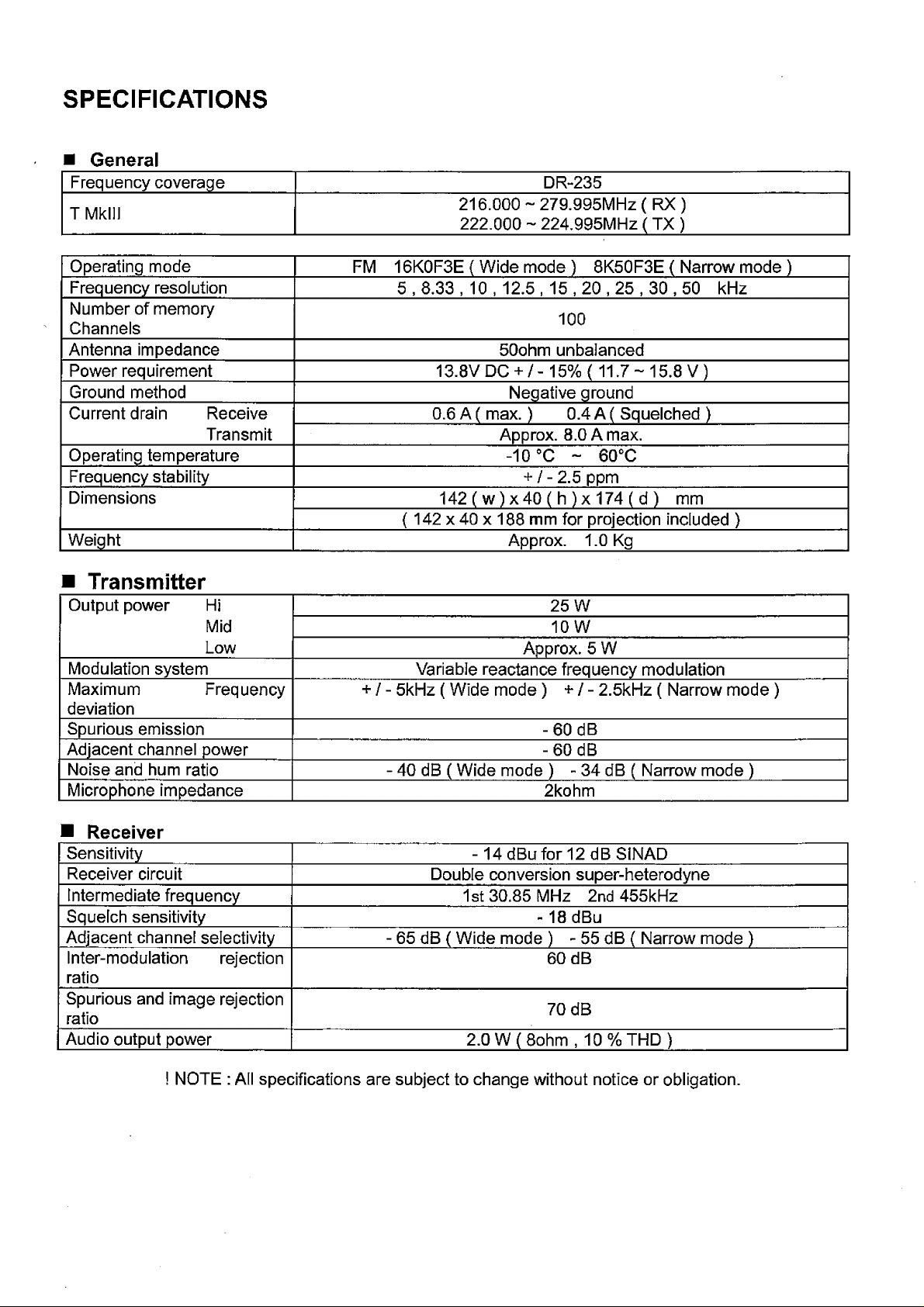
SPECIFICATIONS
■ General
Frequency coverage
TMklll
DR-235
216.000 ~ 279.995MHz ( RX )
222.000 - 224.995MHz ( TX )
Operating mode
Frequency resolution
Number of memory
Channels
Antenna impedance
Power requirement
Ground method
Current drain Receive
Transmit
Operating temperature
Frequency stability
Dimensions
Weight Approx. 1.0 Kg
FM 16K0F3E ( Wide mode ) 8K50F3E ( Narrow mode )
5 , 8.33 , 10 , 12.5 , 15 , 20 , 25 , 30 , 50 kHz
100
50ohm unbalanced
13.8V DC + / - 15% ( 11.7 ~ 15.8 V )
Negative ground
0.6 A ( max.) 0.4 A ( Squelched )
Approx. 8.0 A max.
-10 °C - 60°C
+ / - 2.5 ppm
142 ( w ) x 40 ( h ) x 174 ( d ) mm
( 142 x 40 x 188 mm for projection included )
■ Transmitter
Output power Hi
Mid
Low
Modulation system
Maximum Frequency
deviation
Spurious emission -6 0 dB
Adjacent channel power
Noise and hum ratio
Microphone impedance
+ / - 5kHz ( Wide mode ) + / - 2.5kHz ( Narrow mode )
Variable reactance frequency modulation
- 40 dB ( Wide mode ) - 34 dB ( Narrow mode )
25 W
10 W
Approx. 5 W
-6 0 dB
2kohm
■ Receiver
Sensitivity
Receiver circuit
Intermediate frequency
Squelch sensitivity
Adjacent channel selectivity
Inter-modulation rejection
ratio
Spurious and image rejection
ratio
Audio output power
! NOTE : All specifications are subject to change without notice or obligation.
-14 dBu for 12 dB SINAD
Double conversion super-heterodyne
1st 30.85 MHz 2nd 455kHz
-1 8dBu
- 65 dB ( Wide mode ) - 55 dB ( Narrow mode )
60 dB
70 dB
2.0 W ( 8ohm , 10%THD )
Page 3
CIRCUIT DESCRIPTION
1) R e c e iv e r S y s te m D R - 2 3 5
The receiver system is a double superheterodyne system with a 30.85 MHz first IF and a 455 kHz
second IF.
1. Front End
2. IF Circuit
3. Demodulation Circuit
The received signal at any frequency in the 216.000MHz to 279.995MHz
range is passed through the low-pass filter (L116, L115, L114, L113, C204,
C203, C202, C216 and C215) and tuning circuit (L105, L104 and D105,
D104), and amplified by the RF amplifier (Q107). The signal from Q107 is
then passed through the tuning circuit (LI 03, L107, L102, and varicaps
D103, D107 and D102) and converted into 30.85 MHz by the mixer
(Q106). The tuning circuit, which consists of L105, L104, varicaps D105
and D104, L103, L107, L102, varicaps D103, D107 and D102, is
controlled by the tracking voltage form the VCO. The local signal from the
VCO is passed through the buffer (Q145), and supplied to the source of
the mixer (Q106). The radio uses the lower side of the superheterodyne
system.
The mixer mixes the received signal with the local signal to obtain the sum
of and difference between them. The crystal filter (XF101A, XF101B)
selects 30.85 MHz frequency from the results and eliminates the signals
of the unwanted frequencies. The first IF amplifier (Q105) then amplifies
the signal of the selected frequency.
After the signal is amplified by the first IF amplifier (Q105), it is input to pin
16 of the demodulator IC (IC108). The second local signal of 30.395 M Hz,
which is oscillated by the internal oscillation circuit in 1C108 and crystal
(X104), is input through pin 1 of 1C108. Then, these two signals are mixed
by the internal mixer in IC108 and the result is converted into the second
IF signal with a frequency of 455 kHz. The second IF signal is output from
pin 3 of IC108 to the ceramic filter (FL101 or FL102), where the unwanted
frequency band of that signal is eliminated, and the resulting signal is sent
back to the IC108 through pins 5.
The second IF signal input via pin 5 is demodulated by the internal limiter
amplifier and quadrature detection circuit in IC108, and output as an audio
signal through pin 9.
4. Audio Circuit
The audio signal from pin 9 of IC108 is amplified by the audio amplifier
(IC120:A),and switched by the signal switch IC (IC111) and then input it to
the de-emphasis circuit.
and is compensated to the audio frequency characteristics in the
de-emphasis circuit (R203, R207, R213, R209, C191, C218, C217) and
amplified by the AF amplifier (IC120:B). The signal is then input to volume
(VR1) . The adjusted signal is sent to the audio power amplifier (IC117)
through pin 1 to drive the speaker.
Page 4
5. Squelch Circuit
The detected output which is outputted from the pin 9 of IC108 is inputted
to pin 8 of IC108 after it was been amplified by 10120:A and it is outputted
from pin 14 after the noise component was been eliminated from the
composed band pass filter in the built in amplifier of the IC. The adjusted
voltage level at VR101 is delivered to the comparator of the CPU.
The voltage is led to pin 2 of CPU and compared with the setting voltage.
The squelch will open if the input voltage is lower than the setting voltage.
During open squelch, pin 30 (SQC) of the CPU becomes "L" level, AF
control signal is being controlled and sounds is outputted from the
speaker.)
6. AIR Band Reception
If it is made air band receiving mode, IF signal is demodulated by AM
decoder of IC108, and is output from pin12 as the AF signal.
7. WIDE/NARROW
Switching circuit
2) T ra n s m itte r S y s te m D R - 2 3 5
The 2nd IF 455 kHz signal which passes through filter FL101 (wide) and
FL102 (narrow) during narrow, changes its width using the width control
switching D115 and D116.
1. Modulator Circuit
The audio signal is converted to an electrical signal by the microphone,
and input it to the microphone amplifier (Q6). Amplified signal which
passes through mic-mute control IC109 is adjusted to an appropriate
mic-volume by means of mic-gain adjust VR106.
IC114:C and D consists of four operational amplifiers; one amplifier (pins
12, 13, and 14) is composed of pre-emphasis and IDC circuits and the
other (pins 8, 9, and 10) is composed of a splatter filter. The maximum
frequency deviation is obtained by VR107. and input to the signal switch
(IC113) (9600 bps packet signal input switch) and input to the cathode of
the varicap of the VCO, to change the electric capacity in the oscillation
circuit. This produces the frequency modulation.
2. Power Amplifier Circuit
3. APC Circuit
The transmitted signal is oscillated by the VCO, amplified by the drive
amplifier (Q145) and younger amplifier (Q115), and input to the final
power module (IC110). The signal is then amplified by the final power
module (IC110) and led to the antenna switch (D110) and low-pass filter
(L113, L114, L115, L116, C215, C216, C202, C203 and C204), where
unwanted high harmonic waves are reduced as needed, and the resulting
signal is supplied to the antenna.
Part of the transmission power from the low-pass filter is detected by
D111, converted to DC. The detection voltage is passed through the APC
circuit (IC114:A,IC114:B), then it controls the APC voltage supplied to the
younger amplifier Q115 and the final power module IC110 to fix the
transmission power.
Page 5
3) PLL Synthesizer Circuit DR- 235
1. PLL
The dividing ratio is obtained by sending data from the CPU (IC1) to pin 10
and sending clock pulses to pin 9 of the PLL IC (IC116). The oscillated
signal from the VCO is amplified by the buffer (Q134 and Q135) and input
to pin 8 of IC116. Each programmable divider in IC116 divides the
frequency of the input signal by N according to the frequency data, to
generate a comparison frequency of 5 or 6.25 kHz.
2. Reference Frequency
Circuit e re^erence frequency appropriate for the channel steps is obtained by
dividing the 12.8 MHz reference oscillation (X102) by 4250 or 3400,
according to the data from the CPU (IC1). When the resulting frequency is
5 kHz, channel steps of 5, 10,15, 20, 25, 30, and 50 kHz are used. When
it is 6.25 kHz, the 12.5 kHz channel step is used.
3. Phase Comparator Circuit
The PLL (IC116) uses the reference frequency, 5 or 6.25kHz. The phase
comparator in the IC116 compares the phase of the frequency from the
VCO with that of the comparison frequency, 5 or 6.25kHz, which is
obtained by the internal divider in IC116.
4. PLL Loop Filter Circuit
If a phase difference is found in the phase comparison between the
reference frequency and VCO output frequency, the charge pump output
(pin 5) of IC116 generates a pulse signal, which is converted to DC
voltage by the PLL loop filter and input to the varicap of the VCO unit for
oscillation frequency control.
5. VCO Circuit
A Colpitts oscillation circuit driven by Q131 directly oscillates the desired
frequency. The frequency control voltage determined in the CPU (IC1) and
PLL circuit is input to the varicaps (D122 and D123). This change the
oscillation frequency, which is amplified by the VCO buffer (Q134) and
output from the VCO area.
4) C P U a n d P e rip h e r a l C irc u its
1. LCD Display Circuit
The CPU turns ON the LCD via segment and common terminals with 1/4
the duty and 1/3 the bias, at the frame frequency is 64Hz.
2. Dimmer Circuit
3. Reset and Backup
The dimmer circuit makes the output of pin 13 of CPU (IC1) into "H" level
at set mode, so that Q9 and Q3 will turn ON to make the lamp control
resistor R84 short and make its illumination bright. But on the other hand,
if the dimmer circuit makes pin 13 into "L" level, Q9 and Q3 will turn OFF,
R84's illumination will become dimmer as its hang on voltage falls down in
the working LED (D11, D2, D5, D3 and D6).
When the power form the DC cable increases from Circuits 0 V to 2.5 or
more, "H" level reset signal is output form the reset IC (IC4) to pin 33 of
the CPU (IC1), causing the CPU to reset. The reset signal, however, waits
at 100, and does not enter the CPU until the CPU clock (X1) has
stabilized.
Page 6
4. S (Signal) Meter Circuit
The DC potential of pin 12 of iC108 is input to pin 1 of the CPU (IC1),
converted from an analog to a digital signal, and displayed as the S-meter
signal on the LCD.
5. DTMF Encoder
6. Tone Encoder
7. DCS Encoder
8. CTCSS, DCS Decoder
The CPU (IC1) is equipped with an internal DTMF encoder. The DTMF
signal is output from pin 10, through R35, R34 and R261 (for level
adjustment), and then through the microphone amplifier (IC114:D), and is
sent to the varicap of the VCO for modulation. At the same time, the
monitoring tone passes through the AF circuit and is output form the
speaker.
The CPU (IC1) is equipped with an internal tone encoder. The tone signal
(67.0 to 250.3 Hz) is output from pin 9 of the CPU to the varicap (D120) of
the VCO for modulation.
The CPU (IC1) is equipped with an internal DCS code encoder. The
code (023 to 754) is output from pin 9 of the CPU to the PLL reference
oscillator. When DCS is ON, DCS MUTE circuit (Q126-ON, Q133-ON,
Q132-OFF) works. The modulation activates in X102 side only.
The voice band of the AF output signal from pin 3 of IC120:A is cut by
sharp active fitter IC104:A and D (VCVS) and amplified, then ied to pin 4
of CPU. The input signal is compared with the programmed tone
frequency code in the CPU. The squelch will open when they match.
During DCS, Q108 is ON, C419 is working and cut off frequency is
lowered.
5) P o w e r S u p p ly C ir c u it
When power supply is ON, there is a "L" signal being inputted to pin 39 (PSW) of CPU which enables the CPU to
work. Then, "H" signal is outputted from the pin 41 (C5C) of CPU and drives ON the power supply switch control
Q8 and Q7 which turns the 5VS ON.5VS turns ON the PLL IC116, main power supply switch Q127 and Q122, AF
POWER IC117 and the 8 V of AVR (IC115).During reception, pin 29 (R5) of CPU outputs "H" level, Q124 is ON,
and the reception circuits supplied by 8 V.While during transmission, pin 28 (T5) of CPU outputs "L" level which is
reverse by Q11 so that the output in Q128 will be "H" level, Q123 is ON, and the transmission circuit is supplied by
8 V.Or, in the case when the condition of PLL is UNLOCK, "L" level is outputted from pin 14 of IC116, UNLOCK
switch Q148 is OFF,Q129is ON, transmission switch Q128 is OFF which makes the transmission to stop.
1. ACC External Power Supply Terminal
When optional power supply cord DEC-37 etc. is connected to the
external power supply terminal JK101, with ACC power supply ON, switch
Q101 will turn ON, 5 V of AVR IC101 pin 2 (STB) becomes "L" which
makes C5V to turn ON. With this, it can turn the power supply of the radio
ON.
Page 7
P67/AN7-
P66/AN6-
P65/AN5-
P64/AN4-
P63/SCLK22/AN3-
P62/SCLK21/AN2-
P61/S0UT2/AN1 -
P60/SIN2/AN0-
P57/ADT/DA2-
P56/DA1 *
P55/CNTR1 -
P54/CNTR0-
P53/RTP1-
P52/RTP0-
P51/PWM1-
P50/PWM0-
P47/5EÜYT-
P46/SCLK1-
P45/TXD-
P44/RXD-
P43/sjS/T0UT ■
P42/INT2-
P41/INT1-
P40-
P77-
< <c <oo<Z50<^ 3<m mrnm rn m m rnm m cr>oo
i v~^ c~ ¿ i i s i s * â ■ c/o r n ç ? C5 ij ^ b~ ^ l~ ? c? ü i <r> * * * *
-» -‘ P O i\)w o -*ro w M T io o -‘ pow^üio>H oo(oo-áro
o o o o > < c^ c^co coc /5c <o< />o oc^o om mm
ililiîîîîil ÎÎÎÎÎÎIÎÎÎÎÎÎ
O
= o
o o
o o
r o
o >
o o
S
< r >
i—
o
OO
OO
C D
" O
'ñ
■M
s '
---
-X
44=
f ~
O
O
GO <SÎ C/O
SEG13
SEG14
SEG15
SEG16
SEG17
P30/SEG18
P31/SEG19
P32/SEG20
P33/SEG21
P34/SEG22
P35/SEG23
P36/SEG24
P37/SEG25
P00/SEG26
P01/SEG27
P02/SEG28
•P03/SEG29
P04/SEG30
■P05/SEG31
•P06/SEG32
■PÛ7/SEG33
•P10/SEG34
•P11/SEG35
■P12/SEG36
■ P13/SEG37
O
T I
<
m
5*
3
M
O
O
3
CD
§.
O
ZD
O
T I
C
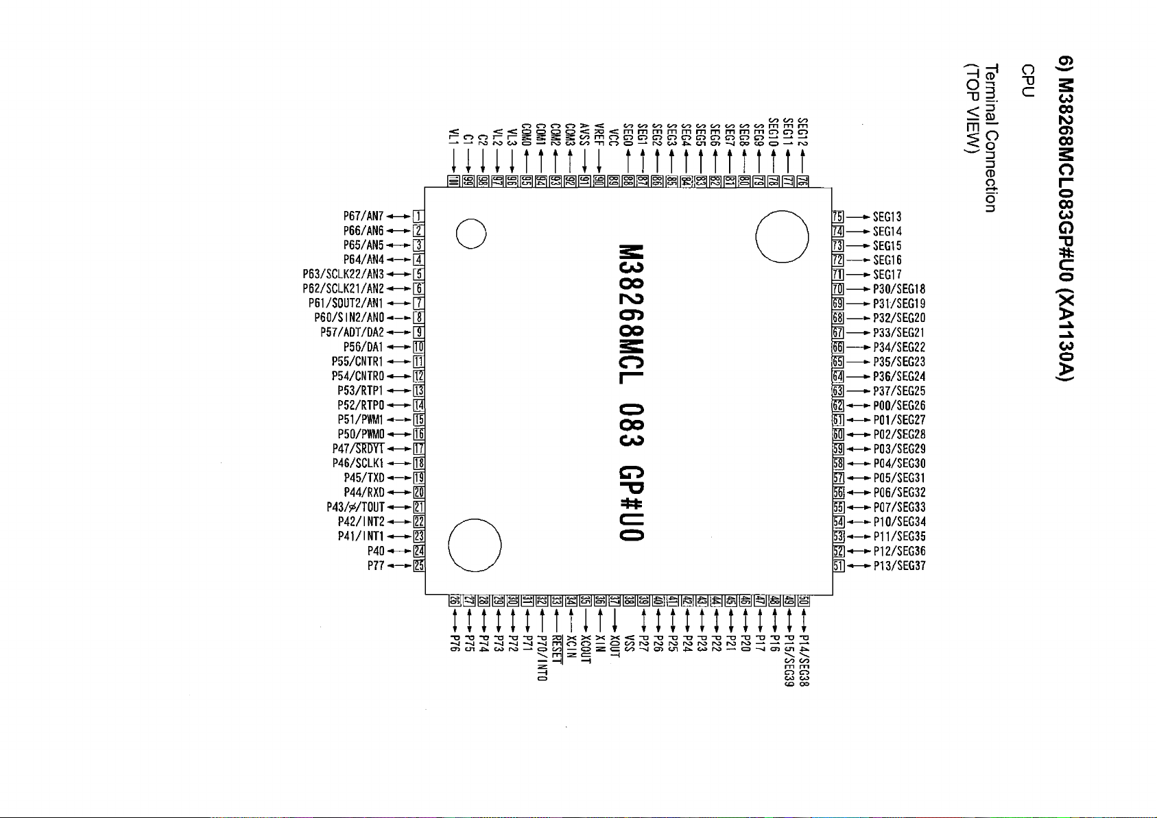
6) M 38 2 6 8 M C L 0 8 3 G P # U 0 (X A 1 1 3 0 A )
n n n m i í i m n n n n t
■0-0-0‘T3*U‘T3*TD^|XXX X<"0-D_a-D"0_0'T3'I3T3'D'DT1
—* O CTJ CJÏ -ÍX
C"5 CT5
CO to
CO oo
Page 8
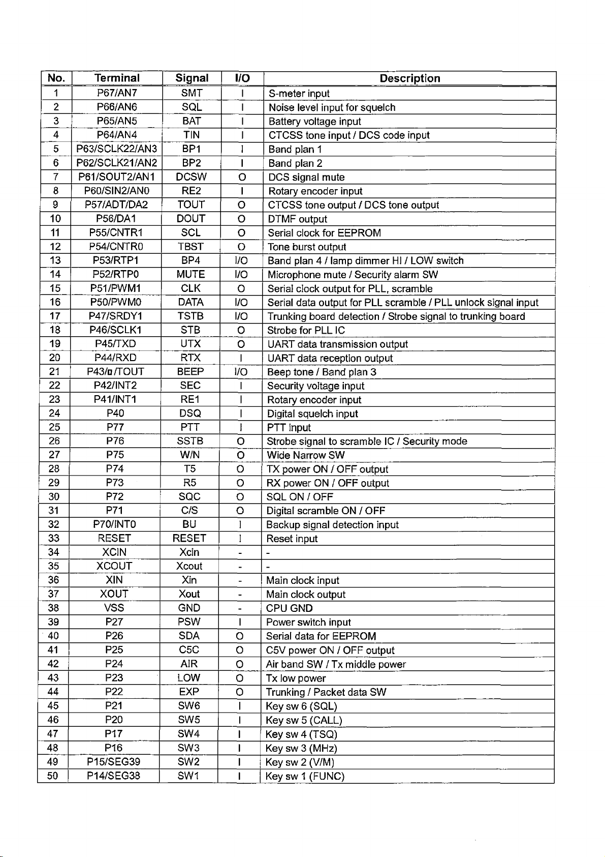
No. Terminal Signal
1 P67/AN7
2
3
4
P66/AN6 SQL I
P65/AN5 BAT I
P64/AN4
5 P63/SCLK22/AN3
SMT
TIN
BP1
6 P62/SCLK21/AN2 BP2
7 P61/SOUT2/AN1 DCSW
8 P60/SIN2/AN0 RE2
9 P57/ADT/DA2 TOUT
10 P56/DA1 DOUT
11 P55/CNTR1 SCL
12 P54/CNTR0 TBST
13 P53/RTP1 BP4
14 P52/RTP0 MUTE
15 P51/PWM1 CLK
16 P50/PWM0 DATA
17 P47/SRDY1 TSTB
18 P46/SCLK1 STB
19 P45/TXD UTX
20 P44/RXD
RTX
21 P43/n/TOUT BEEP
22 P42/INT2 SEC
23 P41/INT1 RE1
24 P40 DSQ
25 P77 PTT
26 P76
SSTB
27 P75 W/N
28 P74 T5
29 P73 R5
30 P72 SQC
31 P71 C/S
32 P70/INT0 BU
33 RESET RESET
34 XCIN Xcin
35 XCOUT Xcout
36 XIN Xin
37 XOUT Xout
38 VSS GND
39 P27 PSW
40 P26 SDA
41 P25 C5C
42 P24 AIR
43
44
P23 LOW
P22
EXP
45 P21 SW6
46 P20 SW5
47 P17 SW4
48 P16 SW3
49 P15/SEG39 SW2
50 P14/SEG38 SW1
I/O Description
I
S-meter input
Noise level input for squelch
Battery voltage input
I CTCSS tone input / DCS code input
I Band plan 1
I Band plan 2
0 DCS signal mute
I Rotary encoder input
0 CTCSS tone output / DCS tone output
0 DTMF output
0 Serial clock for EEPROM
0
Tone burst output
I/O Band plan 4 / lamp dimmer HI / LOW switch
I/O Microphone mute / Security alarm SW
O Serial clock output for PLL, scramble
I/O Serial data output for PLL scramble / PLL unlock signal input
I/O Trunking board detection / Strobe signal to trunking board
0 Strobe for PLL IC
UART data transmission output
0
I UART data reception output
I/O Beep tone / Band plan 3
I Security voltage input
I Rotary encoder input
I Digital squelch input
I PTT input
0 Strobe signal to scramble IC / Security mode
Wide Narrow SW
0
0
TX power ON / OFF output
0
RX power ON / OFF output
o SQL ON / OFF
o Digital scramble ON / OFF
I Backup signal detection input
I Reset input
- -
- -
-
Main clock input
-
Main clock output
-
CPU GND
I Power switch input
o
0 C5V power ON / OFF output
0 Air band SW / Tx middle power
0 Tx low power
0 Trunking / Packet data SW
Serial data for EEPROM
I Key sw 6 (SQL)
I Key sw 5 (CALL)
I Key sw 4 (TSQ)
I Key sw 3 (MHz)
I Key sw 2 (V/M)
Key sw 1 (FUNC)
Page 9
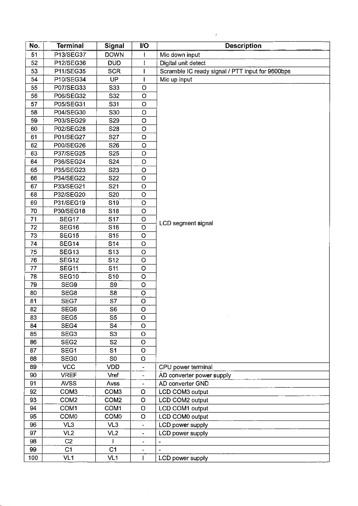
No. Terminal Signal I/O Description
51
52
P13/SEG37
DOWN I Mic down input
P12/SEG36 DUD I Digital unit detect
53 P11/SEG35 SCR I Scramble IC ready signal / PTT input for 9600bps
54 P10/SEG34 UP I Mic up input
55 P07/SEG33 S33 0
56 P06/SEG32 S32 0
57 P05/SEG31 S31 0
58 P04/SEG30 S30
59 P03/SEG29 S29
60 P02/SEG28
S28 0
61 P01/SEG27 S27
62
P00/S EG26 S26 0
0
0
0
63 P37/SEG25 S25 0
64 P36/SEG24 S24 0
65 P35/SEG23
S23 0
66 P34/SEG22 S22 0
67 P33/SEG21 S21 0
68 P32/SEG20 S20 0
69
P31/SEG19 S19 0
70 P30/SEG18 S18 0
71
72
73 SEG15 S15
SEG17
SEG16
S17
S16
0
LCD segment signal
0
0
74 SEG14 S14 0
75 SEG13 S13 0
76 SEG12 S12 0
77
78
79 SEG9
80 SEG8 S8
81 SEG7 S7
82 SEG6 S6
SEG11 S11 0
SEG10 S10 0
S9 0
0
0
0
83 SEG5 S5 0
84 SEG4 S4 0
85 SEG3 S3 0
86 SEG2 S2 0
87 SEG1 S1 0
88 SEGO SO 0
89 VCC VDD
90 VREF Vref
91 AVSS Avss -
92
COM3 COM3 0 LCD COM3 output
-
CPU power terminal
-
AD converter power supply
AD converter GND
93 COM2 COM2 0 LCD COM2 output
94 COM1 COM1 0 LCD COM1 output
95 COMO COMO
96 VL3 VL3 -
97 VL2 VL2
98 C2 I
99 C1 C1
100 VL1 VL1
0
LCD COMO output
LCD power supply
LCD power supply
- -
- -
I LCD power supply
Page 10
SEMICONDUCTOR DATA
1) N J M 7 8 0 8 F A (X A 0 1 0 2 )
8V (1A) Voltage Regulator
O
7808A
J RC
******
1. INPUT
2. COMMON
3. OUTPUT
1 2 3
2 ) T C 4 S 6 6 F (X A 0 1 1 5 )
Bilateral Switch
5 4
b
_____
a
C 9
□
1
3 ) A N 8 0 1 0 M (X A 0 1 1 9 )
10V (50mA) Voltage Regulator
1. IN/OUT
2. O UT/IN
3. VSS
4. CONT
5. VDD
J^L
a
□ □ t j
1 2 3
Vin
CONT
Function (IN-OUT)
Disconnect (Hi Z)
L
H Connect (290ohm typ.)
•c
C_3
u u
1 2
**
Ü
3
1. OUTPUT
2. COMMON 1
3. INPUT
4 ) T C 4 W 5 3 F U (X A 0 3 4 8 )
Multiplexer / De-multiplexer
8 7 6 5
n p
1. COMMON
2. INH
3. VEE
4. VSS
5. A
6. ch 1
7. ch 0
8. VDD
i-L
’ T
0
------
• —
GND
1
K
S
S
Control
INH
L
L
H
* Don’t’t care
Shari circuit
pro to lor
input
A
L
H
*
3
Vaut
ON channel
ch 0
ch 1
NONE
Page 11
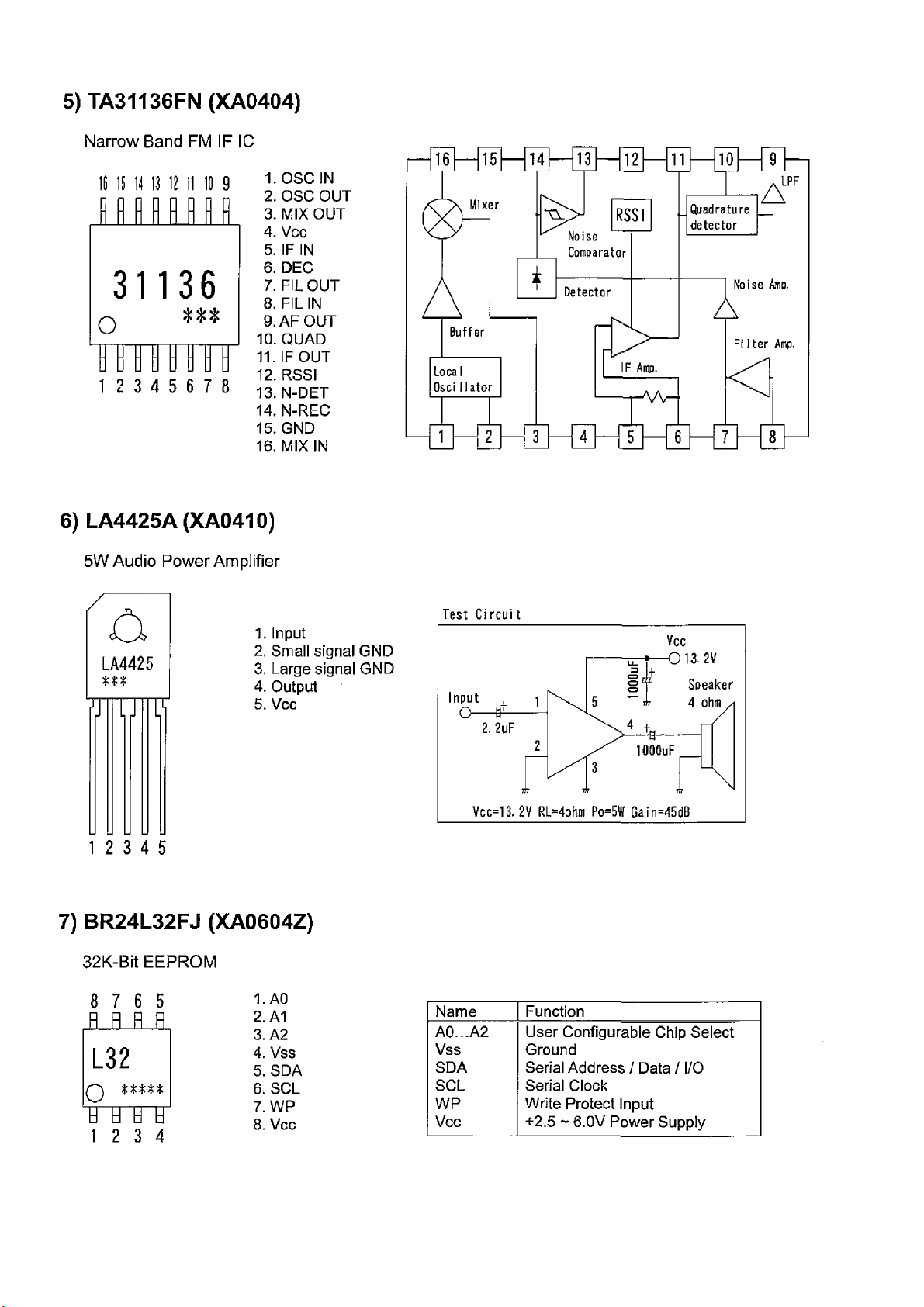
5) TA31136FN (XA0404)
Narrow Band FM IF IC
It 15 14 13 12 11 10 9
3
1136
o
n
1 2 3 4 5 6 7 8
6) L A 4 4 2 5 A (X A 0 4 1 0 )
1.
2.
3. MIX OUT
4.
Vcc
5.
6. DEC
7.
8. FILIN
9.AF OUT
10. QUAD
11. IF OUT
12. RSSI
13. N-DET
14. N-REC
15. GND
16. MIX IN
OSCIN
OSC OUT
IF IN
FILOUT
5W Audio Power Amplifier
¿X
LA4425
***
WILJIIUi
1. Input
2. Small signal GND
3. Large signal GND
4. Output
5. Vcc
1 2 3 4 5
7) B R 2 4 L 3 2 F J (X A 0 6 0 4 Z )
32K-Bit EEPROM
8 7 6 5
R R R R
1. AO
2. A1
3. A2
4. Vss
5. SDA
6. SCL
7. WP
8. Vcc
Test Circuit
Name Function
A0...A2
Vss
SDA
SCL
WP
Vcc
User Configurable Chip Select
Ground
Serial Address / Data / I/O
Serial Clock
Write Protect Input
+2.5 ~ 6.0V Power Supply
Page 12
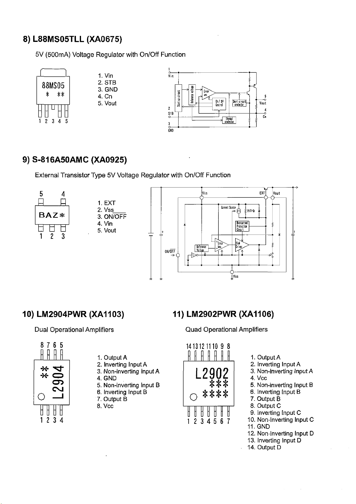
8) L88MS05TLL (XA0675)
5V (500mA) Voltage Regulator with On/Off Function
I
------------
1 2 3 4 5
9) S -8 1 6 A 5 0 A M C (X A 0 9 2 5 )
External Transistor Type 5V Voltage Regulator with On/Off Function
1
1. Vin
2. STB
3. GND
4. Cn
5. Vout
GND
5
p
B A Z *
B d d
f l
4
1. EXT
2. Vss
3. ON/OFF
4. Vin
5. Vout
1 2 3
1 0 ) L M 2 9 0 4 P W R (X A 1 1 0 3 )
Dual Operational Amplifiers
8 7 6 5
1. Output A
2. Inverting Input A
3. Non-inverting Input A
4. GND
5. Non-inverting Input B
6. Inverting Input B
7. Output B
8. Vcc
o
CD
cn
CVJ
—1
12 3 4
11 ) L M 2 9 0 2 P W R ( X A 1 1 0 6 )
Quad Operational Amplifiers
1. Output A
2. Inverting Input A
3. Non-Inverting Input A
4. Vcc
5. Non-inverting Input B
6. Inverting Input B
7. Output B
8. Output C
9. Inverting Input C
2 3 4 5 6 7
10. Non-inverting Input C
11. GND
12. Non-Inverting Input D
13. Inverting Input D
14. Output D
Page 13

12) MB15E07SR (XA1107)
PLL Synthesizer
16 15 14 13 12 11 10 9
OSC IN
PS
IE
Data
Clock
Xfin
fin
Reference
Oscillator
lot errait tent
mode control
(porer save)
l-bit
control latch
Prescaler
32/33
64/65
Binary I4-bit
rcfcrcncc counter
14-bit latch
SW
1. OSC IN
2. N. C.
3. Vp
4. Vcc
5. Do
6. GND
7. Xfin
8. fin
Sff FC LDS CS
4-bit latch
19-bit shift register
7-bit latch 11-bit latch
Binaly 7-bit
swallow
counter
Binary 11-bit
programmable
counter
9. Clock
10. Data
11. LE
12. PS
13.N.C.
14. LD/fout
15.N.C.
16.N.C.
ÍP
fr
Phase
comparator
Lock
dctcctor
LD/fr/fp
selector
Charge pump
■LD/fout
Vp
Do
VCC
GND
Parameter
Symbo
I
Power supply voltage Vcc
Power supply current
LPF supply voltage
icc
Vp
Local oscillator input level Vf in
Local oscillator input
frequency
Xin input level
fin
Vxin
Xin input frequency Fxin
( Vcc = 2.7 to 5.0V, Ta = -40°C to +85oC )
Condition Min. Typ.
-
2500MHz
Vcc=Vp=3.75V
-
100MHz to 300MHz
300MHz to 2500MHz
-
-
-
Max. Unit
2.7 3.75 5.0
8.0
Vcc
-6
-15
-
5.5 V
+2
+2
100 2500
0.5
3
Vcc
40
V
mA
dBm
MHz
Vp-p
MHz
Page 14

13) S-80845CLNB (XA1120)
4.5V Voltage Detector
4 3
1. Vout
2. Vin
3. NC
4. GND
1 4 ) B U 4 0 5 2 B F V (X A 1 2 2 9 )
Analog Multiplexer / De-multiplexer
YO (T
Y2 [T -
Y COMMON [T -
Y3 [7 -
Y1 \T - Y1 xo
INHIBIT (T -
- VEE B
VEE [T
VSS [T
I
Y2 VO
Y
IN/OUT
vs X
U IN/OUT
INH
I
if] VDD
X2 -
15] X2
XI - J4] XI
-
35 X COMMON
3U XO
-
X3
W] X3
A-To] A
T] B
INHIBIT A B COMMON ON SWITCH
L L L
L H
L L H X2 Y2
L
X Y
XO YO
X1 Y1
L H H X3 Y3
*
H
*
NONE
* Don’t care
Page 15

15) S-AV40 (XA1230)
222 ~ 225MHz 30W RF Power Module
BLOCK DIAGRAM
G H b
® RF Input (Pin)
(D Gate Voltage (VGG), Power Control
® Drain Voltage (VDD), Battery
(D RF Output (Pout)
© RF Ground (Frange)
ABSOLUTE MAXIMUM RATING ( Tc = 25 °C, unless otherwise noted )
Symbol
VDD
VGG Gate Voltage
IDD Drain Current 8 A
Pin
Pout
Tease (OP)
Tstg Storage Temprature -40 to +110 °C
Drain Voltage VGG < 5V, Pi = 50mW, Po < 30W 17
Input Power 12.5V < VDD < 16.5V, VGG = 5V,
Output Power 30
Operation Case Temperature -30 to +100
Parameter Conditions
VDD < 12.5V, Pin=50mW
Pi = 50 mW
Ratings Unit
6 V
100
ELECTRICAL CHARACTERISTICS ( Tc = 25°C, unless otherwise noted )
Symbol Parameter Conditions
f
Pout Output Power
V T
2fo 2na Harmonic -25 dBc
Pin
IGG
-
-
Frequency Range
Total Efficiency
Input VSWR
Gate Current
Stability VDD=10.5-16,5V, VGG=0-5V, Pin=50mW,
Load VSWR
Tolerance
VDD = 12.5V
VGG = 5V
Pin = 50mW
Pout<30W (VGG control),
Load VSWR=3:1 ALL PHASE
VDD=15.0V, Pin=50mW,
Pout=30W (VGG control),
Load VSWR=10:1 ALL PHASE
All sprious output
than 60dB bellow
desired signal
Ratings
Min Typ Max
220
30 W
40 %
No degradation
246 MHz
1 mA
3.0
V
mW
W
°C
Unit
-
-
Page 16

1 6 ) T ra n s is to r, D io d e a n d L E D O u tlin e D ra w in g
Top View
MI 407
XDÓÓÍ3
ÍH 3
S
MA2S111
XD0323
VDZ5. 1B
XDÖ4Ö2 "
i
DA204U
XDÓÍ3Ó
K
n— u
JL
«
RLS—73
XD0363
Q O
S3V60
XDÖ414
Œ
1SV237
XD0Í4Í
BB
ta
1SV278
XDÍ3374
RB521S
XD04Í8
RN731V
XDÔ25T
MA4S713
"XDO’3’75"
n n
MIN
n ~ n
n .□
n ~n
015AZ3- 0
’’XD045Í"
4 M
:
1SV268
XDÔ3ÔÎ
i—i
i n ru
i i
A r
1SV282
XD0376
2SK880GR
XËÔÔ2Δ
XG
MA2S728
XD0315 "
t u
CRG01
XD039Í
I gD
3SK293
XÉd053
G2 Gl
B
___
Q
UF
b n
D S
DAN235E
XDÖ32Ö"
H----CT
_Q
TT
m— er
UDZS5. 6B
XD0395*
4 D
2SK2539
XËÔ066 ~
AK*
FA1111C
XLÖÖ69 ”
2SC5551
~xf0194
U U U
B C E
RN2107FV
XÚ02ÍÍ"
c
__□__
YH
u u
B E
FA1111C
XLÔÔ77 "
2SD2620J
"xf0208 ~
3B
2SA1036K
" x fö iiö "
c
n
HQ
2SC6026MFV
""xfÖ2l"Ö"~
HG
2SC4245Y
” xfdÍ25~'
HB
XP1215
XÙ0178
9M
Rb=1Okohm
Rbe=none
2SB766A
m m
BOR
u u u
B C E
RN1104
XÙÔ195
XD
n— e r
Rb=47kohm
Rbe=47kohm
2SC4915
~xf Ö Í 78 ~
QO
EMD6
XÛÔ2Ô9
O CD LU
r» n n
D6
Rb=4. 7kohm
Rbe=none
2SB1386
xf0190 "
BHQ
U U ü
B C E
RN1107FV
XÜ02Í0"
XH
n— u
Rb=1Okohm
Rbe=47kohm
Rb=lOkohm
Rbe=47kohm
Page 17

V
Page 18

Íez
f e
17) LCD C on n ection (T T R 3 6 2 6 U P F D H N )
O
O
COM3
CO M 2
C0M 1
COMO
ei
Page 19

EXPLODED VIEW
1) LCD Assembly
FF0017
ST 0 0 6 4
Page 20

2) Top and Front View
AA0050
DP0185
‘ NK0072 KZ01D5
NK0073
Page 21

3 ) B o tto m V ie w
AA0050
Page 22

PARTS LIST
CPU Unit
Part No.
Ref No
C1 CU3554 Chip C.
C2
CU3554
C3
CU3549 Chip C.
C4 CU3549 Chip C.
C5 CU3554 Chip C.
C6
CU3523
CU3523
C7
CS CU3543 Chip C.
CU3554
C9
C10 CU3543 Chip C. GRM155B11E472KA01D
C11 CU3543 Chip C.
CU3553
C12
C13 CS0049 Chip tantalum TMCSA1C105MTRF 1
C14 CU3514 Chip C.
CU3514
C15
C16 CU3535 Chip C. GRM155B11H102KAD1D
C17 CS0424 Chip tantalum
CU3535
C18
C19 CU3554 Chip C.
C20 CU3547 Chip C.
C21
CU3547
022 CU3535 Chip C.
C23 CU3547 Chip C.
C24 CU3535
C25 CU3535 Chip C.
C26 CU3535 Chip C.
C27 CU3535 Chip C. GRM155B11H102KA01D
C28 CS0439 Chip tantalum
C29 CSD049
C30 CS0424 Chip tantalum
CU3547
C31
C32 CU3547 Chip C.
CN1 UE0291 Connector
CN2 UE0291
CN3 UE0035Z Mic Connector
D1
XL0069 Chip LED
D2 XL0077 Chip LED
D3 XL0077 Chip LED
XL0069
D4
D5 XL0077 Chip LED
XL0077
D6
D8 XD0323 Chip Diode
D9 XD0418 Chip Diode
D10 XDD391 Chip Diode
D11 XL0077 Chip LED
XDD402
D12
D13 XD0402 Chip Diode
D14
XD0418 Chip Diode
D15 XD0402
D16 XD0418 Chip Diode
D17
XD0418
D19 XD0363 Chip Diode
IC1 XA1130A IC
IC2 XA06D4Z IC BR24L32FJ-WE2 1
IC4 XA1120 IC
IC5 XA0675 IC
JK1 UJ0047 Jack HSJ2013-01-120 1
JP3 MACL04GG W ire
LGD1 EL0049 LCD
XUD210 Chip Transistor RN1107MFV(TPL3) 1
Q1
Q2 XU0210 Chip Transistor
Q3 XT0110 Chip Transistor
Q4 XUD210
Q5 XU0210 Chip Transistor
Q6 XT0210 Chip Transistor
Q7
XTD170 ChipTransistor
Q6 XUÛ210 Chip Transistor
Q9 XU0195 Chip Transistor
Q10 XU0210 Chip Transistor
XU0211 Chip Transistor
Q11
Q12 XU0211 Chip Transistor RN21Q7MFV{TPL3)
Q13 XU0211 Chip Transistor
R1 RK3554 Chip R.
R2 RK3501 Chip R. ERJ2GE0R0DX 1
R4 RK3554 Chip R.
R5 RK3S50 Chip R.
R6 RK3550 Chip R.
R7 RK0025
R8 RK0025 Chip R.
R9 RK3538 Chip R.
R10 RK3032 Chip R.
R11 RK3546 Chip R.
R14 RK3548 Chip R.
R16 RK3001 Chip R. MCR03EZPJ0Û0 1
R19 RK3562 Chip R.
R20 RK3542 Chip R.
R21 RK3030 Chip R.
Description
Chip C.
Chip C.
Chip C.
Chip C.
Chip C.
Chip C.
Chip C.
Chip C.
Chip C.
Chip tantalum TMCSA1C105MTRF
Chip C.
Connector
Chip LED FA1111C-TR 1
Chip LED FA1111C-732-TR
Chip Diode VDZT2R 5.1 B
Chip Diode VDZT2R 5.1 B
Chip Diode
Chip Transistor
Chip R. ERJ6GEYJ331V 1
Parts Name Qty.
GRM155B11A104KA01D 1
GRM155B11A104KA01D 1
GRM155B11C153KA01D 1
GRM155B11C153KA01D 1
GRM155B11A104KA01D 1
GRM1552C1H101JD01D
GRM1552C1H101JD01D
GRM15ÖB11E472KA01D 1
GRM155B11A104KA01D 1
GRM155B11E472KA01D 1
GRM155B11A473KA01D 1
GRM1552C1H18DJZ01D 1
GRM1552C1H180JZ01D 1
TMCMA1C1Û6MTRF
GRM155B11H102KA01D 1
GRM155B11A104KA01D
GRM155B11C103KA01D 1
GRM155B11C103KA01D 1
GRM155B11H102KA01D
GRM155B11C103KA01D 1
GRM155B11H102KA01D 1
GRM155B11H102KAD1D 1
GRM155B11H102KA01D 1
TMCMA0J476MTRF 1
TMCMA1C106MTRF
GRM155B11C103KA01D 1
GRM155B11C103KAO1D
17R-JE(LF)(SN) 1
17R-JE(LF)(SN) 1
M!CFM214-8SMPY(Z) 1
FA1111C-TR
FA1111C-732-TR
FA1111C-732-TR
FA1111C-732-TR
MA2S111DOL
RB521S-30TE61 1
CRG01{TE85L,Q) 1
FA1111C-732-TR 1
VDZT2R 5.1 B
RB521S-30TE61 1
RB521S-30TE61 1
RB521S-30TE61 1
RLS-73TE-11
M38268MC A-083G PffUO 1
S80845CLN B-B66-T2 G 1
L88MS05TL-TL-E 1
#30AH1-04D-H1 1
TTR3626 UPTDHN
RN1107MFV(TPL3) 1
2SA1036KT146Q 1
RN1107MFV(TPL3) 1
RN1107MFV(TPL3) 1
2S C6026MFV-G R(TPL3 ) 1
2SB0766ARL 1
RN1107MFV(TPL3) 1
RN1104(TE85L,F)
RN1107MFV(TPL3)
RN2107MFV{TPL3)
RN2107MFV{TPL3) 1
ERJ2GEJ223X 1
ERJ2GEJ223X 1
ERJ2GEJ103X 1
ERJ2GEJ103X 1
ERJ6GEYJ331V
ERJ2GEJ102X
MCRÛ3EZPJ331 1
ERJ2GEJ472X 1
ERJ2GEJ682X 1
ERJ2GEJ104X 1
ERJ2GEJ222X 1
MCR03EZPJ221 1
Ref No. Part No. Description Parts Name Qty.
R22 RK3538 Chip R. ERJ2GEJ102X
R25 RK3550
R26 RK3550
R27 RK3550 Chip R. ERJ2GEJ103X 1
R28 RK3538 Chip R. ERJ2GEJ102X
1
R29 RK3538
R30
1
1
1
1
1
1
1
1
1
1
1
1
1
1
1
1
1
1
1
1
1
1
1
1
1
1
1
RK3538
R31 RK3538 Chip R. ERJ2GEJ102X
R32 RK3544
RK3534
R33
R34 RK3547 Chip R. ERJ2GEJ562X
R35 RK3552 Chip R.
R36 RK3562
R37 RK3549 Chip R. ERJ2GEJ822X 1
R38 RK3551 Chip R.
R39 RK3558
R40 RK3562 Chip R. ERJ2GE0104X 1
R41
RK3526 Chip R.
R42 RK3550
R43 RK3550 Chip R. ERJ2GEJ103X
R44 RK3026 Chip R.
R45 RK3550
R47 RK3538 Chip R. ERJ2GEJ102X
R48 RK3538
R49 RK3538 Chip R. ERJ2GEJ102X 1
R50 RK3570 Chip R.
RK3538 Chip R. ERJ2GEJ102X 1
R51
R52 RK3538 Chip R. ERJ2GEJ102X
R53 RK3562 Chip R.
R54 RK355D Chip R. ERJ2GEJ103X
R55 RK3574 Chip R. ERJ2GEJ105X
RK355D Chip R. ERJ2GEJ103X 1
R56
R57 RK3566 Chip R. ERJ2GEJ224X
R58 RK3534 Chip R.
R59 RK3526 Chip R. ERJ2GEJ101X 1
R60 RK3034 Chip R.
RK3574 Chip R. ERJ2GEJ105X 1
R61
R62 RK3550 Chip R. ERJ2GEJ103X
R63 RK3526 Chip R.
R64 RK3549 Chip R. ERJ2GEJ822X
R65 RK3526 Chip R.
RK3550
R66
R67 RK3526 Chip R. ERJ2GEJ101X
R68 RK3550
R69 RK3542 Chip R. ERJ2GEJ222X
R70 RK3562 Chip R.
R71 RK3574 Chîp R. ERJ2GEJ105X 1
R72 RK3550 Chip R.
R73 RK3032 Chip R.
R74 RK3526 Chip R. ERJ2GEJ101X 1
R75 RK3546 Chip R.
RK3532 Chip R. ERJ2GEJ331X 1
R76
R77 RK0025 Chip R. ERJ6GEYJ331V 1
R79 RK3538 Chip R.
R60
RK3538
R82 RK3550 Chip R. ERJ2GEJ103X
R83 RK3538 Chip R.
R84 RK0018Z Chip R. RK73B2ATTD 101J 1
R85 RK3546 Chip R. ERJ2GEJ472X
R86 RK3550 Chip R.
R87 RK3554 Chip R. ERJ2GEJ223X 1
R88 RK3550 Chip R. ERJ2GEJ103X
R89 RK3558 Chip R.
R90 RK3558 Chip R. ERJ2GEJ473X 1
R91 RK3550 Chip R. ERJ2GEJ103X
R92 RK1025 Chip R. ERJ8GEYJ331V
RK3562 Chip R. ERJ2GEJ104X 1
R95
R96 RK4D14 Chip R. ERJ12YJ100U 1
R97 RK3550 Chip R. ERJ2GEJ103X 1
R98 RK0025 Chip R.
R99 RK0025 Chip R.
RE1 UR0015 Dial RH9ÛN74E20 20FRY5630 1
RL1 UL0020 Relay ATQ209
SW1 UU0042 Switch SKQYAAE010
SW2 UU0042 Switch SKQYAAEÛ10
UU0042
SW3
SW4 UU0042 Switch SKQYAAE010 1
SW5 UU0042 Switch SKQYAAE010 1
SW6 UU0042 Switch
SW7 UU0042 Switch
VR1 RV0035 Variable R. EVUF2JFK4B14 1
W1 UX1270 Wire WIRE DR235W1 1
X1 XQ0131
DG0037
FF0017
FG0305
FM0034
Chip R.
Chip R. ERJ2GEJ103X 1
Chip R. ERJ2GEJ1Û2X 1
Chip R. ERJ2GEJ102X 1
Chip R.
Chip R. ERJ2GEJ471X 1
Chip R, ERJ2GEJ104X 1
Chip R. ERJ2GEJ473X 1
Chip R. ERJ2GEJ103X 1
Chip R. ERJ2GEJ103X 1
Chip R. ERJ2GEJ102X 1
Chtp R. ERJ2GEJ103X 1
Chîp R. ERJ2GEJ103X 1
Chip R. ERJ2GEJ102X 1
Switch SKQYAAE010 1
Xtal
Cloth
ERJ2GEJ103X 1
ERJ2GEJ332X 1
ERJ2GEJ153X 1
ERJ2GEJ123X 1
ERJ2GEJ101X 1
MCR03EZPJ101 1
ERJ2GEJ474X 1
ERJ2GEJ104X 1
ERJ2GEJ471X 1
MCR03EZPJ471 1
ERJ2GEJ101X 1
ERJ2GEJ101X 1
ERJ2GEJ104X 1
ERJ2GEJ103X 1
MCR03E2PJ331 1
ERJ2GEJ472X 1
ERJ2GEJ102X 1
ERJ2GEJ102X 1
ERJ2GEJ103X 1
ERJ2GEJ473X 1
ERJ6GEYJ331V 1
ERJ6GEYJ331V 1
SKQYAAE010 1
SKQYAAE010 1
CSA310 3.6864MHZ
LCD LIGHT DR135
BLIND CLOTH DR570
LCD RUB.CONNECT. 135
MIC GND PLATE
1
1
1
1
1
1
1
1
1
1
1
1
1
1
1
1
1
1
1
1
1
1
1
1
1
1
1
Page 23

Part No. Description Parts Name
Ref No
FP0034
FP0234
ST0064 LCD HOLDER DR135
ST0068
TL0023 REFLECTION DR135
TL0024 DIFFUSION SHEET 135
MIC SPACER DR110
MIC SPACER A DR 135
DIAL FITTING DR135
MA NUni
Ref No Part No. Description Parts Name
CU3D47 Chip C. C1608JB1H103KT-NS
C101
C102 CU3547 Chip C.
C103 CS0406Z Chip tantalum
C104 CU3047
C105 CS0439 Chip tantalum
Q107 CU3554 Chip 0.
OU3547
C108
C109 CE0339 Electrolytic 0. 16ME1OSWB+TS-ALC
C110 CU3547 Chip 0.
c m CU3554
C112 CU3554 Chip C.
C113 CU3047 Chip C.
C114 CU3547
C116 CU3D19 Chip C.
C117 CU3547 Chip C.
C120 CU3522
C121 CU3505 Chip C.
C122 CU35D2 Chip C.
C123 CU3513 Chip 0. GRM1552C1H150JZ01D
C130 CU0108 Chip 0.
C131 OU3535 Chip 0. GRM155B11H102KA01D
C132 CU3535 Chip C.
0133 CU3503 Chip 0.
C135 CU3547 Chip 0.
0136 CU3011 Chip C.
C137
CU3515 Chip C.
C139 CU3515 Chip C.
C140 CU3515 Chip C.
C141 CU3535 Chip C.
C142 CU3547 Chip 0.
C143 OLI3554 Chip C.
C144 CU3505 Chip C.
C145 CU35D3 Chip 0.
C146 CE0364 Electrolytic C. 16ME47SWB+TS
0148 CU3515 Chip 0.
0149 CU3515 Chip 0. GRM1552C1H220JZ01D
0150 CU3502 Chip C.
CU3547 Chip C.
0151
CE0339
0152
0153 CU3535 Chip C.
CU3535
0154
0155 CU3512 Chip C.
0157
CU3535
C158 CU3513 Chip C.
0159 CU3518 Chip 0.
C160 CU0106 Chip C. LMK212BJ105KG-T
C161 CU3554 Chip C.
0163 CU3535
0164 CU3535 Chip C. GRM155B11H102KA01D
0165 CU3559 Chip C.
0166 CE0420 Electrolytic C. 16MV22SZ
0169 CU3527 Chip 0. GRM1552C1E221JD01D
0170 CU3554 Chip 0.
0173
CU3535
0174 CU3527 Chip C.
0175 CU3535 Chip C.
0176 CU3502
0177
CU3515
0178 CU3554 Chip C.
0179 CU3554 Chip C.
0180 CU3535
CU35Û3
0181
C182 CU3547 Chip C.
0183 CU3035 Chip C.
C184
CU3035
0185 CS0232 Chip tantalum
C186 CU3508 Chip C.
C187 CU3535 Chip 0.
0188
CU3535
C189 CU3011 Chip C. C1608CH1H100DT-NS
C190 CU3S47 Chip C.
0191 CU3552 Chip C.
0193 CU4033 Chip 0.
0194
CU3008
0195 CU3010 Chip C. C1608CH1H090DT-NS
0196 CU3507 Chip C.
0199 CE0339 Electrolytic C.
0200 CU3035 Chip 0.
CU4Û13
C201
0202 CU4013 Chip C. GRM31M2C2H150JV01L
0203 CU4013 Chip C.
Chip C.
Chip 0.
Chip 0. GRM155B11A104KA01D
Chip C.
Chip C. GRM1552C1H820JD01D
Electrolytic C.
Chip C.
Chip C. GRM155B11H102KA01D
Chip 0.
Chip 0, GRM155B11H102KA01D 1
Chip 0.
Chip C.
Chip C. GRM155B11H102KA01D 1
Chip C.
Chip C. C1608JB1H102KT-NS
Chip C. GRM155B11H102KA01D 1
Chip 0. LMK212BJ105KG-T 1
Chip C.
GRM155B11C103KA01D 1
TAJA105M035Y 1
C1608JB1H103KT-NS
TMCMA0J476MTRF 1
GRM155B11A104KA01D 1
GRM155B11C103KA01D
GRM155B11C103KA01D 1
GRM155B11A104KA01D 1
C1608JB1H103KT-NS
GRM155B11C103KA01D 1
C16DBCH1H47QJT-NS
GRM155B11C103KA01D 1
GRM1552C1H4ROCZ01D
GRM1554C1 HI R0CZ01D
LMK212BJ105KG-T
GRM155B11H102KA01D
GRM1554C1H2R0CZ01D 1
GRM155B11C103KA01D
C1608CH1H100DT-NS 1
GRM1552C1H220JZ01D
GRM155201H220JZ01D 1
GRM1552C1H220JZ01D
GRM155B11H102KAD1D 1
GRM155B11C103KA01D 1
GRM155B11A104KA01D 1
GRM1552C1H4R0CZÛ1D
GRM1554C1H2ROCZ01D
GRM1552C1H220JZ01D
GRM1554C1H1R0CZ01D 1
GRM155B11C103KA01D
16ME10SWB+TS-ALC 1
GRM155B11H102KA01D
GRM155B11H102KA01D 1
GRM1552C1H120JZ01D
GRM1552C1H150JZ01D
GRM1552C1H390JZ01D
GRM155B11A104KA01D 1
GRM155B11H102KA01D 1
GRM155B30J105KE18D 1
GRM155B11A104KA01D
GRM1552C1E221JDQ1D
GRM155B11H102KA01D
GRM1554C1H1R0CZ01D 1
GRM1552C1H220JZ01D 1
GRM155B11A104KA01D
GRM155B11A104KA01D
GRM1554C1H2ROCZ01D
GRM155B11C103KA01D
C1608JB1H102KT-NS 1
TMCMA1V474MTRF 1
GRM1552C1H7RÛDZ01D
GRM155B11H102KA01D 1
GRM155B11C103KA01D
GRM155B11A333KA01D
GRM31BR72J102KW01L
GRM1552C1H6R0DZ01D
16ME1 OSWB+TS-ALC 1
C1608JB1H102KT-NS
GRM31M2C2H150 JV01L
GRM31M2C2H150JV01L
Qty.
Qty.
Ref No. Part No. Description Parts Name
0204 CU4008 Chip C. GRM31M2C2H7R0DV01L
1
1
C205 CU3035 Chip C. C1608JB1H102KT-NS
1
C206 CE0339 Electrolytic C.
C207 CU3002 Chip C.
1
1
C20B CU3002 Chip C. C1608CH1H010CT-NS
1
C209 CU3035 Chip C. 01608JB1H102KT-NS
C210 CU3008
C211 CU3008 Chip C. LMK212BJ105KG-T 1
C212 CEO 364 Electrolytic C. 16ME47SWB+TS
C213 CU3035 Chip C.
CU4013
C215
1
C216 CU4013 Chip C. GRM31M2C2H150JV01L 1
C217 CU3551 Chip C.
C218 CU3551
1
0219 CU3035 Chip C. C1608JB1H102KT-NS 1
C220 CU3035 Chip C. C1608JB1H102KT-NS
CU3547
C221
1
C222 CU3535 Chip C. GRM155B11H102KA01D 1
C223 CE0364 Electrolytic C. 16ME47SWB+TS
1
C224
1
1
1
1
1
1
1
1
1
1
1
1
1
1
1
1
1
1
1
1
1
1
1
1
1
1
1
1
1
1
1
1
1
1
1
1
1
1
1
1
1
1
1
1
1
1
1
CU3023 Chip C.
CU3035 Chip C. C1608JB1H102KT-NS 1
C225
C226 CU3035 Chip C. C1608JB1H102KT-NS
C227
CU0108 Chip C.
CU3535 Chip C. GRM155B11H102KA01D 1
C228
C229 CU3553 Chip C.
C230 CU3535 Chip C.
C231 CU3535 Chip C. GRM155B11H102KA01D 1
C232 CU3535 Chip C.
C233 CU3535
C235 CU3503 Chip C. GRM1554C1H2R0CZ01D
C237 CU3535 Chip C.
0238 CU3111 Chip C. C1608JB1E104KT-NS 1
C239 CU3535 Chip C.
C241 CU3522 Chip C.
C242 CU3551 Chip C. GRM155B11C223KA01D 1
C243 CE0339 Electrolytic C.
C244
CE0339
C245 CU0108 Chip C. LMK212BJ105KG-T
C246 CU3543
C247 CU3554 Chip C. GRM155B11A104KA01D 1
C248 CU3547 Chip C.
C249 CU3538 Chip C. GRM155B11H182KA01D 1
C250 CU3526 Chip C.
C252 CU3535
C253 CU3543 Chip C. GRM155B11E472KA01D 1
C254 CU3111 Chip C.
0255 CEO 364 Electrolytic C. 16ME47SWB+TS 1
C256 CU3111 Chip C. C1608JB1E104KT-NS
0257
CEO 339 Electrolytic C.
C258 CU0108 Chip C. LMK212BJ105KG-T 1
C259 CU3535 Chip C.
C260 CEO 339 Electrolytic C. 16ME1 OSWB+TS-ALC 1
C261 CU3535 Chip C. GRM155B11H102KA01D
C262 CU3535
C263 CS0424 Chip tantalum TMCMA1C106MTRF 1
C264 CU3511 Chip C. GRM1552C1H100JZ01D
C265 CU3535 Chip C. GRM155B11H102KA01D 1
C266 CU3503 Chip C. GRM1554C1H2R0CZO1D
C267 CU3535
C268 CU3535 Chip C. GRM155B11H102KA01D 1
C269 CU3535 Chip C. GRM155B11H102KA01D
C270 CU3047 Chip C.
C272 CS0220 Chip tantalum TMCMA1C225MTRF 1
C273 CS0220 Chip tantalum TMCMA1C225MTRF
C274 CU3535
C275 CU3502 Chip C. GRM1554C1H1ROCZ01D 1
C276 CE0339 Electrolytic C. 16ME1 OSWB+TS-ALC
C277 CE0343 Electrolytic C.
CU3535 Chip C. GRM155B11H102KA01D 1
0278
C279 CU3551 Chip C. GRM155B11C223KA01D 1
C280 CS0405Z Chip tantalum
C281 OU3509 Chip C.
C282 CU3503 Chip C. GRM1554C1H2R0CZ01D 1
C283 CU3527 Chip C. GRM1552C1E221JD01D
C284 CU3504 Chip C. GRM155301H3R0CZ01D
CU3535
C285
C286 CU3027 Chip C. 01608CH1H221 JT-NS 1
C287 CS0063 Chip tantalum TMCSA1V104MTRF
C288 CU3509 Chip C. GRM155201H8RODZ01D
CU3535
C289
CU3535
C290
C291 CS0406Z Chip tantalum TAJA105M035Y 1
C293 CU3535 Chip C. GRM155B11H102KA01D
C294 CU3035 Chip C. C1608JB1H102KT-NS
CU3551
C295
CU3511 Chip C. GRM1552C1H10ÛJZ01D 1
C296
C297 CU3535 Chip C. GRM155B11H102KA01D 1
C298 CS0405Z Chip tantalum TAJA475M010Y
C300 CU3511 Chip C. GRM1552C1H1OOJZOID
CU3523
C301
C302 CU3523 Chip C. GRM1552C1H101JD01D 1
C303 CU3523 Chip C. GRM1552C1H101JD01D 1
Chip C.
Chip C. GRM31M2C2H150JV01L 1
Chip C.
Chip C.
Chip C.
Electrolytic C. 16ME1 OSWB+TS-ALC 1
Chip C. GRM155B11E472KA01D 1
Chip C. GRM155B11H102KA01D 1
Chip C. GRM155B11H102KA01D 1
Chip C.
Chip C.
Chip C.
Chip C.
Chip C.
Chip C.
Chip C.
16ME1 OSWB+TS-ALC 1
C1608CH1H010CT-NS 1
LMK212BJ105KG-T 1
C1608JB1H102KT-NS 1
GRM155 B11C223KA01D
GRM155B11C223KA01D 1
GRM155B11C103KA01D
C16080H1H101 JT-NS
LMK212BJ105KG-T 1
GRM155B11A473KA01D 1
GRM155B11H102KA01D 1
GRM155B11H102KA01D 1
GRM155B11 HI 02KA01D 1
GRM155B11H102KA01D
GRM155B11H102KA01D 1
GRM1552C1H820JD01D 1
16ME1 OSWB+TS-ALC 1
GRM155B11C103KA01D
GRM1552C1E181JD01D 1
C1608JB1E104KT-NS 1
16ME1 OSWB+TS-ALC 1
GRM155B11H102KA01D 1
GRM155B11H102KA01D 1
C1608JB1H103KT-NS 1
GRM155B11H102KA01D 1
16ME1000HC+T 1
TAJA475M010Y 1
GRM155201H8R0DZ01D 1
GRM155B11H102KA01D 1
GRM155B11H102KA01D 1
GRM155B11H102KA01D 1
GRM155B11C223KA01D 1
GRM1552C1H101JD01D 1
Qtv.
1
1
1
1
1
1
1
1
1
1
1
1
1
1
1
1
1
1
1
1
1
1
1
1
1
1
1
1
1
1
Page 24

Ref No. Part No. Description
C304 CU3535 Chip C.
CU3547 Chip C.
C305
CU3554
C306
C307 CU3547 Chip C.
C308 CE0342 Electrolytic C.
C309 CU3551 Chip C.
C310
CU3523
CU3013
C311
C314 CS0405Z Chip tantalum
CS0405Z
C315
C316 CS0405Z Chip tantalum
C317 CS0405Z Chip tantalum
C318 CU3535 Chip C.
C319 CSD405Z Chip tantalum
C320 CS0405Z Chip tantalum
C321 CS0220 Chip tantalum
C322
CU3035
C328 CU0108 Chip C.
C329 CU3545 Chip C.
0331 0U3547
C332 CE0339 Electrolytic C.
C333 CU3535 Chip C.
C334
CU3505 Chip C.
C401 CU3549 Chip C.
C402 CU3550 Chip C.
C403 CU3552 Chip C.
0404 CU3559 Chip C.
CU3541
C405
C406 CU3545 Chip 0.
C407 CU3540 Chip C.
C40B CU3544
C409 CU3536 Chip C.
C410 CU3539 Chip C.
CU0108
C412
C413 CU3541 Chip C.
C414 CU3542 Chip C.
C415 CU3545 Chip C.
C417
CU3548 Chip C.
C418 CU3547 Chip C.
0419
CU3548 Chip C.
0420 CE0339
0421 CU3035 Chip C.
0422
CS0220 Chip tantalum
0423 CU3111 Chip C.
0425 CU3559 Chip C.
0426 CU0108 Chip C.
0501 CU3554 Chip C.
0502 CU3547 Chip C.
C701 CS0405Z Chip tantalum
0702
CU3554 Chip C.
0703 CS0405Z Chip tantalum
CN102 UE0293 Connector
CN1D3
UE0293 Connector
CN104 UA0037AY Wire
CN105 UE0214
UEO 043
CN106
CN107 UE0393 Connector
CN110 UE0341
D101 XD0257 Chip Diode
D102 XD0374 Chip Diode
D103 XD0374 Chip Diode
D104 XD0374 Chip Diode
D105 XD0374 Chip Diode
D1D6 XDD402
D107 XD0374 Chip Diode
D108 XD0130 Chip Diode
D109
XDD301
D110 XDD013 Diode
D111
XD0375 Chip Diode
D112
XDD375 Chip Diode
D113 XD0323 Chip Diode
D114 XD0141 Chip Diode
D115 XD0320 Chip Diode
D116
XD0320
D118 XD0130 Chip Diode
D119 XD0323 Chip Diode
D120
XD0374 Chip Diode
D121 XD0414 Chip
D122 XD0376 Chip Diode
D123 XD0376 Chip Diode
D124 XD0451 Chip Diode
D127
XD0402 Chip Diode
D128 XD0418 Chip Diode
D129 XD0418 Chip Diode
D130 XD0323 Chip Diode
D136 XD0395 Chip Diode
D501 XD0315 Chip Diode
F101 EF002S Chip Fuse
FL101 XC0047 Ceramic Filter
FL102 XC0036 Ceramic Filter
10101 XA0675 IC
10104
XA1106
Chip C.
Chip C. GRM1552C1H101JD01D
Chip C.
Chip tantalum
Chip C.
Chip 0.
Chip C.
Chip C.
Chip C.
Electrolytic C.
Connector
Connector
Connector
Chip Diode
Chip Diode
Chip Diode
IC
Parts Name Qty.
GRM155B11H102KA01D 1
GRM155B11C103KA01D 1
GRM155B11A104KA01D
GRM155B11C103KA01D
16ME470HC+TS 1
GRM155B11C223KA01D 1
C1608CH1H150JT-NS 1
TAJA475M010Y 1
TAJA475M01OY 1
TAJA475M010Y
TAJA475M010Y 1
GRM155B11H102KA01D 1
TAJA475M010Y 1
TAJA475M010Y 1
TMCMA1C225MTRF 1
C1608JB1H102KT-NS
LMK212BJ105KG-T 1
GRM155B11E682KA01D
GRM155B110103KA01D 1
16ME1 OSWB+TS-ALC
GRM155B11H102KA01D 1
GRM1552C1H4R0CZ01D 1
GRM155B11C153KA01D 1
GRM155B11C183KA01D 1
GRM155B11A333KA01D
GRM155B30J105KE18D 1
GRM155B11H332KA01D 1
GRM155B11E682KA01D 1
GRM155B11H272KA01D 1
GRM155B11E562KA01D
GRM155B11H 122KA01D 1
GRM155B11H222KA01D 1
LMK212BJ105KG-T 1
GRM155B11H332KA01D 1
GRM155B11H392KA01D
GRM155B11E682KA01D 1
GRM155B11C123KA01D 1
GRM155B11C103KA01D 1
GRM155B11C123KA01D 1
16ME1OSWB+TS-ALC
C1608JB1H102KT-NS 1
TMCMA1C225MTRF 1
C1608JB1 El 04KT-NS 1
GRM155B30J105KE18D 1
LMK212BJ105KG-T 1
GRM155B11A104KA01D 1
GRM155B11C103KA01D
TAJA475M010Y 1
GRM155B11A104KA01D 1
TAJA475M010Y 1
17 PS-JE 1
17 PS-JE
R-B2.0X0.2M PLUG 15A 1
AXN420C530P 1
PI22A02M
PI28A11M 1
PI28A02M 1
RN731V TE-17 1
1SV278(TPH2,F) 1
1SV278(TPH2,F)
1SV278(IPH2,F) 1
1SV278{TPH2,F) 1
VDZT2R 5.1 B 1
1SV278{TPH2,F) 1
DA204U T106 1
1SV268-TD-E
XB15A407A2GBN MI407 1
MA4S713-(TX) 1
MA4S713-(TX) 1
MA2S11100L 1
1 SV237(TE85L,F) 1
DAN235E-TL 1
DAN235E-TL
DA204U T106 1
MA2S11100L 1
1 SV278(TPH2,F) 1
S3V60-5000
1SV282(TPH2,F) 1
1 SV282(TPH2,F) 1
015AZ3.0-X(TPL3,F) 1
VDZT2R 5.1 B 1
RB521S-30TE61
RB521S-30TE61 1
MA2S11100L 1
UDZS TE-17 5.6 B 1
MA2S728-{TX) 1
TF16SN1.25TTD 1
ALFYM455E=K 1
ALFYM450G=K 1
L88MS05TL-TL-E 1
LM2902PWR
Ref No. Part No. Description
IC108 XA0404 IC
IC109 XA0115 IC
1
IC110 XA1230 IC
1
IC111
XA1229 IC
ÎC112 XA0119 IC
IC113 XA0348 IC
1
10114
XA1106 IC
IC115 XA0102 IC
XA1107
IC116
IC117
XA0410 IC
IC118
1
1
1
1
1
1
1
1
1
1
1
1
1
1
1
1
XA0925 IC
IC120 XA1103 IC
IC121 XA0348 IC
IC701 XA1103 IC
JK101 UJ0061 Jack LD-0208-1.3
JK102 ' UJ0024Z Jack
L101
QC0043 Chip Inductor
L102 QA0155 Coil
L103 QA0155 Coil
L104
QA0155
L105 QA0155 Coil
L106 QC0290 Chip Inductor
L107
QA0155 Coll
L111 QKA35E Coil
L112 QKA25D Coil
QKA35E Coll
L113
L114 QKA35E Coil
QKA35E Coll
L115
L116 QKA35E
QC0061 Chip Inductor
L117
L118 QKA95D Coil
L119 QC0532 Chip Inductor
L121 QC0290 Chip Inductor
L122
QC0290
L123 QA0147Z Coil
QCO627
L125
L126 QC0284 Chip inductor
Q101 XU0210 Chip Transistor
Q1D2 XU0210 Chip Transistor
Q104 XU0210 Chip Transistor
Q105 XT0178
Q106 XE0053 Chip FET
Q107 XE0053 Chip FET
Q108 XU0210 Chip Transistor
Q109 XT0208 Chip Transistor
Q110
XT0208
Q111 XE0021 Chip FET
Q113 XU0209
Q115 XT0194 Chip Transistor
Q116 XT0110 Chip Transistor
Q117
XT0210
Q118 XT0210 Chîp Transistor
Q119 XU0195 Chip Transistor
Q120 XU0210 Chîp Transistor
XU0178 Chip Transistor
Q121
Q122
XT0190 Chip Transistor
Q123 XT0170 Chip Transistor
Q124 XU0209 Chip Transistor EMD6T2R
Q125 XE0021
Q126 XU0210 Chip Transistor
Q127
XT0210 Chip Transistor
Q128
XU0210 Chip Transistor
Q129 XU0195 Chip Transistor
Q130 XU0195 Chip Transistor
Q131 XE0066 Chip FET
Q132 XU0210 Chip Transistor
Q133 XU0210 Chip Transistor
Q134 XT0125 Chip Transistor
Q135 XT0125 Chip Transistor
Q136 XU0195 Chip Transistor
Q137
XU0210
Q139 XT0210 C hlpTransistor
Q140 XT0210 Chip Transistor
Q141
XU0211 ChlpTransistor
Q142
XU0195
Q144 XT0210 Chip Transistor
Q145 XT0125 Chip Transistor
Q146 XT0170 Chip Transistor
Q147 XU0209
Q148 XU0195 Chîp Transistor
Q149 XU0210 Chîp Transistor
R101 RK3050 Chip R.
R102
RK3091 Chip R.
R103
RK3091 Chip R.
R1Û4 RK3050 Chip R.
R105 RK3530 Chîp R.
R106 RK3554 Chip R.
R107
RK3554 Chip R.
R109
RK3526 Chip R.
R110 RK3526 Chîp R.
R111 RK3550 Chîp R.
R112 RK3526 Chip R.
IC
Coll
Coil
Chip Inductor
Chip Inductor
Chip Transistor
Chip Transistor
Chip Transistor EMD6T2R
Chip Transistor
Chip FET
Chip Transistor
ChlpTransistor
Chip Transistor
Parts Name Qty.
TA31136FNG(EL)
TC4S66F{TE85R,F)
S-AV40(ALI,Q) 200MHZ 1
BU4052BCFV-E2 1
AN8010M-E1
TC4W53FU{TE12L,F)
LM2902PWR 1
N J M 7808FA-#ZZZ B
MB15E07SRPFTGBNDEFE1
LA4425A-E 1
S-816A50 AM C-B AZ-T2G 1
LM2904PWR 1
TC4W53FU(TE12L,F)
LM2904PWR 1
LGY6501-00900FC
NLV32T-2R2J-PFS 1
E544ENAS-110251 1
E544ENAS-110251
E544ENAS-110251 1
E544ENAS-110251 1
NLV25T-1R5J-PFS
E544ENAS-110251 1
MR3.0 3.5T 0.8
MR3.0 2.5T 0.6
MR3.0 3.5T 0.8
MR3.0 3.5T 0.8
MR3.0 3.5T 0.8
MR3.0 3.5T 0.8
NLV32T-033J-PFS 1
MR3.0 9.5T 0.6
LQW2BHN33NJ03L 1
N LV25T-1R5J-PFS
NLV25T-1R5J-PFS 1
SMD-3245 1
LL1608-FSLR10J 1
NLV25T-R47J-PFS 1
RN1107MFV(TPL3)
RN1107MFV{TPL3)
RN1107MFV{TPL3)
2SC4915'0(TE85L,F) 1
3SK293(TE85L,F) 1
3SK293(TE85L,F) 1
RN1107MFV{TPL3)
2SD262OJ0L
2SD2620J0L
2SK880-GR(TE85L,F) 1
2SC5551-TD-E 1
2SA1036KT146Q
2SC6026MFV-GR{TPL3) 1
2SC6026M F V-G R(TP L3 )
RN1104(TE85L,F) 1
RN1107MFV(TPL3) 1
XP1215-TX
2SB1386 T100Q
2SB0766ARL 1
2SK880-GR{TE85L,F) 1
RN1107MFV(TPL3) 1
2S C6026MFV-G R(TP L3 )
RN1107MFV(TPL3) 1
RN1104(TE85L,F) 1
RN1104(TE85L,F) 1
2SK2539-TB-E 1
RN1107MFV(TPL3) 1
RN1107MFV(TPL3) 1
2SC4245 (TE85L.F)
2SC4245 (TE85L.F)
RN1104(TE85L,F)
RN1107MFV(TPL3)
2S C6026M FV-G R(T PL3)
2 S C6026M F V-G R(T PL3) 1
RN2107MFV(TPL3)
RN1104(TE85L,F)
2SC6026MFV-GR(TPL3) 1
2SC4245 {TE85L.F)
2SB0766ARL 1
EMD6T2R
RN1104(TE85L,F) 1
RN1107MFV{TPL3) 1
MCR03EZPJ103 1
MCR03E2PFX3902 1
MCR03EZPFX3902 1
MCR03EZPJ103 1
ERJ2GEJ221X 1
ERJ2GEJ223X 1
ERJ2GEJ223X 1
ERJ2GEJ101X 1
ERJ2GEJ101X 1
ERJ2GEJ103X 1
ERJ2GEJ101X 1
1
1
1
1
1
1
1
1
1
1
1
1
1
1
1
1
1
1
1
1
1
1
1
1
1
1
1
1
1
1
1
1
1
1
1
1
1
1
1
1
1
Page 25

Ref No Part No.
R114 RK3540 Chip R.
R115 RK3549
RK3534
R116
R117 RK3562 Chip R.
R118 RK3526 Chip R.
RK3536 Chip R.
R125
RK3551 Chip R.
R126
R127 RK3501 Chip R.
R128 RK3562 Chip R.
RK3550 Chip R. ERJ2GEJ103X
R129
R130 RK3S62 Chip R.
R131 RK3562 Chip R.
R132 RK355D Chip R.
R133 RK3537 Chip R.
R134 RK3553 Chip R.
R136 RK3534 Chip R.
R141 RK3550 Chip R.
R142 RK3543 Chip R.
R143 RK3550 Chip R.
R144 RK3542 Chip R. ERJ2GEJ222X
R145 RK3552 Chip R.
RK3552
R146
R147 RK3SS0 Chip R.
R148 RK3538 Chip R.
RK3562
R149
R15D RK3546 Chip R.
R151 RK3550 Chip R.
RK3538
&152
R153 RK3562 Chip R.
R155 RK3551 Chip R.
R156 RK3558 Chip R.
R157 RK3562 Chip R.
RK3522 Chip R. ERJ2GEJ470X 1
R158
R159 RK3570 Chip R.
RK3562
R160
R161 RK3562 Chip R.
R162 RK3521 Chip R.
R163 RK3514 Chip R. ERJ2GEJ100X 1
R164 RK3025 Chip R.
RK3574
R165
R166 RK3562 Chip R.
RK3564
R167
R168 RK3554 Chip R. ERJ2GEJ223X 1
R169 RK3550 Chip R.
RK3558 Chip R. ERJ2GEJ473X 1
R170
R171 RK3562 Chip R.
R172 RK3562 Chip R.
R173 RK3526 Chip R.
R174 RK3530 Chip R.
R176 RK3554 Chip R. ERJ2GEJ223X 1
R178 RK3544 Chip R.
R179 RK3558 Chip R.
R180 RK3501 Chip R.
R181 RK3542 Chip R.
R182 RK3562 Chip R. ERJ2GEJ104X 1
R183 RK3568 Chip R.
R184
RK3526
R185 RK3570 Chip R. ERJ2GEJ474X 1
R186 RK3562 Chip R.
R187
RK3558
R189 RK3538 Chip R.
R190 RK3538 Chip R.
R191
RK3538
R193 RK3538 Chip R.
R195 RK3570 Chip R.
R19S
RK3538
R200 RK357D Chip R.
R203 RK3556 Chip R.
R204
RK3562
R205 RK0Û69 Chip R.
R206 RK00Û3 Chip R.
R207 RK3552 Chip R.
R208 RK3534 Chip R. ERJ2GEJ471X 1
R209 RK3561 Chip R.
R210 RK3538 Chip R.
R211
RK4018 Chip R.
R212
RK4026
R213 RK3549 Chip R.
R214 RK3550 Chip R.
R215 RK3538 Chip R.
R216
RK3050
R217 RK3050 Chip R. MCR03EZPJ103 1
R218 RK3554 Chip R.
R219 RK3542 Chip R.
R220 RK4034
R222
RK355D
R223 RK3526 Chip R.
R224 RK3526 Chip R.
R225 RK3554 Chip R.
R226 RK3038
R227
RK35Q1
R228
RK3538 Chip R.
Description Parts Name
Chip R.
Chip R. ERJ2GEJ471X 1
Chip R.
Chip R.
Chip R. ERJ2GEJ102X 1
Chip R.
Chip R.
Chip R.
Chip R. ERJ2GEJ101X 1
Chip R. ERJ2GEJ473X 1
Chip R. ERJ2GEJ102X 1
Chip R. ERJ2GEJ102X 1
Chip R. ERJ2GEJ104X 1
Chip R. ERJ12YJ101U 1
Chip R. MCR03EZPJ103 1
Chip R. ERJ12YJ471U 1
Chip R. ERJ2GEJ103X 1
Chip R. MCR03EZPJ102 1
Chip R. ERJ2GEOROOX 1
ERJ2GEJ152X 1
ERJ2GEJ822X 1
ERJ2GEJ104X 1
ERJ2GEJ101X 1
ERJ2GEJ681X 1
ERJ2GEJ123X
ERJ2GE0R00X 1
ERJ2GEJ104X
ERJ2GEJ104X 1
ERJ2GEJ104X 1
ERJ2GEJ103X
ERJ2GEJ821X
ERJ2GEJ183X 1
ERJ2GEJ471X 1
ERJ2GEJ1Q3X 1
ERJ2GEJ272X 1
ERJ2GEJ103X 1
ERJ2GEJ153X 1
ERJ2GEJ153X
ERJ2GEJ103X 1
ERJ2GEJ102X 1
ERJ2GEJ104X 1
ERJ2GEJ472X 1
ERJ2GEJ103X 1
ERJ2GEJ104X 1
ERJ2GEJ123X 1
ERJ2GEJ473X 1
ERJ2GEJ104X 1
ERJ2GEJ474X 1
ERJ2GEJ104X 1
ERJ2GEJ104X
ERJ2GEJ390X 1
MCRD3EZPJ820 1
ERJ2GEJ105X 1
ERJ2GEJ104X 1
ERJ2GEJ154X 1
ERJ2GEJ103X 1
ERJ2GEJ104X 1
ERJ2GEJ104X 1
ERJ2GEJ101X 1
ERJ2GEJ221X 1
ERJ2GEJ332X 1
ERJ2GEJ473X 1
ERJ2GE0RQ0X 1
ERJ2GEJ222X 1
ERJ2GEJ334X 1
ERJ2GEJ104X 1
ERJ2GEJ102X 1
ERJ2GEJ102X 1
ERJ2GEJ102X 1
ERJ2GEJ474X 1
ERJ2GEJ474X 1
ERJ2GEJ333X 1
ERJ6GEYJ104V
ERJ6GEYJ150V 1
ERJ2GEJ153X 1
ERJ2GEJ823X 1
ERJ2GEJ102X 1
ERJ12YJ220U 1
ERJ2GEJ822X 1
ERJ2GEJ103X 1
ERJ2GEJ102X 1
ERJ2GEJ223X 1
ERJ2GEJ222X 1
ERJ2GEJ101X 1
ERJ2GEJ101X 1
ERJ2GEJ223X 1
ERJ2GEJ102X 1
Qty.
Ref No. Part No. Description
R229 RK3555 Chip R.
R230 RK3546 Chip R.
R231 RK3050 Chip R.
RK3526 Chip R.
R232
R233 RK3550 Chip R.
R234
1
1
1
1
1
1
1
1
1
RK3556 Chip R.
RK3562
R235
RK3551 Chip R.
R236
R237 RK3526 Chip R.
R238 RK3562
RK3550 Chip R.
R239
R240 RK3538 Chip R.
R241
RK3550 Chip R.
RK3522
R242
R243 RK3550 Chip R.
R244
RK3568 Chip R.
RK3538
R245
R246 RK3546 Chip R.
R247 RK3550 Chip R.
R248 RK3570
R249 RK3064 Chip R.
R250 RK3570 Chip R.
RK3554 Chip R.
R251
R252 RK3570 Chip R.
R253 RK3557 Chip R.
R254 RK3557 Chip R.
R255 RK3546 Chip R.
R256 RK3526 Chip R.
R257 RK3546 Chip R.
R258 RK3557 Chip R.
R259 RK3550
R260 RK3554 Chip R.
R261 RK3554 Chip R.
R262 RK3562 Chip R.
R264 RK3538 Chip R.
R265 RK3568
R266 RK3S50 Chip R.
R267 RK3522
RK3550
R26S
R269 RK3562 Chip R.
R270 RK356D Chip R.
R271 RK4034 Chip R.
R272 RK3550 Chip R.
R273 RK3562 Chip R.
R274 RK3550 Chip R.
R275 RK3550 Chip R.
R276 RK3534 Chip R.
R277 RK3542 Chip R.
R278 RK3522 Chip R.
R279 RK3046 Chip R.
R280 RK3558 Chip R.
R281 RK3041 Chip R.
R282 RK355Q
R283 RK3038 Chip R.
R284 RK3526 Chip R.
R286 RK3534 Chip R.
R287 RK3546 Chip R.
R288 RK3550 Chip R.
R289 RK3544 Chip R.
R290 RK3554 Chip R.
R291
RK3558
R292 RK3522 Chip R.
R294 RK3546 Chip R.
R295 RK3538 Chip R.
R296 RK3568 Chip R.
R297 RK3532 Chip R.
R299 RK3545 Chip R.
R300 RK3526 Chip R.
R301 RK3538 Chip R.
R302
RK3525 Chip R.
R303 RK3559 Chip R.
R304 RK3559 Chip R.
R307 RK3541 Chip R.
R308 RK3526 Chip R.
R309 RK3550 Chip R.
R311 RK3538 Chip R.
R312 RK3538 Chip R.
R313 RK3538
R315 RK3544 Chip R.
R316 RK3551 Chip R.
R317 RK3501 Chip R.
R318 RK3568 Chip R.
RK3561 Chip R.
R319
R320 RK3S62 Chip R.
R321 RK3543 Chip R.
R322 RD01D8 Jumper
RK3554
R323
RK3014 Chip R.
R324
R325 RK3S66 Chip R.
R326 RK3538 Chip R.
R327 RK3092 Chip R.
RD3013 Resistor
R328
Chip R.
Chip R.
Chip R.
Chip R.
Chip R.
Chip R.
Chip R.
Chip R.
Chip R.
Chip R.
Chip R.
Chip R.
Chip R.
Parts Name
ERJ2GEJ273X
ERJ2GEJ472X
MCR03EZPJ1D3 1
ERJ2GEJ101X 1
ERJ2GEJ103X
ERJ2GEJ333X
ERJ2GEJ104X 1
ERJ2GEJ123X 1
ERJ2GEJ101X
ERJ2GEJ104X
ERJ2GEJ103X 1
ERJ2GEJ102X
ERJ2GEJ103X 1
ERJ2GEJ470X 1
ERJ2GEJ103X
ERJ2GEJ334X 1
ERJ2GEJ102X 1
ERJ2GEJ472X
ERJ2GEJ103X
ERJ2GEJ474X 1
MCR03EZPJ154
ERJ2GEJ474X
ERJ2GEJ223X 1
ERJ2GEJ474X 1
ERJ2GEJ393X 1
ERJ2GEJ393X 1
ERJ2GEJ472X
ERJ2GEJ101X 1
ERJ2GEJ472X 1
ERJ2GEJ393X
ERJ2GEJ103X 1
ERJ2GEJ223X
ERJ2GEJ223X 1
ERJ2GEJ104X 1
ERJ2GEJ102X
ERJ2GEJ334X 1
ERJ2GEJ103X 1
ERJ2GEJ470X 1
ERJ2GEJ103X 1
ERJ2GEJ104X
ERJ2GEJ683X
ERJ12YJ471U
ERJ2GEJ103X 1
ERJ2GEJ104X 1
ERJ2GEJ103X 1
ERJ2GEJ103X 1
ERJ2GEJ471X
ERJ2GEJ222X
ERJ2GEJ470X 1
MCR03EZPJ472 1
ERJ2GEJ473X 1
MCR03EZPJ182
ERJ2GEJ1Û3X 1
MCR03EZPJ102 1
ERJ2GEJ101X 1
ERJ2GEJ471X 1
ERJ2GEJ472X
ERJ2GEJ1Q3X
ERJ2GEJ332X 1
ERJ2GEJ223X 1
ERJ2GEJ473X 1
ERJ2GEJ470X 1
ERJ2GEJ472X
ERJ2GEJ102X 1
ERJ2GEJ334X 1
ERJ2GEJ331X
ERJ2GEJ392X 1
ERJ2GEJ101X 1
ERJ2GEJ102X
ERJ2GEJ820X 1
ERJ2GEJ563X 1
ERJ2GEJ563X 1
ERJ2GEJ182X 1
ERJ2GEJ101X 1
ERJ2GEJ103X
ERJ2GEJ102X
ERJ2GEJ102X
ERJ2GEJ102X 1
ERJ2GEJ332X 1
ERJ2GEJ123X 1
ERJ2GEOROOX
ERJ2GEJ334X 1
ERJ2GEJ823X 1
ERJ2GEJ104X 1
ERJ2GEJ272X
J1/6ZC
ERJ2GEJ223X 1
MCR03EZPJ100 1
ERJ2GEJ224X 1
ERJ2GEJ102X
MCR03EZPFX7502
ERG1SJ100 1
Qty.
1
1
1
1
1
1
1
1
1
1
1
1
1
1
1
1
1
1
1
1
1
1
1
1
1
1
1
1
1
1
1
1
1
1
1
Page 26
Ref No. Part No.
RK3562
R330
R331 RK3538 Chip R.
RK3554
R332
RK3562
R333
R334 RK3542 Chip R.
R335 RK3550 Chip R.
R337 RK3570
R339 RK3550
R340 RK3550 Chip R.
R341 RK3561 Chip R.
RK3545
R342
R343 RK3548 Chip R.
R344 RK3550 Chip R.
R345 RK3501 Chip R.
R346 RK3561 Chip R. ERJ2GEJ823X
R347 RK3551 Chip R.
R348 RK3534 Chip R.
R349 RK3562 Chip R. ERJ2GEJ104X
R401 RK3553 Chip R.
R402 RK3551 Chip R.
R403 RK3542 Chip R. ERJ2GEJ222X
R404 RK3562 Chip R.
R405 RK3563 Chip R.
R406 RK3559 Chip R. ERJ2GEJ563X 1
R407 RK3562 Chip R.
R408 RK3558 Chip R.
R409 RK3560 Chip R.
R410 RK3557 Chip R.
R411 RK3562 Chip R. ERJ2GEJ104X 1
R412 RK3550 Chip R.
R413 RK3550 Chip R.
R414 RK3566 Chip R.
R415 RK3558 Chip R.
R416 RK355D
R417 RK3568 Chip R.
R418 RK356D Chip R.
R419 RK355D Chip R.
R420 RK3574 Chip R.
R421 RK3566 Chip R. ERJ2GEJ224X 1
R422 RK3562 Chip R.
R423 RK3501 Chip R.
R426 RK3551 Chip R.
R427 RK3550 Chip R.
R428 RK3574 Chip R. ERJ2GEJ105X 1
R429 RK3554 Chip R.
R43D RK3538 Chip R. ERJ2GEJ102X 1
R432 RK3550 Chip R.
R433 RK3501 Chip R.
R501 RK3001 Chip R. MCR03EZPJOOO 1
R502 RK3034 Chip R.
R503
RK3538 Chip R. ERJ2GEJ102X 1
R702 RK3526 Chip R.
R703 RK3558 Chip R.
R704 RK3562 Chip R.
R705 RK3538 Chip R.
R900 RK3501 Chip R.
SH101 TS0172 Case
TH101 XS0031
TH102 XS0050 ' Chip thermistor NTCG164QH105JT-S 1
VR101 RH0233 Trimmer R.
VR102
RHD231 Trimmer R.
VR103 RH0233 Trim mer R. RH02B1C15X{100K OHM) 1
VR104 RH0233 Trim mer R.
VR105 RH0227 Trim mer R.
VR106 RH0231 Trimmer R.
VR107 RH0225 Trim mer R.
VR108 RH0233 Trim mer R.
VR109 RH0229 Trim mer R.
VR110 RH0233 Trimmer R.
X101 XK0002
X102 XQ0194 VCTCXO
X104 XQ0058A Xtal
XF101 XF0014Z Xtal Filter
FGÛ320
SDÛ034
TZ0049 Dumper
UP0579
Description
Chip R.
Chip R.
Chip R.
Chip R.
Chip R.
Chip R.
Chip R.
Chip thermistor NTCG164BH682JT-S 1
Discriminator CDBLB455KCAY07-B0 1
SP Cushion
Spring GND SPRING DR130 2
P.C.BOARD DR235MK3 INTEGRATED 1
Parts Name
ERJ2GEJ104X 1
ERJ2GEJ102X 1
ERJ2GEJ223X 1
ERJ2GEJ104X 1
ERJ2GEJ222X 1
ERJ2GEJ103X 1
ERJ2GEJ474X
ERJ2GEJ103X
ERJ2GEJ103X
ERJ2GEJ823X 1
ERJ2GEJ392X 1
ERJ2GEJ682X 1
ERJ2GEJ103X 1
ERJ2GE0R00X 1
ERJ2GEJ123X 1
ERJ2GEJ471X 1
ERJ2GEJ183X 1
ERJ2GEJ123X 1
ERJ2GEJ104X 1
ERJ2GEJ124X 1
ERJ2GEJ104X 1
ERJ2GEJ473X 1
ERJ2GEJ683X
ERJ2GEJ393X 1
ERJ2GEJ103X 1
ERJ2GEJ103X 1
ERJ2GEJ224X
ERJ2GEJ473X 1
ERJ2GEJ103X 1
ERJ2GEJ334X 1
ERJ2GEJ683X 1
ERJ2GEJ103X
ERJ2GEJ105X 1
ERJ2GEJ1D4X 1
ERJ2GE0R00X 1
ERJ2GEJ123X 1
ERJ2GEJ103X 1
ERJ2GEJ223X 1
ERJ2GEJ103X 1
ERJ2GEOROOX 1
MCRÜ3EZPJ471 1
ERJ2GEJ101X 1
ERJ2GEJ473X 1
ERJ2GEJ104X
ERJ2GEJ102X 1
ERJ2GEOROOX 1
VCO CASE DR620 1
RH02B1C15X(100K OHM) 1
RH02B1 CS4X(47K OHM) 1
RH02B1C15X{100K OHM) 1
RH02B1C14X(10KOHM) 1
RH02B1CS4X(47K OHM) 1
RH02B1 CS3X(4.7K OHM) 1
RH02B1C15X(100K OHM) 1
RH02B1 CJ4X(22K OHM)
RHD2B1C15X(100K OHM) 1
NT3225SA 12.800MHZ
UM5 30.395M
UM1 30.85MHZ
SP CUSHION DR135 1
SILICON DUMPER
Qtv.
Ref No. Part No.
DP0185 LCD Panel
FF0015
FG0273
KS0096 Bottom Case
KZ0105 Front Case
1
1
1
1
1
1
1
1
1
NK0072
NK0073 Knob DIAL KNOB DR135
SP0008 GND Terminal GND TERM XM601
SS0106 Chassis
ST0065 SP Holder SP HOLDER DR135
ST0066 SP Fitting SP FITTING DR 135
TG0034
UE0258Z ANT Connector FM-M.D.R-4(Z)
YZ0131 Tape #9110 12X1 MM
DS0446 Label
PR0288
PR0451 Label FCC PART15(3)
PR0452 Label FCC HOME USE
Packing Parts
Ref No. Part No. Description
HK0566A Packege PACKAGE DR235
HM0218Z Carton Box
HU0099Z
HU0159Z P.MTL/Carton INNER DR135T
HU0161Z
PH0015
PR0513 Label
PR0514 Label
UX1259 Wire WIRE SCR1 DR135T
UX1260 Wire
ACCESSORIES
Ref No. Part No. Description Parts Name
ADFM78 Bracket BRACKET DR130
AD U A3 8 Power Cable
EHM57D Microphone
HP0009 Plastic Bag
HP0035 Plastic Bag E.BAG 5X200X250
PK0121 Diagram
PR0454Y Label SECURITY STICKER T 2
PS0513B Manual
Description Parts Name
Cloth
Rubber ON AIR KEY RUBBER
Knob
SP Himeron
Label
P.MTUCarton FRONT INNER DR605
P.MTUCarton
ACCESSORIES (SCREW SET)
Ref No.
Part No,
AA0013
1
1
1
1
1
3
AE0012 Screw
AJ0003 Screw BH T5+20 FE/ZN 1
AN0Q02
AZ0009 Washer SW SX9.2X1.3 FE/ZN
AZ0010 Washer
EF0005 Fuse FGBO 15A
FM0079Z Spanner SPANNER DR130
HP0006 Plastic Bag 5X90X170
YZ0121 Tape TAPE 10MM
Screw
Nut
Description
LCD PANEL DR235MK3
BLIND CLOTH DR110
BOTTOM CASE DR135
FRONT ASSY. DR135
VOL KNOB DR135
CHASSIS DR235MK3
SP HIMERON DR135
NITTO MODEL PLATE{S)
SCREW STKR DX70
Parts Name
MASTER CARTON DR135Z
INNER 5 PCS
WARRANTY CEAT EXPORT
NITTO 13X13 LABEL(W) 6
EPSON 10X49 LABEL{W)
WIRE SCR2 DR135T
R-B2.0X3M RECEPT.15A
MICROPHON EMS57D
PLA.BAG 5X125X250
SCHEMATIC DR235MK3
INSTRUCTION DR235MK3
Parts Name
BH M5+20 FE/ZN
HEXH/D M4+8 FE/3 BBC
HEX N5X0.8 FE/ZN
SW 5X12X0.8 FE/ZN
Qty.
60
Qty.
0.2
0.4
Qty.
Qty.
1
3
1
1
1
1
1
1
1
1
1
1
1
1
2
1
1
1
1
1
1
2
1
1
1
1
1
1
1
1
1
4
4
4
4
4
4
2
1
1
2
Mechanical Parts
Ref No. Part No. Description Parts Name
UE0401
UX12S1
ES003S Speaker
UX1047 Wire
AA0050 Screw
AE0D29 Screw RDG-LN A-W 1(01) 2
AN0032 Nut MIC NUT 1
AU0001 Screw
AW0001 Screw
AZ0042 W asher
Dsub Connector
Wire
DBW20-091F200 1
WIRE D SUB 1
57-8BC-35 ROHS 1
WIRE DR130 1
OH M2.6+6 FE/B.ZN 6
PH/S B26+8 FEN
PH/D6 3+8 FE/N 2
WASHER 2
Qtv.
15
Page 27

TNC (EJ41U)
Part No. Description Parts Name
Ref No.
ED0006 Battery BR2032-1F2 1
BAT1
CS 0210
C1
CS0210 Chip tantalum
C2
CU3035 Chip C. C1608JB1H102KT-NS 1
C3
CU3111
C4
CU9D18 Chip C.
C5
CU3047 Chip C. C160BJB1H103KT-NS 1
C6
CU3047 Chip C. C1608JB1H103KT-NS 1
C7
CU3111 Chip C. C1608JB1E104KT-NS
C8
CU3051 Chip C. C1608J B1H223KT-NS
C9
CU3111 Chip C. C1608JB1E104KT-NS 1
C10
C11 CU3111
CU9018 Chip C.
C12
CU3051 Chip C. C1608JB1H223KT-NS 1
C13
C14 CU3031 Chip C. C1608JB1H471KT-NS 1
CU3051
C15
CU3051 Chip C. C1608JB1H223KT-NS 1
C16
CU3045 Chip C. C1608JB1H682KT-NS 1
C17
CU3D45 Chip C.
C1B
CU3047 Chip C. C1608JB1H103KT-NS 1
C19
CU9D18 Chip C. C3216JB1C105MT-N 1
C20
C21 CU3111
CU3035 Chip C. C1608JB1H102KT-NS 1
C22
CU3111 Chip C. C1608J B1E104KT-N S 1
C23
CU3004 Chip C. C1608CH1H030CT-NS
C24
CU3047 Chip C. C1608JB1H103KT-NS 1
C25
CU3058
C26
CU3023 Chip C. C1608CH1H101JT-NS 1
C27
CU3111 Chip C. C1608JB1E104KT-NS 1
C28
C29 CU3111
C30 CU3111
CU3062
C31
C32 CU3111
CS0049 Chip tantalum TMCSA1C105MTRF 1
C33
CSO394 Chip tantalum TMCMB0J476MTRF 1
C34
C35 CU3111
CU3019 Chip C. C1608CH1H470JT-NS 1
C36
CU3043 Chip C. C1608JB1H472KT-NS 1
C37
CU3111 Chip C. C1608J B1E104KT-NS 1
C38
CU3047 Chip C. C1608JB1H103KT-NS 1
C39
CU3045 Chip C. C1608JB1H682KT-NS 1
C40
CU3031 Chip C.
C41
CU9018 Chip C. C3216JB1C105MT-N 1
C42
CU3039 Chip C.
C43
CU3051 Chip C. C1608JB1H223KT-NS 1
C44
CU3045 Chip C. C1608J B1H682KT-N S 1
C45
CU3039 Chip C. C1608JB1H222KT-NS
C46
C48 CU3111
UE0402 Connector
CN1
XL0036 Chip LED SM L-310MTÏ86 1
D1
XL0036
D3
XL0036 Chip LED
D4
XD0291 Chip Diode MA2J72900L 1
D5
XD0291 Chip Diode
D6
XA0B78 IC TGT021DQ 1
IC1
XA0463 IC TA75S393F(TE85L,F) 1
IC2
XA0579 IC
IC3
XA0224 IC NJM2904M-TE1-#FM2B 1
IC4
XA0326 IC NJM2903M-TE1-#FMZB 1
IC5
XA0680 IC
IC5
QB0044 Chip Coil BK1608HM601-T 1
12
XT0D95 Chip Transistor 2SC4081 T106R 1
Q1
XT0D94 Chip Transistor
Q2
XT0094 Chip Transistor 2SA1576A T106R 1
Q3
XT0094 Chip Transistor 2SA1576AT106R 1
Q4
XED029 Chip Transistor 2SK1580-T1-A
Q5
XT0095 Chip Transistor 2SC4081 T106R 1
QS
XU0078 Chip Transistor UNR521L00L 1
Q7
XT0095
Q8
XT0094 Chip Transistor 2SA1576AT106R 1
Q9
XT0095 Chip Transistor 2SC4081 T106R 1
Q10
XT0095 Chip Transistor 2SC4081 T106R 1
Q11
RK3062 Chip R. MCR03EZPJ104
R1
RK3062 Chip R. MCR03EZPJ104
R2
RK3062 Chip R. MCR03EZPJ104 1
R3
RK3062 Chip R. MCR03EZPJ104 1
R4
RK3D34 Chip R. MCR03EZPJ471
R5
RK3034 Chip R. MCR03E2PJ471
R6
RK3034 Chip R. MCR03EZPJ471 1
R7
RK3032 Chip R. MCR03E2PJ331 1
R8
RK3038 Chip R. MCR03EZPJ102 1
R9
RK3050 Chip R. MCR03EZPJ103 1
R10
RK3066 Chip R. MCR03E2PJ224 1
R11
RK3038 Chip R. MCR03EZPJ102 1
R12
RK3D38 Chip R. MCR03E2PJ102 1
R13
RK3038 Chip R. MCR03EZPJ102 1
R14
RK3038 Chip R. MCR03EZPJ102
R15
RK3038 Chip R. MCR03E2PJ102 1
R16
RK3050 Chip R. MCR03EZPJ103 1
R17
RK3050 Chip R. MCR03EZPJ103 1
R18
Chip tantalum
Chip C.
Chip C. C1608JB1E104KT-NS
Chip C.
Chip C.
Chip C.
Chip C.
Chip C. C1608JB1E104KT-NS 1
Chip C.
Chip C. C1B08JB1E104KT-NS 1
Chip C. C1608JB1E104KT-NS 1
Chip C. C1608JB1E104KT-NS
Chip LED
Chip Transistor
TMCMB0J156MTRF 1
TMCMB0J156MTRF 1
C1608JB1E104KT-NS 1
C3216JB1C105MT-N
C3216JB1C105MT-N 1
C1608JB1H223KT-NS
C1608JB1H682KT-NS 1
C1608JB1E104KT-NS 1
GRM1882C1H221JA01D
C1608JB1E104KT-NS 1
C1608CH1H160JT-NS 1
C1608JB1H471 KT-NS
C1608JB1H222KT-NS 1
PI28B11M 1
SML-310MTT86 1
SML-310MTT86 1
MA2J72900L 1
TMT0111Q 1
ADM232AARN- REEL
2SA1576A T106R
2SC4081 T106R 1
Qtv.
1
1
1
1
1
1
1
1
1
1
1
1
1
1
1
1
Part No.
Ref No.
RK3038 Chip R.
R19
RK3038
R20
RK3053
R21
RK3054 Chip R. MCR03EZPJ223
R22
RK3050
R23
RK3071
R24
RK3050 Chip R. MCR03EZPJ103 1
R25
RK3050 Chip R. MCR03EZPJ103
R26
RK3050
R27
RK3048
R28
RK3050 Chip R. MCR03EZPJ103
R29
RK3044
R30
RK3042 Chip R. MCR03EZPJ222 1
R32
RK3050
R33
RK3051 Chip R.
R34
RK3051
R35
RK3054 Chip R. MCR03EZPJ223
R36
RK3051 Chip R.
R37
RK3051
R38
RK3050 Chip R. MCR03EZPJ103
R39
RK3051 Chip R.
R40
RK3Q54
R41
RK3Û44 Chip R. MCR03EZPJ332
R42
RK3038
R44
RK3Q30
R45
RK3057 Chip R. MCR03EZPJ393
R46
RK3050 Chip R.
R47
RK3050 Chip R. MCR03EZPJ103
R48
RK3046 Chip R.
R49
RK3038
R50
RK3061 Chip R. MCR03EZPJ823
R51
RK3058
R52
RK3054 Chip R. MCR03EZPJ223
R53
RK3001 Chip R. MCR03EZPJ000
R54
RK3062 Chip R. MCR03EZPJ104 1
R55
RK3064 Chip R.
R56
RK3058 Chip R.
R57
RK3050 Chip R. MCR03EZPJ103 1
R58
RK3001 Chip R.
R59
RK3D44
R60
RK3001 Chip R. MCR03EZPJ000
R61
RK3060
R62
RK3029 Chip R. MCR03EZPJ181
R63
RK3050 Chip R.
R64
RK3050 Chip R. MCR03EZPJ103 1
R65
RK3059 Chip R. MCR03EZPJ563
R66
R67 RK3050
RK3054 Chip R. MCR03EZPJ223
R68
RK3050 Chip R.
R69
RK3050 Chip R. MCR03EZPJ103 1
R70
RK3050 Chip R.
R71
RK3050
R72
RK3001 Chip R. MCR03EZPJOOO 1
R73
RK3058 Chip R.
R74
RK3062 Chip R. MCR03EZPJ104 1
R75
RK3064 Chip R. MCR03EZPJ154
R76
RK3030 Chip R.
R77
RK3050 Chip R. MCR03EZPJ103 1
R78
RK3050 Chip R. MCR03EZPJ1D3
R79
RK3058 Chip R.
R80
RK3058 Chip R. MCR03EZPJ473 1
R81
RK3044 Chip R.
R82
RK3074 Chip R.
R83
RK3050 Chip R. MCR03EZPJ103 1
R84
RK3046 Chip R.
R85
RK3062 Chip R.
R87
RK3062 Chip R. MCR03EZPJ104 1
R88
RH0142 Trimmer R. M VR22 HXBREN103
VR1
RH0142 Trlmmer R. MVR22HXBREN103
VR2
W2 UX1253
XQ0124 Xtal AT-49 7.9872MHZ 1
X1
UP0402 P.C.BOARD EJ41UTNC
FF0033 VERCRO
FG0040
TZ0024
TZ0056 Dumper SILICON DUMPER 49U
YZ0131 Tape
Description
Chip R. MCR03EZPJ102 1
Chip R. MCR03EZPJ163
Chip R.
Chip R. MCR03EZPJ564 1
Chip R.
Chip R. MCR03EZPJ682 1
Chip R.
Chip R.
Chip R. MCR03EZPJ123 1
Chip R. MCR03EZPJ123 1
Chip R. MCR03EZPJ223 1
Chip R. MCR03EZPJ102 1
Chip R. MCR03EZPJ221 1
Chip R. MCR03EZPJ102 1
Chip R. MCR03EZPJ473 1
Chip R. MCR03EZPJ332 1
Chip R. MCR03EZPJ683 1
Chip R. MCR03EZPJ103 1
Chip R. MCR03EZPJ103 1
Connector WIRE TNC 1
Cushion SPEAKER CUSHION DR41
Insulator
Parts Name Qty.
MCR03EZPJ102 1
MCR03EZPJ103 1
MCR03EZPJ103 1
MCR03EZPJ332 1
MCR03EZPJ103
MCR03EZPJ123 1
MCR03EZPJ123 1
MCR03EZPJ123 1
MCR03EZPJ103 1
MCR03EZPJ472 1
MCR03EZPJ154 1
MCR03EZPJ473 1
MCR03EZPJ000 1
MCR03EZPJ103 1
MCR03EZPJ103 1
MCR03EZPJ103 1
MCR03EZPJ473 1
MCR03EZPJ221 1
MCR03EZPJ473 1
MCR03EZPJ332 1
MCR03EZPJ105 1
MCR03EZPJ472 1
MCR03EZPJ104 1
VELCRO A 1
LITHIUM BATT.DJ500 1
#9110 12X1 MM
1
1
1
1
1
1
1
1
1
1
1
1
1
1
1
1
1
1
1
1
1
0.125
1
25
Page 28

TNC (EJ41U) Packing Parts
Ref No. Part No. Description Parts Name Qty.
FDD001
FF0034
FG0040 Cushion SPEAKER CUSHION DR41
HK0487
HP0029 Plastic bag E.BAG 5X100X100
HP0040 Plastic bag 8X130X200
PF0061 SHEET
PR0449 Label
PS0354 Manual INSTRUCTION EJ41U
PS0355 Manual INST-DISC EJ41U
UZ0030
Floppy-Disc FLOPPY-DISC
VELCRO VELCRO B 1
Package ITEM CARTON EJ41U
SHEET EJ41U
EJ41U LABEL
Plug MP-013LC
1
1
1
1
1
1
1
1
1
1
Page 29

DR-235 ADJUSTMENT
1) A d ju s t m e n t S p o t
Power Supply Voltage 13.8V
Output of SSG is all EMF indication.
If without instruction, WIDE mode.
If without instruction, SSG output is MOD 1 KHz WIDE DEV 3.5KHz/DEV,
NARROW DEV 1.75KHz/DEV.
Standard modulation is also based above.
Speaker load is 8 ohm and output is 50 ~ 100 mV.
Page 30

2) VCO and RX Adjustment Specification
ITEM
Adjustment
Frequency
VCO
Adjustment
VCO
Confirmation
Rx Signal
Sensitivity
Adjustment
Squelch
Adjustment
S Meter
Adjustment
3) T X A d ju s t m e n t S p e c if ic a tio n
ITEM
HI POWER
Adjustment
MID POWER
Adjustment
LOW POWER
Confirmation
Maximum
Deviation
Adjustment
Maximum
Deviation
Adjustment
Mic Gain
Adjustment
CTCSS
Modulation
Level
Confirmation
DCS
Modulation
Level
Adjustment
1750Hz
Modulation
Level
Adjustment
DTMF
Modulation
Level
Confirmation
CONDITION UNIT ADJ. SPOT
223.50MHz
TX
224.99MHz
RX
224.99MHz
RX
223.50MHz
216.05MHz
223.50MHz
250.05MHz
223.50MHz
SSG OFF
Indicate 01
223.50MHz
SSG 20dBu 1KHz
Indicate 01
CONDITION UNIT
223.50MHz
HI POWER
223.50MHz
MID POWER
223.50MHz
LOW POWER
223.50MHz
MOD
1 KHz 40mVemf
WIDE
223.50MHz
MOD
1KHz40mVemf
NARROW
223.50MHz
MOD
1KHz 4mVemf
WIDE
223.50MHz
88.5Hz
223.50MHz
255 Code
223.50MHz
1750Hz
223.50MHz
DTMF 1
Press the V/M key
during TX
MAIN VR110
MAIN L123 Adjust so that PD voltage becomes 2.2V
MAIN Confirm if PD voltage becomes less than
MAIN
MAIN VR101
MAIN
MAIN VR103 Adjust to 25.0 +/-1-0W
MAIN VR104 Adjust to 10.0 +/- 1.0W
MAIN Confirm if it becomes 4.5 +/-1.0W
MAIN VR107
MAIN
MAIN VR106 3.0 +/-0.1 KHz/DEV
MAIN
MAIN VR108
MAIN VR109
MAIN
L105, L104
L103, L107
L102
VR102
ADJ. SPOT
VR105
ADJUSTING MRTHOD
Adjust so that Tx Frequency becomes
within 223.50MHz+/- 100Hz
6.2V
Repeatedly adjust so that the Rx sensitivity
becoms in maximum/.
Confirm:
At-7dBu SINAD more than 12dB
At-8dBu SINAD more than 12dB
At-3dBu SINAD more than 12dB
Adjust so that the squelch stops at
perfectly close location
Adjust so that all the indicator appears
ADJUSTING MRTHOD
4.5+/-0.1 KHz/DEV
2.2 +/- 0.1 KHz/DEV
800 +/- 200HZ/DEV
3KHzLPF ON
800 +/- 50Hz/DEV
3KHzLPF ON
3.0 +/-0.5KHz/DEV
3.0 +/- 0.5KHZ/DEV
Page 31

4) RX Test Specification
TEST ITEM CONDITION ADJ. STANDARD
RX Signal
Sensitivity
RX Distortion 223.50MHz
RX S/N 223.50MHz
Squelch
Sensitivity
S Meter 223.50MHz
AF Output 223.50MHz More than 2W More than 2W
CTCSS
Sensitivity
DCS Sensitivity
Drain Current 223.50MHz
Power off Current 223.50MHz
Howling
216.05MHz
223.50MHz
250.05MHz
223.50MHz
NARROW
223.55MHz Less than 6dBu Less than 7dBu AM 10dB S/N
WIDE
NARROW
WIDE
223.50MHz
NARROW
223.50MHz
Indication 02
1KHz
3.5KHz/DEV
223.50MHz
WIDE
223.50MHz
NARROW
223.50MHz
WIDE
223.50MHz
NARROW
223.50MHz Don’t occur Don’t occur
Less than -7dBu
Less than -8dBu
Less than -3dBu
Less than -8dBu
Less than 4%
More than 40dB
More than 34dB
Squelch Open Squelch Open SSG Output -1 OdBu
Squelch Close
All appears at
20dBu
Open at
500Hz/DEV
Open at
250Hz/DEV
Opens when Test
Equipment is in TX
Opens when Test
Equipment is in TX
Less than 0.65A
Less than 10mA
TEST STANDARD
Less than -6dBu
Less than -7dBu
Less than -2dBu
Less than -7dBu
Less than 5%
More than 38dB
More than 32dB
Squelch Close
All appears at
25dBu
Open at
500Hz/DEV
Open at
250Hz/DEV
Opens when Test
Equipment is in TX
Opens when Test
Equipment is in TX
Less than 0.65A
Less than 10mA
NOTE
12dB SINAD
SSG Output 30dBu
SSG Output 40dBu
0.3~3KHz BPF OFF
SSG Output OFF
Decrease SSG level and
decrease S Meter level
SSG Output 30dBu
SSG Output OdBu
88.5Hz
255 Code
Max volume
Power off
SSG Output 60dBu
Mod off, Max volume
Page 32

5) TX Test Specification
TEST ITEM CONDITION
Tx Output
Hl POWER
Tx Output
MID POWER
Tx Output
LOW POWER
Drain Current 223.50MHz Less than 7A Less than 8A
Frequency
Deviation
Spurious 222.00MHz
Modulation Levei 223.50MHz
CTCSS
Modulation Level
DCS
Modulation Level
1750Hz
Modulation Level
DTMF
Modulation Level
Modulation
Distortion
TXS/N 223.50MHz
222.00MHz
223.50MHz
224.95MHz
223.50MHz
223.50MHz
223.50MHz Within +/- 0.1 KHz Within +/- 0.3KHz
223.50MHz
224.95MHz
WIDE
223.50MHz
NARROW
223.50MHz
WIDE
223.50MHz
WIDE
223.50MHz
NARROW
223.50MHz
WIDE
223.50MHZ
WIDE
223.50MHz
WIDE
WIDE
223.50MHz
NARROW
ADJ. STANDARD TEST STANDARD
25 +/- 3W
25 +/- 1W
10+/- 1W
4.5 +/- 1W
More than 65dB
More than 65dB
More than 65dB
3.0 +/-0.1KHz/DEV
4.5 +/-0.1KHz/DEV
2.2 +/-0.1 KHz/DEV
800 +/- 200 Hz/DEV 800 +/- 200Hz/DEV 88.5Hz
800 +/-50HZ/DEV
600 +/- 200HZ/DEV 600 +/- 300Hz/DEV
3.0 +/- 0.1KHz/DEV
3.0 +/- 0.5KHZ/DEV 3.0 +/- 0.5KHZ/DEV Press the V/M key during
Less than 3% Less than 4%
More than 40dB
More than 34dB
25 +/- 3W
25 +/- 3W
10 +/- 2W
3 ~ 6W
More than 60dB
More than 60dB
More than 60dB
3.0 +/- 0.2KHz/DEV
4.5 +/- 0.2KHZ/DEV
2.2 +/- 0.2KHz/DEV
800 +/- 200HZ/DEV 255 Code
3.0 +/- O.SKHz/DEV
More than 38dB
More than 32dB
NOTE
MID and LOW standard
power is also the same
as of HI power level
MIC in 1KHz 4mVemf
MIC in 1KHz 40mVemf
MIC in 1 KHz 40mVemf
3KHzLPF ON
3KHzLPF ON
TX
0.3 ~ 3KHz BPF ON
Page 33

1) DR-235
BLOCK DIAGRAM
«de njt «
Page 34

PC BOARD VIEW
1) C P U U n it S ID E A D R -2 3 5 (U P 0 5 7 9 )
2) C P U U n it S ID E B D R -2 3 5 (U P 0 5 7 9 ) Bonding
Page 35

3) MAIN Unit Side A DR-235 (UP0579)
Page 36

4) MAIN Unit Side B DR-235 (UP0579)
Page 37

GND
CCTS
CRXD
CDCD
CDSR
CRTS
CTXD
NC
CDTR
NC
NC
' K
FN
QL
—lirMul-
; :
5) TNC Unit Side A (U P 04 0 2) 6) TNC Unit Side B ( U P 0 4 0 2 )
o
“0
é
0
D
3
0
0
0
3
0
0
0
n
0
m
c _
C
FF00 33 VELCRO A
Y Z 0 1 3 1
o
"D
H
O
m
c_
•u
c
□
^ ) < Y Z 0 1 3 1
Page 38

SCHEMATIC DIAGRAM
¡sS,g3fi*23|g§|||Sg
O O O O O O O O O O O O O O O O jl IO O O O O O O O O O O O Q O O O | i 5
0
U
c
c
5.
I“*»
D
73
1
ro
03
Ot
Page 39

2) MAIN Unit DR-235
Page 40

TNC Unit
OPTION Unit (EJ41U)
GPS PIT DATA CONECT
 Loading...