

Page 1

LCD TV
Service Manual
Page 2

-2 -
MODEL:
LCT-37CH01ST
Model No.: LCT-26CH01ST.doc
Version: 1.0
Page 3

CONTENTS
SAFETY PRECAUTION ............................................................................................................ 4
SPECIFICATION........................................................................................................................ 6
APPEARANCE OF REMOTE CONTROL ................................................................................. 7
OPERATION .............................................................................................................................11
CHARACTERISTIC OF CHASSIS .......................................................................................... 23
FUNCTION OF ICs.................................................................................................................. 27
SIGNAL PROCESSING ANALYSIS......................................................................................... 52
TROUBLE SHOOTING............................................................................................................ 63
LIST OF CRITICAL PARTS ..................................................................................................... 64
FACTORY MODE SETTING & NOTES................................................................................... 65
APPENDIX.................................................................................................................... 69
1) SCHEMATIC DIAGRAM OF CHASSIS
2) SCHEMATIC DIAGRAM OF POWER MODULE
3) ASSEMBLY DIAGRAM
4) WIRING DIAGRAM
5) EXPLODED VIEW AND PART LIST
Model No.:LCT-37CH01ST.doc
Version:1.0
3
Page 4
IIMMPPOORRTTAANNAATT SSAAFFEETTYY PPRREECCAAUUTTIIOONNSS
Model No.:LCT-37CH01ST.doc
Version:1.0
4
Page 5
Model No.:LCT-37CH01ST.doc
Version:1.0
5
Page 6
SSPPEECCIIFFIICCAATTIIOONN
Model No.:LCT-37CH01ST.doc
Version:1.0
6
Page 7
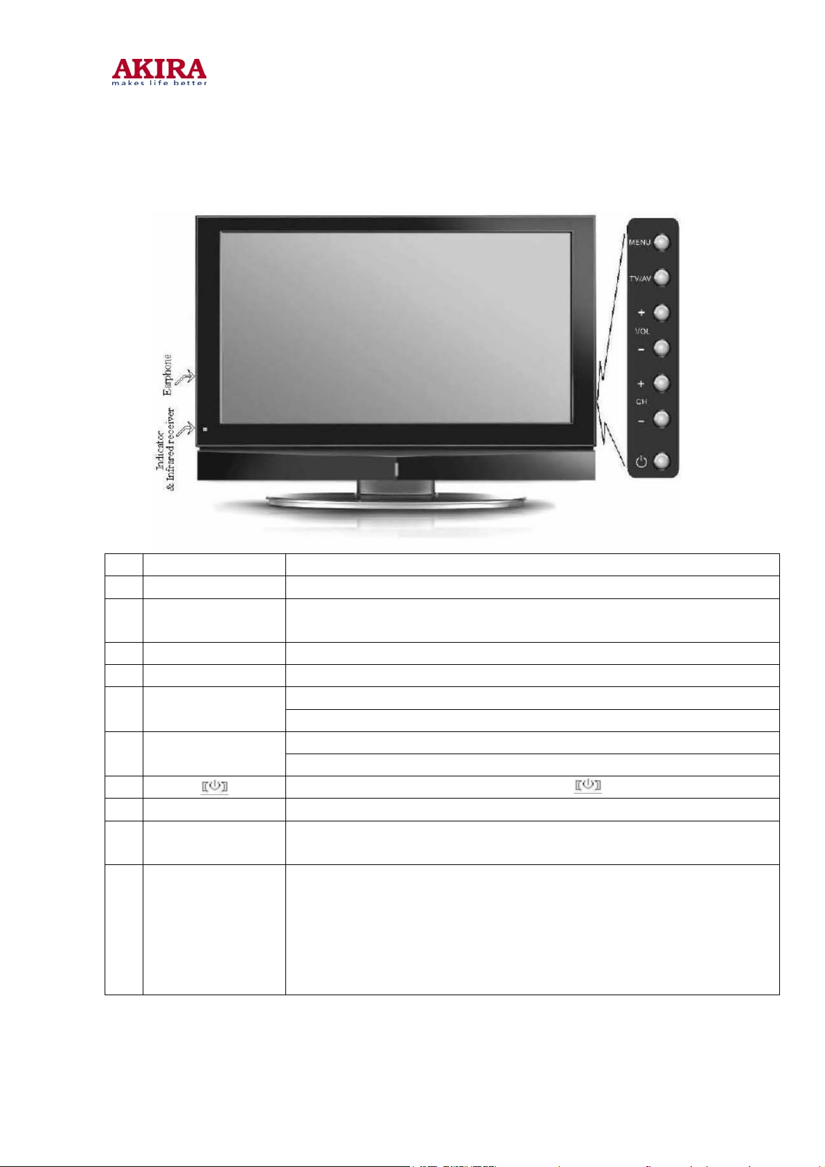
AAPPPPEEAARRAANNCCEE && FFUUNNCCTTIIOONN CCOONNTTRROOLL
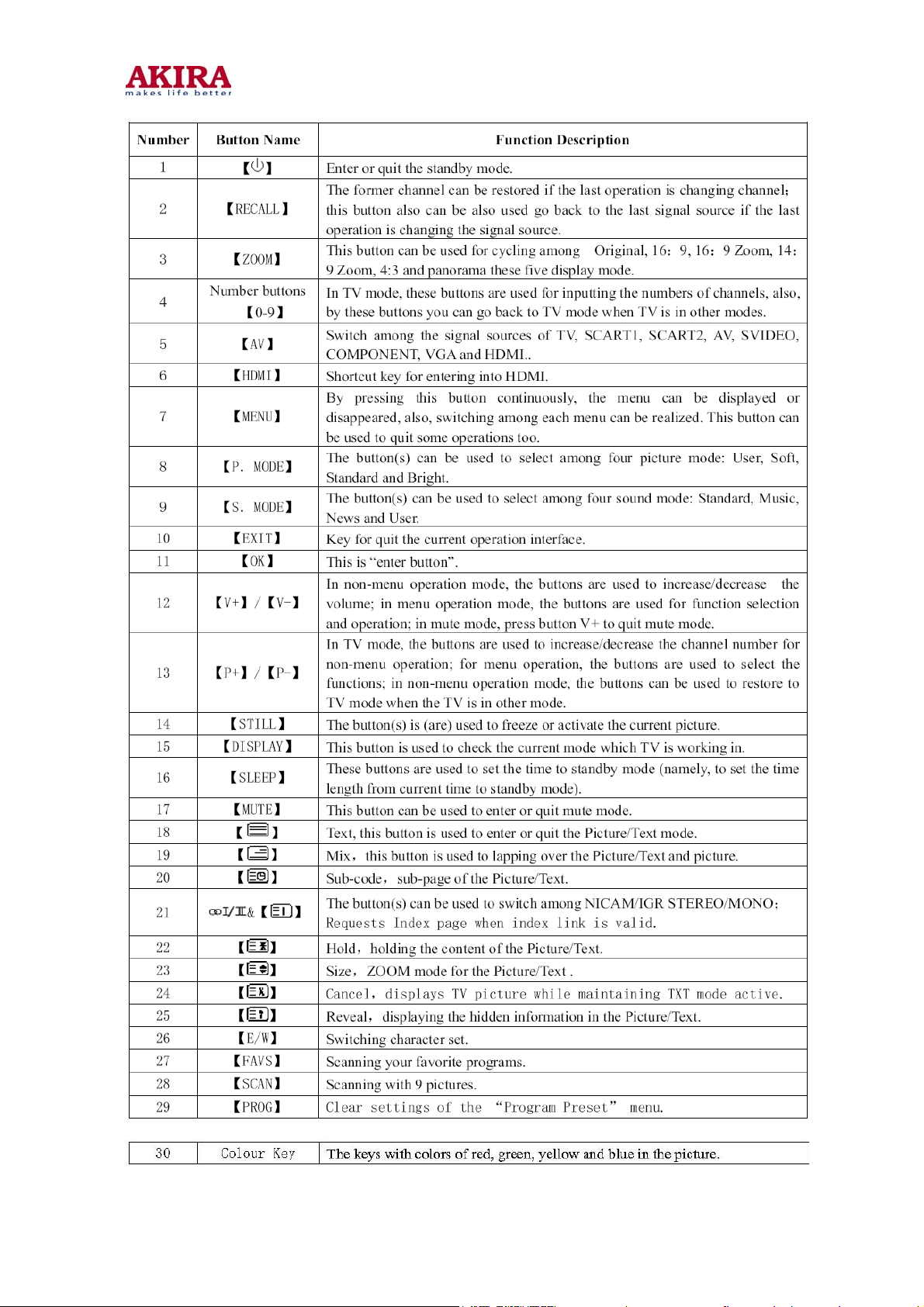
No. NAME DESCRIPTION
○1
○2
○3
○4
○5
○6
○7
(1) Headphone Output Port for headphone audio output
(2)
(3) Power Indicator
Notice: In this manual, the icon with “< >” means the button on the remote control, the icon with “[ ]” mean
the button on the LCD TV.
<MENU> Open the menu switch among the menus
<TV / AV>
<VOL+> To increase the sound volume , Adjust functions in menu operation.
<VOL-> To decrease the sound volume, Adjust functions in menu operation.
<CH+>
<CH->
Infrared Receiver
Window
To switch among the signal source of TV, SCART1, SCART2, AV,
S-VIDEO, COMPONENT, VGA and HDMI
1. In TV mode, increase channel number
2. To select functions in menu operation
1. In TV mode, decrease channel number
2. To select functions in menu operation
Enter or leave the standby mode, same as
To receive the signal from remote control
Red indicator lighting, this means the TV is in standby mode; Red indicator (lighting for
10 seconds) and yellow indicator (lighting for 5 seconds) by times, this means the TV is
in standby mode and the time to turning on the TV is set; Green indicator lighting this
means the TV is in normal working condition; Green indicator (lighting for 10 seconds)
and Red indicator (lighting for 5 seconds) by turns, this means the TV is in normal
mode with setting time to turning off or setting the sleeping TV off mode.
on the remote control.
Model No.:LCT-37CH01ST.doc
Version:1.0
7
Page 8
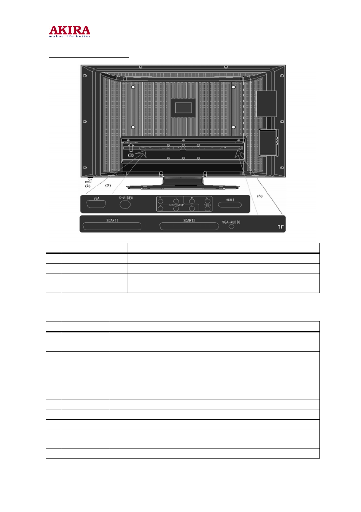
REAR SIDE OF LCD
No. Name Function
(1) Power Socket AC power input for LCD TV
(2) Switch of AC Power Turn on & Off the AC power of TV
(3) Signal Input / Output
terminal
Terminal Description:
No. Name Description
VGA Connect the VGA signal of computer with this port VGA cable, connect audio signal
○1
S-VIDEO Brightness and chroma signal input, Notice: S-Video and AV can not be used at
○2
COMPONENT
○3
AV AV audio / video signal input terminal
○4
HDMI Port for digital audio & video signal input
○5
SCART1 Video and RGB signal input, Video signal (RF VIDEO signal) output
○6
SCART2 Video and Y/C signal input, Video signal (RF VIDEO signal) output
○7
Headphone
○8
Output
TV Signal input TV signal input port
○9
with VGA’s audio input port by audio cable.
same time for they share of one signal channel.
Connect the TV COMPONENT signal port with video COMPONENT signal from
DVD or other equipments.
Port for headphone audio output
Including audio / video input of AV, S-Video, SCART1, SCART2, Component,
VGA and HDMI.
Model No.:LCT-37CH01ST.doc
Version:1.0
8
Page 9
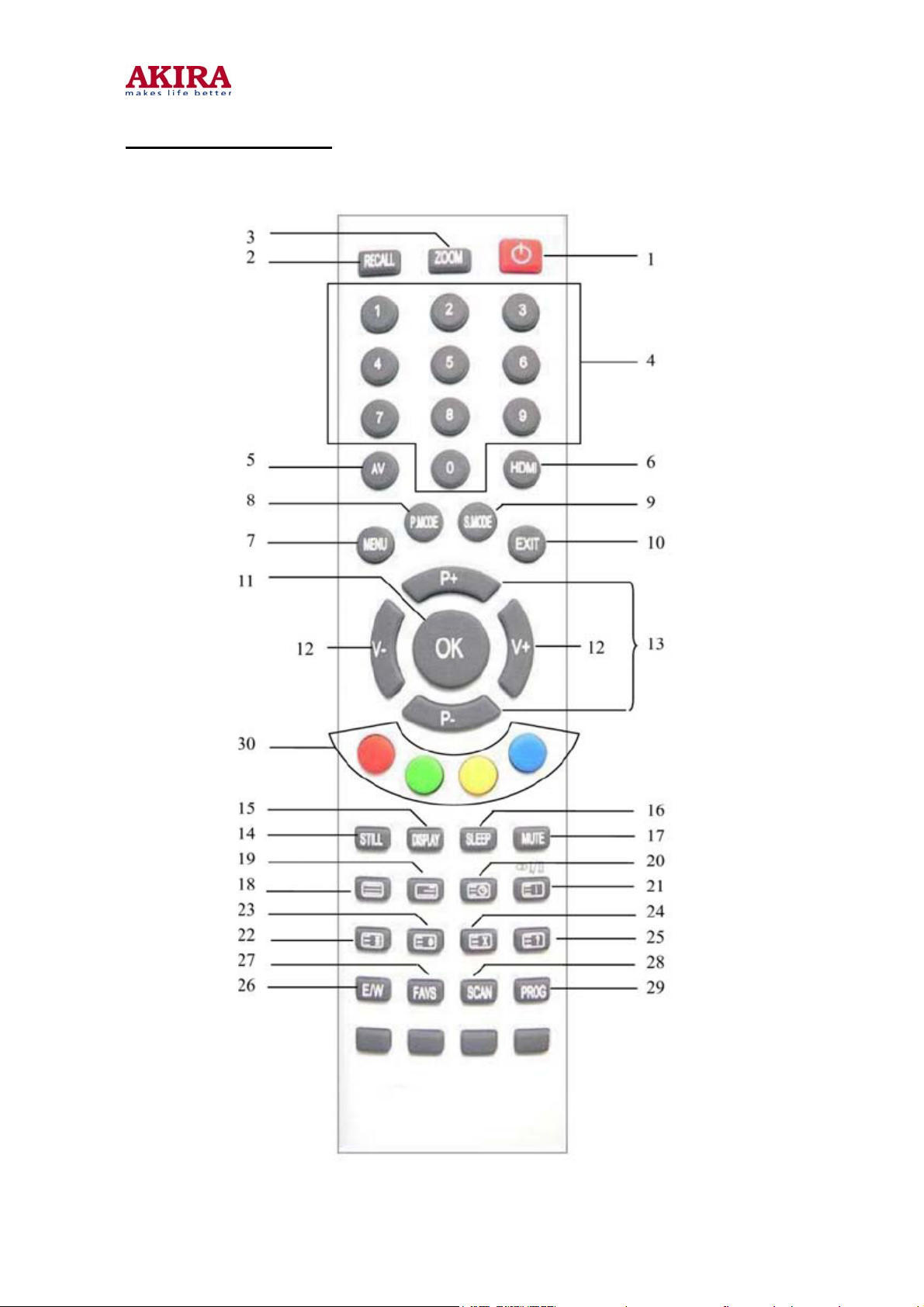
REMOTE CONTROL
The buttons of the original remote control are as following:
Model No.:LCT-37CH01ST.doc
Version:1.0
9
Page 10
Model No.:LCT-37CH01ST.doc
Version:1.0
10
Page 11
OOPPEERRAATTIIOONN
Model No.:LCT-37CH01ST.doc
Version:1.0
11
Page 12
Model No.:LCT-37CH01ST.doc
Version:1.0
12
Page 13

Model No.:LCT-37CH01ST.doc
Version:1.0
13
Page 14
Model No.:LCT-37CH01ST.doc
Version:1.0
14
Page 15
Model No.:LCT-37CH01ST.doc
Version:1.0
15
Page 16
Model No.:LCT-37CH01ST.doc
Version:1.0
16
Page 17
Model No.:LCT-37CH01ST.doc
Version:1.0
17
Page 18
Model No.:LCT-37CH01ST.doc
Version:1.0
18
Page 19

Model No.:LCT-37CH01ST.doc
Version:1.0
19
Page 20
Model No.:LCT-37CH01ST.doc
Version:1.0
20
Page 21
Model No.:LCT-37CH01ST.doc
Version:1.0
21
Page 22
Model No.:LCT-37CH01ST.doc
Version:1.0
22
Page 23
CChhaarraacctteerriissttiicc ooff CChhaassssiiss
1. Specifications
Region Europe America Other regions
Color
mode
RF signal
Video(or Y/C)signal
Program presetting 100 sets(0-99)
Sound Power (THD
≤7%)
Power voltage 100V~240V 100V~240V 100V~240V
Graphics and text 100 pages X 100 pages
VCHIP、CCD X Yes X
Sound NICAM、IGR BTSC NICAM、IGR
SCART interface Yes X X
VGA signal input Yes Yes Yes
YpbPr HD signal input Yes Yes Yes
HDMI digital signal
input
Ear pho n e Yes Yes Yes
OSD language
Automatic shut down if
no signal
Program reserve
function
Channel exchange
and sorting
Energy saving function
Plug and Play
Sound
mode
PAL 、SECAM NTSC、PAL M 、PAL N PAL 、NTSC、SECAM
PAL -D/K、B/G、I
SECAM- L/L’、 D/K、
B/G
PAL ,NTSC,
SECAM
5W+5W 5W+5W 5W+5W
Yes Ye s Yes
Multinational languages
(English, French,
German, Italian,
Portuguese etc)
Automatically enter into standby state after 5 minutes in TV no signal state
Capable of reserving 5 sets program jumping time, if time is up to the reserved time,
automatically jump to the corresponding program
Customer could rearrange the channels according to personal habit
Customer could adjust LCD screen backlight brightness manually. Appropriately
reducing the backlight brightness could save energy.
LCD TV could be used as computer screen, no need for the installation of software,
which is Plug and Play in real sense
NTSC-M/N、
PAL-M/N
PAL ,NTSC,
NTSC4.43,SECAM
68 sets(AIR:2-69)
125sets CABLE:1-125)
English, French,
Portuguese Spanish
PAL -D/K、B/G、I
SECAM-D/K、B/G
NTSC-M
PAL,NTSC,NTSC4.43,
SECAM
236 sets(0-235)
English, French, German,
Russian
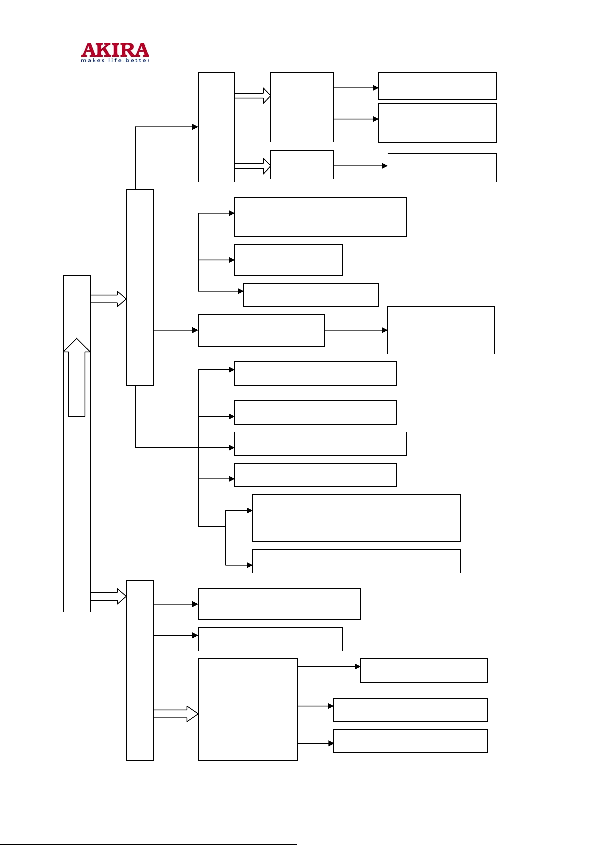
2. Circuit constitution
AKIRA LCD TV with LS01 chassis is made up of switch power, system control circuit, video
processing circuit, audio processing circuit, sound power amplifier circuit, AV input circuit,
LCD screen module. Block circuit diagram of the whole machine is shown as below:
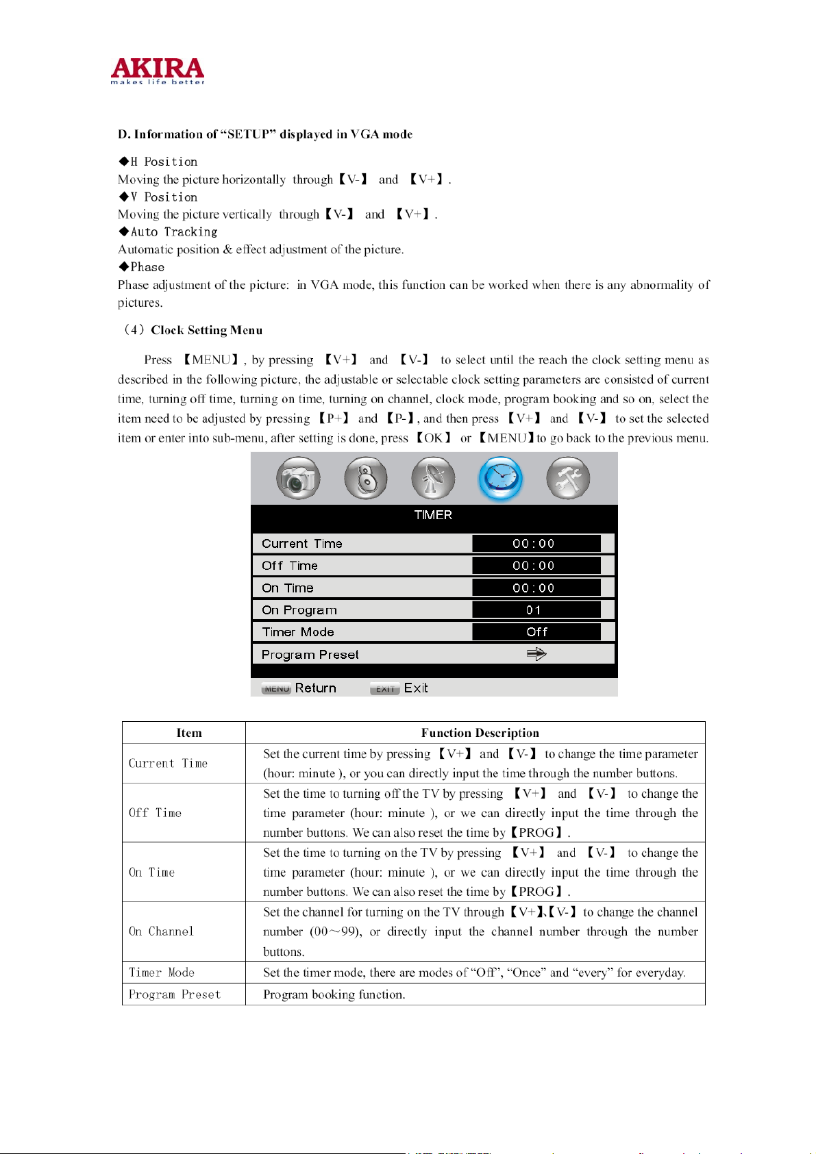
Model No.:LCT-37CH01ST.doc
Version:1.0
23
Page 24
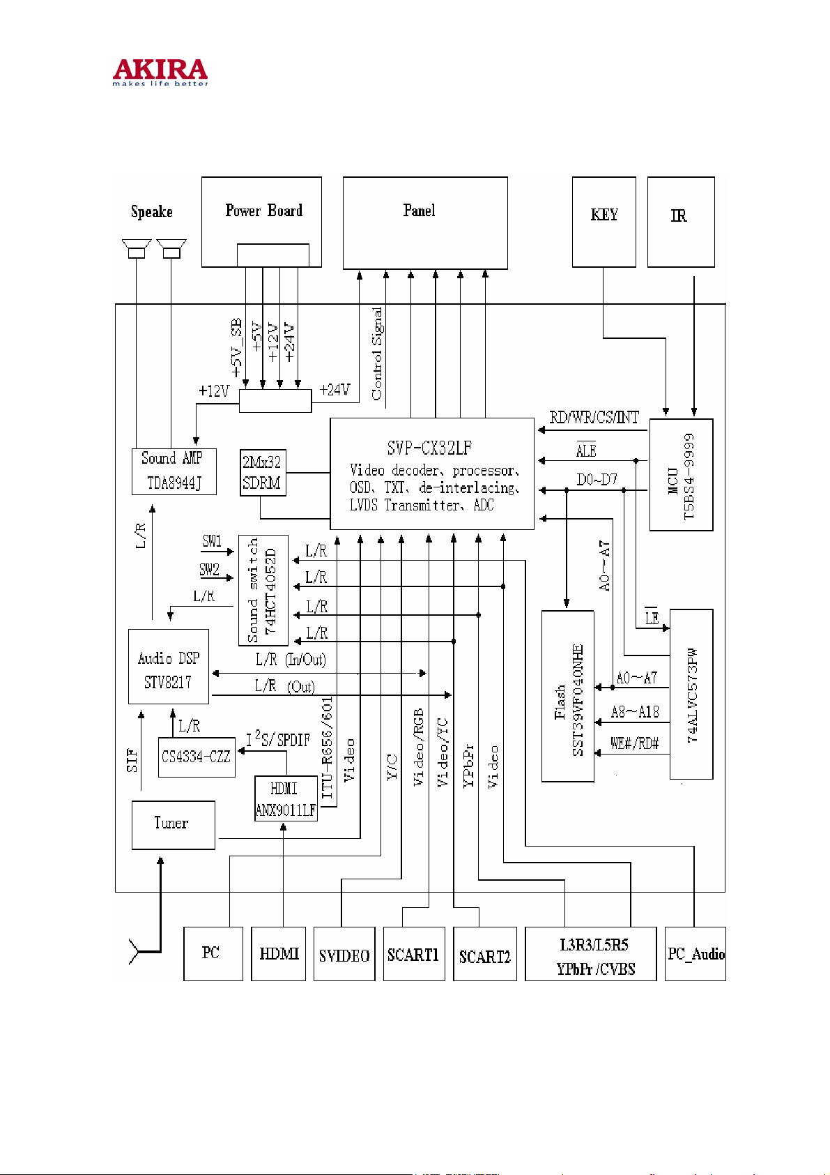
1) European market:
Model No.:LCT-37CH01ST.doc
Version:1.0
24
Page 25
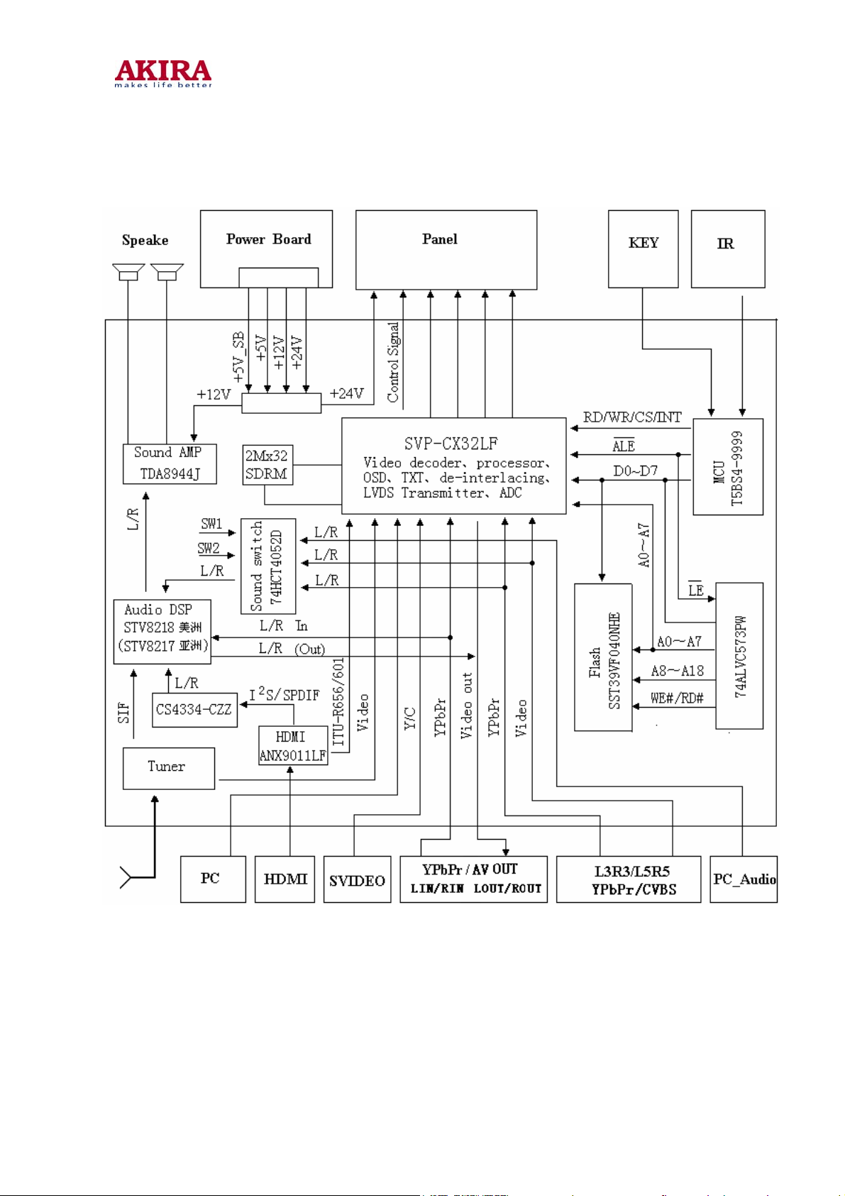
2). American and Asian market:
Model No.:LCT-37CH01ST.doc
Version:1.0
25
Page 26

j
3. Introduction of printed board module
AKIRA LCD TV with LS01 is made up of power board, side AV board, remote control reception board, key
board, and mainboard. The table below is the introduction of the function of all printed board modules.
No.
1
Module
Designation
Main
Board
Module
Main Board module is the chassis part of LCD TV signal processing. Under the control of
the system control circuit, It undertakes the task of converting the external input signal into
the unified digital signal that the LCD screen could identify. Mainboard controls the whole
machine through MCU bus, decode VIDEO signal, controls the image analog quantity
(brightness, contrast, chroma, hue, definition etc), adjusts white balance, generates OSD,
de-interlaces signal, converts signal frequency, and finishes signal A/D and D/A conversion,
video enhancement, LVDS signal coding and output; it has Scart interface, “S” terminal, AV
terminal, Ypbpr, HDMI and PC interface, Tuner input, sound demodulation, sound effect
treatment, sound power amplifier, and online upgrade of program.
Function Description
Remote
2
3
4
5
6 Side AV board Side AV board is used for earphone output.
Reception
Board
Module
Built-in
Power
Board
Module
Keyboard
Module
LCD screen
module
The remote reception board module is constituted by an indicator-light and a remote
reception-head. Customer could manipulate the LCD TV by using remote controller very
conveniently. By the color of the indicator light, the operation mode of the LCD TV could be
udged (red is standby, green is power on).
Convert the 100V~240V AC into DC, output have +24v, +12V, +5V, and the +5V_stb in
standby state.
Keyboard module has 7 function keys (program increase/decrease, volume
increase/decrease, AV/TV switch, menu key, on/standby control), customer could use the
key of the machine to manipulate the LCD TV.
LCD screen has built-in inverter that convert DC into high voltage AC signal to ignite the
backlight CCFL (Cold Cathode Fluorescent Light); the LCD screen process the video signal
from signal board and reappear.
Model No.:LCT-37CH01ST.doc
Version:1.0
26
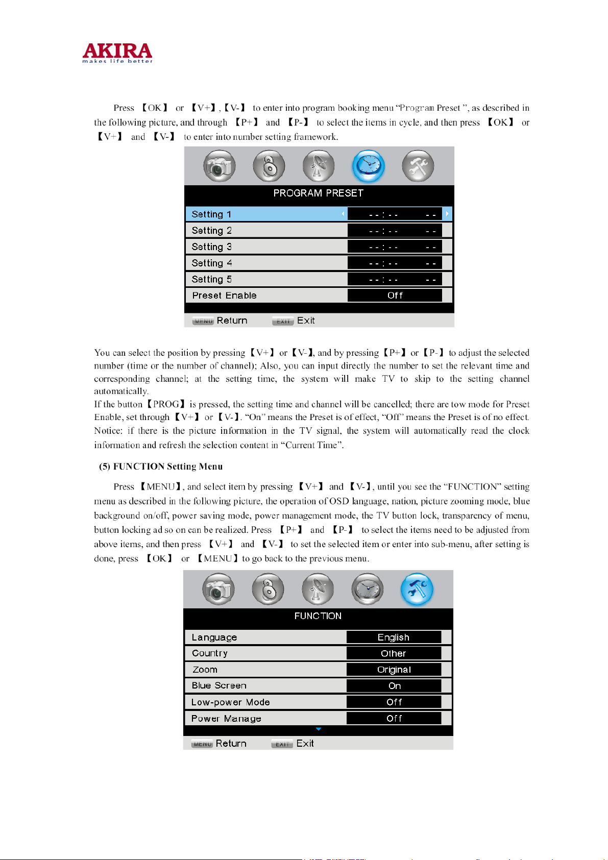
Page 27

FFuunnccttiioonn ooff mmaaiinn IICCss
1. Main ICs and functional modules
No. Item no. Model Main function
1 U15 JS-6H2/121 High frequency head, output sound and image video signal
2 U1 SVP-CX32LF Video decode, image processor, A/D and D/A conversion
3 U2 IS42S32200C1-6TL
4 U3 AT24C64A-10PU-2.7 EEPROM
5 U4 T5BS4-9999 MCU,main control IC
6 U5 SST39VF040-70-4C-NHE Flash, whole machine control program is in it
7 U6 74ALVC573PW Address latch, to latch the address wires
8 U8 TCM809SENB713 Hardware reset IC of MCU
9 U9 74HCT4052D Audio input switch of AV terminal
10 U35 STV-8217/STV-8218 Audio signal processor
11 U14 74LVC14AD VGA line and field synchronizing signal waveform shaping
12 U16、U25 AT24C02BN-10SU-1.8 EEPROM
14 U18、U22 AZ1117H -1.8TRE1 3.3V to 1.8V DC level conversion
16 U19、U24 AZ1117H -3.3TRE1 5V to 3.3V DC level conversion
18 U20 AZ1084S -3.3TRE1 5V to 3.3V DC level conversion
SDRAM with 2MX32bits, used for the access of image
signal.
19 U21 AZ1084S -1.8TRE1 5V to 1.8V DC level conversion
20 U23 AZ78L08ZTR-E1 12V to 8V DC level conversion
21 U26 CS4344-CZZ HDMI digital audio decode, D/A conversion
22 U28、U29 Rclamp0514M.TBT ESD protection device of HDMI input terminal
24 U30 ANX9011L HDMI digital signal decode
25 U31 PI5C3306LE Bus (SDA, SCL) switch used for program update
26 U33 TDA8944J Sound power amplifier (BTL output)
Model No.:LCT-37CH01ST.doc
Version:1.0
27
Page 28

2. Function introduction of ICs or functional module
1.Hign frequency head(JS-6H2/121)
Pin No. Definition of Pin Function Description
1 NC No connection
2 BT No connection
3 VCC +5V power
4 SCL IIC bus (clock)
5 SDA IIC bus (data)
6 AS Ground
7 AFS Ground
8 NC No connection
9 NC No connection
10 NC No connection
11 SIF/Out AGC control (intermediate audio output)
12 Video/Out CVBS signal output
13 VCC(+5V) +5V power
14 Audio/Out Audio signal output
2. Image processing IC SVP-CX32LF
SVP-CX32 is a high integrated video decoding, image processing chip and is widely used in such
mainstream flat screen TVs as HDTV, PC, LCD TV, and Plasma TV etc. it inherited the technological advantage
of its earlier stage scaler chip. It adopts the 6th generation Trident multi-zooming mode and non-interlaced
scanning technology when processing image. Multi-color mode (PAL/SECAM/NTSC) decoding is built-in; 10bit
A/D module, 8bit LVDS transmission interface, digital comb filter module, and 3D digital comb video decoding
are available. Such functions as video enhancement, OSD and VBI/Closed Caption, and teletext(LEVEL 2.5)
are available. The function of the chip makes it adapt to global market. The decoder could operate under
PAL/SECAM/NTSC mode; there are such input interfaces as 5 channels CVBS, 2 channels chroma signal, 1
channel PC RGB, 2 channels YpbPr, and 8-bit Digital ITU-R656/601(HDMI interface)。
Its main features are:
● 6th generation image dynamic smooth filtering
● 10-bits A/D conversion
● PC automatic phase and mode recognition, white balance correction
● 8bits LVDS transmission interface
th
generation 4 zooming watch mode
● 6
● Advanced chroma processing and dynamic contrast function
● Chroma extension of green and blue color, skin strengthen
th
generation 3D digital comb video filter
● 6
● Support 60Hz~100Hz interlace scanning and 50Hz~75Hz non-interlace scanning
● PC and video frame format conversion
● 14D dynamic video enhancement
● Pulse width modulation
● Build-in A/D conversion function
● Teletext function / Multi-image browse mode
● Provide 16/32bits SDR memory interface
Model No.:LCT-37CH01ST.doc
Version:1.0
28
Page 29

Pin function description:
Pin No. Designation of Pin Function of Pin
Analog signal input/output terminal
169 CVBS1 CVBS1 input
180 Y_G1 Y input terminal
181 Y_G2 SCART1 green base color input terminal
182 Y_G3 S terminal brightness signal input terminal
183 PC_G PC green base color input
188 PR_R1 DVD interface Pr signal input
189 PR_R2 SCART1 red base color input terminal
190 PR_R3 SCART2 brightness signal input terminal
191 PC_R PC red base color input
192 C S terminal brightness signal input terminal
196 PB_B1 DVD interface Pb signal input
197 PB_B2 SCART1 blue base color input terminal
198 PB_B3 SCART1 CVBS signal input terminal
199 PC_B PC blue signal input
171 FS1 No connection
170 FS2 No connection
173 FB1 SCART1 RGB_ST signal input terminal
172 FB2 SCART2 chroma signal input terminal
174 VREFP_1 A/D conversion1differential positive voltage
175 VREFN_1 A/D conversion 1 differential negative voltage
184 VREFP_2 A/D conversion 2 differential positive voltage
185 VREFN_1 A/D conversion 2 differential negative voltage
Digital signal terminal
37 DP0
┆ ┆
29 DP8
26 DP9
25 DP10
24 DP11
22 DP12
21 DP13
18 DP14
┆ ┆
14 DP18
11 DP19
┆ ┆
7 DP23
CPU control terminal
Digital signal I/O(DP0~DP23)interface
Model No.:LCT-37CH01ST.doc
Version:1.0
29
Page 30

55 PWMO Pulse width modulation input
57 SCL
58 SDA
60 GPIO0 GPIO1 selection signal
59 GPIO1 GPIO2 selection signal
62 WR# CPU write signal
63 RD# CPU read signal
61 CS
56 INTN
84 ALE Address latch signal
86 RESET Reset signal (high level effective)
85 V5SF
4 DP_HS Line synchronization signal
5 DP_VS Field synchronization signal
23 DP_CLK Clock signal
6 DP_DE_FLD DE I/O terminal
64 ADDR0
┆ ┆
71 ADDR7
83 A_D0
┆ ┆
76 A_D7
MISC port control signal
162 CVBS_OUT2 SCART2 interface CVBS signal output
163 CVBS_OUT1 SCART1 interface CVBS signal output
157 TEST MODE Test mode signal (grounding)
158 AIN_HS Line synchronization signal
159 AIN_VS Field synchronization signal
205 XTALI
204 XTALO
SDRM
124 MA0
┆ ┆
121 MA3
118 MA4
┆ ┆
113 MA9
125 MA10
126 MA11
156 DQM0
133 DQM1
109 DQM2
IIC bus(clock)
IIC bus(data)
CPU chip selection signal(low level effective)
Interrupt signal(low level effective)
SF Power(+5V)
CPU address(R0~R7)signal
CPU address/data passage
Crystal oscillator interface
Memory address (A0~A11)
Memory read/write byte signal
Model No.:LCT-37CH01ST.doc
Version:1.0
30
Page 31

87 DQM3
128 BA0
127 BA1
130 RAS# RAS signal
131 CAS# CAS signal
132 WE# Memory write drive
112 CLKE Memory clock signal drive
129 CS0# Memory chip selection signal
111 MCK Memory clock signal
155 MD0
┆ ┆
148 MD7
145 MD8
┆ ┆
138 MD15
107 MD16
┆ ┆
100 MD23
95 MD24
┆ ┆
88 MD31
LVDS port
52 LVDS_VDDP LVDS channel power
38 PLL_GND PLL ground
39 PLL_VCC PLL power
47 LVDSGND LVDS ground
46 LVDSVCC LVDS channel power
43 TCLK1M
41 TCLK1P
51 TA1 M
50 TA1P
49 TB1M
48 TB1P
45 TC1M
44 TC1P
41 TD1M
40 TD1P
Clock and power
146 VDDM
134 VDDM
108 VDDM
98 VDDM
Memory stack address selection
Memory data interface
High, low differential clock port
High, low differential data port
Memory port digital power
Model No.:LCT-37CH01ST.doc
Version:1.0
31
Page 32

72 VDDH
19 VDDH
160 VDDC
136 VDDC
119 VDDC
96 VDDC
74 VDDC
53 VDDC
27 VDDC
12 VDDC
13 VSSC
28 VSSC
54 VSSC
75 VSSC
97 VSSC
120 VSSC
137 VSSC
161 VSSC
20 VSSH
73 VSSH
99 VSSM
110 VSSM
135 VSSM
147 VSSM
195 AVDD3_ADC2
168 AVDD3_ADC1
2 PLF2 Video PLL clock low pass filtering
207 MLF1 Memory PLL clock low pass filtering
1 PAVSS2 PLL ground
3 PAVDD2 PLL power (+1.8V)
206 PAVSS1 PLL digital ground
208 PAVDD1 PLL digital ground power (+1.8V)
203 PAVSS PLL Digital ground
202 PAVDD PLL digital ground power(+1.8V)
201 PDVSS PLL Digital ground
200 PDVDD PLL digital ground power (+1.8V)
177 AVDD_ADC1
186 AVDD_ADC2
193 AVDD_ADC3
178 AVDD_ADC4
176 AVSS_ADC1
187 AVSS_ADC2
3.3V power supply
1.8V power supply
Digital ground
ADC module power (+3.3V)
ADC analog power (+1.8V)
ADC analog ground
Model No.:LCT-37CH01ST.doc
Version:1.0
32
Page 33
194 AVSS_ADC3
179 AVSS_ADC4
165 AVDD3_OUTBUF
164 AVSS_OUTBUF
166 AVDD3_BG_ASS
167 AVSS_BG_ASS
+3.3V analog power
Analog ground
Model No.:LCT-37CH01ST.doc
Version:1.0
33
Page 34

SVP-CX32LF internal block diagram:
Model No.:LCT-37CH01ST.doc
Version:1.0
34
Page 35

3.T5BS4-9999 brief introduction:
T5BS4-9999 is a 16-bit high-speed micro-controller that is used for the control of a variety of
small to large devices. T5BS4-9999 could extend ROM and is an IC with 64 pins and is
packaged in PLCCC. It is the main control IC of the TV and implements I²C bus control of the
overall system.
Main features:
(900/L1 CPU)16bit high speed CPU(900/L1 CPU)
● Minimum time of 148ns in accomplishing instruction fetch
● Build-in 10K RAM
● 16M external extended memory
● simultaneously support 8-/16-bit external data bus
● 8-bit cycle for channel, 16-bit cycle for 1-control
● 1-channel universal serial interface
● 1-channel IIC bus mode serial interface
● 4-way 10 bit A/D conversion interface
● Clock monitor
● Real time control clock
● 4 chips selection/wait controller
● 34 interrupt signals output
9 CPU interrupt, 21 internal interrupt, 4 external interrupt
● 53 I/O pins
● Reserved wait function
● Clock control
fs=32.768KHz real-time time of time conversion function high frequency fc to fc/16
● Working voltage
When fc=27 MHZ, VCC=2.7~3.6V, when fc=10MHZ, VCC=1.8V to 3.6V
● 64 pin package(P-LQFP64-1010-0.50D standard)
Model No.:LCT-37CH01ST.doc
Version:1.0
35
Page 36
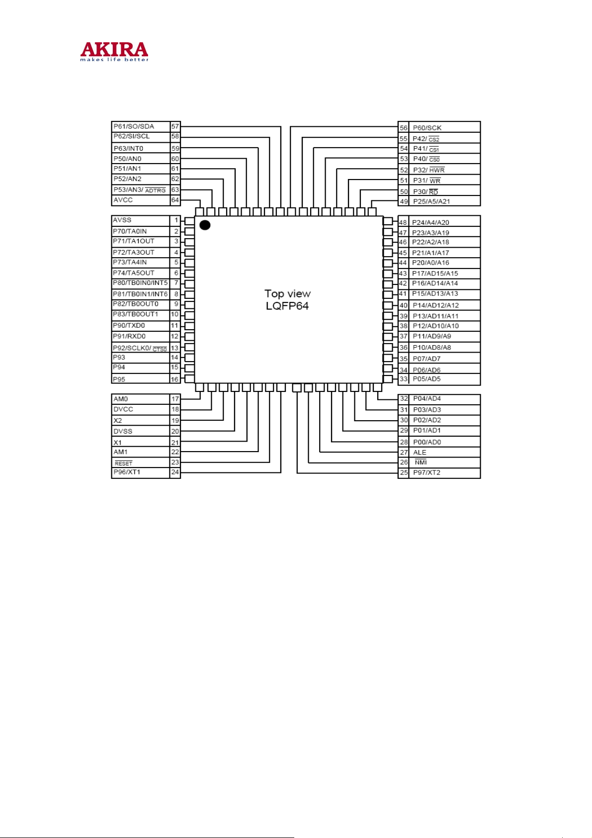
Pin allocation description:
Model No.:LCT-37CH01ST.doc
Version:1.0
36
Page 37
Pin introduction:
Pin Designation Function description
1
2
3 P71/TA1OUT I²C bus clock output
4 P72/TA3OUT PAGE signal output
5 P73/TA4IN +5V power
6 P74/TA5OUT Backlight on/off control
7 P80/TB0IN0/INT5 Remote control signal
8 P81/TB0IN1/INT6 +1.8V power supply
9 P82/TB0OUT0 Remote red control signal
10 P83/TB0OUT1 Remote green control signal
11 P90/TXD0 Digital ground
12 P91/RXD0 HDMI identity signal
13 P92/SCLK0/ No connection
14 P93 CON4(10th pin)
15 P94 CON4(4th pin)
16 P95 CON4(3rd pin)
17 AM0 Bus byte selection
18 DVCC +3.3V power
19 X2 Crystal oscillator interface
20 DVSS Ground
21 X1 Crystal oscillator interface
22 AM1 Bus byte selection
23 CPU reset control port
24 P96/XT1 Low frequency oscillation input interface
25 P97/XT2 Low frequency oscillation output interface
26 NMI Interrupt request signal
27 ALE Address latch level
28 P00/AD0
┆ ┆
35 P07/AD7
36
┆
43
AVSS Analog ground
P70/TA0IN I²C bus data input
0~7 bit address/data channel
P10/AD8/A8
┆
P17/AD15/A15
8~15 bit address/data channel
or 8~15 bit address channel
44
┆
49
50 P30/ External memory read control terminal
51
52 P32/ Data write control terminal (AD8~AD15)
Model No.:LCT-37CH01ST.doc
Version:1.0
P20/A0/A16
┆
P25/A5/A21
P31/
8~5 bit address channel
or 8~21 bit address channel
External memory write control terminal (AD0~AD7)
37
Page 38
53 P40/
54 P41/
55 P42/
56 P60/SCK (no connection)
57 P61/SO/SDA I²C bus data
58 P62/SI/SCL I²C bus clock
59 P63/INT0 Interrupt request signal
60 P50/AN0
61 P51/AN1
62 P52/AN2 SCART1 interface FS signal
63 P53/AN3/ SCART2 interface FS signal
64 AVCC Analog power (+3.3V)
Model No.:LCT-37CH01ST.doc
Version:1.0
Internal address selection signal
KEY control terminal
38
Page 39

T5BS4-9999 internal functional block diagram:
Model No.:LCT-37CH01ST.doc
Version:1.0
39
Page 40
4.STV-8217/STV-8218 brief introduction
STV-8217/STV-8218 is capable of following functions:
■ Full-Automatic Multi-Standard Demodulation
● B / G / I / L / M / N / D / K Standards
● Mono AM and FM
● FM 2-Carrier and NICAM/BTSC
■ Sound Processing: Loudspeaker
● ST royalty-free processing: ST WideSurround, ST
OmniSurround (Virtual Dolby
Virtual Dolby
Bass
● Independent Volume / Balance
● Smart Volume Control (SVC), 5-band equalizer and
Loudness
■ Analog Audio Matrix
● 4 stereo inputs
● 3 stereo outputs
● THRU mode
● 2 VRMS capability
Pin introduction:
ٛ Digital compliant) and ST Dynamic
ٛ Surround and
Pin Designation Function Description
1 SC1_OUT_L SCART1 left audio output
2 SC1_OUT_R SCART1 right audio output
3 VCC_H +8V power
4 GND_H ground
5 SC3_OUT_L SCART3 left audio output
6 SC3_OUT_R SCART3 right audio output
Model No.:LCT-37CH01ST.doc
Version:1.0
40
Page 41

Pin Designation Function Description
7 VCC33_SC +3.3V power
8 GND33_SC Ground
9 SC1_IN_L SCART1 left audio output
10 SC1_IN_R SCART1 right audio output
11 VREFA Sound bypass voltage decoupling interface
12 GND_SA Ground
13 VBG Sound sideband voltage decoupling interface
14 SC2_IN_L SCART2 left audio input
15 SC2_IN_R SCART2 right audio input
16 VCC33_LS DACs power(+3.3V)
17 GND33_LS DACs ground
18 SC2_OUT_L SCART2 left audio output
19 SC2_OUT_R SCART2 right audio output
20
VCC_NISO
GND_SA
21 VSS33_CONV DAC ground
22 VDD33_CONV DAC power (+3.3V)
23 SC3_IN_L SCART3 left audio input
24 SC3_IN_R SCART3 right audio input
25 SCL_FLT SCART left channel filtering
26 SCR_FLT SCART right channel filtering
27 LS_C No connection
28 LS_L Loudspeaker left channel output
29 LS_R Loudspeaker right channel output
30 LS_SUB No connection
31 HP_LSS_L No connection
32 HP_LSS_R No connection
33 VSS18_CONV DAC/ADC ground
NISO polarization voltage(+3.3V)
DACS ground
34 VDD18_CONV DAC/ADC power (8V)
35 /HP_DET Earphone connection test terminal
36 ADR_SEL Chip address selection signal
37 VSS18 Digital ground
38 VDD18 +1.8V power
39 SCL I²C bus clock
Model No.:LCT-37CH01ST.doc
Version:1.0
41
Page 42

Pin Designation Function Description
40 SDA I²C bus
41 VSS18 Digital ground
42 VDD18 +1.8V power
43 /RST Reset signal input/output terminal
44 S/PDIF_IN No connection
45 S/PDIF_OUT No connection
46 VDD33_IO1 +3.3V power
47 VSS33_IO1 Digital ground
48 CK_TST_CTRL Digital ground
49 VSS18 Digital ground
50 VDD18 +1.8V Power
51 CLK_SEL Clock input format selection
52 XTALIN_CLKXTP
53 XTALOUT_CLKXTM
54 VCC18_CLK1 5V regulated output
55 GND18_CLK1 Ground
56 GND18_CLK2 Ground
57 VCC18_CLK2 +1.8V Power
58 VSS33_IO2 Digital ground
59 VDD33_IO2 +3.3V Power
60 I2S_PCM_CLK No connection
61 I2S_SCLK I²S clock I/O channel1,2,3
62 I2S_LR_CLK I²S selection signal input/output
63 I2S_DATA0 I²S bus data input/output stereo channel 1
64 I2S_DATA1 I²S bus data input stereo channel 2
65 I2S_DATA2 I²S bus data input stereo channel 3
66 VDD18 +1.8V Power
Oscillator interface
67 VSS18 Ground
68 BUS_EXP Bus extension selection
69 IRQ No connection
70 GND_PSUB Ground
71 VDD18_ADC +1.8V Power
72 VSS18_ADC Ground
73 SIF_P Intermediate audio input (positive terminal)
Model No.:LCT-37CH01ST.doc
Version:1.0
42
Page 43

Pin Designation Function Description
74 SIF_N Intermediate audio input (negative terminal)
75 GNDPW_IF Ground
76 VCC18_IF +1.8V Power
77 GND18_IF Ground
78 MONO_IN High frequency head audio input
79 SC4_IN_L SCART4 left audio input
80 SC4_IN_R SCART4 right audio input
Model No.:LCT-37CH01ST.doc
Version:1.0
43
Page 44

STV-8217 internal block diagram:
Model No.:LCT-37CH01ST.doc
Version:1.0
44
Page 45

STV-8218 internal block diagram:
Model No.:LCT-37CH01ST.doc
Version:1.0
45
Page 46

5.TDA8944J brief introduction:
TDA8944J is a dual channel sound power amplifier, with each channel has 7W power output (the resistance
of the loudspeaker is 8Ω) to drive the loudspeaker; When music is played, its high efficiency could reduce
external heat dispersion and the requirement of the power supply equipment.
Its main features:
● High integration
● Standby and mute mode
● No switch switching noise
● 12V Power filtering
● Low working current
● Output current short-circuit grounding protection
● Overheat protection
● Linear output to drive external earphone, PC and portable audio equipment
Pin introduction:
Pin Designation Function Description
1 OUT1 Loudspeaker negative pole output terminal 1
2 GND1 Ground
3 VCC1 +12V Power
4 OUT1 Loudspeaker positive output terminal 1
5 N.C. No connection
6 IN1 Positive pole input terminal 1
7 N.C. No connection
8 IN1 Negative pole input 1
9 IN2 Negative pole input 2
10 MODE Operation mode selection (standby, mute, work)
11 SVR Voltage decoupling filtering (grounding)
12 IN2 Positive pole input terminal 2
13 N.C. No connection
14 OUT2 Loudspeaker negative output terminal 2
15 GND2 Ground
16 VCC2 +12V Power
17 OUT2+ Loudspeaker positive output terminal 2
Model No.:LCT-37CH01ST.doc
Version:1.0
46
Page 47

TDA8944J internal block diagram:
6. ANX9011L brief introduction:
ANX9011L is a processor used for HDMI (high definition multimedia interface) signal reception processing,
and is used in digital TV, platform screen TV, and projection equipment. It receives the HDMI input data series
and decodes them into digital audio and digital video signal. ANX9011L could input and output 8 channels digital
audio channel of 192kHz sampling frequency, it has 128 pins with LQFP packaging and has a build-in HDCP,
which could greatly reduce design complexity and system cost.
Its main features are:
● Support up to 165MHz HDMI data rate
● Suitable for HDMI 1.1,HDCP 1.1 and DVI 1.0 format
● Support 20m connection cable
● Support multi-format video processing
24 bit RGB / YCbCr 4:4:4
16/20/24 bit YCbCr 4:2:2
8/10/12 bit YCbCr 4:2:2 (ITU BT656)
12bit two data rate interface
24/48 bit single data rate interface
● RGB and YcbCr color format conversion of each other
● Auto configure video mode
● Digital audio interface
32-192kHz audio sampling rate
Provide 4-channel IIS interface for 8 audio channels
Mute software configuration
● HDCP decryption technology
● PRBS31 link auto-test technology
● Controllable Power protection management system
● 128 pin LQFP packaging
Model No.:LCT-37CH01ST.doc
Version:1.0
47
Page 48

Pin function
Pin Designation Function Description
Digital image output terminal
92 VDE23
┆ ┆
96 VDE19
99 VDE18
┆ ┆
101 VDE16
┆ ┆
105 VDE12
108 VDE11
┆ ┆
117 VDE4
121 VDE3
┆ ┆
124 VDE0
24bit(DP0~DP23)digital video output data bus
2 VDO23
┆ ┆
5 VDO20
8 VDO19
┆ ┆
11 VDO16
14 VDO15
┆ ┆
17 VDO12
20 VDO11
┆ ┆
23 VDO8
26 VDO7
┆ ┆
29 VDO4
32 VDO3
┆ ┆
35 VDO0
119 VD_CLK Video output data clock
127 DE Video output data effective level signal
128 HSYNC Line synchronizing signal
1 VSYNC Field synchronizing signal
Digital audio output terminal
24bit(QO0~QO23)no connection
85 XTAL_IN
Crystal oscillator interface
84 XTAL_OUT
Model No.:LCT-37CH01ST.doc
Version:1.0
48
Page 49
79 MCLKOUT Audio main control clock output
76 IIS_SCK IIS bus clock
75 IIS_WS IIS signal selection
74 IIS_SD0 IIS bus data
┆ ┆
71 IIS_SD3
70 SPDIF (no connection )
67 MUTEOUT Mute control signal (no connection )
Control signal port
91 INT Interrupt request output
89 RESETN Reset signal input
42 DDC_SCL DDC Clock signal
41 DDC_SDA DDC address/data signal
40 CFG_SCL I²C bus clock
39 CFG_SDA I²C address/data
90 HDMI_DET Synchronization detection
38 DEVAD I²C connection detection signal
44 HDMI_5V Cable insert detection terminal
88 RESDL Ground
43 NC
45 NC
HDMI signal input terminal
51 HDMI_CLKP
50 HDMI_CLKN
55 HDMI_D0P
54 HDMI_D0N
59 HDMI_D1P
58 HDMI_D1N
63 HDMI_D2P
62 HDMI_D2N
IIS channel selection (no connection)
No connection
Differential clock input
Differential data input1
Differential data input 2
Differential data input 3
Power and ground
DVDD18
DVDD33
AVDD33
DVSS
AVSS 46, 52, 56, 60, 64, 83 Analog ground
12, 24, 36, 51, 66, 81,
82, 112, 125
7, 19, 31, 68, 77, 98,
107, 120
47, 49, 53, 57, 61, 86,
87
6, 13, 18, 25, 30, 37,
65, 69, 78, 80, 97, 106,
113, 118, 126
+1.8V digital Power
+3.3V digital Power
+3.3V analog Power
Digital ground
Model No.:LCT-37CH01ST.doc
Version:1.0
49
Page 50

ANX9011L internal block diagram:
7. 74HCT4052D brief introduction:
74HCT4052D is a 4-channel bi-directional analog multiplexer and multi-channel output selector. Each
multi-channel output selector has 4 independent input/output terminals and 1 common input/output terminal. It
is often used in analog and digital multiplexing, and multi-channel output selecting circuit and signal control
system.
Its main features are:
● -5V to +5V widely range Power input
● Low on-resistance
● Logical level alternating
● Build-in interrupt before running
● In line with JEDEC no.7A standard
● Automatic protection function
Model No.:LCT-37CH01ST.doc
Version:1.0
50
Page 51
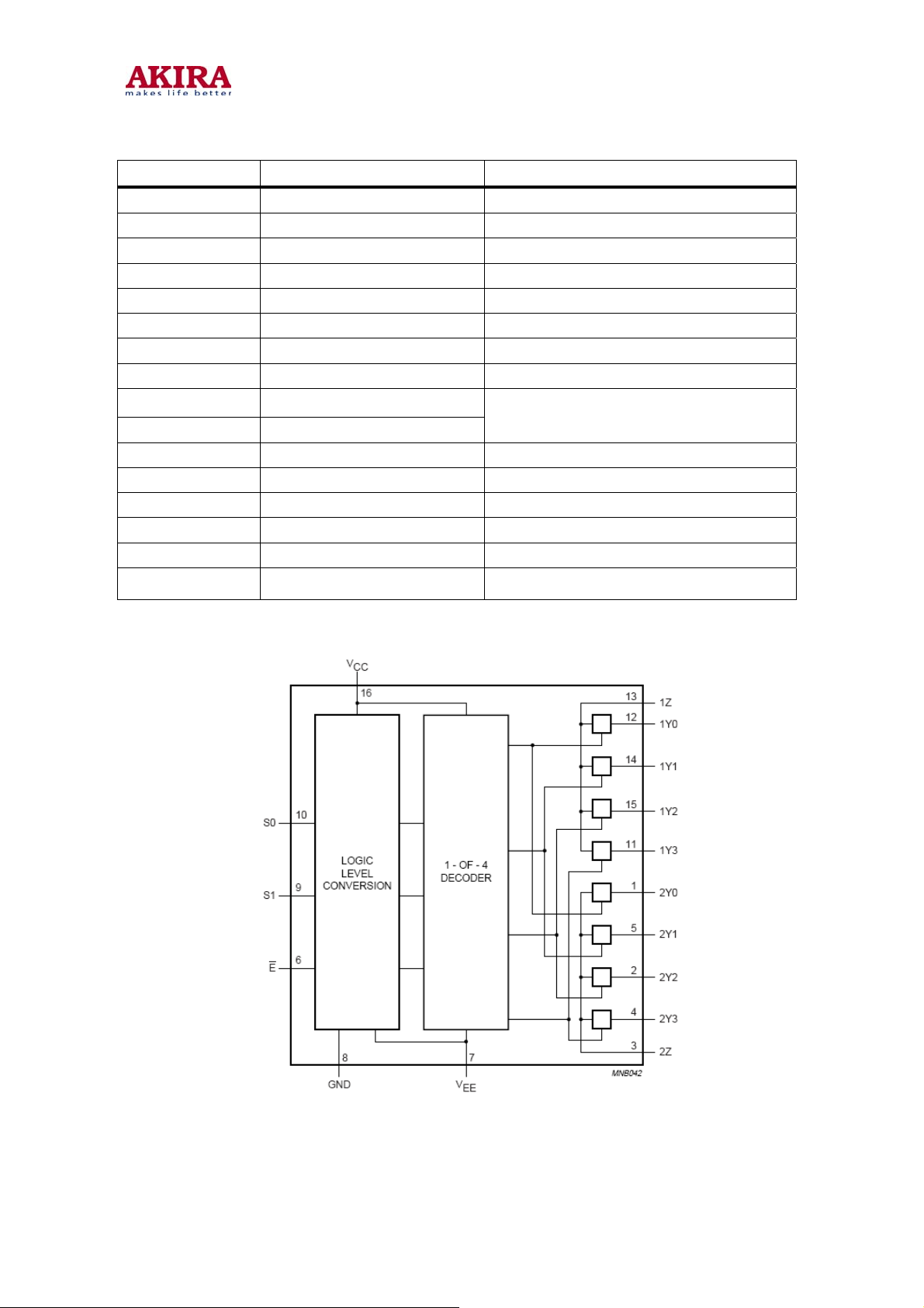
Pin introduction:
Pin Designation Function Description
1 2Y0 PC left audio input
2 2Y2 HD terminal left audio input
3 2Z Left audio input
4 2Y3 SCART2 left audio input
5 2Y1 AV left audio input
6 E Ground
7 VEE Ground
8 GND Ground
9 S1
10 S0
11 1Y3 SCART2 right audio input
12 1Y0 PC right audio input
13 1Z Right audio output
14 1Y1 AV right audio input
15 1Y2 HD terminal right audio input
16 VCC +5V Power
Select level input (+3.3V Power)
74HCT4052D internal block diagram:
Model No.:LCT-37CH01ST.doc
Version:1.0
51
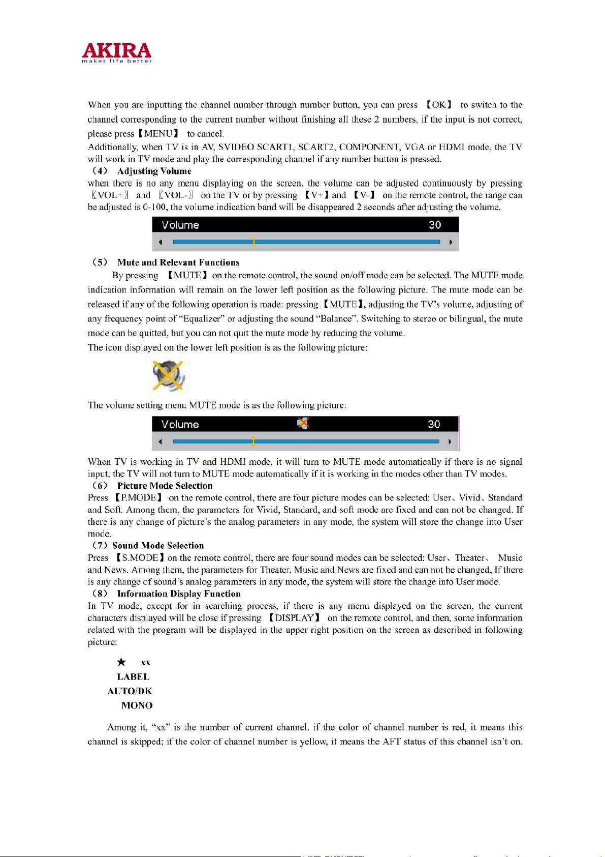
Page 52
,
SSiiggnnaall PPrroocceessssiinngg AAnnaallyyssiiss aanndd MMeeaassuurreedd DDaattaa
This chapter Mainly introduces the receiving and processing of image signal and sound signal, whole
machine system control process, and whole machine power supply system (Model of LT32GJ01E is taken as
an example, other models is similar and will not be explained here for each. There are minor differences in
power supply among different models of liquid crystal screen; the details are shown in Specifications).
1. Image signal flow
RF signal is demodulated by tuner, then the obtained video signal and signals inputted from COMPONENT
terminal, AV terminal, S terminal, 2-way Scart interface and VGA interface are all sent into video-processing IC
SVP-CX32LF to be processed. Input signals with different format are changed into uniform LVDS differential
signals, and are sent to liquid crystal screen. In addition, TV video signal is processed by SVP-CX32LF to
generate 2-way CVBS signal, which is used in 2-way Scart video output.
Signal inputted from HDMI interface is decoded into digital video signal, which is sent into video decoding IC
SVP-CX32LF to be processed. After procession, the obtained uniform LVDS differential signal is sent to liquid
crystal screen through LVDS interface to screen.
2.Sound flow
RF signal is demodulated by tuner, and then the obtained SIF signal (SIF-2 signal) and audio signal inputted
from Scart1 interface are directly processed by STV-8217. The output audio signal of STV-8217 is sent into
power amplifier TDA8944J, and the amplified signal is finally sent to speaker or earphone output.
Signals from HDTV terminal, AV terminal, Scart2 interface and PC Audio are first sent into 74HCT4052D for
choosing passages, and then sent into STV-8217 for demodulation and sound effect processing. The output
audio signal of STV-8217 is sent into power amplifier TDA8944J, and finally the amplified signals are sent to
speaker or earphone output.
After the demodulation and sound effect processing of STV-8217, there is an audio output which is used for
sound output of Scart1 terminal.
3. Whole machine power supply system
There are 4 ways of voltage output in the power panel: +24V(6A)、+12V(2A)、+5V(2A)and +5VS(1A).
+24V output is used by LCD screen; +12V output is used by power amplifier TDA8944J, and is also changed
into +8V output by AZ78L08ZTR-E1 to satisfy the need of STV-8217 IC; +5V output is changed into 1.8V output
and 3.3V output by DO (such as AZ1117H-1.8TRE1 and AZ1117H-3.3TRE1) to satisfy the needs ICs. +24V,
+12V and +5V outputs will be cut off in standby state. While +5VS output is the power supply of MCU, infrared
receiver and EEPROM etc, and will be cut off when the AC is turn off.
5V output will be divided into two ways: one way is changed into +3.3V and +1.8V analogue power supplies
through DC/DC converter for STV-8217 IC, ANX9011LF IC etc and peripheral circuits; other way is changed
into +3.3V and +1.8V digital power supplies through DC/DC converter for SVP-CX32 IC etc and peripheral
circuits, and this way of 5V voltage will be cut off in standby state, while the other way of 5V voltage supply
power especially for MCU, infrared receiver and EEPROM etc, and will not be cut off in standby state.
(1) Constitution and distribution of whole machine power supply
+12V power
supply
FB34
CON11
Pin 1,2,3
FB8
+12V power
FB34
supply
CON403
Pin 3
12V power amplifier TDA8944J
4
U23
AZ78L08ZTR-E1
12V
+12V(voltage of line to screen) CON1
Pin 1,2,3,4 (used by 37 inches screen)
Pin 3,16
12V shutdown mute circuit
8V
ST82X7
Pin 3
Model No.:LCT-37CH01ST.doc
Version:1.0
52
Page 53
(
,
,
,
,
)
,
,
,
20
2
A
108
S
3
3
1
3
3
,16,20,
R206
2.2mA
FB27
R3,R4
R213 FB1,FB2
FB26 FB29
FB23 FB30,32
R214
575m
FB
FB5,6
5V
FB22 FB4
11
10
9
L1,2
8
FB3
CON11 Pin 7
R2
+5V
FB21
L24
L21
L28,29,22
Model No.:LCT-37CH01ST.doc
Version:1.0
V
.
+
TRE
.
4
U20 AZ
U19 AZ1117H-3.3TRE1 +3.3V
U18
AZ1117H-1.8TRE1
Pin 7, 19, 31, 68, 77, 98, 107, 120
Pin 47, 86, 87
U30 Sil9011
Pin 49, 53, 57, 61
U30 Sil9011 pin 87,86
AZ1084S-1.8TRE1
AZ1117H-1.8TRE1
U21
U1 SVP-CX32 Pin 19,72
U1 SVP-CX32 Pin 165,166
U1 SVP-CX32 Pin 46, 39, 52
U1 SVP-CX32 Pin 155,156
Pin 1,15,29,43,3,9,35,41,49,55,75,81
U1 SVP-CX32 Pin 98, 108, 134,146
U35 ST8217
Pin 7
U35 ST8217 Pin 46
U22
+1.8V
CX_VA18
1.8V
CX_VL18
1.8V
U30 Sil9011
U2 IS42S32200C1-6TL
22
U35 ST8217 Pin51
U35 ST8217 Pin 42,76,54
Y4 27MHz XO voltage
U1 SVP-CX32
Pin 177
Pin 12, 24, 36, 51, 66,
81
178,186,193
U30 Sil9011
82, 112, 125
U1 SVP-CX32
Pin 200
Pin 12,27,53,74,96,
119,136,160
202,208,3
U1 SVP-CX32
53
Page 54
(
,
,
,
,
)
FB12
FB16
FB24
11
FB17
10
9
FB7
8
FB20
R232
R198
CON11 Pin7
R202
+5V
FB28
FB19 R207
R208
5V_SB(CON12 Pin1,2)
FB9
FB25
FB10
FB11
CON14 Pin 1
CON17 Pin 1
CON5 Pin 1
(3) Pin level schedule for Voltage regulators on mainboard
Model No.:LCT-37CH01ST.doc
Version:1.0
Starting up mute circuit
+5V(voltage of line to screen)CON1 Pin 1,2,3,4 (used by
screen less than 32 inches)
U30 Sil9011 Pin 44
Back light switch control
Back light height control
U26 CS4344-CZZ Pin 9
74LVC14AD AT24C02BN PI5C3306LE 0514M.TBT
U1(SVP-CX32)Pin 85,D7,8(BAV99L)Pin 2
J3 VGA terminal interface voltage
IIC Bus data interface
IIC Bus clock interface
AZ1117H-3.3TRE1
U9 74HCT4052D Pin 16
U15 JS-6B2/121 Tuner Pin 3
U15 JS-6B2/121 Tuner Pin 13
CON13
Pin 4,3
U14 U16,25 U31 U28,29
Pin 14 Pin 8 Pin 8 Pin 3
CON4, CON 15, CON 16
Pin 2,3
U24
+1.8V
U3(AT24C64A-10PU-2.7)Pin 8
TCM809SENB713) Pin 3
U8(
74ALVC573PW) Pin 20
U6(
Q8、9(2SK1399) Pin1
Q10、11(2SC1815M-Y) Pin1
U4 T5BS4-9999
Pin 64
U5 SST39VF040
Pin 32
U4 T5BS4-9999
Pin 18
54
Page 55

A
A
A
A
A
Position
number
U18、U22
U19、U24
U20
U21
U23
Component model Pin 1(V) Pin 2(V) Pin 3(V)
Z1117H-1.8TRE1 GND
Z1117H-3.3TRE1
Z1084S-3.3TRE1
Z1084S-1.8TRE1
Z78L08ZTR-E1 12V
GND 3.3V 5V
GND 3.3V 5V
GND 1.8V 3.3V
(4) Pin sequence of power cord of power panel
Position
number
CON1
Pin Pin Definition Pin Function Description
1 ON/OFF
2,3 GND GND
4,5 5V +5V/4A
6 5Vstb +5V/1A
7,8 GND GND
1.8V 3.3V
GND 8V
L:OFF ;H:ON
CON2
CON3
9,10 12V +12V/1A
1,2 12VA +12V/2A
3,4,5,6 GND GND
7,8 24Vio +24V/1A
1,2,3 GND GND
4,5,6 24VI +24V/4A
Model No.:LCT-37CH01ST.doc
Version:1.0
55
Page 56
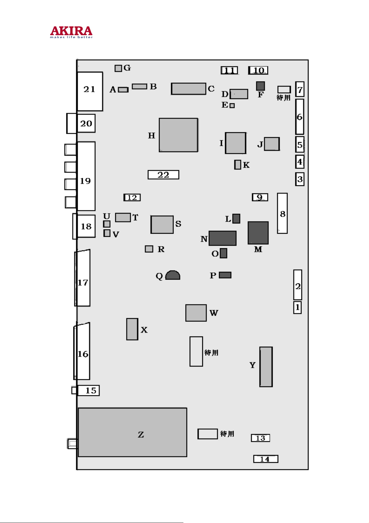
4. Position and definition of the main components and sockets on mainboard
Model No.:LCT-37CH01ST.doc
Version:1.0
56
Page 57
(1) Socket definition
S/no.
Position
Number
1 CON403 Power panel GND,GND,+12V,+12V
2 CON11 Power panel +12V,+12V,+12V,GND,GND,GND,+5V,+5V,+5V,
3 CON13 Back light control line GND,GND,back light switch control,back light brightness
4 CON14 Keyboard +3.3V、GND、KEY1、KEY2
Connecting Object Function Description
+5V,+5V
control
5 CON17 Remote control receiving
board
6 CON4 Standby
7 CON5 Standby
8 CON1 LVDS interface of line to
screen
9 CON15 I²C
10 CON12 Power panel +5V_SB , +5V_SB , GND , GND , Power supply control
11 CON13 Standby
12 CON8 Standby
13 CON9 Speaker L+,L-,R+,R-
14 CON10 Side AV board
15 J9 VGA audio signal input
16 J8 SCART2 input
17 J5 SCART1 input
18 J4 HDMI input
19 J2 HD, audio, video signal
input
20 J6 S terminal input
+3.3V、REMOTE、GND、indicator1、indicator1
21 J3 VGA input
22 CON2 Standby
Model No.:LCT-37CH01ST.doc
Version:1.0
57
Page 58

(2) Main components descriptions
S/no.
A
B
C
D
E
F
G
H
I
J
K
L
M
N
O
P
Q
R
S
T
U
V
Position
number
U16 AT24C02BN-10SU-1.8 EEPROM
U14 74LVC14AD VGA line and field synchronizing signal shaping
U2 IS42S32200C1-6TL 2MX32bits SDRAM, used for video signal access
U3 AT24C64A-10PU-2.7 EEPROM
U8 TCM809SENB713 MCU reset IC
U31 PI5C3306LE I²C bus switcher for program upgrading
U1 SVP-CX32LF
U5 SST39VF040-70-4C-NHE
U4 T5BS4-9999 MCU,mainly control IC
U6 74ALVC573PW
U18、U21、U22 AZ1117H-1.8TRE1 3.3V to 1.8V DC-DC Converter
U20 AZ1084S-3.3TRE1 5V to 3.3V DC-DC Converter
U19 、U24 AZ1117H-3.3TRE1 5V to 3.3V DC-DC Converter
U23 AZ78L08ZTR-E1 12V to 8V DC-DC Converter
U26 CS4344-CZZ HDMI digital audio decoding and D/A conversion
U30 ANX9011L HDMI decoding, HDTV video/audio reproduction
U25 AT24C02BN-10SU-1.8 EEPROM
U28、U29 Rclamp0514M.TBT HDMI signal ESD protective device
U35 STV-8217 Sound Processor
U9 74HCT4052D AV input sound passage switcher
U33 TDA8944J 2X7W Sound Amplifier(BTL Output)
U15 JS-6H2/121 Tuner
Component Function Description
Video decoding, image processor, A/D and D/A
conversion
Flash MEMORY , storing whole machine control
program
Address latch,for latching and extending the address
line
Model No.:LCT-37CH01ST.doc
Version:1.0
58
Page 59

5. Waveforms at key points
(1)RF inputting color bar signal, Composite Video Signal waveform at pin 14 of tuner U15, the waveform at pin 169 of U1
(SVP-CX32LF) is alike:
(2)
RF inputting color bar signal, I²C bus clock signal SDA, pin 5, 6 of U31, pin 6 of U16, pin 39 of U35, pin 58 of U4, pin 40 of
U30, pin 57 of U1, pin 4 of tuner U15:
Model No.:LCT-37CH01ST.doc
Version:1.0
59
Page 60

RF inputting color bar signal, I²C bus clock signal SDA, pin 2, 3 of U31, pin 5 of U16, pin 40 of U35, pin 57 of U4, pin 39
(3)
of U30, pin 58 of U1, pin 5 of tuner U15:
(4)RF inputting grey signal, Composite Video Signal waveform at pin 14 of tuner U15, the waveform at pin 169 of U1
(SVP-CX32LF) is alike:
Model No.:LCT-37CH01ST.doc
Version:1.0
60
Page 61

(5)RF inputting white signal, SIF Signal waveform at pin 11 of tuner U15, and waveform at pin 73 of sound effect processing
IC Stv-8217:
(6)RF inputting white signal, and inputting sound signal with 1KHz frequency, inductance waveforms at pin 28, 29 of U35, and
waveform of L26,L27:
Model No.:LCT-37CH01ST.doc
Version:1.0
61
Page 62

(7)Inputting sound signal with 1KHz frequency, with the processing of U33 and power amplifier TDA8944J, waveform at pin 1,
4, 14, 17 of U33, and waveform at CON13 speaker and CON14earphone output interfaces:
Model No.:LCT-37CH01ST.doc
Version:1.0
62
Page 63

TTRROOUUBBLLEE SSHHOOOOTTIINNGG
1.Failure phenomenon:The picture is normal,but OSD has line in it.
The reason and the processing:Check the pin of U2 and pin 80-160 of U1 for pseudo
soldering, and have pseudo soldering touched up.
2.Failure phenomenon:There is sound but no picture; there is no OSD when start up; and
the back light is bright.
The reason and the processing:Check the connecting line to screen, and have it
connected well.
3.Failure phenomenon:There are no picture, no sound, and no snow flower dot in TV
mode, but AV is normal.
The reason and the processing:Check the tuner and its peripheral circuits (including bus
and power supply). If the peripheral circuits work well but there is no output from tuner,
then the tuner must be failure.
4.Failure phenomenon:LCD television cannot be controlled(including no starting up with
red light on, remote control and local key having no effect, etc).
The reason and the processing:LCD television has crash phenomenon, restart after
power off.
5.Failure phenomenon:+5V_SB voltage has output, but there are no picture, no sound,
and back light and indicating light are not on.
The reason and the processing:Check other groups of voltage; if they have no outputs,
then check Flash to find if it is installed well or damaged; if Flash is OK, find out that if the
power supply and output voltage of U4 works well.
Model No.:LCT-37CH01ST.doc
Version:1.0
63
Page 64

Listing of Repair and Easily Damaged Parts
This listing of maintenance and repair parts are presented for reference only, modification
of parameters will not be informed. For accurate models or specifications, please consult
the newest data of our company. (32 inches series is taking as example)
Number Name Part code Part number Print plate number
Proportion
of
easy damage
(‰)
1. Panel frame JUG6.116.623
2. Back cover JUG6.116.624 0.1
3. Mount part JUJ7.356.005 0.1
4.
Mainboard part JUG6.690.106
Remote receiving
5.
board part JUG6.695.028
6.
Keyboard part JUG6.694.029
7.
Inner power module FSP205-5E01 Inner power module
8.
LCD screen V320B1-L04 LCD screen
9. Electronic tuner JS-6H2/121 Electronic tuner 1
10. Electronic tuner CDT-6GPL22-00 Electronic tuner 1
11. Dynamic speaker
12. Dynamic speaker
Remote control
13.
emitter
GK23J2
YDT613-A9-10W-8
Ω
YDG52-A3-10W-8
Ω
Print plate
JUG7.820.015 1
Print plate
JUG7.820.016 0.5
Print plate
JUG7.820.017 0.5
Dynamic speaker 2
Dynamic speaker 2
Remote control emitter 1
0.1
5
0.1
Model No.:LCT-37CH01ST.doc
Version:1.0
64
Page 65
r
r
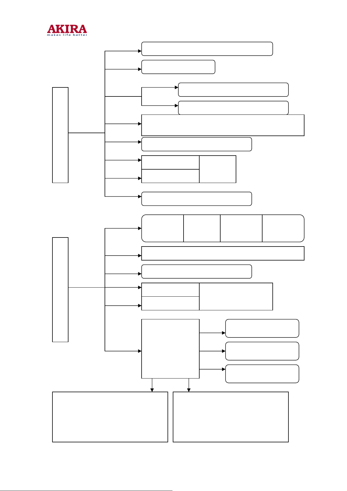
FFaaccttoorryy MMooddee SSeettttiinngg
1. Enter factory menu
Power on TV set, and make LCD at working state:
① Press 【MUTE】 key on remote control;
② Press “MENU” key on remote control, and switch to “SOUND” option with 【V+】,【V-】
key;
③ Move cursor to “Balance” option with 【P+】,【P-】key to enter setting status;
④ Press number key “3”、“1”、“3”、“8”on remote control to enter password.
Entering factory mode is then finished. Press【Display】key to quit factory mode.
⑴ Factory menu display is presented like bellow:
chassis:Ls01
Jul 29 2006 23:25:16
Version:LsE01-M32-V1.05WL
I²C off
Clear E²PROM
Panel Control
Factory Setting
System Control
Min/Max CONTROL
White Balance
Hotel Option
E²PROM Edit
Register Edit
“chassis:LS01”is the model number of local module,“Jul 29 2006 23:25:16”is the latest
Notes:
upgrading time for software, and“Version:LSE01-M32-V1.05WL”is the version number of current
software.
(2)The detailed setting items are given bellow:
Contents of first page:
Setting Item Setting Content Setting Method
IIC Off
Clear EEPROM
Panel Control
Factory Setting Factory Setting
System Control System Control
Min/Max Control
White Balance
Hotel Option Hotel mode
E²PROM Edit
Register Edit Register No setting
Stop I²C bus
communication
E²PROM
initialization
Screen back light
brightness control
Analog setting of picture
and sound
White balance
setting
E²PROM data
editing
“OK”or“V+”,“V-”key
Press “OK”key first,then
press “V-”key
Press “V+”,“V-”keys to ente
submenu
Press “V+”,“V-”keys to ente
submenu
Press “V+” key to enter
submenu
Press “V+” key to enter
submenu
Press “V+” key to enter
submenu
Press “V+” key to enter
submenu
No setting
Remark
Used for updating
program
Only done in first
setting station
Only set sub
brightness
Bri Mid
Used for hotel TV
Use 【P+】and 【P-】keys on remote control to make up or down option, and use【V+】
and【V-】keys to set.
Model No.:LCT-37CH01ST.doc
Version:1.0
65
Page 66
Contents of sub pages:
Panel Control
Setting Item
LVDS Mapping 0x09 Polarity of LVDS signal
Backlight 100 Back light brightness value 1
SavePower1 50 Back light brightness value 2
SavePower2 30 Back light brightness value 3
BL-invisible Off
Factory Setting
Setting Item Setting Value Remark
Balance -50_0_50
Volume 0_10_20…_100 Fast setting of volume,each step is 10
IIS On/Off Preset sound decoding IC of HDMI
Def Country Other Default country
RTC En On/Off Show real time clock or not
CANAL-Visual On/Off Open Canal+ function to user or not
System Control
Setting Item Setting Value Remark
Default Lang English Default OSD language SSC
L/L’ AGC 5 L/L’ sound AGC Delta 0
OverModulation On/Off OverModulation switch Positive 6
PreScl SCART 8 SCART L/R input amplitude preamplifing Negative 6
PreScl AM 12 AM_MONO IF preamplifing Write
PreScl FM 12 FM_MONO IF preamplifing
PreScl NICAM 19 NICAM sound IF preamplifing
EQ-invisible Off
ATS Off Program auto sequencing switch
Logo Off Starting blue background LOGO switch
Logo Edit AKIRA
Logo Color Logo Color Modified according to user’s require
Setting
Value
Remark
Show SavePower mode in menu or not
(ON:not show;OFF:show)
Fast check of the balance characteristic of L/R
sound channel
Equalizer switch , Off is 5 section
equalization,On is high/low pitch setting
LOGO display contents ,“ V+ ”、“ V- ” for
choosing setting position,,“P+”、“P-”for
choosing letter,including 52 English big/small
letters together
Setting
Item
Setting
Value
Model No.:LCT-37CH01ST.doc
Version:1.0
66
Page 67

Min/Max Control
Setting Item Setting Value Setting Item Setting Value
Con Min 30H Vol Min 00H
Con Mid 70H Vol Mid 1 01H
Con Max A2H Vol Mid 2 14H
Bri Min 00H Vol Mid 3 28H
Bri Mid 8DH Vol Mid 4 4BH
Bri Max A0H Vol Max 64H
Col Min 00H Tre Min 00H
Col Mid 40H Tre Mid 30H
Col Max 70H Tre Max 60H
Tnt Min 20H Bas Min 00H
Tnt Mid 80H Bas Mid 30H
Tnt Max E0H Bas Max 60H
Shp Min 00H
Shp Mid 60H
Shp Max A0H
White Balance
Normal Warm
R Gain 7DH R Gain 7DH
G Gain 80H G Gain 80H
B Gain 9AH B Gain 9AH
R Offset 80H R Offset 84H
G Offset 80H G Offset 80H
B Offset 74H B Offset 74H
Cool
R Gain 7DH
G Gain 80H
B Gain 9AH
R Offset 80H
G Offset 80H
B Offset 90H
Hotel Option
Setting Item
Hotel Mode Enable No Hotel mode presetting(Yes for Hotel Mode,No for normal TV mode)
Force Pos 1 Forced program number
Force Video ext1 Forced AV input terminal
Disable Keypad No Open local key function or not
Disable Remote No Open remote receiving function or not
Disable Setup Menu No Open “setting” in OSD menu or not
Setting
Value
Remark
Notes:
Model No.:LCT-37CH01ST.doc
Version:1.0
67
Page 68

A. In“Min/Max CONTROL” setting item, “Bri Mid”item is used to set sub brightness of
picture;
B. White balance needs to be set in “Normal”mode;
C. Set CLEAR E²PROM will clear the memory data, So do not set it unless it is needed;
other setting items do not need setting.
2. Setting method of factory menu
⑴ Choose setting item
Operators can choose setting item orderly with【P+】and【P-】key, font having background
display represents the item has been chosen. Press【V+】key to enter sub directory. Use
【P+】and 【P-】keys on remote control to make up or down option, and use【V+】and
【V-】keys to set.
(2)All the menu functions are opened in factory mode, item checking and effect testing
can be done by using menu if it is needed.
(3)Switching TV program number in factory mode can be done by directly pressing the
number key. Press【MENU 】key to back to the parent of working directory, press
【DISPLAY】key to quit factory mode.
Model No.:LCT-37CH01ST.doc
Version:1.0
68
Page 69

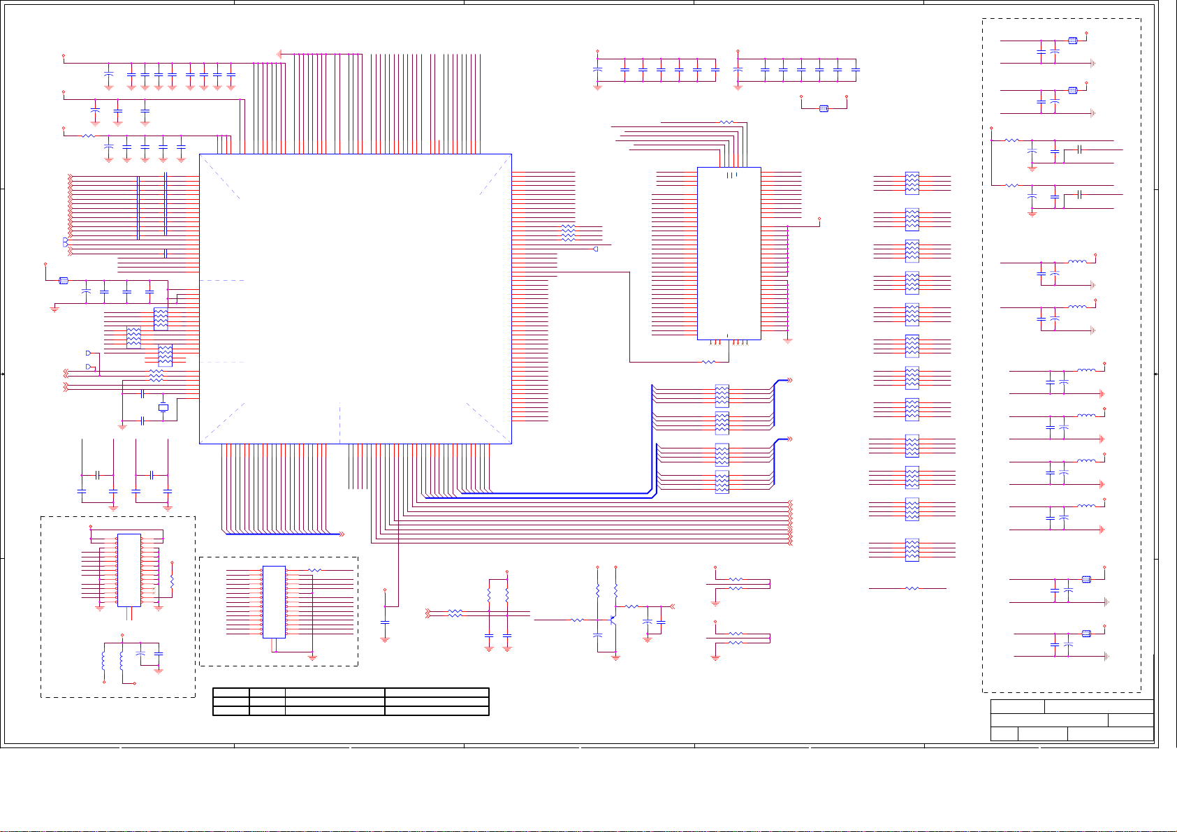
APPENDIX
LS01 module Schematic Diagram
( Sample Model: LCT-32CH01ST )
Model No.:LCT-37CH01ST.doc
Version:1.0
69
Page 70

5
4
250mm
3
2
1
IR_Key
12V
PWOR SUPPLY
5V
LVDS
512Kx8
D D
ROM
For
Europe
24bit
2Mx32
SDRM
Market
Sil9011
C C
HDMI
I2S
VGA
Y/C
SVIDEO
T5BS4
-9999
74HC573
SVP_CX32
Y C,FS2
CVBS1,RGB,FS1,FB1
Y1Pb1Pr1
Y1Pb1PR1/CVBS/L3R3/L5R5
L3
Y1
IR_Key
Pb1
L5
R3
Pb1
CVBS
250mm
SPEAKER
LA4663
140mm
L1R1
L3R3
SCART1
R5
12V
ST82X7
PT2314
L2R2
4052
SCART2
PWOR SUPPLY
TUNER
L4R4
PC_AUDIO
5V
LVDS
512Kx8
B B
ROM
For
74HC573
T5BS4
-9999
SPEAKER
LA4663
140mm
2Mx32
SDRM
Asia
&USA
Sil9011
24bit
I2S
Market
A A
VGA
HDMI
5
SVIDEO
4
SVP_CX32
Y/C
Y1Pb1Pr1
Y1Pb1PR1/CVBS/L3R3/L5R5
L3
Y1
Y C,FS2
CVBS,Y2Pb2Pr2
L5
R3
Pb1
Pr1
CVBS
L1R1
L3R3
Y2Pb2PR2/CVBS2/L1R1/L4R4
R5
3
R1
Y2L1Pb2L4Pr1
ST82X7
PT2314
L2R2
4052
R4
CVBS
L4R4
TUNER
PC_AUDIO
2
Title
LS01 Chassis
Schematict Name Rev
Sheet
Size
A3
28
Date:
of
Friday, August 18, 2006
1
Rev 1.0
Page 71
5
CX_VD18
SC1_CVBS5
CX_VD33
3.3V POWER
FOR LVDS
CX_CVBS_OUT25
CX_CVBS_OUT15
PC_HSIN5
PC_VSIN5
CX_VD33
CX_VDDM
R2 20m,1%
TV_MAIN5
Y5
SC1_G5
SV_Y_MP5
PC_GIN5
PR5
SC1_R5
SC2_Y5
PC_RIN5
SV_C_MP5
PB5
SC1_B5
PC_BIN5
TP4
TP5
SC1_FB5
SC2_C5
FB4
150_Ohm_600mA
12
CX_LVDS_VSS
TP7
TP6
LAYOUT: Place xtal
circuit as compact
and close to chip
as possible
CX_VREFP_2
TD1+
TD1TCLK1+
TCLK1TC1+
TC1-
TB1TA1+
TA1-
+
C59
10uF
C71
0.1uF_DNS
C75
0.1uF
PVDD
D D
C C
B B
LVDS INTERFACE
A A
C17
10uF
+
C28
10uF
C31
10uF
CX_LVDS_VDD
C60
0.1uF
TCLK1TCLK1+
TA1-
TA1+
TB1-
TB1+
TC1TC1+
TD1TD1+
C76
0.1uF
FB7
150_Ohm_3000mA
5V
CX_VD18_LOCAL
+
C20
C18
C19
0.1uF
0.1uF
0.1uF
C29
C30
0.1uF
0.1uF
CX_VDDM_LOCAL
+
C32
C33
0.1uF
0.01uF
0.1uF
C40 0.1uF
C42 0.1uF
C44 0.1uF
C49 0.1uF
C51 0.1uF
C53 0.1uF
C55 0.1uF
CX_VREFP_1
CX_VREFN_1
CX_VREFP_2
CX_VREFN_2
C61
C62
0.1uF
0.1uF
RN35 0x4
1
2
3
RN34 0x4
4
1
8
2
7
3
6
4
5
R10 75
R11 75
R12 100 C65
C67 20pF
Y1
14.318MHz
C68 20pF
C72
0.1uF_DNS
CX_VREFN_2
CX_VREFP_1
C77
0.1uF
CON1
12
34
56
78
910
11 12
13 14
15 16
17 18
19 20
21 22
23 24
25 26
27 28
29 30
GND
GND
DF13 15P*2-1.25mm
31
32
PVDD
+
C91
FB8
150_Ohm_3000mA
12V
5
C21
0.1uF
C34
0.01uF
C39 0.1uF
C41 0.1uF
C43 0.1uF
C46 0.1uF
C50 0.1uF
C52 0.1uF
C54 0.1uF
C56 0.1uF
8
7
6
5
RN33 0x4
1
2
3
4
CX_VREFN_1
C78
0.1uF
PVDD
C92
100uF/16V
C22
0.01uF
C35
8
7
6
5
R14
NC
0.1uF
C23
C25
C24
0.01uF
0.01uF
0.01uF
96
119
136
98
108
134
146
VDDM
VDDM
VDDM
VDDM
169
CVBS1
180
Y_G1
181
Y_G2
182
Y_G3
183
PC_G
188
PR_R1
189
PR_R2
190
PR_R3
191
PC_R
192
C
196
PB_B1
197
PB_B2
198
PB_B3
199
PC_B
171
FS1
170
FS2
173
FB1
172
FB2
174
VREFP_1
175
VREFN_1
184
VREFP_2
185
VREFN_2
52
LVDS_VDDP
38
PLL_GND
39
PLL_VCC
47
LVDSGND
46
LVDSVCC
43
TCLK1M
42
TCLK1P
51
TA1M
50
TA1P
49
TB1M
48
TB1P
45
TC1M
44
TC1P
41
TD1M
40
TD1P
162
CVBS_OUT2
163
CVBS_OUT1
157
TESTMODE
158
AIN_HS
159
AIN_VS
205
XTALI
204
XTALO
DP0
DP1
DP2
37363534333231302926252422211817161514111098755575860596263615684868545236646566676869707183828180797877
DP1
DP2
DP3
DP0
DP0
DP1
DP2
DP3
DP4
DP5
DP6
DP7
DP8
DP9
DP10
DP11
DP12
DP13
DP14
Digital Input
Connector
GPIO1
160
VDDC
VDDC
VDDC
VDDC
VDDH
VDDH
VDDC
Aanalog I/OLVDSMISC
DP3
DP4
DP5
DP6
DP7
DP8
DP9
DP10
DP11
DP6
DP10
DP4
DP5
DP8
DP7
DP9
DP11
DP12
CON2
12
34
56
78
910
11 12
13 14
15 16
17 18
19 20
21 22
23 24
25 26
27 28
29 30
GND
0.5MM FPC CONNECTOR_DNS
31
Pin No.
535474
121327
28
VSSC
VSSC
VSSC
VDDC
VDDC
VDDC
DP12
DP13
DP14
DP15
DP16
DP17
DP18
DP17
DP18
DP16
DP15
DP14
DP13
DP19
R13 33
GND
32
1 (HIGH)
MPU in A/D Multiplix Mode
Use Rising Edge of WR# to latch data
97
120
13799110
7572201973
161
VSSC
VSSC
VSSC
VSSC
VSSH
VSSC
Power / Ground
SVP-CX32_208
DP19
DP20
DP21
DP22
DP23
DP20
DP21
DP22
DP23
DP_CLK
DP_HS
DP_VS
DP_DE_FLD
DP23
DP22
DP21
DP20
DP19
DP18
DP17
DP16
DP15
4
135
VSSH
VSSM
VSSM
VSSM
PWM0
SCL
SDA
CX_PWM0
CX_SCL
CX_SDA
DP[0..23] 8
4
CX_AVDD3_ADC1
CX_AVDD3_ADC2
CX_PLF2
CX_PAVDD
CX_PAVDD1
CX_PAVSS1
CX_PAVDD2
CX_PAVSS2
CX_PAVSS
CX_MLF1
147
168
195
202
203
208
206
20731
2
PLF2
MLF1
VSSM
PAVSS
PAVSS1
PAVSS2
PAVDD1
PAVDD2
AVDD3_ADC1
AVDD3_ADC2
CPU interfaceDigital out
GPIO0
GPIO1
WR#
RD#CSINTN
ALE
RESET
V5SF
DP_HS
DP_VS
CX_GPIO0
CX_GPIO1
8051_ALE
DP_HS
8051_RD#
DP_VS
8051_CS2CX
8051_WR#
DP_CLK
CX_INT#
RESET_H
5V_SB
I2C Slave Address is
fixed to 0x7e/0x7f
3V_SDA4,7,8
3V_SCL4,7,8
C83
0.1uF
0 (LOW)Pin Name
MPU in A/D Separate ModeGPIO0
Use Falling Edge of WR# to latch data
CX_PDVSS
201
PAVDD
DP_CLK
DP_DE_FLD
CX_PDVDD
PDVSS
DP_DE_FLD
8051_A0
200
PDVDD
ADDR0
ADDR1
8051_A1
CX_AVDD_ADC18051_A2
177
AVDD_ADC1
ADDR2
CX_AVDD_ADC2
186
193
AVDD_ADC2
ADDR3
8051_A4
8051_A3
CX_AVSS_ADC4
CX_AVSS_ADC1
CX_AVSS_ADC2
CX_AVSS_ADC3
CX_AVDD_ADC4
176
187
194
178
AVSS_ADC1
AVSS_ADC2
AVSS_ADC3
AVDD_ADC3
AVDD_ADC4
ADDR4
ADDR5
ADDR6
ADDR7
A_D0
8051_A7
8051_A6
8051_A5
8051_AD0
8051_AD1
R22 10
R23 10
CX_AVDD3_OUTBUF
179
AVSS_ADC4
A_D1
8051_AD2
CX_AVSS_OUTBUF
CX_AVDD3_BG_ASS
165
164
AVSS_OUTBUF
AVDD3_OUTBUF
A_D2
A_D3
8051_AD3
8051_AD4
4.7K_DNS
68pF_DNS
CX_AVSS_BG_ASS
167
166
AVSS_BG_ASS
AVDD3_BG_ASS
A_D4
A_D5
8051_AD5
R19
C86
MA10
MA11
DQM0
DQM1
DQM2
DQM3
RAS#
CAS#
CLKE
CS0#
SDRM
MD10
MD11
MD12
MD13
MD14
MD15
MD16
MD17
MD18
MD19
MD20
MD21
MD22
MD23
MD24
MD25
MD26
MD27
MD28
MD29
MD30
MD31
A_D6
A_D7
76
8051_AD6
8051_AD7
MA0
MA1
MA2
MA3
MA4
MA5
MA6
MA7
MA8
MA9
BA0
BA1
WE#
MCK
MD0
MD1
MD2
MD3
MD4
MD5
MD6
MD7
MD8
MD9
CX_VD33
R20
4.7K_DNS
CX_SDA
CX_SCL
C87
68pF_DNS
CX_MA0A
124
CX_MA1A
123
CX_MA2A
122
CX_MA3A
121
CX_MA4A
118
CX_MA5A
117
CX_MA6A
116
CX_MA7A
115
CX_MA8A
114
CX_MA9A
113
CX_MA10A
125
CX_MA11
126
CX_DQM0
156
CX_DQM1
133
CX_DQM2
109
CX_DQM3
87
CX_BA0A
128
CX_BA1
127
CX_RAS#A
130
CX_CAS#A
131
CX_WE#A
132
CX_CLKEA
112
CX_CS0#
129
CX_MCLKA
111
DQ15
155
DQ14
154
DQ13
153
DQ12
152
DQ11
151
DQ10
150
DQ9
149
DQ8
148
DQ7
145
DQ6
144
DQ5
143
DQ4
142
DQ3
141
DQ2
140
DQ1
139
DQ0
138
DQ23
107
DQ22
106
DQ21
105
DQ20
104
DQ19
103
DQ18
102
DQ17
101
DQ16
100
DQ31
95
DQ30
94
DQ29
93
DQ28
92
DQ27
91
DQ26
90
DQ25
89
DQ24
88
U1
SVP_CX32
CX_PWM0
R5 15
R6 15
R7 15
R8 15
8051_AD[0..7]
8051_A[0..7]
R24 0
3
10uF_DNS
3
+
C4
C3
22uF
C5
C6
0.1uF
0.1uF
0.1uF
SDRAM DECOUPLING CAPACITORS
DQM1
DQM0
DQM2
DQM3
TP1
DP_DE_FLD
DP_CLK
DP_VS
DP_HS
RESET_H
8051_ALE
CX_INT#
8051_CS2CX
8051_RD#
8051_WR#
5VCX_VD33 3.3V_SB
R17
R16
4.7K
1.2K
R21
1K
Q1
C84
+
100uF
MMBT3906
+
C88
DQM0
DQM1
DQM2
DQM3
CX_MD15
CX_MD14
CX_MD13
CX_MD12
CX_MD11
CX_MD10
CX_MD9
CX_MD8
CX_MD7
CX_MD6
CX_MD5
CX_MD4
CX_MD3
CX_MD2
CX_MD1
CX_MD0
CX_MD23
CX_MD22
CX_MD21
CX_MD20
CX_MD19
CX_MD18
CX_MD17
CX_MD16
CX_MD31
CX_MD30
CX_MD29
CX_MD28
CX_MD27
CX_MD26
CX_MD25
CX_MD24
C7
0.1uF
CX_BA0
CX_WE#
CX_CAS#
CX_MCLK
CX_CS0#
8051_AD0
8051_AD1
8051_AD2
8051_AD3
8051_AD4
8051_AD5
8051_AD6
8051_AD7
8051_A0
8051_A1
8051_A2
8051_A3
8051_A4
8051_A5
8051_A6
8051_A7
BRT_CNTL 7
C85
0.01uF
C8
0.1uF
CX_MA11
CX_RAS#
CX_CLKE
C9
0.1uF
16
DQM0
71
DQM1
28
DQM2
59
DQM3
2
DQ0
4
DQ1
5
DQ2
7
DQ3
8
DQ4
10
DQ5
11
DQ6
13
DQ7
74
DQ8
76
DQ9
77
DQ10
79
DQ11
80
DQ12
82
DQ13
83
DQ14
85
DQ15
31
DQ16
33
DQ17
34
DQ18
36
DQ19
37
DQ20
39
DQ21
40
DQ22
42
DQ23
45
DQ24
47
DQ25
48
DQ26
50
DQ27
51
DQ28
53
DQ29
54
DQ30
56
DQ31
R9 0
C10
22uF
R1 0
1918172268
67
CLK
RAS
CKE
CS
NC_14
NC_21
NC_30
20
14213069707357
RN1 100x4
1
8
2
7
3
6
4
5
RN2 100x4
1
8
2
7
3
6
4
5
RN3 100x4
4
5
3
6
2
7
1
8
RN4 100x4
4
5
3
6
2
7
1
8
R15 4.7K_DNS
CX_GPIO1TB1+
R18 4.7K
3.3V_SB
R25 4.7K
CX_GPIO0
R26 4.7K_DNS
CX_VDDMCX_VDDM
CAS
NC_57
+
WE
BA0
A10/AP
NC_69
NC_70
C11
0.1uF
U2
23
2Mx32_SDRAM
A0
BA1
A1
A2
A3
A4
A5
A6
A7
A8
A9
VDD
VDD
VDD
VDD
VDDQ
VDDQ
VDDQ
VDDQ
VDDQ
VDDQ
VDDQ
VDDQ
VSSQ
VSSQ
VSSQ
VSSQ
VSSQ
VSSQ
VSSQ
VSSQ
VSS
VSS
VSS
VSS
NC_73
uP_AD0
uP_AD1
uP_AD2
uP_AD3
uP_AD4
uP_AD5
uP_AD6
uP_AD7
uP_A0
uP_A1
uP_A2
uP_A3
uP_A4
uP_A5
uP_A6
uP_A7
2
C13
0.1uF
uP_AD[0..7] 4
uP_A[0..7] 4
DP_DE_FLD 8
DP_CLK 8
DP_VS 8
DP_HS 8
RESET_H 4
8051_ALE 4
CX_INT# 4
8051_CS2CX 4
8051_RD# 4
8051_WR# 4
C14
0.1uF
FB3
1 2
150_Ohm_600mA
CX_VDDM
C15
C16
0.1uF
0.1uF
CX_VDDMCX_VD33
CX_VL18
R3 22
RN22 100x4
1
2
3
4
RN23 100x4
1
2
3
4
RN21 100x4
1
2
3
4
RN24 100x4
1
2
3
4
RN20 100x4
1
2
3
4
RN19 100x4
1
2
3
4
RN18 100x4
1
2
3
4
RN17 100x4
1
2
3
4
4
3
2
1
RN27 100x4
4
3
2
1
RN26 100x4
4
3
2
1
RN25 100x4
RN28 100x4
1
2
3
4
R269
CX_MD0
8
CX_MD1
7
CX_MD2
6
CX_MD3
5
CX_MD4
8
CX_MD5
7
CX_MD6
6
CX_MD7
5
CX_MD8
8
CX_MD9
7
CX_MD10
6
CX_MD11
5
CX_MD12
8
CX_MD13
7
CX_MD14
6
CX_MD15
5
CX_MD16
8
CX_MD17
7
CX_MD18
6
CX_MD19
5
CX_MD20
8
CX_MD21
7
CX_MD22
6
CX_MD23
5
CX_MD24
8
CX_MD25
7
CX_MD26
6
CX_MD27
5
CX_MD28
8
CX_MD29
7
CX_MD30
6
CX_MD31
5
CX_BA0
5
CX_RAS#
6
CX_CAS#
7
CX_WE#
8
CX_MA7A
5
CX_MA8A
6
CX_MA9A
7
CX_CLKEA
8
CX_MA3A
5
CX_MA4A
6
CX_MA5A
7
CX_MA6A
8
CX_MA10
8
CX_MA0
7
CX_MA1
6
CX_MA2
5
0
CX_MCLKCX_MCLKA
R4 22
DQ15
DQ14
DQ13
DQ12
DQ11
DQ10
DQ9
DQ8
DQ7
DQ6
DQ5
DQ4
DQ3
DQ2
DQ1
DQ0
DQ23
DQ22
DQ21
DQ20
DQ19
DQ18
DQ17
DQ16
DQ31
DQ30
DQ29
DQ28
DQ27
DQ26
DQ25
DQ24
CX_BA0A
CX_RAS#A
CX_CAS#A
CX_WE#A
CX_MA7
CX_MA8
CX_MA9
CX_CLKE
CX_MA3
CX_MA4
CX_MA5
CX_MA6
CX_MA10A
CX_MA0A
CX_MA1A
CX_MA2A
C12
0.1uF
CX_MA0
25
CX_MA1
26
CX_MA2
27
CX_MA3
60
CX_MA4
61
CX_MA5
62
CX_MA6
63
CX_MA7
64
CX_MA8
65
CX_MA9
66
CX_MA10
24
1
15
29
43
3
9
35
41
49
55
75
81
6
12
32
38
46
52
78
84
44
58
72
86
1
CX_PDVDD
CX_PDVSS
CX_PAVDD
CX_PAVSS
C37
10uF
C47
10uF
CX_AVDD3_ADC1
CX_AVDD3_ADC2
CX_AVDD_ADC1
CX_AVSS_ADC1
CX_AVDD_ADC2
CX_AVSS_ADC2
CX_AVDD_ADC3
CX_AVSS_ADC3
CX_AVDD_ADC4
CX_AVSS_ADC4
3.3V POWER FOR CVBS
OUTPUT BUFFER
CX_AVDD3_OUTBUF
CX_AVSS_OUTBUF
CX_AVDD3_BG_ASS
CX_AVSS_BG_ASS
FB1
1 2
+
150_Ohm_600mA
C2
C1
10uF
0.1uF
FB2
1 2
+
150_Ohm_600mA
C27
C26
10uF
0.1uF
+
C36 2700pF
C38
0.1uF
+
C45 2700pF
C48
0.1uF
3.3V POWER
FOR ADC
L1
2.2uH_1210
+
C58
C57
10uF
0.1uF
L2
2.2uH_1210
+
C64
C63
10uF
0.1uF
1.8V POWER
FOR ADC
+
C66
10uF
0.1uF
+
C69
C70
0.1uF
10uF
+
C74
C73
10uF
0.1uF
+
C80
C79
10uF
0.1uF
+
C81
C82
0.1uF
10uF
3.3V POWER FOR
ADC
+
C89
C90
0.1uF
10uF
CX_VL18
CX_VL18
L3
2.2uH_1210
L4
2.2uH_1210
L5
2.2uH_1210
L6
2.2uH_1210
FB5
1 2
150_Ohm_600mA
FB6
1 2
150_Ohm_600mA
CX_PAVDD1
CX_PAVSS1
CX_PAVDD2
CX_PAVSS2
CX_VD33
CX_VD33
CX_MLF1
CX_PLF2
CX_VA18
CX_VA18
CX_VA18
CX_VA18
CX_VD33
CX_VD33
POWER FOR CX32
Title
38
of
1
LS01 Chassis
Date:
Friday, August 18, 2006
Rev 1.0
Schematict Name Rev
Size
Sheet
2
CX_AVDD_ADC3
Page 72
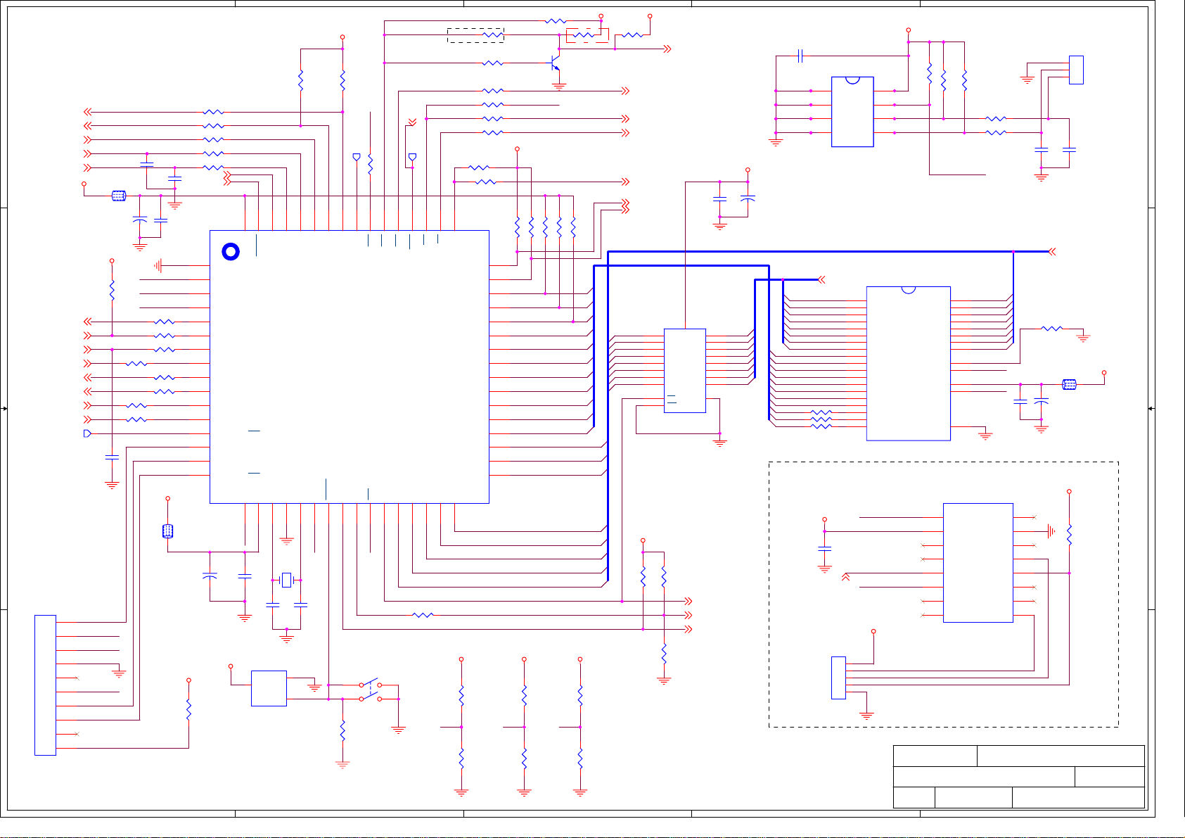
5
R28
4.7K
C402
0.1uF
SDAE
SCLE
C99
0.1uF
P92
3.3V_SB
12
R35 100
R38 100
R41 100
R42 100
R44 100
SC1_FS5
C404
SC2_FS5
0.1uF
U4
1
AVSS
2
P70/TA0IN
3
P71/TA1OUT
4
P72/TA3OUT
5
P73/TA4IN
6
P74/TA5OUT
7
P80/TB0IN0/INT5
8
P81/TB0IN1/INT6
9
P82/TB0OUT0
10
P83/TB0OUT1
11
P90/TXD0
12
P91/RXD0
13
P92/SCLK0/cts0
14
P93/TXD1
15
P94/RXD1
16
P95/SCLK1/cts1
FB11
150_Ohm_600mA
+
C104
10uF
5V_SB
R67
0
60
61
62
63
64
AVCC
P53/AN3/ADTRG
AM0
DVCCX2DVSSX1AM1
171819202122232425262728293031
AM0
C105
0.1uF
3.3V_SB
U8
TCM809SENB713
3
VCC
RESET#
C10618pF
GND
P52/AN2
Y2
27MHz
P50/AN0
P51/AN1
C10718pF
1
2
D D
C C
B B
A A
BKLT_CNTL7
REMOTE_3V7
HDMI_HOTPLUG8
CON4
TJC3_10A
3V_SDA3,7,8
3V_SCL3,7,8
CX_INT#3
KEYB7
KEYA7
3.3V_SB
FB9
150_Ohm_600mA
1 2
C98
10uF
3.3V_SB
R216
4.7K
SW185
RX_INT#8
LED_R7
LED_G7
SCDT8
TP9
C102
100pF
10
RD#
9
CPU_RST
8
7
6
WR#
5
4
3
2
1
E_PAGE
R253 0
R53 100
R54 1K
R226 100
R55 100
R56 100
R227 100
R228 100
5
4
3.3V_SB
R29
4.7K
PS
TP2
R4322R
P60
55
56
57
58
59
p42/CS2
P60/SCK
P63/INT0
P62/SI/SCL
P61/SO/SDA
T5BS4-9999
RESET
P96/XT1
P97/XT2
NMI
CPU_RST
K15 NC
1 3
2 4
R68
100K
4
NMI
AM1
54
P41/CS1
ALE
P32
TP3
4
P32
WR#
52
53
P40/CS0
P32/HWR
P00/AD0
P01/AD1
R62 0
R303
100
R30 2.2K
R33 22
R34 22
R36 22
R39 22
RD#
R45 10K
R46 100
49
50
51
P30/RD
P31/WR
P25/A5/A21
P24/A4/A20
P23/A3/A19
P22/A2/A18
P21/A1/A17
P20/A0/A16
P17/AD15/A15
P16/AD14/A14
P15/AD13/A13
P14/AD12/A12
P13/AD11/A11
P12/AD10/A10
P11/AD9/A9
P10/AD8/A8
P07/AD7
P06/AD6
P05/AD5
P02/AD2
P03/AD3
P04/AD4
32
uP_AD4
uP_AD3
uP_AD2
uP_AD1
uP_AD0
3.3V_SB 3.3V_SB
R64
1K_DNS
AM0 AM1
R69
3
R301 1.2K
Q14
2SC1815M-Y
2 3
R51
R50
100K
100K
3.3V_SB
NMI
3
3.3V_SB 5Vstb
R266 2.0K
8051_CS2CX 3
8051_WR# 3
8051_RD# 3
MUTE 6
L/R_SW1 5
L/R_SW2 5
uP_AD0
uP_AD1
uP_AD2
uP_AD3
uP_AD4
uP_AD5
uP_AD6
uP_AD7
3.3V_SB
R66
1K_DNS
R71
1K
SB_PWR 7
2
D0
3
D1
4
D2
5
D3
6
D4
7
D5
8
D6
9
D7
11
LE
1
OE
U6
74ALVC573PW
R263
R61
10K
10K
R63
NC
C96
0.1uF
A[8..18]
20
19
Q0
18
Q1
VCC
17
Q2
16
Q3
15
Q4
14
Q5
13
Q6
12
Q7
10
GND
8051_ALE 3
RESET_H 3
RESET_L 6,8
uP_A0
uP_A1
uP_A2
uP_A3
uP_A4
uP_A5
uP_A6
uP_A7
3.3V_SB
+
C97
10uF
R302 4.7K
1
WE#
3.3V_SB
R47
R49
R48
100K
100K
100K
48
47
A18
46
A17
45
A16
44
A15
43
A14
42
A13
41
A12
40
A11
39
A10
38
A9
37
A8
36
uP_AD7
35
uP_AD6
34
uP_AD5
33
R65
1K_DNS
R70
1K
1K
C93 1000pF
uP_AD[0..7]
uP_A[0..7]
A8
A9
A10
A11
A12
A13
A14
A15
A16
R57 0
R58 0
A17
R59 0
A18
2
1
1
A0
A0
2
2
A1
A1
3
3
A2
A2
4 5
4 5
GND SDA
GND SDA
U3
AT24C64A-10PU-2.7
uP_A[0..7] 3
uP_A1
uP_A2
uP_A3
uP_A4
uP_A5
uP_A6
uP_A7
3.3V_SB
C103
NC
P32
CON5
NC
5x2.0mm
2
3.3V_SB
8
8
VCC
VCC
7
7
PAGE
PAGE
6
6
SCL
SCL
U5
SST39VF040-70-4C-NHE
12
A0
11
A1
10
A2
9
A3
8
A4
7
A5
6
A6
5
A7
27
A8
26
A9
23
A10
25
A11
4
A12
28
A13
29
A14
3
A15
2
A16
30
A17
1 16
A18 VSS
P60
P32
P92
4
3.3V_SB
1
2
3
4
5
Schematict Name Rev
Size
R27
R31
4.7K
4.7K
E_PAGE
13
Q0
14
Q1
15
Q2
17
Q3
18
Q4
19
Q5
20
Q6
21
Q7
22
CE
24
OE
32
VDD
31
WE
2
1 B1
5
2 B1
11
3 B1
14
4 B1
3
1 B2
6
2 B2
10
3 B2
13
4 B2
For Encrypt
Sheet
R32
4.7K
R37 100
R40 100
uP_AD0uP_A0
uP_AD1
uP_AD2
uP_AD3
uP_AD4
uP_AD5
uP_AD6
uP_AD7
PS
RD#
WE#
C100
0.1uF
U7
NC
78K0S/KY1+
VCC
/OE
GND
Title
48
of
1
SCLE
SDAE
C94
100pF
uP_AD[0..7] 3
R52
10K
FB10
150_Ohm_600mA
+
C101
10uF
3.3V_SB
16
4
1A
7
2A
9
3A
12
4A
1
S
15
8
LS01 Chassis
Date:
Friday, August 18, 2006
1
CON3
1
2
3
I2C
C95
100pF
3.3V_SB
12
R60NC
Rev 1.0
Page 73
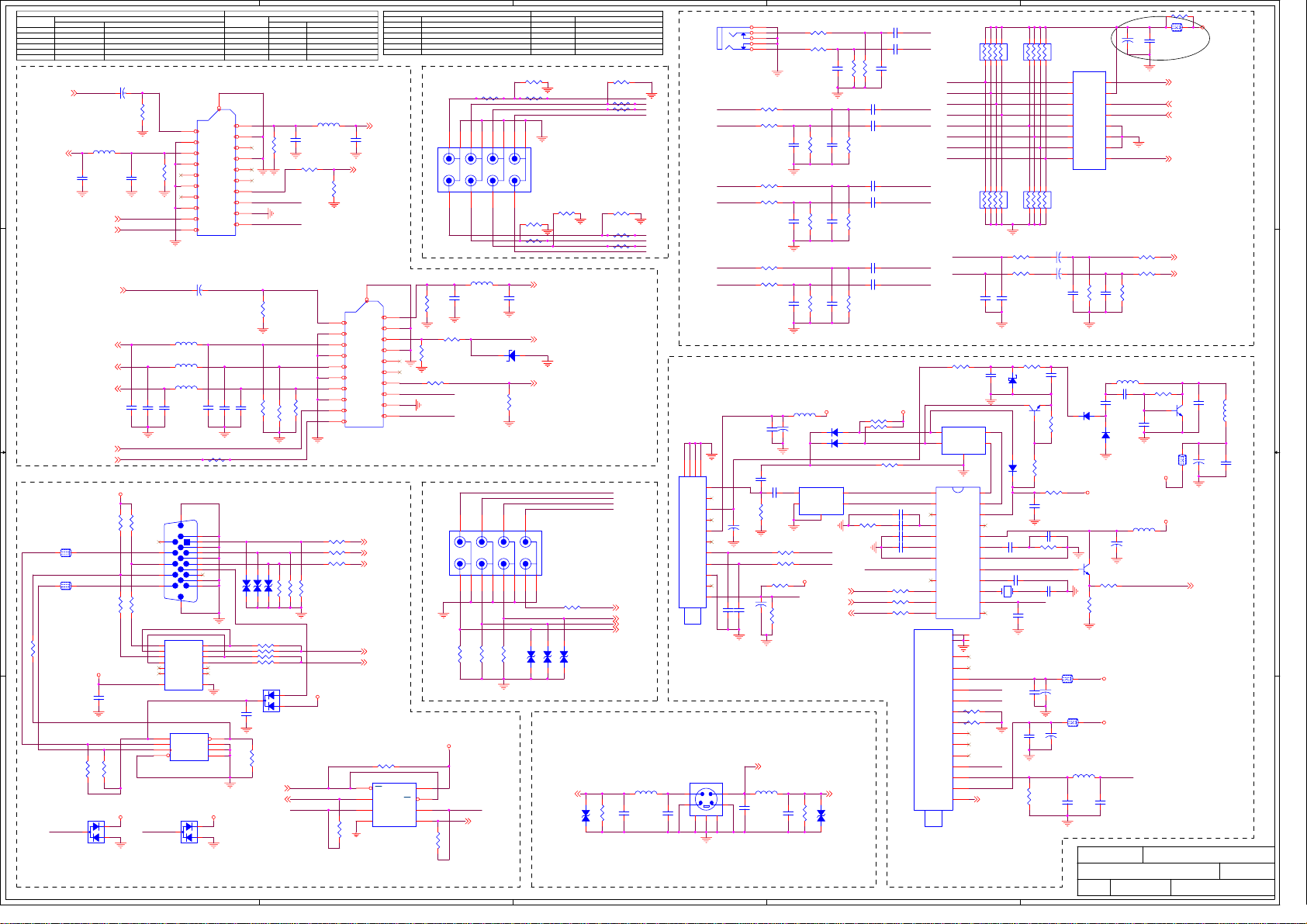
Definition In C X 3 2 Solution(Europe Market)
Name
Input Signal
CVBS INPUT
MAIN TUNER CVBS1
R/G/B INPUT
Y/Pb/Pr INPUT
SCART1
CVBS/Y/C;FS
SCART2
CVBS/Y/C
AV/SV
CX_CVBS_OUT23
D D
SC2_C3
C122
100pF
CX_CVBS_OUT13
C C
FB14
VGA_SDA_IN
1 2
150_Ohm_600mA
B B
A A
FB15
1 2
150_Ohm_600mA
R138
NC
VGA_SDAVGA_SDAVGA_SDAVGA_SDA
VGA_SCLVGA_SCLVGA_SCLVGA_SCLVGA_SCLVGA_SCL
VGA_HSIN
VGA_SCL_IN
R150
10K
3
BAV99L
5
Definition Video Signal
Input CX32 Pin
CVBS1 CVBS INPUT
PC_R
PC_GPC VGA
PC_B
PR_R1
Y_G1
PB_B1
PB_B3 PR_R2
Y_G2CVBS;R/G/B;FB;FS
FB2
PR_R3
Y_G3
C
+
C114
470uF/16V
R77
100K
L8 2.2uH
R82
C123
100pF(nc)
SC2_LOUT6
SC2_ROUT6
Full Scart And Half Scart Socket
Only For Europe Market
SC1_R3
SC1_G3
SC1_B3
C147
C148
100pF
100pF
SC1_LOUT6
SC1_ROUT6
5V_SB
R119
R118
2.0K
2.0K
R136
R137
22
22
VGA_VSIN
VGA_HSIN
5V_SB
U14
AT24C02BN-10SU-1.8
C177
0.1uF
R151
10K
5V_SB 5V_SB
D7
2
VGA_VSIN
1
5
FB1
PB_B2
FS2
19
VOUT
17
GND
15
R
13
GND
11
9
7
5
3
1
J8 scart2
+
C135 470uF/16V
L11 2.2uH
L12 2.2uH
L14 2.2uH
C149
100pF
C150
J3
1617
DB15_female
GG
6
11
11
1
7
12
12
2
8
13
13
3
9
14
14
4
10
15
15
5
1 2
1A 1Y
3 4
2A 2Y
5 6
3A 3Y
9 8
4A 4Y
11 10
74LVC14
5A 5Y
13 12
6A 6Y
GNDVCC
8
VCC
VCLK
5
SDA
NC2
6
SCL
NC1
4
GND
NC0
U16
AT24C02BN-10SU-1.8
D8
3
BAV99L
G
GND
B
GND
AOL
AOR
75
I2C Address: 1010 000x
Definition In C X 3 2 So l u t i on(Asia&USA Market)
Name
MAIN TUNER
COMPONENT1
FS1
COMPONENT2
CVBS1
AV/SV
21
20
VIN
SHIELD
18
GND
16
RGB_ST
14
GND
12
DT1
10
DT2
8
V_ST
6
AIL
4
GND
2
AIR
C152 100pF(nc)
C151 100pF(nc)
100pF(nc)
R267 0
6
1
7
2
8
3
9
4
10
5
DM1
ESD
R139 22_DNS
R140 22
R144 22_DNS
R145 22
714
C178
0.1uF
7
3
2
R256
1
0R
2
1
Definition Video Signal
Input Signal
Input CX32 Pin
R/G/B INPUT
Y_G1
Y/Pb/Pr INPUTCOMPONENT
Y/Pb/Pr INPUTPR_R2
Y_G2
PR_R3
CVBS
CVBS/Y/C
Y_G3
SC2_AV
C119
R81
100pF(nc)
75
R83 10K
R85
2K
SC2_LIN
SC2_RIN
SC1-Vout
R100
100K
SCART_RINSCART_RINSCART_RINSCART_RIN
SCART_GINSCART_GINSCART_GINSCART_GIN
SCART_BIN
R108 75
R111 75
R107 75
VGA Connect Interface
VGA_RINVGA_RINVGA_RIN
DM2
ESD
DM3
ESD
D6
3
CMPSH-3C
1: DDC
0: UPDATE
FLASH
SW184
R123 0
R124 0
R127 0
R13375
R13175
R13275
5V_SB
2
1
VGA_SDA
L7
2.2uH
PC_R
PB_B1
PB_B2
C
100pF
19
17
15
13
11
C120
9
7
5
3
1
4
Definition In C X 3 2 So lution(Europe Market)
Name
MAIN TUNER
PC VGA
COMPONENT
PC_BPC_GPC VGA
SCART1 SC1_RIN,SC1_LIN
PR_R1
SCART2
AV/SV AV/SV
SC2_Y 3
SC2_FS 4
21
20
VIN
SHIELD
VOUT
18
GND
GND
16
RGB_ST
R
14
GND
GND
12
DT1
G
10
DT2
GND
8
V_ST
B
6
AIL
GND
4
GND
AOL
2
AIR
AOR
scart1
J5
PC_RIN 3
PC_GIN 3
PC_BIN 3
PC_HSIN 3
PC_VSIN 3
Definition Audio Signal
SIF, TV_MONO
L4_IN,R4_IN
L3_IN,R3_IN
SC1_RIN,SC1_LIN,SC1_LOUT,SC1_ROUT
SC2_RIN,SC2_LIN SC2_RIN,SC2_LIN
L5_IN,R5_IN
R252
R229
R266
0
R99
75
R258 100
R101
75
R105 10K
SC1_LIN-
SC1_RIN-
13467910
2
5
L9 2.2uH
C138
100pF(nc)
2
13467910
R141
R142
75
75
5
8
D10
ZMM55C3V0
8
R143
75
12
11
R182 0
R167 0
C139
100pF
12
R106
2K
11
Component1 & AV Socket
5V_SB
R257 4.7K
U31 PI5C3306LE
1
2
3
4 5
R2540_DNS
BE1
A1
B1
GND A2
4
8
VCC
7
BE2
B2
VGA_SCL
6
R2550_DNS
5V_SCL 6,7
Definition In C X 3 2 So l u t i on(Asia&USA Market)
Name Definition Audio Signal
SIF, TV_MONO
MAIN TUNER
PC VGA
L4_IN,R4_IN
L3_IN,R3_IN
COMPONENT1
COMPONENT2
CVBS1
L5_IN,R5_IN
SCART_RIN
SCART_GIN
SCART_BIN
SC1_Vout
0
SC1_RINSC1_LINSC1_Rout
SC1_Lout
DM7
ESD
R5_IN
L5_IN
R3_IN
L3_IN
R148
75
R197
R192 0
R205 0
R211
R212 0
R210 0
C182
100pF
0
0
Component2 And
J1
CVBSout Socket
RCA4X2
Only For Asia&USA
Market
R209
SC1_CVBS 3
SC1_FB 3
SC1_FS 4
J2
RCA4X2
12
R23733
DM4
DM6
DM5
ESD
ESD
ESD
SV_C_MP3
3
0
0
AV_CVBS
5
PR 3
PB 3
Y3
L18
2.2uH
100pF_DNS
3
J10
121314
15
ET-5F2E-EF107
GND
GND
NC
NC
NC
SDA
SCL
NC
AGC
SVIDEO Socket
C183
2 1
J9
PC Audio in
L3_IN
L5_IN
R5_IN
SC2_LIN
SC2_RIN
1
2
5
3
4
R76 470
R78 470
R84 470
R86 470
R91 470
R94 470
C117
470pF
C125
470pF
C136
470pF
R72 470
R73 470
C112
470pF
R79
100K
R87
100K
R97
100K
C118
470pF
C126
470pF
C137
470pF
2
C108
LIN4-
1uF
C111
RIN4-
R74
100K
R80
R88
100K
1uF
R75
C113
100K
470pF
C115
1uF
C116
1uF
100K
C121
1uF
C124
1uF
100K
C128
SCART2_LIN-
1uF
C130
SCART2_RIN-
1uF
R98
LIN3-
RIN3-R3_IN
LIN5-
RIN5-
LIN4LIN3LIN5SCART2_LINRIN4RIN3RIN5SCART2_RIN-
SC1_LIN-
SC1_RIN-
C133
1000pF
876
123
876
123
5
RN5
10K X 4
4
5
RN7
10K X 4
4
R89 220
R92 220
C134
1000pF
876
123
876
123
5
4
5
4
C127
10uF/16V
C129
10uF/16V
RN6
10K X 4
RN8
10K X 4
U9
1
2 Y0
2-COM
5
2 Y1
2
2 Y2
4
2 Y3
12
1 Y0
14
1 Y1
15
1 Y2
11 13
1 Y31-COM
4052
+
+
C131
470pF
VCC
A
B
GND
GND
INH
R95
100K
C132
470pF
1
R268 0R
1 2
5V
FB12
+
C110
C109
BEAD/1206
100nF
100uF/16V
100R
3
16
10
9
8
7
6
AUDIO_LIN 6
L/R_SW1 4
L/R_SW2 4
AUDIO_RIN 6
R90220
SC1_LIN 6
R93220
R96
100K
SC1_RIN 6
Audio Input Interface
SCLA
SDAA
TV_SIF
TV_MONO 65V_SDA6,7
C142
0.1uF
5
24
23
22
21
20
C167 220nF
19
18
17
16
Y3 4MHz
15
14
13
J11
JS-6B2/121
R103 22K
ZD1
upc574
1 2
D5
BA277
C169 470nF
C175
0.1uF
Q2
BC847C
1
C160
10nF
C165 1.5nF
R120 330R
C170 18pF
RF_AGC
C174
22nF
C179
0.1uF
R15275R
NC
C143
0.1uF
23
R114
220K
R115 22K
FB16
BEAD/1206
1 2
+
C176
+
C185
R110
100uF/16V
1 2
C180
L13 1000uH
C144
C145
10nF
10nF
D1
BA277
680K
FB17
BEAD/1206
100uF/16V
D3
BA277
5VAA_2
L17 10uH
+
C168
10uF/16V
Q4
1
C1815
2 3
R126 75R
R130
220R
5VAA_2
5VAA_2
TV_MAIN
L20 20
C186
NC
Schematict Name Rev
Size
Sheet
58
R104 22K
C153
10nF
BEAD/1206
TV_MAIN
TV Tuner Part:
Two Type TV
Tuner Option
Title
of
1
Q3
1
C1815
2 3
FB13
5VAA_2
1 2
5VAA_2
LS01 Chassis
Date:
C146
10nF
1000uH
+
C156
100uF/16V
TV_MAIN 3
Friday, August 18, 2006
L15
C157
10nF
Rev 1.0
R102 22K
L16
5VAA_2
22uH
C154
10nF
+
D2 BA277
C155
D4 BA277
47uF/16V
C158
11
IF
GND
GND
10
9
BT
8
7
BP
6
5
4
3
AS
2
1
J6
SVIDEO
10nF
R11682R
+
C163
10uF/50V
SDAA
R125 10K
+
C17247pF
C17347pF
C171
10uF/16V
AV_CVBS
5
L19
2.2uH
34
C181
100pF_DNS
765
C159
10nF
1
2 4
R121 56R
R122 56R
RF_AGC
R134
100K
C184
100pF
K3953
IFI_P
IFI_N IFO_N
5VAA_2
R149
75
U12
3
5V_SDA
5V_SCLSCLA
IFO_P
G
5V_SDA6,7
5V_SCL6,7
DM8
ESD
5
TV_SIF6
SV_Y_MP 3
R109 6.8K
R112 6.8K
R113 22K
R117
5.6K
TV_MONO
5VAA_2
C161 390pF
C162 10nF
C164 10nF
C166 470nF
R128 56R
R129 56R
R135 0R
2
U10
K9456
1
IFI_P
2 4
IFI_N IFO_N
U13
1
VIF1
2
VIF2
3
OP1
4
FMPLL
5
DEEM
6
AFD
7
DGND
8
AUD
9
TOP
10
SDA
11
SCL
12
SIOMAD
151617
NCNCNC
18
NC
1
NC
2
BT
3
VCC2
4
SCL
5
SDA
R146 0R
6
AS
R147 NC
7
AFS
8
NC
9
NC
10
NC
11
SIF/Out
12
Video/Out
13
VCC3
14
Audio/Out
G
3
VPLL
AGND
CVBS
VAGC
TAGC
IFO_P
SIF2
SIF1
OP2
AFC
VP
REF
NC
Page 74

5
L22 10uH
ST_1.8V
3.3aV
C1910.1uF
D D
IIS_SCK4,6
IIS_WS4,6
IIS_DATA4,6
TV_SIF5
ST_1.8V
L29 10uH
C C
SC1_LOUT5
SC1_ROUT5
IIS_SCK
IIS_WS
IIS_DATA
C210 100pF
R168 560R
L23 10uH
C31647uF/16V
+
C3020.1uF
C229 10uF/16V
+
+
C230 10uF/16V
1.8aV
1.8aV
C232
330pF
RN29 100x4
1
2
3
4
TP14
TP15
TV_MONO5
TP18
TP19
8
7
6
5
C206
0.1uF
C305 100pF
C208
0.1uF
C211 10nF
C213 220nF
R250
R175 220R
R176 220R
C233
330pF
61
I2S_SCLK
62
I2S_LR_CLK
63
I2S_DATA0
64
I2S_DATA1
65
I2S_DATA2
66
VDD18
67
VSS18
68
BUS_EXP
70
GND_PSUB
69
IRQ
71
VDD18_ADC
72
VSS18_ADC
73
SIF_P
74
SIF_N
75
GNDPW_IF
76
VCC18_IF
77
GND18_IF
NC
78
MONO_IN
79
SC4_IN_L
80
SC4_IN_R
L25 10uH
8V
SC1_LIN5
SC1_RIN5
1.8aV
C31547uF/16V
+
C1870.1uF
545556
585960
VSS33_IO2
VDD33_IO2
VCC18_CLK1
GND18_CLK1
I2S_PCM_CLK
SC1_OUT_L
GND_H
SC3_OUT_L
VCC_H
SC1_OUT_R
1
4679101213
5
3
2
+
C30710uF/16V
C236
+
C30610uF/16V
0.1uF
C235
0.1uF
C1880.1uF
57
VCC18_CLK2
GND18_CLK2
STV-82X7
SC3_OUT_R
VCC33_SC
8
C237 1uF
C238 1uF
C3030.1uF
47484950515253
VDD18
VSS33_IO1
U35
GND33_SC
SC1_IN_L
AUDIO PROCESSOR
NICAM OPTION
C241
0.1uF
4
L2110uH
ST_1.8V
C3040.1uF
Xo
Xin
VSS18
CLK_SEL
CK_TST_CTRL
XTALIN_CLKXTP
XTALOUT_CLKXTM
SC2_IN_L
SC1_IN_R
GND_SA
VBG
VREFA
14
11
C24410uF/16V
C24210uF/16V
+
+
C243
0.1uF
46
VDD33_IO1
SC2_IN_R
15
C234
C239 1uF
C240 1uF
44
45
S/PDIF_OUT
VCC33_LS
171820
16
0.1uF
S/PDIF_IN
GND33_LS
C193470nF
/RST
SC2_OUT_L
C312
330pF
C311
330pF
R153 0R
R154 470K
1.8aV
C1940.1uF
414243
VSS18
VDD18
ADR_SEL
/HP_DET
VDD18_CONV
VSS18_CONV
HP_LSS_R
HP_LSS_L
SCR_FLT
SCL_FLT
SC3_IN_R
SC3_IN_L
VDD33_CONV
VSS33_CONV
VCC_NISO
SC2_OUT_R
19
C231
0.1uF
R223
47K
R2201K
R2211K
R222
47K
C313330uF/16V
+
SDA
SCL
VDD18
VSS18
LS_SUB
LS_R
LS_L
LS_C
R289 0
R288 0
RESET_L 4,8
L28 10uH
40
39
38
37
36
35
34
33
32
31
30
29
28
27
26
25
24
23
22
21
C3091nF
C3081nF
ST_3.3V
ST_1.8V
R160 100R
R161 100R
R166 0R
C310 1nF/dns
L26 100uH
L27 100uH
C216 33nF
C217 33nF
C224
0.1uF
R260 220R
R259 220R
AUDIO_LIN 5
AUDIO_RIN 5
C383
330pF
3.3aV
C1920.1uF
R251 0R
C301 0.1uF
C214
33nF/DNS
C379 1uF
C380 1uF
L24 10uH
C31747uF/16V
+
C31447uF/16V
+
C207 0.1uF
C384
330pF
5V_SDA
5V_SCL
C209 1uF
C212 1uF
C215
33nF/DNS
C381
+
+
C382 10uF/16V
ST_3.3V
ST_3.3V
10uF/16V
ST_3.3V
5V_SDA 5,7
5V_SCL 5,7
1.8aV
LS_R
LS_L
AOUT_R 8
AOUT_L 8
3
ST_1.8V
27pF
C189
1 2
Xo
1.8aV
C197
0.1uF
SC2_ROUT 5
SC2_LOUT 5
27MHz
2
27pF
C190
Y4
5V_SCL
R155 100R
5V_SDA
Xin
SC1_LOUT
SC1_LIN
AUDIO_LIN
TV_MONO
SC1_RIN
AUDIO_RIN
TV_MONO
SC1_ROUT
R156 100R
C1962.2uF
R1585.6K
R1575.6K
C1952.2uF
R1652.4K
R1642.4K
C198 2.2uF
C199 100n
16171819202122232425262728
LIN
LIN1
LOUT
RIN1
LOUD_L
LIN4
LIN3 LIN2
14 15
R1702.4K
R1712.4K
R1722.4K
C222 100nF
C2262.2uF
C2272.2uF
C2252.2uF
R1595.6K
R162 10K
+
+
C200 100n
C202 100n
C201 100n
C203 10uF/16V
BIN_L
BIN_R
OUT_L
OUT_R
BOUT_L
BOUT_R
RIN
ROUT
LOUD_R
RIN4
RIN3
RIN2
R1732.4K
C218 2.2uF
C223 100nF
R1745.6K
C2282.2uF
R163 10K
C205
22uF
10uF/16V
C204
CLK
REF
DATA
DGND
U32
PT2314L
VDD
AGND
TREB_L
TREB_R
12345678910111213
C219 2.7nF
C220 2.7nF
C221 22uF
R169 220R
12V
1
LS_R
LS_L
+12AMPV
R195
10K
C264
B B
15K
R177
LS_R
R179 4.7K
R183 4.7K
R188 15K
Q5
2SC1815M-Y
Q6
2SC1815M-Y
R218 4.7K
D15 LL4148
MUTE
MUTE4
D14
LL4148
D11
LL4148
R191 220
5V
+
C409
100uF/25V
A A
5
+12AMPV
+
R219220
C258
10uF/16V
R423 220
2SA1015M-Y
D18
LL4148
R426 100
R186 1K
D16
LL4148
LS_L
Q7
2SA1015M-Y
D17
LL4148
R424 10K
Q404
R425
10K
4
C245 0.22uF/16V
+
C410
R18010K
1500pF
C411 0.22uF
C412 0.22uF
C413
R18410K
1500pF
C253 0.22uF/16V
+
+
C414
R1894.7K
10uF/16V
AUDIO AMP CIRCUIT
C249
1500pF
C250
1500pF
U33
TDA8944J
16
32
VCC1
VCC2GND1
8
IN1-
IN1+
12
IN2+
9
IN2-
10
MODE
11
SVR
NC
NC
7
C259
22uF/16V
3
1
OUT-
4
OUT1+
14
OUT2-
17
OUT2+
GND2
1565
0.1uF
C256
2700uF/35V
C248 1500p
R181 75
C242
C251 1500P
10uF/16V
R187 75
C247
C387
C388
C389
C390
C386
C141
C140
C385
2
C254
R190 120R
R193 120R
C255 10uF/16V
Speaker out
CON9
4PIN-2.5MM
Lout+
1
Lout-
2
3
Rout+
4
Rout-
Earphone out
1
2
3
CON10
4
5
6
7
7PIN-2.0MM
Title
68
of
1
LS01 Chassis
Date:
Friday, August 18, 2006
Schematict Name Rev
Size
Sheet
Rev 1.0
Page 75

5
4
3
2
1
POWER SUPPLY INPUT INTERFCE
POWER SUPPLY MODUEL USE MEGMEET MLT186
CON11
11x2.0mm
1
2
3
D D
C C
B B
4
5
6
7
8
9
10
11
CON403
1
2
3
4
4x2.0mm
V27
JGK
1
2
3
4 5
V24
JGK
1
2
3
4 5
5V
FB23
150_Ohm_2A
1
8
2
7
3
6
45
9
9
1
8
2
7
3
6
45
9
9
5Vstb
150_Ohm_4000mA
FB34
1
8
2
7
3
6
4 5
8
7
6
C281
FB20
150_Ohm_4000mA
V23
JGK
1
8
2
7
3
6
45
9
9
AP1084-33
TO-263
1
GND
0.1uF
FB18
150_Ohm_4000mA
C267
470uF/16V
8
1
7
2
6
3
4 5
Vo
2
3
Vo
VI
+
C282
22uF
+
+12AMPV
V25
JGK
1
2
3
45
9
9
OUTIN
GND TAB
1 TAB
U20
AP1084K33
C263
470uF/25V
5V
8
7
6
8
7
6
+
C268
0.1uF
+12AMPV
1
2
3
4 5
23
C285
+
100uF
12V
12V
V26
JGK
1
2
3
45
9
9
C257
0.1uF
8
8
7
7
6
6
OUTIN
GND TAB
1 TAB
150_Ohm_600mA
OUTIN
GND TAB
1 TAB
FB33
150_Ohm_2A
R420 220
R422 10K
R206 20m,1%
R213 20m,1%
23
U18
AP1117E18
FB22
1 2
R214 20m,1%
23
U21
AP1084K18
CON12
5x2.0mm
C271
22uF
C273
22uF
C344
22uF/16v
C283
22uF
1
2
3
4
5
+12AMPV
+
+
+
+
Q403
2SA1015M-Y
CX_VA18
C272
0.1uF
CX_VL18
C274
0.1uF
CX_VD33
CX_VD18
C284
0.1uF
STANDBY : 0
POWER ON : 1
FB19
150_Ohm_2000mA
SB_PWR 4
R421 2.2K
D13
9.1V
1
SVP-CX32 1.8V
Analog Power
SVP-CX32 1.8V
PLL Power
SVP-CX32 3.3V
Digital
Power
SVP-CX32
1.8V Core
Power
C265
220uF/16V
3.3V_SB
R418
10K
R419 100
Q402
2SC1815M-Y
2 3
5V_SB
C266
+
0.1uF
P32
P32
4
5V 5VAA_1
FB21
BEAD/1206
1 2
5V 5VAA_2
FB24
BEAD/1206
1 2
KEYA4
KEYB4
REMOTE_3V4
LED_R4
LED_G4
Connector to
Remote/Button
Module
R207
10K
3
2
1
CON15
I2C
I2C TOOL DEBUG INTERFCE I2C DATA LEVEL CHANGE CIRCUIT
+
C290
100uF/16V
3.3V_SB
R1964.7K
R1734.7K
R1784.7K
5V_SB
R208
10K
5V_SCL
5V_SDA
Analog Power
For Audio
Analog Power
For TV Tuner
C291
0.1uF
R261
R1994.7K
4.7K
C269
0.01uF
5V_SCL 5,6
5V_SDA 5,6
C26110uF/16v
+
C2620.1uF
C286
0.1uF
C292
0.1uF
C275
R200
4.7K
3V_SCL
5VAA_1
+
100uF/25V
ST_3.3V
CON14
1
2
3
4
4PIN
CON17
1
2
3
4
5
5PIN
3.3V_SB
2
C287
100uF/25V
C293
100uF/25V
1
C276
0.1uF
+
+
1
Q13
2 3
5V
R201 0
R202 4.7K_DNS
R204 0_DNS
BKLT_CNTL4
BRT_CNTL3
BACKLIGHT CONNECTOR
3.3V_SB
R262
4.7K
ST_3.3V
C278
100uF/25V
ST_1.8V
C289
100uF/25V
8V12V
C295
100uF/25V
1
2
+
+
+
Q8
2N7002E
5V_SCL 5V_SDA
3
3V_SDA
23
OUTIN
C277
GND TAB
10nF
U19
1 TAB
AP1117E18
23
OUTIN
C288
10nF
GND TAB
U22
1 TAB
AP1117E18
U23
78L08
31
VoutVin
C294
GND
10nF
2
5V
R198
2.0K
Optional
2SC1815M-Y
R203
0_DNS
Q9
2N7002E
3
3V_SDA 3,4,8
3V_SCL 3,4,8
ST82X7 3.3V
Power
ST82X7 1.8V
Power
ST82X7 8V
Power
CON13
4PIN
1
2
3
4
3.3V Stand
3.3V_SB5V_SB
A A
5
FB25
150_Ohm_2A
C296
0.1uF
R215 20m,1%
23
OUTIN
+
C297
22uF
GND TAB
1 TAB
U24
AP1117E33
+
C298
10uF/16V
+
C299
22uF
4
By Power
C300
0.1uF
Sil9011 1.8V Power Sil9011 3.3V Power
CX_VA18
FB27
150_Ohm_600mA
VR1_8 3V3S
12
C37122uF/16V
+
3
C3210.1uF
150_Ohm_600mA
FB26
1 2
+
C37222uF/16V
C3220.1uF
Title
LS01 Chassis
Schematict Name Rev
Sheet
Size
2
78
Date:
of
Friday, August 18, 2006
1
Rev 1.0
Page 76

5
3.3V_SB
R272
4.7K
21
23
22
20
IIS_DATA
IIS_SCK
IIS_WS
MCLK
R236270K
J4
SHELL2
SHELL4
SHELL3
SHELL1
HDMI_con
5V_SB11
5V_SB11
+
C378
3.3uF/16V
+
R428
2.0K
HP DET
DDC DATA
DDC CLK
CE Remote
CK Shield
D0 Shield
D1 Shield
D2 Shield
U28
1
2
3
4
5
Rclamp0514M
U29
1
2
3
4
5
Rclamp0514M
C325
0.1uF
R23110K
HDMI_HOTPLUG4
D D
IIS_DATA4,6
IIS_SCK4,6
IIS_WS4,6
MCLK4,6
3.3uF/16V
AUDIO_L
RXCRXC+
RX0RX0+
RX1RX1+
RX2RX2+
C377
C C
B B
A A
Q405
2SC1815M-Y
1
2 3
RX_HOTPLUG
19
IN_5V
18
+5V
17
GND
16
RX_DDC_SCL
15
14
NC
CK-
CK+
D0-
D0+
D1-
D1+
D2-
D2+
LINE1
NC2
VCC
LINE3
NC4
LINE1
NC2
VCC
LINE3
NC4
1
2
3
4
5 6
R245
470
CEC
13
RXC-
12
11
RXC+
10
RX0-
9
8
RX0+
7
RX1-
6
5
RX1+
4
RX2-
3
2
RX2+
1
10
NC1
9
LINE2
8
GND
7
NC3
6
LINE4
10
NC1
9
LINE2
8
GND
7
NC3
6
LINE4
U26
CS4344
AOUTR
SDIN
DEM/SCLK
LRCK
MCLK
VQ FILT+
C3732700pF
GND
AOUTL
VA
RX_DDC_SDA
AOUT_L
R24647K
CEC
R233
1K
RX3V_DDC_SDA
R270 0R
10
9
8
7
C363
10uF/16V
R427
27K
3V3S
AUDIO_R
AUDIO_L
+
AUDIO_R
6
R239
4.7K
3
C320 0.1uF
R2404.7K
EDID INTERFACE
123
ONLY FOR DEBUG
CON8
NC
R264
4.7K
2
5V_SB5V_SB11
3V3S
FB29 150_Ohm_600mA
1 2
3V3S
FB32 150_Ohm_600mA
1 2
FB30 150_Ohm_600mA
1 2
C337
0.1uF
C375
3.3uF/16V
+
R235
270K
4
D19
5V_SB
BAV99
2
IN_5V
1
U25
AT24C02BN-10SU-1.8
8
VCC
7
WP
6
SCL
5 4
SDA GND
I2C Address: 1010 000x
3.3V_SB
1
Q10
2N7002E
RX_DDC_SDA
3
RX3V_DDC_SCL
+
C362
10uF
FB31 150_Ohm_600mA
1 2
C323
0.1uF
C346
1000pF
C331
C370
0.1uF
1uF
+5V_DAC
FB28
12
150_Ohm_600mA
+
C376
3.3uF/16V
R244
470
R230
C374
10K
2700pF
C3390.1uF
VR1_8
C319
0.01uF
5V
A0
A1
A2
C361
1000pF
R247
47K
1
2
3
3.3V_SB
R265
1
4.7K
2
C3521000pF
C3360.1uF
C364
10uF
C369
1uF
IIS_DATA4,6
IIS_WS4,6
IIS_SCK4,6
MCLK4,6
AOUT_R 6
1
2
18
19
Q11
2N7002E
3
C3401000pF
+
C330
0.1uF
IIS_DATA
IIS_WS
IIS_SCK
MCLK
R232 10K
IN_5V
RV1
5.1V
PCB Top View
RX_DDC_SCL
C3411000pF
C3451000pF
C332
C359
0.1uF
1000pF
C318
C333 0.1uF
0.01uF
RN13 33x4
1
2
3
4
LAYOUT: Place
xtal circuit as
compact and close
to chip as
possible
3
3V3S
RX_INT#4
SCDT4
R225 0
RESET_L4,6
RX3V_DDC_SDA
RX3V_DDC_SCL
42
41
90
84
XO
XI
89
DSCL
DSDA
XTALOUT
XTALIN
85
SCDT
RESET#
PWR5V
4412243681
VR1_8
C36610uF
+
U30
48
RXO
50
51
54
55
58
59
62
63
49
53
57
61
52
56
60
64
47
46
66
82
65
83
86
87
45
38
67
70
71
72
73
74
75
76
79
R2341M
ANTSTO
RXC-
RXC+
RX0-
RX0+
RX1-
RX1+
RX2-
RX2+
AVCC
AVCC
AVCC
AVCC
AGND
AGND
AGND
AGND
PVCC
PGND
DVCC
DVCC2
DGND
DGND2
XTALVCC
REGVCC
VPP
CI2CA
MUTE
SPDIF
SD3
SD2
SD1
SD0
WS
SCK
MCLK
R238 33
Y5
28.322MHz
RXCRXC+
RX0RX0+
RX1RX1+
RX2RX2+
VR1_8
CI2CA GIN5
8
7
6
5
C367 18pF
C368 18pF
+
C365
C334
10uF/16V
0.1uF
91
7193168779810761830697897
INT
OVCC
SiI 9011
128-Pin LQFP
VCC
VCC
VCC
C3240.1uF
C3260.1uF
OVCC
VCC
112
OVCC
VCC
OVCC
OVCC
OVCC
VCC
GND
GND
12513253780
C3290.1uF
C3350.1uF
120
OVCC
OVCC
GND
GND
C328
0.1uF
OGND
GND
113
OGND
GND
126
C3511000pF
OGND
C327
0.1uF
OGND
OGND
NC
43
C3481000pF
106
OGND
OGND
C3431000pF
118
OGND
TEST
88
C338
0.1uF
1271128
R242
C3531000pF
2
DE
40
4.7K
C3581000pF
C347
1000pF
119
VSYNC
HSYNC
CSCL
CSDA
39
C3501000pF
ODCK
QO0
QO1
QO2
QO3
QO4
QO5
QO6
QO7
QO8
QO9
QO10
QO11
QO12
QO13
QO14
QO15
QO16
QO17
QO18
QO19
QO20
QO21
QO22
QO23
QE0
QE1
QE2
QE3
QE4
QE5
QE6
QE7
QE8
QE9
QE10
QE11
QE12
QE13
QE14
QE15
QE16
QE17
QE18
QE19
QE20
QE21
QE22
QE23
SiI 9011
C342
1000pF
35
34
33
32
29
28
27
26
23
22
21
20
17
16
15
14
11
10
9
8
5
4
3
2
124
123
122
121
117
116
115
114
111
110
109
108
105
104
103
102
101
100
99
96
95
94
93
92
R249 68
R248 68
C349
C356
1000pF
1000pF
RN11 33x4
RN12 33x4
BIN0
BIN1
BIN2
BIN3
BIN4
BIN5
BIN6
BIN7
RN10 33x4
GIN0
RN15 33x4
GIN1
GIN2
GIN3
GIN4
GIN6
GIN7
RN9 33x4
RIN0
RN14 33x4
RIN1
RIN2
RIN3
RIN4
RIN5
RIN6
RIN7
RN16 33x4
C360
1000pF
8
7
6
5
R243
4.7K_DNS
5
6
7
8
5
6
7
8
5
6
7
8
5
6
7
8
5
6
7
8
5
6
7
8
3V_SDA 3,4,7
3V_SCL 3,4,7
V3
TP_T_C30
V7
TP_T_C30
V11
TP_T_C30
V18
TP_T_C30
C354
C355
1000pF
C357
1000pF
DP_DE_FLD 3
DP_VS 3
DP_HS 3
DP_CLK 3
1
2
3
4
3V3S
1000pF
High,0x62/0x6A
CI2CA
R241
Low,0x60/0x68 (Default)
4.7K
DP8
4
DP9
3
DP10
2
DP11
1
DP12
4
DP13
3
DP14
2
DP15
1
DP0
4
DP1
3
DP2
2
DP3
1
DP4
4
DP5
3
DP6
2
DP7
1
DP16
4
DP17
3
DP18
2
DP19
1
DP20
4
DP21
3
DP22
2
DP23
1
V4
TP_T_C30
V5
TP_T_C30
1
DP[0..23] 3
Title
LS01 Chassis
Schematict Name Rev
Size
5
4
3
2
Sheet
88
Date:
of
Friday, August 18, 2006
1
Rev 1.0
Page 77

 Loading...