

Page 1
SERVICE MANUAL
Model:
PDP4206EA
Safety Precaution
Technical Specifications
Block Diagram
Circuit Diagram
Basic Operations & Circuit Description
Main IC Specifications
Product Specification of PDP Module
Trouble Shooting Manual of PDP Module
Spare Part List
Exploded View
If you forget your V-Chip Password
Software Upgrade
This manual is the latest at the time of printing, and does not
include the modification which may be made after the printing,
by the constant improvement of product.
Page 2

Safety Precaution
CAUTION
RISK OF ELECTRIC SHOCK
DO NOT OPEN
A
CAUTION: TO REDUCE THE RISK OF
ELECTRIC SHOCK, DO NOT REMOVE COVER
(OR BACK). NO USER-SERVICEABLE PARTS
INSIDE. REFER SERVICING TO QUALIFIED
SERVICE PERSONNEL ONLY.
A
The lightning flash with arrowhead symbol,
within an equilateral triangle, is intended to
alert the user to the presence of uninsulated
“dangerous voltage” within the product’s enclo
sure that may be of sufficient magnitude to
constitute a risk of electric shock to persons.
The exclamation point within an equilateral
triangle is intended to alert the user to the
presence of important operating and
maintenance (servicing) instructions in the
literature accompanying the appliance.
PRECAUTIONS DURING
SERVICING
1. In addition to safety, other parts and
assemblies are specified for conformance with
such regulations as those applying to spurious
radiation. These must also be replaced only
with specified replacements.
Examples: RF converters, tuner units, antenna
selection switches, RF cables, noise-blocking
capacitors, noise-blocking filters, etc.
2. Use specified internal Wiring. Note especially:
1) Wires covered with PVC tubing
2) Double insulated wires
3) High voltage leads
3. Use specified insulating materials for hazardous
live parts. Note especially:
1) Insulating Tape
2) PVC tubing
3) Spacers (insulating barriers)
4) Insulating sheets for transistors
5) Plastic screws for fixing micro switches
4. When replacing AC primary side components
(transformers, power cords, noise blocking
capacitors, etc.), wrap ends of wires securely
about the terminals before soldering.
5. Make sure that wires do not contact heat
generating parts (heat sinks, oxide metal film
resistors, fusible resistors, etc.)
6. Check if replaced wires do not contact sharply
edged or pointed parts.
7. Make sure that foreign objects (screws, solder
droplets, etc.) do not remain inside the set.
MAKE YOUR CONTRIBUTION
TO PROTECT THE
ENVIRONMENT
Used batteries with the ISO symbol
\5<9
for recycling as well as small accumulators
(rechargeable batteries), mini-batteries (cells) and
starter batteries should not be thrown into the
garbage can.
Please leave them at an appropriate depot.
WARNING:
Before servicing this TV receiver, read the
SAFETY INSTRUCTION and PRODUCT
SAFETY NOTICE.
SAFETY INSTRUCTION
The service should not be attempted by anyone
unfamiliar with the necessary instructions on this
apparatus. The following are the necessary
instructions to be observed before servicing.
1. An isolation transformer should be connected in
the power line between the receiver and the
AC line when a service is performed on the
primary of the converter transformer of the set.
2. Comply with all caution and safety related
provided on the back of the cabinet, inside the
cabinet, on the chassis or picture tube.
3. To avoid a shock hazard, always discharge the
picture tube's anode to the chassis ground
before removing the anode cap.
4. Completely discharge the high potential voltage
of the picture tube before handling. The picture
tube is a vacuum and if broken, the glass will
explode.
1
Page 3

5. When replacing a MAIN PCB in the cabinet,
always be certain that all protective are
installed properly such as control knobs,
adjustment covers or shields, barriers, isolation
resistor networks etc.
6. When servicing is required, observe the original
lead dressing. Extra precaution should be given
to assure correct lead dressing in the high
voltage area.
7. Keep wires away from high voltage or high
tempera ture components.
8. Before returning the set to the customer,
always perform an AC leakage current check
on the exposed metallic parts of the cabinet,
such as antennas, terminals, screwheads, metal
overlay, control shafts, etc., to be sure the set
is safe to operate without danger of electrical
shock. Plug the AC line cord directly to the
AC outlet (do not use a line isolation
transformer during this check). Use an AC
voltmeter having 5K ohms volt sensitivity or
more in the following manner.
Connect a 1.5K ohm 10 watt resistor paralleled
by a 0.15^F AC type capacitor, between a
good earth ground (water pipe, conductor etc.,)
and the exposed metallic parts, one at a time.
Measure the AC voltage across the combination
of the 1.5K ohm resistor and 0.15 uF
capacitor. Reverse the AC plug at the AC
outlet and repeat the AC voltage measurements
for each exposed metallic part.
The measured voltage must not exceed 0.3V
RMS.
This corresponds to 0.5mA AC. Any value
exceeding this limit constitutes a potential
shock hazard and must be corrected
immediately.
The resistance measurement should be done
between accessible exposed metal parts and
power cord plug prongs with the power switch
"ON". The resistance should be more than
6M ohms.
AC VOLTMETER
PRODUCT SAFETY NOTICE
Many electrical and mechanical parts in this
apparatus have special safety-related
characteristics.
These characteristics are offer passed
unnoticed by visual spection and the protection
afforded by them cannot necessarily be obtained
by using replacement components rates for a
higher voltage, wattage, etc.
The replacement parts which have these
special safety characteristics are identified by A
marks on the schematic diagram and on the parts
list.
Before replacing any of these components,
read the parts list in this manual carefully. The
use of substitute replacement parts which do not
have the same safety characteristics as specified
in the parts list may create shock, fire, or other
hazards.
9. Must be sure that the ground wire of the AC
inlet is connected with the ground of the
apparatus properly.
Good earth ground
suc h as the w ate r
- pipe, co n d ucto r,
etc.
AC Leakage Current Check
1500 ohmi, lOwatt
Place this probe
on each exposed
metallic part
2
Page 4
Technical Specifications
MODEL i PDP4206EA
42” Plasma Display
DATE FIRST ISSUED ISSUE
1
REVISIONS
ISSUED DATE DESCRIPTION RAISED BY i
RAISED BY CHECKED BY NUMBER OF PAGES
10
SPECIFICATION AGREED : SIGNATURE DATE
R & D DEPARTMENT
COMMERCIAL DEPARTMENT
PRODUCTION DEPARTMENT
Q/A DEPARTMENT
CUSTOMER
SPECIFICATION APPROVED : SIGNATURE : DATE
NOTE : Only documents stam ped “Controlled Document” to be used for manufacture of production parts.
3
Page 5

CONTINUATION PAGE
Technical Specifications
PD P4 206EA
NUMBER 2 OF 10 PAGES
1. Standard Test Conditions
All tests shall be performed under the following conditions, unless otherwise specified.
1.1 Ambient light
1.2 Viewing distance :
1.3 Warm up time :
1.4 PDP Panel facing :
1.5 Measuring Equipment :
1.6 Magnetic field :
1.7 Control settings :
1.8 Power input :
1.9 Ambient temperature :
1.10 Display mode :
150ux (When measuring IB, the ambient luminance
^0.1Cd/m2)
50cm in front of PDP
30 minutes
no restricted
PC, Chroma 2225 signal generator (with Chroma digital
additional card) or equivalent, Minolta CA100 photometer
no restricted
Brightness, Contrast, Tint, Color set at Center(50)
110~120Vac,60Hz
20°C ± 5°C (68°F ± 9°F)
31.5KHz/60Hz (Resolution 852 x 480)
1.11 Other conditions :
1.11.1 With image sticking protection of PDP module, the luminance will descend
by time on a same still screen and rapidly go down in 5 minutes. When
measuring the color tracking and luminance of a same still screen, be sure
to accomplish the measurement in one minute to ensure its accuracy.
1.11.2 Due to the structure of PDP, the extra-high-bright same screen should not
hold over 5 minutes for fear of branding on the panel.
4
Page 6

Technical Specifications
ELECTRICAL CHARACTERISTICS
2. Power Input
PD P4 206EA
CONTINUATION PAGE
NUMBER 3 OF 10 PAGES
2.1 Voltage
2.2 Input Current
2.3 Maximum Inrush Current
Test condition
2.4 Frequency
2.5 Power Consumption
Test condition
2.6 Power Factor
2.7 Withstanding voltage
3. Display
3.1 Screen Size
3.2 Aspect Ratio
3.3 Pixel Resolution
3.4 Peak Brightness
3.5 Contrast Ratio (Dark room)
3.6 Viewing Angle
3.7 OSD language
110 ~120VAC
3.5A
<30 A (FOR AC110V ONLY)
Measured when switched off for at least 20 mins
60Hz(±3Hz)
< 330W
full white display with maximum brightness and
contrast
Meets I EC 1000-3-2
1.5kVac or 2.2kVdc for 1 sec
42” Plasma display
16:9
852x480
1000 cd/m2 (Panel module without filter)
3000:1 (Panel module without filter)
Over 160°
English, Spaish, French
4. Signal
4.1 AV & Graphic input
4.1.1 TV standard
4.1.2 TV Tuning system
4.1.3 CATV
4.1.4 Composite signal
4.1.5 Y,C Signal
4.1.6 Component signal
4.1.7 Graphic I/P
4.1.8 PnP compatibility
4.1.9 I/P frequency
NTSC/ATSC
181CH (for NTSC), 2~69CH (for ATSC)
125CH (for NTSC)
AV
S-Video
Y, Pb/Cb, Pr/Cr, HDTV compatible
Analog: D-sub 15pin detachable cable
Digital: DVI
DDC 1.0
fH 31.5kHz to 60kHz/fV: 56.25Hz to 75Hz (640x480
recommended)
5
Page 7

Technical Specifications
4.2 Audio input
Audio I/P(L/Rx5)
4.3 Audio output
Audio O/P(L/Rx1)
PD P4 206EA
1 for DVI
1 for D-Sub
2 for YPbPr
1 for S-Video /AV
Monitor out(L/R)
CONTINUATION PAGE
NUMBER 4 OF 10 PAGES
SPDIF
5. Environment
5.1 Operating environment
5.1.1 Temperature :
5.1.2 Relative humidity:
5.2 Storage and Transport
5.2.1 Temperature :
5.2.2 Relative humidity:
6. Panel Characteristics
6.1 Type :
6.2 Size :
6.3 Aspect ratio
6.4 Viewing angle
6.5 Resolution
6.6 Weight
6.7 Color
6.8 Contrast
6.9 Peak brightness
Optical x 1
5° to 33°C
20% to 85%(non-condensing)
-20°C to 60°C(-4° to 140°F)
5% to 95%
LG V6
42”, 1005mm(width)x597mm(height)x61 mm(depth)±1
mm)
16:9
Over 160°
852x480
14.8kg ±0.5 kg (Net)
16.77 million colors by combination of 8 bits R,G,B digital
Average 60:1 (In a bright room with 150Lux at center)
Typical 3000:1 (In a dark room 1/25 White Window
pattern at center).
Typical 1000cd/m2 (1/25 White Window)
6.10 Color Coordinate Uniformity : Contrast; Brightness and Color control
at normal setting
Full white pattern
Average of point A,B,C,D and E +/- 0.01
6
Page 8

Technical Specifications
PD P4 206EA
NUMBER 5 OF 10 PAGES
6.11 Color temperature Contrast at center (50); Brightness center (50);
Color temperature set at Natural
x=0.285±0.02
y=0.293±0.02
6.12 Cell Defect Specifications
Subject to Panel supplier specification as appends.
7. Front Panel Control Button
CONTINUATION PAGE
7.1 CH Up / Down Button
Volume Up/ Down Button
Menu Button
Input Select Button
7.2 Stand by Button
7.3 Main Power Switch
8. OSD Function
Full on screen display
Push the key to changing the channel up or down.
When selecting the item on OSD menu.
Push the key to increase the volume up or down.
When selecting the adjusting item on OSD menu
increase or decrease the data-bar.
Enter to the OSD menu.
Push the key to select the input signals source.
Switch on main power, or switch off to enter power
Saving modes.
Turn on or off the unit.
7
Page 9

Technical Specifications
9. Agency Approvals
Safety UL60950
Emissions FCC class B
10. Reliability
PD P4 206EA
CONTINUATION PAGE
NUMBER 6 OF 10 PAGES
11.1 MTBF
11. Accessories
20,000 hours(Use moving picture signal at 25°C ambient)
User manual x1, Remote control x1, Stand x1, Power cord x1,
Battery x 2.
8
Page 10
Technical Specifications
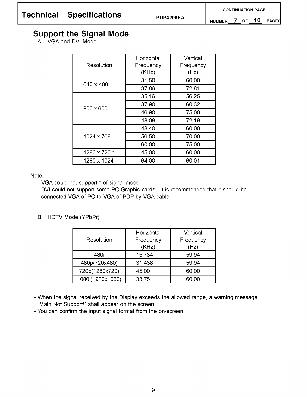
Support the Signal Mode
A. VGA and DVI Mode
PD P4206 EA
CONTINUATION PAGE
NUMBER 7 OF 10 PAGES
Resolution
640 x 480
Horizontal
Frequency
(KHz)
31.50 60.00
Vertical
Frequency
(Hz)
37.86 72.81
35.16 56.25
37.90 60.32
800 x 600
46.90 75.00
48.08 72.19
48.40 60.00
1024x 768
56.50 70.00
60.00 75.00
1280x 720 * 45.00 60.00
1280x 1024 64.00 60.01
Note:
- VGA could not support * of signal mode.
- DVI could not support some PC Graphic cards, it is recommended that it should be
connected VGA of PC to VGA of PDP by VGA cable.
B. HDTV Mode (YPbPr)
Resolution
Horizontal
Frequency
(KHz)
Vertical
Frequency
(Hz)
480i 15.734 59.94
480p(720x480) 31.468 59.94
720p(1280x720) 45.00 60.00
1080i(1920x1080) 33.75 60.00
- When the signal received by the Display exceeds the allowed range, a warning message
"Main Not Support!” shall appear on the screen.
- You can confirm the input signal format from the on-screen.
9
Page 11

Technical Specifications
Remote Control
PD P4206 EA
CONTINUATION PAGE
NUMBER 8 OF 10 PAGES
E Standby ( 0 ): Press to turn on and off.
2
Mute ( [& ): Press to mute the sound.
Press again to restore the sound.
3 0~9 Number Buttons: Press 0~9 to
select a channel, and used to input the
password; the channel changes after
2 seconds.
4 EPG: Press to display EPG mode.
Press it again to exit EPG mode.
5 Input: Press to select the signal
source, such as TV, AV, S-Video,
Component 1, Component 2, VGA,
DVI or DTV.
6 DTV: Press to choose DTV directly.
0 Dot: Press number buttons with it to
select the channels directly in DTV.
8 VOL +/-: Press to adjust the volume.
9 CH +/- : Press to select the channel
forward or backward.
10 MTS: Press repeatedly to cycle through
the Multi-channel TV sound (MTS)
options: Mono, Stereo and SAP
(Second Audio Program).
11 ◄ ,►,▲,▼, Enter: Press ◄ ,►,▲,
▼ to move the on-screen cursor. To
select an item, press Enter to confirm.
And it can also press ▲ or ▼ to
select channels, press ◄ or ► to
adjust the volume.
12 Exit: Press this button to exit.
13 Menu: Press to enter into the on-screen
setup menu, press again to exit.
14 V-Chip: Press to select the child
protect mode.
11 CCD: Press to select the Closed Caption mode.
11 Freeze: Press to freeze the picture, press again to restore the picture.
11 Display: Press to display the channel information and it disappear after 3 seconds.
11 Favorite: Press repeatedly to cycle through the favorite channel list.
11 Add/Erase: Press to add or delete favorite or dislike channels.
20 S.Mode: Press repeatedly to cycle through the sound mode: Normal, News, Cinema,
Flat and User.
21 PIC Size: Press repeatedly to cycle through the picture size that best corresponds your
viewing requirements: Normal, Full, Widel, Wide2, Wide3, 4:3, No Scale and Panoramic.
20
22
24
20
20-
Standby
rh
:(D CD CD'
.® CD ®
®
-O p Q O
® / Glx
"EPS / Tnput
o <§>
Red _ //G ree n Y e llo w \ _ B lu e
p o o o v
-2
-4
-20
-20
-22
-20
10
(Continued on next page)
Page 12

Technical Specifications
22
P.Mode: Press repeatedly to cycle
through the picture mode: Normal,
Vivid, Hi-Bright, User and Dark.
23 System: Press repeatedly to cycle
through the system options: AUTO,
and NTSC3.58.
24
Recall: Press to return to previous
channel.
22
Sleep: Press repeatedly until it
displays the time in minutes (5 Min,
10 Min, 15 Min, 30 Min, 60 Min, 90
Min, 120 Min and, OFF) that you
want the TV to remain on before
shutting off. To cancel sleep time,
press SLEEP repeatedly until sleep
OFF appears.
22
Red: Press this button to access the
red item or page.
22
Blue: Press this button to access the
blue item or page.
22
Green: Press this button to access
the green item or page.
22
Yellow: Press this button to access
the yellow item or page.
PD P4 206 EA
rn-
3
6
22
22
22
22
22-
CONTINUATION PAGE
NUMBER 9 OF 10 PAGES
Standby Mute
'CD CD
CD
CD CD/ CD/1
CD CD!
"EHS
o
CD)
- Tnput
(S>
0 D Ö Q
— ! vol ! "TS !^rt-
P.Mode Reca ll S lee p System
O O Q O
Green Y e ll o w \ _
p o o o v
-a
-7
-22
-22
-22
-22
Note: Press CH +/- on the remote control can turn on TV set from standby mode.
Insertion of Batteries:
- Turn the remote control upside down, press and slide off the battery cover.
- Insert two 1.5V (AAA) batteries into the compartment, take care to observe the © and ©
markings indicated inside.
- Replace the cover and slide in reverse until the lock snaps.
i i
Page 13

Technical Specifications
PHYSICAL CHARACTERISTICS
14. Power Cord
PD P4 206EA
CONTINUATION PAGE
NUMBER 10 OF 10 PAGE
S
Length :
Type :
15. Cabinet
15.1 Color :
15.2 Weight
Net weight
Gross weight
15.3 Dimensions(with stand)
Width
Height
Depth
1.8m nominal
optional
“Black” colour as defined by colour plaque reference number
36.2 kg(with stand) /34.0kg(without stand)
41.0 kg
1040 mm
690 mm
290 mm
12
Page 14
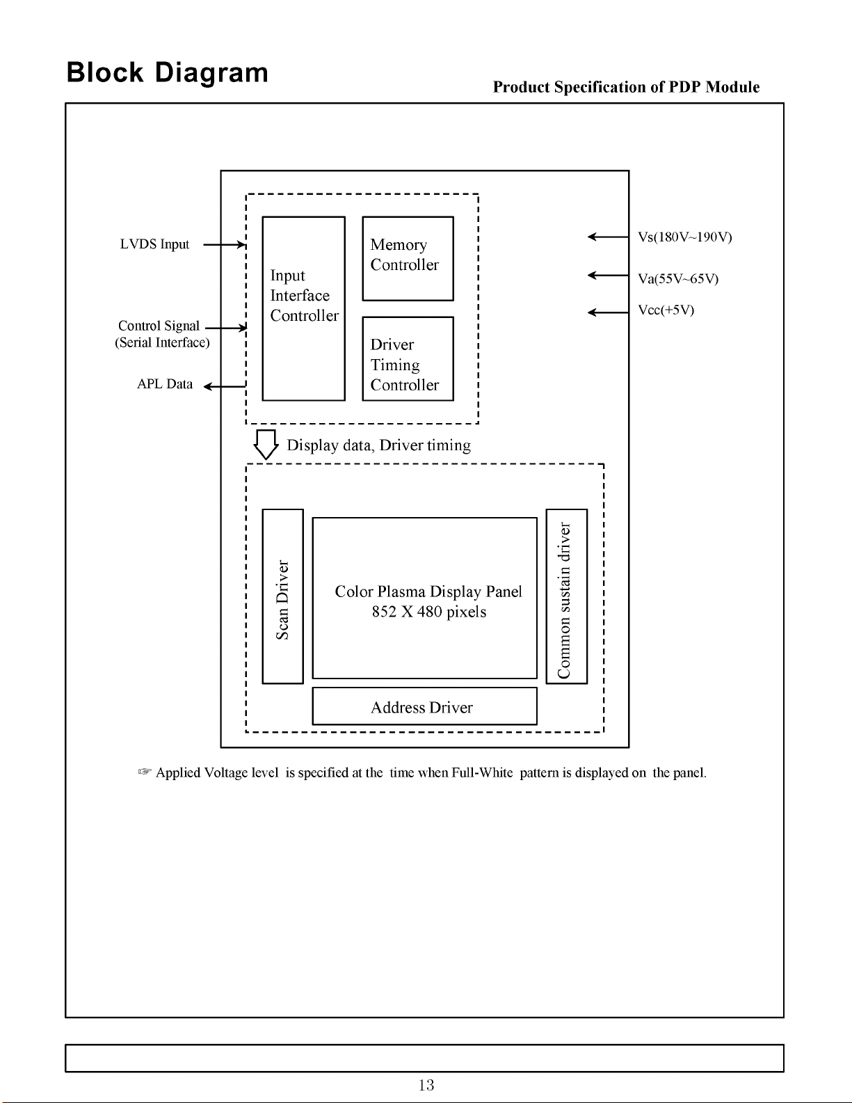
Block Diagram
Product Specification of PDP Module
LVDS Input
Control Signal —
(Serial Interface)
APL Data
Memory
Input
Interface
Controller
Display data, Driver timing
>
•c
Q
G
cd
O
GO
Controller
Driver
Timing
Controller
Color Plasma Display Panel
852 X 480 pixels
<u
>
•G
T3
cö
3
c
O
a
a
o
O
Vs(180V~190V)
Va(55V~65V)
Vcc(+5V)
Address Driver
Applied Voltage level is specified at the time when Full-White pattern is displayed on the panel.
13
Page 15

Block Diagram
14
Page 16

Block Diagram
—3.3V-
From MT3551
AV1 Audio >
AV2 Audio >
N
{
) o
— 5
K)
AV Audio in
15
Page 17
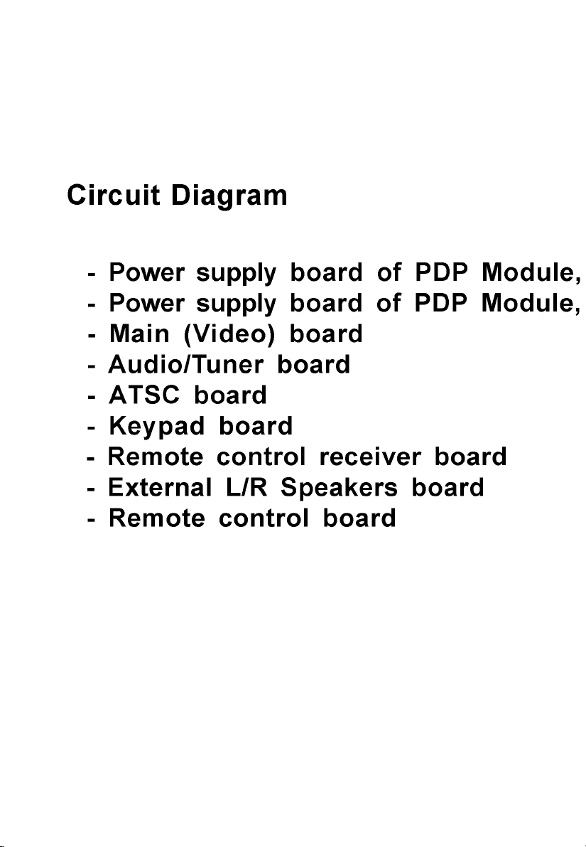
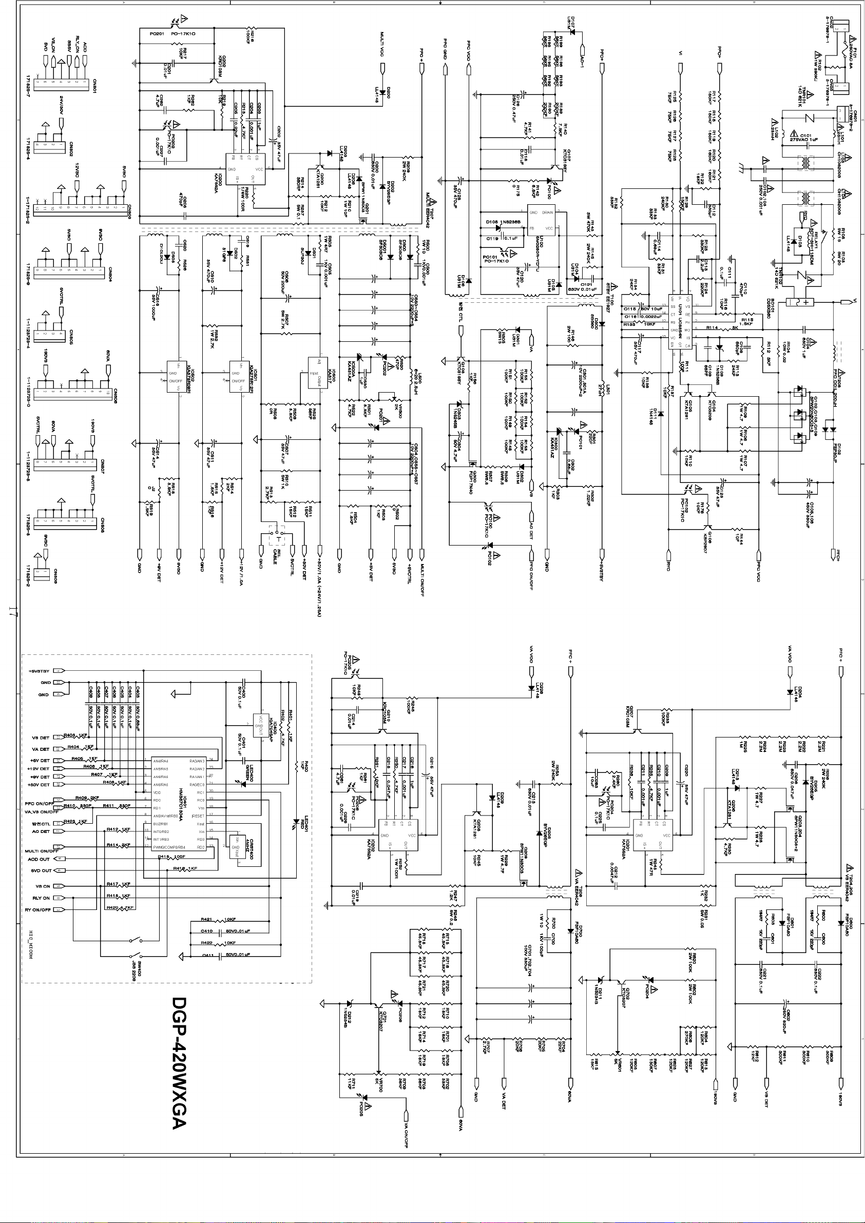
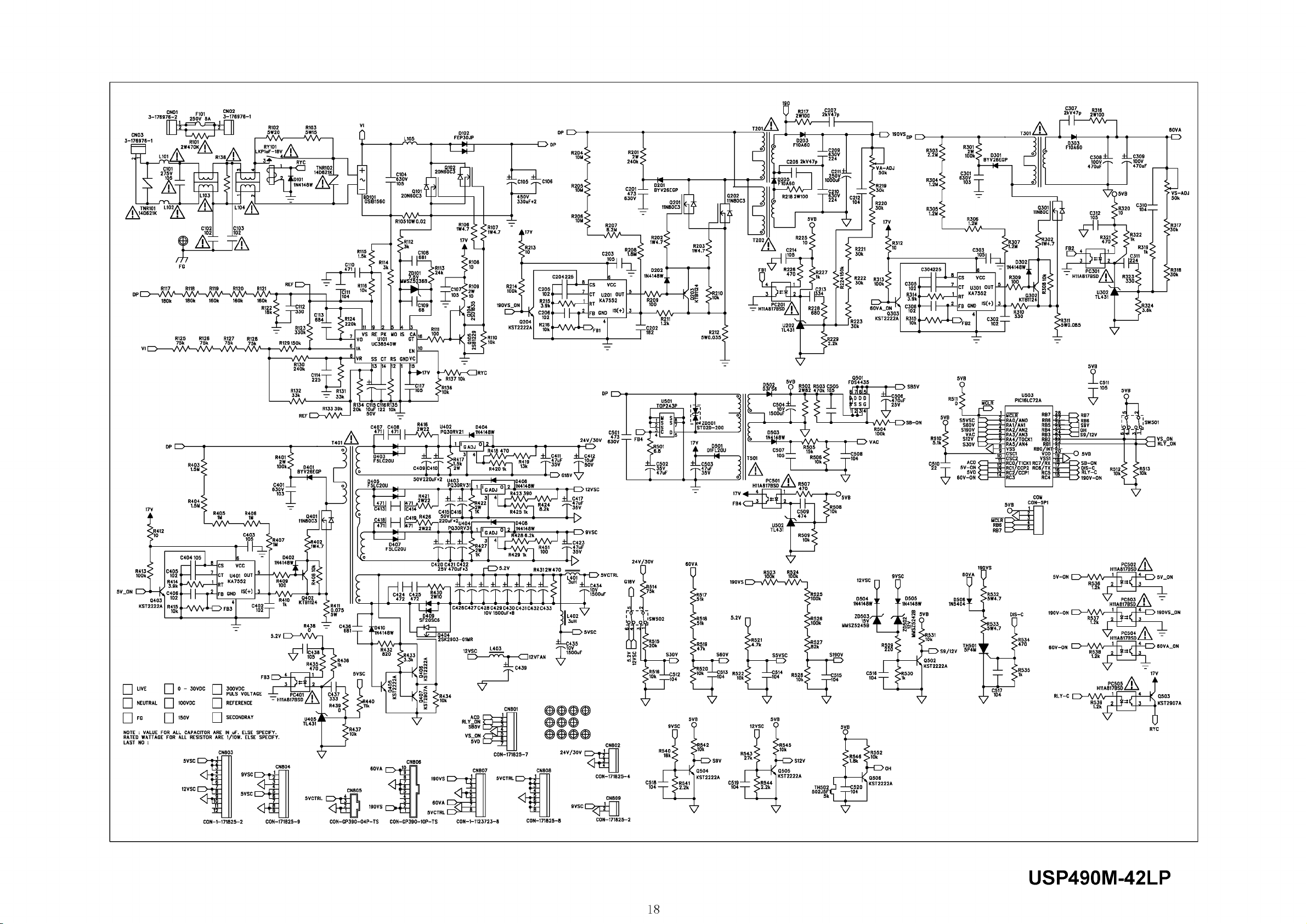
Circ ui t Diagram
- Power supply board of PDP Module,
- Power supply board of PDP Module,
- Main (Video) board
- Audio/Tuner board
- ATSC board
- Keypad board
- Remote control receiver board
- External L/R Speakers board
- Remote control board
Page 18
DGP-420WXGA
USP490M-42LP
16
Page 19
Page 20
□ LI VE
| | NEUTRAL Q 100VDC | | REFERENCE
□ rG
NOTE : VALUE FOR ALL CAPACITOR ARE IN uF. ELSE SPECIFY.
RATED WATTAGE FOR ALL RESISTOR ARE 1/10W. ELSE SPECIFY.
LAST NO :
Q 0 - 30VD 1 1 300VDC
| | 150V
1
-----
1 PULS VOLTAGE
| | SECONDRAY
CO N-171 825-9 C0 N-GP3 9Q -0 4P -T S
60V A [
5VCTRL
C0 N-GP3 90 -1 0P -T S CON -1-11 23723-8
CON—171825—8
CON-171 82 5-2
USP490M-42LP
18
Page 21

MT8205E (PBGA388) LCDTV BOARD 4 LAYERS
1. INDEX
2. LDO
3. MT8205E PBGA388
4. MT8205 ANALOG DECOUPLING
5. DDR MEMORY & FLASH
6. VGA IN & PC AUDIO IN
7. VIDEO IN & TUNER IO
8. AUDIO/VIDEO IN CIRCUIT
9. DVI INPUT
10.LVDS/CRT/TTL OUT
11.BACK LIGHT / KEYPAD
12.WM8776 & A/V BYPASS
13.ATSC INTERFACE
14.PDP INTERFACE
5VSE
SYS TEM EEPROM
U2
0.1uF
EEPRO M 24C16
SOPE/SMD
GN D SDA
O UVU'
5VSt
R337 R3
+ CE 1
“ 220uF/16v
C220UF16V/D6H 11
DV1EA
Power down Reset circuit
R73 . . .10/NC
W 10/N C,
DV33A R34
W 10 •
47uF/16v
D2E
1N4148
RSRXD
RSTXD PCTXD
C1 0.1uF
5VSB
C2 0.1uF
C3 0.1uF
C5 0.1uF
SYS P WR J4
OUSING
PH5/2.0
U1
R2IN
T1IN
T2IN
MAX232A
^ R2
^ 1 W
3 :SOT23/SMD 4.7k
1 2N3904
R1OUT
R2OUT
T1OUT
T2OUT
2N3904
VCC
GNL
►>RSRXC
►>RSTXC
&P CR XC
>>PCTXC
+ 12V
►>TUNER_12V 7
►>E205UP3_1 3
>SP WR_ GND 11
►>INVERTER_PWR 11
►>GPIO_DVD1 3
AD D BY MTK
PCRX D
5VSB DV33A
* R336
0
16
15
ADD BY MTK
E205UP3_1 HIGH :POWER OFF
E205UP3_1 LOW :POWER ON
E205UP3_1
NVERTER_PWR
I INV ERTER PWR
PW R_ GN D
J3
D
►>DV1EA 2,3
RS-232
I M11 9 M 21 9 M3
I V11 # V 21 # V 31 $ V4
L44 l5I_
FE
BEAD/SMD/120
AUIO IN/OUT GND ANALOG INPUT GND
-E
EEAD/SMD/1206
DIGITAL GND
19
VCC
For Tuner
_•
+12V
+ CE2
-v 220uF/16v
C220UF16V/D6H11
_ O A _
BEAD/SMD/0E05
T
TUNE R 12V
ize I Doc Number
C INDEX
Wednesday, October 12, 2005
V1.2
J2
Page 22

J/NC
Power ON alive source
— » DV 1 8A 1,3
20
:e Doc Number
c LDO V1.2
Date: Wednesday, October 12, 2005 I Sheet 2
Page 23

ADCPLLVDD1
ADCP LLVD D
>>XTALI •
»XT ALO •
A
a na lo g v d d •
»A DC VD D •
»AP LL VD D •
»VP LL VD D •
»ADCPL LVDD1 •
»A DC PL LVD D •
ÄAU XT OP •
ÖAU XB OT TOM •
>> REXTA •
»A PLL ^A P <
>Sp wm2vref •
»A DCV DD O •
»A DCV DD 4 •
»A V C M •
ÄV O C M •
>>VICM •
ÄV RE FP4 •
»V RE FN 4 •
>>DACFS •
&D AC VR E F •
>>DACVDD •
>Slvd d a •
>>IR
JV18A
GND
CBC7
U/
^ ^ 3 > > > > > > 3 c i D ' o
VFEVGG1
51
ADCV DD4
SIF
AF
ADCVSS 4
REFP4
REFN4
ADCVSS
ADIN4
AGINS
ADIN2
ADIN'
ADINO
ADC VDD
PWM 2VR EF
AUXVTCf
AUXV BOTT OM
VPLLVSS
VPLLVDD
DLLVDD
DLLVSS
BGVSS
REXTA
BGVD D
LVDDA
A7P
A7N
CLK2P
CLK2N
LVSSA
AEP
AEN
A5P
A5N
LVDDB
A4P
ASP
ASN
LVSSB
CLK1P
CLK1N
A2P
A2N
LVDD C
A'P
AOP
AON
LVSSC
DAC VD DC
VREF
FS
DACVSSC
SVM
DAC VDD B
DACV SSB
DACVDDA
G
DACV SSA
B
R
DE
VSYNCO
HSY NCO
VCLK
EBO7
EBOE
EBO5
EBO4
GVGGS
EBOS
EBO2
EBO'
EBOO
EGO7
DVSS'£
EGOE
AA1
EGO5
AA2
EGO4
AAS
EGOS
AA4
EGO2
AB1
EGO'
AB2
EGOO
ABS
ERO7
AB4
EROE
ERO5
.A.C1
GVGG1£
AC 2
ERO4
EROS
ERO2
GVSSS
ERO'
EROO
OBO7
OBOE
OBO5
SYP
SYN
VO CM
REFP'
REFN'
VFEVSSO
ADCVSS'
VFEVDDO
DV88A DV18A
DV88A DV18A
Page 24

r
TI
r
" L
_r
" L
DV18A
ADCPLLV DD1
VICM
— DV18A
>>DA CVRE F 3
»D A CF S 3
»AD CPL LV DD1 3
»A DC PL LV DD 3
»AP LL VD D 3
»A NA LO G VD D 3
»VP LL VD D 3
>>LVDDA 3
»VR EF P4
>>VREFN4
»A DC VDD C
»A DC VDD 4
ÄP WM 2VR EF
ÄAU XTO F
»AU XBO TTO M
>S REXTA
>>APLL_CAP
»XTALI
>>XTALC
1 .2.3
MT8205 ANALOG DECOUPLING&DIGITAL DECOUPLING
CE22 C 1uF
47uF/16v | C0603/SMD
ADCPLLVDD1
CB42
L7
_ n r \ _
BEAD/SMD/0603
I
R20
1
**T'* 22uF/25v CC6C3/SMD
1
.«'T'' 47uF/16v CC6C3/SMD
R22
1
**T'* 22uF/25v CC6C3/SMD
CC6C
----------
I C^ X
1 + CE14 = 4.7uF =
----------
I C T T
1+ CE15 ^ ^ 4.7uF
----------
I C H T
1+ CE2C = 4.7uF =
— ,_4 .7uF —
C0603/SMD
GND
ADCP LLVD D
GND
ANALOG VDD
GND
GND
ANA LOG VDD
VREFP4 ADC _VD D
XTAL
R19
Hül-
Y1 27MHz
C11
33pF
L1C
BEAD/SMD/0805
L13
BEAD/SMD/0603
CB24
X
0.1 uF
C0603/SMD
T .
I CB28
T ° 1uF T
CB33
T ° 1uF T
47uF — I—
C0603/SMD
T
DAC VREF C33 II 0.1uF/NC GN D
APLL CAP C 32 II 1500pF G N D
REXTA R2 4. . .3.3k
DACFS R27 . . . 560 GND
______
R23
0
L11
DV18A
DIGITAL DECOUPLING
CB25 CB26 CB31 C22
0.1uF 0.1uF 0.1uF 0.01uF
=^= CB37 = ; = CB38 = ;= CB39 I^= CB40
0.1uF 0.1uF 0.1uF 0.1uF
C0603/SMD C0603/SMD C0603/SMD C0603/
R21
0
BEAD/SMD/0603
- J W .
BEAD/SMD/0603
_9
+ CE21
47uF/16v
CE19
I C19 I CB27
Z = 4.7uF = 1 0.1uF
C0603/SMD C0603/S
I C21 I CB29
^ ± 4.7uF 0.1uF
C0603/SMD C0603/S
— ,— 47uF — ,—
C0603/SMD
T
" L
0.1uF
C0603/SMD
_______
GND
GND
0603 PUT ON NEARLY BGA
r . C29
3300pF 3300pF
C0603/SMD C0603/SMD
GN D
0603 PUT ON NEARLY BGA
T
I .
SMD
T
" L
1 “
X
GND
GND
50/47R AUXTOP
50/47R A UXBOTTOM
TP5
TP6
22
ize Doc Number
C MT8205 DECOUFOMG--ANALOG
Wednesday. October 12, 2005
V1.2
Page 25

A DQSÍQ..31 xx A_DQS[Q..3] 3
111' « A_ RA[Q..11] 3
T n « A_BA[Q..1 ] 3
TQ ^ r A_DQM[Q..1 ] 3
A_DQ[Q .31] 3
A_CKE
A_CS#
A_RAS#
A_CAS#
A_WE #
SDV25
VREF
PWR#
PCE#
F_OE#
F_D[Q..7]
F_A[Q..2Q]
D RA1 '
D_RA1Q R32
RN2
RN4
RN
RN
---1 V S / S A
RN3 22x4
--
1
RN5 22x4
RA11 D RA 1' 75x4
22x4
A_RA1 QR31 22 D_RA1Q
RN7 75x4
--
1
RN9 47x4
75x4
6
8
MX29LV16QBI
TSOP 48 p i n
RN1Q 47x4
— 7
RN12 47x4
47x4
RN16 47x4
18 47x4
RN2Q 47x4
DQ28 7
A DQS Q R 33.
A DQS1 R34 .
A DQS2 R35 .
A DQS3 R36 -
A_BA1 R D_BA1
A_BAQ R4Q D_BAQ
A DQMQ R 43-
A DQM1 R 45.
A_CKE D_CKE
A_CLK D_CLK
A CLK# R51 .
8
D_DQ 28 75x4
47x4
47 D _DQSQ
47 D_DQS1
47 D_DQS2
47 D_DQS3
RN24
22x4
D_DQ MQ
D_DQM1
D_CLK#
75x4
CB52 CB53 CB54 CB55 CB56 CB57 CB58 CB5
Q.1uF Q.1uF Q.1uF Q.1uF Q.1uF Q.1uF Q.1uF Q.1u
75x4
75x4
75x4
75x4
22QuF/16v
75x4
75x4
RN23
D_RAS#
7
75x4
D DQ S2 R3 7.
D DQ S3 R3 9.
TP7
D_CAS# R42
D_DQM1 R46
D_DQS1 R48
D_DQ SQ R5Q
D_DQMQ R52
CB6Q CB61 CB62 CB63 CB64 CB65 C B66 CB
Q.1uF Q.1uF Q.1uF Q.1uF Q.1uF Q.1uF Q.1uF Q.1u
,
D W 2 5
.................................................................
rDRo Í-DRO CB7Q CB71 CB72 CB73 CB74 CB75 :
j DBuF y D.1uF Q.1uF j D.1uF | D.1uF DBuF DBuF Q.1ui
_
« n r n r n r n r n r n r n
+CE24
---
33QQpF C35 C36 C37 C38 C39 C4Q
| 33QQpF 33QQpF 33QQpF 33QQpF 33QQpF 33QQpF
---
C B8Q CB81 CB82 CB83 CB84 CB85 CB
Q.1uF Q.1uF Q.1uF Q.1uF Q.1uF Q.1uF Q.1uF
~ “ CB88 CB89 CB9Q
Q.1uF Q.1uF Q.1uF Q.1uF Q.1uF Q.1uF
T
---
C42 C43 C44 C45 C46 C47 C48
33QQpF 33QQpF 33QQpF 33QQpF 33QQpF 33QQpF 33QQpF
CB91 CB92 CB93
..........
86
CB94
Q.1uF
a
67
----------
~ T" Q.1uF I Q.1uF I Q.1uF I Q.1uF
_ V RE F
Í
VREF DECOUPLING
I
| CB11Q | CB111 | CB112 | CB113
j Q.1uF I Q.1uF I Q.1uF | Q.1uF
CB1Q9
-----1--------1--------1--------1------
Q.1uF
Q.1uF
VCC
+ CE31
L16
_ r v ^ _
BEAD/SMD/Q8Q5
22QuF/16v
U 1 3 CM1117-2.5V
IN OU
SOT223/SMD
T
2
CE27
22QuF/16v
1+ CE29 1 +CE28 1+ CE29
22QuF/16v X " 22QuF/16v '
23
+ CE3Q
22QuF/16v
T
~ j~ Q.1uF j D.1uF j D.1uF j DBuF D.1uF Q.1uF | D.1uQ | I
:e Doc Number
C DDR MEMORY&FLASH
esdav. October 12, 2QQ5
V1.2
Page 26

A
B
C
D
E
VGA_PLUGPWR
VGA PLUGPWR
CB115
L17
FB
BEAD/SMD/0603 ? R61
L18
FB
BEAD/SMD/0603 R62
U14
NC
NC
NC
GND
EEPROM 24C02
> 2.2k “ C50
> 2.2k ^
VCC
WP
SCL
SDA
0.1uF
M o d ifie d by
¡H C51
5pF
GND
VGAVSYNC #
Bin _ w a n g .22/7 /0 5
HSYNC VGA
R53
R54
10k
10k
Title
Doc N um ber
Size
B
A B C D E
Date: W ednesday, October 12, 2005
VGA IN&PC A U D IO I
I Sheet ~6~
24
Rev
V1.2
Page 27

Page 28

Page 29

DVIDE
DVIH SYNC
DVIVSY NC
DVI_P LUGP WR
0.1uF
DVI_PLUGP WR
GND SDA
EEPRO M 24C02
DVIPWR
- S -
C104 C105 C106 C107 C 108 “
| 220pF 10uF/10v | 220pF 10uF/10v | 220pF |
DVIP WR
FB BEAD/SMD/0603
DVIP WR DVIPVCC
FB BEAD/SMD/0603
DVIP WR
S-
FB
L32
---
L33
= .
I :
DVI_ PLUGP WR
DDCD VISCL
DDCD VISD A
DVI_P LUGP WR
DVIP WR
CE45
100uF/16v
_ CB118_
C95 U p
1 0uF/1 0v 0.
CB117
0.1uF
DVIP WR
DVIPWR
3-
EXT_RST
AD D BY MTK
DVIP WR
-8.
---
C110 C111 C112 C113 C100 C101 C102
220pF 10uF/10v 220pF 10uF/10v 220pF 10uF/10v 220pF
DVIPWR
DVIP WR
DVIP WR
DVIP WR DVIP WR
DVIP WR
-0.
CLOCK+ DDC _SC L DDC _SD A
SOT23/SMD SOT23/SMD SOT23/SMD
OGN D
QO23
O
VCC
AGN D
RX2+
RX2-
AVCC
AGN D
AVCC
AGN D
AVCC
AGN D
RX0+
RX0-
AGN D
RXC+
RXC-
AVCC
DVIPVCC
EXT_RST
PVCC
PGND
RESER VED
OCK_INV
DVIPWR
S-
VCC
_C
ooooooo^yooooooc
ooooooooooooo
Sil 161B
Sil 169
TQFP100/SMD
PQQQQ QQQQ OOOQQ QQQ
U18
VCC
_C
DVIPWR
Jt-
.jO OO O OC
¡.oooooc
HSYNC
VSYNC
OGN D
ODCK
OVCC
OVC C
OGN D
CTL3
CTL2
CTL1
QE23
QE22
QE21
QE20
QE19
QE18
QE15
QE14
QOC
GND
VCC
DE
D31
SOT23/SMD
VCC
_C
DDCD VISCL
Add By MTK
DVIODCK0
DVI-I DIP 34P
□□□
□□□
□□□
c_SCC6
VCC
_S
VCC
_9
DVIH SYNC
□□□
□□□
□□□
□□□
□□□
RED
GREEN
WHEN USE Sil169//Sil161 ADD R175 , NC R345
WHEN USE Sil1169 ADD R345,NC R175
BLUE
'6^ 10
VCC
_C
DATA0+ DATA1+ DATA2+
DV H SYN C0
■ RN25^
VCC
_C
VCC
JC
DVIPWR
R1
> R/[
Add by MTK
D18
DVI_PLUGPWR
Add By MTK
-
DVIP WR
R344
R/NC
> R345
> 10k/NC
R175
>
0
SOT23/SMD
VCC
SOT23/SMD
VCC
VCC
1N4148/SMD
DDCD VISCL
DDCD VISDA
R322 R323
0/NC
"LIT----------
---1 M OSF ET N 2N 7002
DV33A SOT23/SMD
---1 MOS FE
DV33A
DV33A SOT23
L J
R91
^ —
0/NC
R0603/SMD
WHEN USE Sil169/sil 1169 ADD
DVIPWR
F_A21 R330
330^
When use Sil169//Sil1169 R172 NC,Add R326
WHhen use Sil161 R326 NC,Add R172
DVIPWR
R346
M S#
When Sil 169/Sil161 R346 NC
Add R347
10k/NC
R347
10k/NC
27
R174
10k/NC
DVISCL REPLACE OCK_INV NET
DVISDA REPLACE ST
WHEN SIL161 ADD R173 R174
WHEN Sil169/ Sil1169 R173 R174 NC
DVIPW R DV IPWR DVIPWR
R327 R328
4.7K/NC > 4.7K/NC
OCK
WHEN USE Sil1169 add R331 R332
WHEN USE Sil169 add R327 R332
WHEN USE Sil161 NC R331 R332
:e Doc Number
C DVI INPUT
Date: Wednesday October 12 2005
hen use Sil169/Sil 1161 ADD R333
W
R329
4k7/N C
'
Page 30

>>SDA
►SoRoe
>>GPIC
ORO5
8205UP1 4
7,13
3,/
WHEN USE Fujitsu 4 2 PDP ,ADD R179 R186 R187 R185 R286 R291 R293.REMOVE R178 R290 R292
LVDS OUT(Include PDP and 32' LCD LVDS interface)
WHEN NOT USE PDP ADD L49 R178 R290 R292
REMOVE R179 R185 R186 R187 R291 R293
4.7K REPALAC 47K
28
CRT O UT.
ize I Doc Number
C LVDS/CRT OUT
Wednesday, October 12, 2005
V12
of
Page 31

OBOI0
0B0|0..7| 3
>>IR 3,7
>Sp w r _g n d 1
>>INVERTE R_PWR 1
OBO' + CE50
PW R_ G ND
OBOC
OBO1
o b o ;
OBO3
OBO4
OBO5
OBOE
OBO7
8205UP3_0
PWM 0 3,14
►>8205UP1_2 3,9
— » PW R_GND 1
VCC
nverter_PWR
470uF/50v
PANEL INVERTER POWER
:E51 CB121 CB122
70uF/50v 0.1 uF 0.1uF
PW R_ GND
FOR AU 32" INVERTER CONNECTOR
29
Size Doc Number
C BACK_LIGHT/KEYPAD
Date: Wednesday October 1 2 2005 IShee~
of
Page 32

COD HP OU TR C125
COD H PO UTL C
r
5VSB
MUST USE SHIELD CABLE
1 2 S t
TO AUDIO BD
-V
CONt
A / V B y p a s s
VCC
R233
0
R0805/SMD
AUDIO BYPASS.
_ AO SDATA 3 R234 .
DAC MC LK R237 ,
BEAD/SMD/0805
VCC
SDATA A OUTL
DEM#/SCLK VA
LRCK AGN D
MCL K AOUTR
DIO DAC
l BYPASS
R BYPASS
i
VCC
I
Size Doc Number |R e
C WM8776/WM8766/AUDIO CODEC
30
Date: Wednesday, October 12, 2005 Sheet 12 of
Page 33

+12V
+12V 1,7,10,14
8205U P1_3
REQUEST#
VI[0. .23]
5VSB
DVIVSYNC
DVIHSYNC
DVIDE
DVIO DC K
8205U P1_3
RE AD Y# 3
REQ UEST# 3
_ OGO 4 3,«
>>OGO5 3
>>OGO6 3,7
^ V I[0 ..23] 3,9
&O GO3 3
>>OGO1
>>OGO2
>>OGO0
>>SW
DV33A
R252
10k/N C
VCC
5V
3,12
+12V
LO = > DTV BOARD POWER ON
HI = > DTV BOAR D POWER OFF
DV33A 5VSB
DV33A
I
------- Q9
0
2N3904
DV33A
o
DV33A
5VSB
R248
R249
10k
10k/N C
SW
R251
0
MTK Modify
5VSB DV33A
, L46 f L47
fb/nc C fb
2N3904 J
SOT23/SMD
Q10 1
R247
R250
—/S / S / N—
0/NC
10k
DV33A
C135
56pF
—20 VCC
— 10 GND
74LV C244A
U31 74LVC244A
VCC 2G 19
U32 74LVC244A
2G 19
1G O 1
74LV C244A
17
15
■GND Need Very Strong"
OGO4
Trace width of 12V>30mil
T race width of 5V >40mil
5V
TXD 0:MT5351 Transm it
ry d - 0 ' M T 5 3 5 1 Receiver
TX D 2:M T5351& MT8205 Com m unic ation
R< D _2:MT5 351 & MT8205 Com mun ication
DIP 8/W /H /P2.54
WE#
U29
74LV C00A/N C
A
ja
JP3/DIP/P2.54
PCTXD
a
13
RXD 0
PCRXD
10
TXD 0 —
r
DV33A
DV33A
R255
10k
8205UP1 3 46
WHEN OGO4 HIGH , DVI OUPUT
SW
0
1
Function
PC < ...> MT5351 U0
MT5351 U2 <---> MT8205
PC <---> MT8205
P C
-----
> MT5351 U0RX
2N3904 ‘
SOT23/SMD
Q11 1
0/NC
REQUEST0#
WHEN OGO4 LOW ,ATSC OUPUT
ADD 22/9
Title
Size Doc Num ber
Cus om ATSC INTERFACE
Date: We dnesd ay, O ctobe r 12, 2005 I Sheet
13 o f
Re v
V1.2
"3T
Page 34

A
4 4
+12V
ORO1
ORO3
PWM0
ADIN4
ADIN4
3 3
>+12V
>ORO1
>O'O 3
>PWM0
>ADIN4
<§) TP3
1,7,10,13
3.10
3.10
3.11
3
B
CN2
1
“ ^ E L A Y ON
2
5VSB
3
GND
4
VS ON
5
5VD
6
7
[
DIP7/P2.0
DEL ACD Net-
-MTK
C D E
Change- -MTK
2 2
VCC
Q
+ CE80
-v 220uF/16v -
C220UF16V/D6H11
A B C D E
+12V
Q
+ CE79
220uF/16v
C220UF16V/D6H11
Title
SizeADoc Number
Date: Wednesday, October 12, 2005
USE WHEN LG V6
USE WHEN LG V6
PDP interface
Sheet 14 of
I
Rev
V1.2
15
Page 35

A B C D E
From V0.1 To V1.2 change item:
4 4
1,Add R109-10K;R107-4.7K;C135-56pF;0603-R88,R91,R104,R106-0^M.0805-R96,R99,R101-0^^
2,Reset IC ^ # P 5 V Supply;DVI AUDIO ADD CONNECTOR J8.
3,ADIN4 CHANGE TO PWM0
3 3
2 2
Title
SizeADoc Number
History
Rev
V1.2
Date: Wednesday, October 12, 2005 | Sheet 15 of 15
A B C D E
Page 36

Page 37

MT5351RA-V2
A
MT5111 / MT5351 REFERENCE DESIGN - 4 LAYERS
Rev History P# DATE
RA-V1 INITIAL VERSION 2005/06/15
RA-V2 ADDE D AUD IO SW ITCH / REFINE POWER C IR CUIT 2005/07/14
01. INDEX AND INTERFACE
02. POWER
03. TUNER
04. MT5111 ASIC
05. MT5351 ASIC
06. MT5351 PERIPHERAL
07. DDR MEMORY
08. NOR FLASH / JTAG / UART
NAME TYPE DEVICE
+12V POWER +12V POWER SUPPLY
+5V POWER +5V
+5V tuner POWER +5V
DV33 DM POWER +3V3 MT5111 POWER
DV18 POWER +1V8
DV33 POWER +3V3 MT5351 POWER
AV33 POWER +3V3
DV25 POWER +2V5 MT5351 DDR POWER
DV12 POWER +1V2
POWER SUPPLY
TUNER POWER
MT5111 POWER
MT5351 ANALOG POWER
MT5351 POWER
NS : NON-STUFF
BEAD/SMD/1206
J-
DIP8/W /H/P2.54
_ L1 ^ FB
- ± CET
,*-T>,22ÜuF
C220L
CE2
' 20uF/16v
C220UF16V/D6H11
+3.3V
POWER INPUT FROM MAIN BOARD
DV33
C
C0603/SMD
2.5.6.'8 DV33
5,6,7,18 GND
5,8 ORESET#
5 REQUEST#
5 READY#
GLO BAL SIGNA L
5 ASPDIF
5.8 U0RX
5.8 U0TX
5.8 U2TX
5.8 U2RX
UART (R S232)
|5 VO R[0..7]
5 VO G[0..7]
5 VOB[0..7]
5 VOPCLK
5.8 VOHSYNC
5.8 VOVSYNC
5 VODE
DIGITA L VIDEO OUTP UT
5 AO1MCLK
5 AO1LRCK
5 AO1BCK
5 AO1SDATA0
5 ASPDIF
DIG ITAL A UDIO IN TER FAC E
5 AUD_CTRL
«»-
«»-
«»-
«»-
" VOPCLK“
AO1SDATA0
GND GROUND GROUND
9 FB1
I
__
BEAD/SMD/0603
SPDIF CIRCUIT
DIGITAL OUTPUT
Title POWER
Size Document N
IDate:
35
Page 38

36
Page 39

C
D
t
2,14 +5V_TUNER « » •
1,2,4,5,6,7,j8 GND
: _ « » .
+5V TUNER
GND
GLO BAL SIGNAL
4 RF_AGC
4 IF_AGC
4 2nd_IF+
4 2nd_IF-
4 TUNER_SCLO
4 TUNER_SDAO
RF_AGC
F_AGC
2nd IF+
TUNER SCLO
TUNER SDAO
TUNER INTERFACE
Title
TUNER
Document Number
Size
,m MT5351R A-V2
Cust
C
D
Date: Monday, September 26, 2005 Sheet 3 of 8
Rev
1
TwinSon Chan
37
Page 40

38
Page 41

Ü^È
"•iE Hdü=
1,2,3,4,6,7,b GND « » GND
^ S S S T I I e H YeE E :
6 O1DA0
6 opwm0
6 OXTALI
6 WXUJ Vk //
GLOBAL SIGNAL
Tm îN î"7]
TS
7 s f
7 = '
ÏP25R27? g
FLASH INTERFACE
1 AO1MCLK <<
1 A O i L 1
AUDIO INTERFACE
ï u a
JTAG PORT
n n
L UART (RS 232)
______
---
39
ANALOG PART
€ Lm„ ^ Lm^ Lm.
Add by Ada
Page 42

CAPVP
_ C2
0
C0
Î
C101
h
■ 0uF/10v
C0805/SMD1
C
f-
C3
= 10
C0
DV12 FB7
BEAD/SMD/0603
MEM VREF
FS
R37
NS/560
R0603/SMD
C2
— 150
CAP VGN D
1
--------1--------
CB44 CB45 CB46 I CB47 CB48 CB49 | CB50 CB51 CB52 CB53 (
^ ^ 4 7uF ^ ^ 0 1uF ^ ^ 0 1uF ^ p 4 7uF = p 0 1uF ^ p 0 1uF ^ ^ 4 7uF ^ ^ 0 1uF ^ p 0 1uF —*— 0 1 uF — *— 0
I C0603/SMD C0603/SMD C0603/SMD C0603/SMD C0603/SMD C0603/SMD C0603/SMD C0603/SMD C0603/SMD C0603/SMD C
LEFT SIDE TOP SIDE
I C138 __I_C 140 I I CB57 _ l_ C183 _l _C184 | C185 | C 1
^ ^ 4 . 7uF ^ = 0 . 1uF ^ 4 . 7uF ^ ^ 0 . 1uF ^ ^ 0 . 1 uF ^ ^ 0 1uF ^ ^ 0
I C0603/SMD C0603/SMD C0603/SMD C0603/SMD C0603/SMD C0603/SMD CC
LEFT SIDE
"1
--------1--------
CB65 CB66 CB67 | CB68 CB69 CB70 I CB71 CB72 CB73 I CB74 CB75 CB76
^ p 0.1uF ^ p0. 1uF ^ p 0.1uF . ^ p 0.1uF ^ p 0.1uF ^ p 0.)uF . ^p0 .1uF ^ p 0.1uF ^ p 0-1uF . ^ p 0.1uF ^ p 0.1uF ^p0.1 uF
I C0603/SMD C0603/SMD C0603/SMD C0603/SMD C0603/SMD C0603/SMD C0603/SMD C0603/SMD c 0603/SMD C0603/SMD C0603/SMD C0603/SMD
LEFT SIDE TOP SIDE
I CB78 I CiCCB79
T 1 1 T
I ' ' 1
4 7uf î '0.1uF
C0603/SMD C0603/SMD
I C129 H C1
C129
_ ^ 1uF 0
0.1uF ZZ^ 0.1uF
C0603/SMD C0603/SMD
I C0i
--------1--------
--------î--------
RIGHT SIDE BOTTOM SIDE
T 1 1 T
BOTTOM SIDE
I 1 ' T
C2
--------1--------P-----
--------T--------
AVDD BGK P
AVD D DMPLL0
• R40
NS/50
R0603/SMD
ATP1 ATP2
1 --------- 1
Î c 104 H C1
:0.1uF ^ m LF
MD C0603/SMD
T 1 1 T
--------î--------- 1 1
CB80
0.1uF
C0603/SMD
CB82
" X e
_ = 0.1uF
C0603/SMD
CB85
I
0 1
0.1uF
C0
C0603/SMD
PLL0
X
MPLL1
CB87
I Cl
_ p 0.1uF
C0603/SMD
NS/10M
R0603/SMD
OXTALI
-< l>
SMD C26 C27 C 2
^ = 10nF ^ ^ 1nF ^ ^ 47
I C 0603/SMD C0603/SMD I C0
DV
33
> R45
R46
v 4.7K <
' 4.7K
R0603/SMD
R0603/SMD
OSDA0
OSCL0
C0603/SMD
R47 OSDA_MST
^ N ü0
R0603/SMD
R48 OSCL_MST
v 100
R0603/SMD
EEPROM 24C16
SOP8/SMD/NC
MT5351 SYSTEM EEPROM
DV33
V
T CB42
n b 01uF 1
1 C0603/SMD
4
VCC OUT
NC GND
OSC1
NS/74.25MHz
OSC/SMD/A
OIRI 1
2
P1
JP2/DIP/P2.54
~ NS9
•V ' NS^10
R0603/SMD
1,2 +5V
,5,8 DV33
2.5 AV33
,5,7 DV25
2.5 DV12
,7,8 GND
5 OSDA0
5 OSCL0
4 OSDA_MST
4 OSCL_MST
GLO BA L SIGN AL
5 FS
5 DVDDKP
2.5 AVDDBG KP
2.5 AVDDYKP
2)5 AVDDRKP
2.5 AVDD_DMPLL0
2)5 AVDD_DMPLL1
2.5 AVDD_VPLL
2.5 AVDD_APLL1
2.5 AVDD_APLL0
5 CAPVPLL
5 CAPV GND
5 APLLCAP1
5 APLLCAP0
5AÎ P2 $ 1
I ANA LOG PART
5 OPW M0
5 VCX00
5 U2CTS
5 OIR
« »
11
« »
B
O
«»-
«»-
«»
«»-
«»-
«»-
FS
MEM_V REF
RVREF
0PW M0
VCXO0
OIR
AVD D APLL1
AVD D APLL0
— C 1
_ = 0.1uF
1 “
— C
— p 0.1uF
CB89
C0603/SMD
CB90
C0603/SMD
40
Title
MT5 351 PER IP H E R AL
Size
m IW^T5i>51IRA-V2
Cust
Date: Monday Seotember 26 2005 Sheet 6 of 8
TwinSon Chan
Rev
1
Page 43

i 22x4 MEM WE#
MEM ADDR2
MEM ADDR8
RA12 R63 . . 22 MEM ADDR12
l/VV
65 . .
— < A A/ —
> 22x4 MEM_RAS#
RA7
22 MEM_ADDR7
22 MEM_ADDR11
CLO SED T O MT5351
MEM_ADDR5
MEM_ADDR12 R64
MEM CAS# R66
MEM ADDR3 R68
MEM ADDR11 R72 -
MEM CLKEN R78 . . NS/75
CLO SED TO DDR
+1V25 DDR +1V25 DDR
RDQ2
RDQ15
J 47x4 MEM_DQ0
R55'~ '
RN24 8
j 47x4 MEM_DQ
7 RN28 8 47x4
MEM_DQM0
1 ,2,3,4,5,6,8 GNC
5 RDQ[0..31'
5 RDQS[0..3'
5 RDQM[0..3'
5 RA[0..13]
5 RBA[0..1'
5 RCLK0
5 RCLK0#
5 RCS#
5 RRAS#
5 RCAS#
5 RWE#
5 RCKE
5 RCLK1
5 RCLK1#
6 MEM_VREF
GLOBAL SIGNA L
DDR MEM OR Y
UA L LINE LENGTH
« » DV25
—GND
MEM VREF
R7102/V
R7105^
R7106/V
4R7108A,
CLO SED T O MT5351 CLO SED T O DDR
I C168 I C169 CB95 ^ 7 ^ C y
I C0603/SMD C0603/SMD C0603/SMD C0603/SMD C0603/
C
+1V2'
C146
I C147 I C148 I C150 | C151 | C160 I 016^ | C162 | 0^63 | C^S^.
::.1uF
C0603/SMD
MD C0603/SMD C0603/SMD C0603/SMD C0603/SMD C0603/SMD C0603/SMD C0603/SMD C0603/SMD C0603,
Í
CB133 C167
0.1uF ^ 0.1uF
C0603/SMD C0603/SMD
-
BYPASS CAP. FOR TERMINATOR
(EV ERY 2 R ESISTOR PUT 1 BYP AS S CAP.)
C180 C181
0.1uF = = 0.1uF
C0603/SMD C0603/SMD C0603/SMD C0603/SMD
CLOSE D TO MT5351 CLOS ED TO DD R
41 • C142 • C143 • C144 | C145
603/SMD C0603/SMD C0603/SMD C0603/SMD C0603/S
C0603/SMD C0603/SMD C0603/SMD
DV25
CE25
220uF
C220UF16V/D6H1-
C
CE26
220uF
C220UF16V/D6H1
C102 C105
D.1uF = 0.1uF
C0603/SMD C0603/SMI
I C153 I C154 I C155 | C156 | C157 | C158 | C159
1 I C0603/SMD C0603/SMD C0603/SMD C0603/SMD C0603/SMD C0603/SMD C060
I CB125 I CB126 | C173 | C174 | C175 | C176 | C177 | C178
1 I C0603/SMD C0603/SMD C0603/SMD C0603/SMD C0603/SMD C0603/SMD C0603/SMD C0603/S
C159 C172
7~ L ;1
C0603/SMD C0603/SMD
FOR DDR#2
BYPASS CAP. FOR DDR
05 I C106 I C107 I C108 I C109 I C110 I C111 I C103 ^ = Ü.1uF
uF ——0 1uF — n 1uF ——'0 1uF —— 0 1uF ——0 111 ^ — 10 111^— 0 1uF C0603
603/SMD C0603/SMD C0603/SMD C0603/SMD C0603/SMD I C0603/SMD C0603/SMD C0603/SMD
I CB91 _1+ C.E_23_
I C0603/SM^ C220UF16V/D6H11
+1V25 DDR
IC LP2996 DDR I ermination SOP-8
SOP8/SMD
BYPASS CAP. FOR DIMM
+1V25_DD R FOR DDR TE RM INATOR
MEM VREF FOR DD R AN D MT5351 VREF
CE24
47uF/1 6v
C47UF16V/D5H5
41
DD R M E M ORY
MT5351RA-V2
Monday, September 26, 2005
Page 44

42
Page 45

Basic Operations & Circuit Description
MODU LE
There are 1 pcs panel and 8 pcs PCB including 2 pcs Y/Z Sustainer board, 2 pcs Y Drive
board, 2 pcs X (left and right) Extension PCB, 1 pcs Control (Signal Input) and 1 pcs Power
board in the Module.
SET
There are 6 pcs PCBs including 1 pcs Tuner/Audio board, 1 pcs Keypad board, 1 pcs
Remote Control Receiver board, 1 pcs L/R Speakers and 1 pcs Main (Video) board, 1 pcs ATSC
1 pcs ATSC board in the SET.
43
Page 46

Y-Drive Top
Y-Sustainer
Parts position
Internal Speaker (Right) Power Supply Internal Speaker (Left)
Z-Sustainer
Y-Drive
Bottom
X Left
Extension
Local Key
remote control
receiver
ATSC Main
Tuner/Audio
Control (Signal Input)
44
External Speaker
Terminal
Power SW
EMI Filter + AC Inlet
X Right Extension
Page 47

PCB function
1. Power:
(1). Input voltage: AC 110V~240V, 47Hz~63Hz.
Input range: AC 90V(Min)~265V(Max) auto regulation.
(2). To provide power for PCBs.
2. Main board: To converter TV signals, S signals, AV signals, Y Pb/
Cb Pr/Cr signals, DVI signals and D-SUB signals to digital ones and to transmit to
Control board.
3. Control board: Dealing with the digital signal for output to panel.
4. Y-Sustainer / Z-Sustainer board:
(1). Receiving the signals from Control and high voltage supply.
(2). Output scanning waveform for Module.
5. Y-Drive board: Receive signal from Y sustainer, output horizontal scanning wave
form to the panel.
6. X (left and right) extension board: Output addressing signals.
7. Tuner/Audio Board: Amplifying the audio signal to the internal or external speakers
of which selected.
To convert TV RF signal to video and SIF audio signal to Main board.
8. ATSC Board: Receiver and converter ATSC TV signal to transmit to main board.
45
Page 48

PCB failure analysis
1. CONTROL: a. Abnormal noise on screen. b. No picture.
2. MAIN : a. Lacking color, Bad color scale.
b. No voice.
c. No picture but with signals output, OSD and back light.
d. Abnormal noise on screen.
3. POWER: No picture, no power output.
4. Z - Sustainer: a. No picture.
b. Color not enough.
c. Flash on screen.
5. Y - Sustainer: Darker picture with signals.
6. Tuner/Audio : a. No voice. (Make sure status: Mute / Internal, External speaker)
b. Noise
c. No ATV signals
7. Y/Z - Sustainer: The component working temperature is about 55oC.
If the temperature rises abnormal, this may be a error point.
8. ATSC: a. No ATSC TV signal
46
Page 49

Basic operation of Plasma Display
1. After turning on power switch, power board sends 5Vst-by Volt to Main
IC MT8205 waiting for ON signals from Key Switch or Remote Receiver.
2. When the ON signal from Key Switch or Remote Receiver is detected, MT8205 will send
ON Control signals to Power. Then Power sends (5Vsc, 9Vsc, 12Vsc, 24V and RLY
ON, Vs ON) to PCBs working. This time VIF will send signals to display back light,
OSD on the panel and start to search available signal sources. If the audio signals
input, them will be amplified by Audio AMP and transmitted to Speakers.
3. If some abnormal signals are detected (for example: over volts, over current, over
temperature and under volts), the system will be shut down by Power off.
47
Page 50

Main IC Specifications
- MT8205
- Sill69
- M13S128168A
- MP7720
Page 51

48
Page 52

— M T K
MEDIATEK MT8205/8203
Specification s are su bject to cha n g e without notice Application Notes
History
2004/09/12 Runma Chen for customer design-in V1.0
2004/09/30 Dragon Chen Add feature list V1.1
2004/09/30 Runma Chen Modify for PIP/POP 444 support V1.2
2004/10/01 Runma Chen PIP/POP hardware limitation-I V1.3
2004/10/18 Dragon Chen &
Wen Hsu
2004/10/20 Dragon Chen Update functional block V1.5
2004/10/21 Dragon Chen Correct function block fault to V1.4 V1.6
2004/11/04 Dragon Chen 1. Delete power spec. (About power spec, please reference another document)
2004/11/05 Dragon Chen Descript more detail for pin power initial state & remove some description to
PIP/POP hardware limitation-II & video front end component V1.4
V1.7
2. Add AC & DC characteristics
3. Add pin description
4. Add audio out mapping rule
V1.8
another document (MT8205 product brief)
Page 1
49
October, 2004
Page 53

— M T K
MEDIATEK MT8205/8203
Specification s are su bject to cha n g e without notice Application Notes
MT8205/8203 Application Notes
MT8205/8203 is a highly integrated single chip for LCD TV supporting video input and output format up to HDTV.
It includes 3D comb filter TV Decoder to retrieve the best image from popular composite signals. On-chip
advanced motion adaptive de-interlacer converts accordingly the interlace video into progressive one with overlay
of a 2D Graphic processor. Optional 2nd HDTV or SDTV inputs allows user to see multi-programs on same screen.
Flexible scalar provides wide adoption to various LCD panel for different video sources. Its on-chip audio
processor decodes analog signals from Tuner with lip sync control, delivering high quality post-processed sound
effect to customers. On-chip microprocessor reduces the system BOM and shortens the schedule of UI design by
high level C program. MT8205/8203 is a cost-effective and high performance HDTV-ready solution to TV
manufactures.
FEATURES
■ Video Input
Input Multiplexing:
■ Without external switch, it supports
■ 1x Component,
■ 1x S-video,
■ 1x VGA/Component, (dual function ports)
■ 1x Digital and
■ 3x Composite inputs
■ All the input sources can be flexibly routed to Main/PIP internally
Input Formats:
■ Support VGA input up to SXGA (1280x1024@60H ) including SOG VGA
■ Support HDTV 480p/720p/1080i input
■ Support DVI 24-bit RGB digital input
■ Support CCIR-656/601 digital input
■ TV decoder
For PIP/POP:
■ Dual identical TVD on chip (Single on MT8203)
■ 3D-Comb for both path.
■ Dual VBI decoders for the application of V-Chip
Supporting formats:
■ Support PAL (B,G,D,H,M,N,I,Nc), PAL(Nc), PAL, NTSC, NTSC-4.43, SECAM
■ Automatic Luma/Chroma gain control
■ Automatic TV standard detection
■ NTSC/PAL Motion Adaptive 3D comb filter
■ Motion Adaptive 3D Noise Reduction
■ VBI decoder for Closed-Caption/XDS/ Teletext/W SS/VPS
■ Macrovision detection
Page 2 October, 2004
50
Page 54

M
MEDIATEK
DO CUMENT ARE SUBJECT TO CHANGE WITHOUT NOTICE MTK CONFIDENTIAL, NO DISCLOSURE
MT8205
■ 2D-Graphic/OSD processor
■ Two OSD planes. (For example, Teletext and V-Chip will occupy one planes)
■ Support alpha blending among these two planes and video
■ Support Text/Bitmap decoder
■ Support line/rectangle/gradient fill
■ Support bitblt
■ Support color Key function
■ Support Clip Mask
■ 65535/256/16/4/2-color bitmap format OSD,
■ Automatic vertical scrolling of OSD image
■ Support OSD mirror and upside down
■ Host Micro controller
■ Turbo 8032 micro controller
■ Built-in internal 373 and 8-bit programmable lower address port
■ 2048-bytes on-chip RAM
■ Up to 4M bytes FLASH-programming interface
■ Supports 5/3.3-Volt. FLASH interface
■ Supports power-down mode
■ Supports additional serial interface
■ IR control serial input
■ Support RS232 interface
■ Support single interface directly supporting SD/MS/MMC memory card
■ Support 2 PWM output
■ Support DDC2Bi/DDC2B/DDC1/DDCCI
■ Maximum 48 programmable GPIO pins
■ DRAM Controller
■ Supports up to 32M-byte SDR/DDR DRAM
■ Supports 16 bit DDR or 32 bit SDR/DDR bus interface
■ Build in a DRAM interface programmable clock to optimize the DRAM performance
■ Programmable DRAM access cycle and refresh cycle timings
■ Maximum DRAM clock rate is 166MHz
■ Support 3.3/2.5-Volt SDR/DDR Interface
■ Video Processor
Color Management
■ Flesh tone and multiple-color enhancement. (For skin, sky, and grass...)
■ Gamma/anti-Gamma correction
■ Color Transient Improvement (CTI)
■ Saturation/hue adjustment
Contrast/Brightness/Sharpness Management
■ Sharpness and DLTI/DCTI
■ Brightness and contrast adjustment
■ Black level extender
■ White peak level limiter
■ Adaptive Luma/Chroma management
De-interlacing
■ Automatic detect film or video source
Page 3 July, 2004
51
Page 55

M
MEDIATEK
DO CUMENT ARE SUBJECT TO CHANGE WITHOUT NOTICE MTK CONFIDENTIAL, NO DISCLOSURE
■ 3:2/2:2 pull down source detection
■ Advanced Motion adaptive de-interlacing
Scaling
■ Arbitrary ratio vertical/horizontal scaling of video, from 1/32X to 32X
■ Advanced linear and non-linear Panorama scaling.
■ Programmable Zoom viewer
■ Picture-in-Picture (PIP)
■ Picture-Out-Picture (POP)
Display
■ 12/10, 10/8, 8/6 Dithering processing for LCD display
■ 10bit gamma correction
■ Support Alpha blending for Video and two OSD planes
■ Frame rate conversion
MT8205
■ Audio Input/Output
■ 2 path TV audio in.
■ Support AF/SIF decode from Tuner.
■ 2 channel audio L/R digital line in.
■ Total support 12 channel digital outputs optional for general stereo, 2.1 channel with subwoofer, 5.1 channel, and
headphone out.
■ Audio Features
■ Support BTSC/EIAJ/A2/NICAM decode
■ Stereo demodulation, SAP demodulation
■ Mode selection (Main/SAP/Stereo)
■ Equalizer
■ Sub-woofer/Bass enhancement
■ MTK proprietary 3D surround processing (Virtual surround)
■ Audio and video lip synchronization
■ Support Reverberation
■ JPEG Decoder
■ Decode base-line/progressive JPEG file thru memory card i/f
■ SD/MS/MMC, Maximum 1000 files (depend on DRAM size), FW is not finished yet. (10/E will be ready)
■ Video Output
■ 480i/576i/480p/576p/720p/1080i
■ Up to (1280x1024@ 75Hz) (1366x768@60Hz)
■ Dual-channel 6/8-bit LVDS/TTL output
■ Support video output mirror and upside down
■ DRAM Usage
■ For features of 8205, 2pcs of 8x16 DDR166 is necessary
■ For features of 8203, 2/1pcs of 8x16 DDR (limited PIP/POP features)
■ Here is a comparison chart between (2xDDR) and (1xDDR)
Page 4 July, 2004
52
Page 56

M
MEDIATEK
DO CUMENT ARE SUBJECT TO CHANGE WITHOUT NOTICE
DDR*1(16Mb) DDR*2(32Mb)
NR Y Y
3D-Comb Y Y
MDDi 480i/576i 1080i
PIP *Y Y
POP *Y Y
Display 1024x768 1920x1080
• For 1080i input, 8203 only support bob mode de-interlacing.
• With single DDR, we could support very limited PIP/POP mode.
■ Flash Usage
■ Flash is used to store FW code, fonts, bitmaps, big tables for VGA, Video, Gamma.
■ In our demo system, we can support 2-4 languages within 1MB flash.
■ For single country, we need around 20KB to store font data.
■ For more bitmaps, we need more flash space to store them.
■ 2Mbytes is recommended to build a general TV model.
MT8205
MTK CONFIDENTIAL, NO DISCLOSURE
■ Outline
■ 388-pin BGA package
■ 3.3/1.8-Volt. Dual operating voltages
■ 0.18um UMC process
Page 5
53
July, 2004
Page 57

M
MEDIATEK
PRELIMINARY, SUBJECT TO CHANGE W ITHOUT NOTICE MTK CONFIDENTIAL, NO DISCLOSURE
BLOCK DIAGRAM
MT8205
CVBS (AV)
(x 3 ) i= >
S ^
YPbPr— s
VGA (aR G B )
Digital
Control Signal (GPIO, ...)
TTL < -
LVDS ^ —
Analog Front End
ADC
ADC
ADC
ADC
Analog Path
Digital Path
LVDS Tx <
3D TVD
3D TVD
HDTVD
VGAD
-----^-----
Gamma
Dithering
OSD
Merge
Main Path
MDDi
MLC
PIP Pat
PLC
=>
2D Graph
Color
DI
DS
DS
OSD
US
DSP
à
ià
Page 6 July, 2004
54
Page 58

Silicon Image
PanelLink®
Technology
SiI 169
H D CP Pa n el Li nk R ec eiv er
Data S he et
Document # SiI-DS-0049-B
55
Page 59

Sil 169 HDCP PanelLink Receiver
Data Sheet
Silicon Image
Silicon Image, Inc.
SiI-DS-0049-B
August 2002
Application Information
To obtain the most updated Application Notes and other useful information for your design, contact your local
Silicon Image sales office. Please also visit the Silicon Image web site at www.siliconimage.com.
Copyright Notice
This manual is copyrighted by Silicon Image, Inc. Do not reproduce, transform to any other format, or
send/transmit any part of this documentation without the expressed written permission of Silicon Image, Inc.
Trademark Acknowledgment
Silicon Image, the Silicon Image logo, PanelLink® and the PanelLink® Digital logo are registered trademarks of
Silicon Image, Inc. TMDStm is a trademark of Silicon Image, Inc. VESA is a registered trademark of the Video
Electronics Standards Association. All other trademarks are the property of their respective holders.
Disclaimer
This document provides technical information for the user. Silicon Image, Inc. reserves the right to modify the
information in this document as necessary. The customer should make sure that they have the most recent data
sheet version. Silicon Image, Inc. holds no responsibility for any errors that may appear in this document.
Customers should take appropriate action to ensure their use of the products does not infringe upon any patents.
Silicon Image, Inc. respects valid patent rights of third parties and does not infringe upon or assist others to
infringe upon such rights.
Revision History
Revision______Date
A 07/18/2002 Release to Production with complete parametric information.
B 08/14/2002 Correction to DDC bus voltage level-shifting diagram; add Pb-free part number.
© 2002 Silicon Image. Inc.
_________
Comment
[5 3 1 PanelLink
I E i m J di gi ta l
ii
56
SiI-DS-0049-B
Page 60

Silicon Image
SiI 169 HDCP PanelLink Receiver
Data Sheet
TABLE OF CONTENTS
Functional Description...........................................................................................................................................2
PanelLink TMDS Core.......................................................................................................................................2
I2C Interface and Registers............................................................................................................................... 2
HDCP Decryption Engine and XOR Mask.......................................................................................................3
HDCP Keys EEPROM........................................................................................................................................3
Panel Interface Logic and Configuration Logic............................................................................................... 3
Electrical Specifications......................................................................................................................................... 4
Absolute Maximum Conditions..........................................................................................................................4
Normal Operating Conditions............................................................................................................................4
DC Specifications...............................................................................................................................................5
AC Specifications...............................................................................................................................................6
Timing Diagrams................................................................................................................................................ 8
Input Timing.....................................................................................................................................................8
Output Timing................................................................................................................................................. 8
Pin Descriptions.................................................................................................................................................... 11
Digital Output Pins.............................................................................................................................................11
Configuration Pins.............................................................................................................................................11
HDCP Pins........................................................................................................................................................12
Power Management Pins................................................................................................................................12
Differential Signal Data Pins............................................................................................................................12
Reserved Pin.................................................................................................................................................... 12
Power and Ground Pins..................................................................................................................................13
Feature Information.............................................................................................................................................14
HSYNC De-jitter Function...............................................................................................................................14
Clock Detect Function......................................................................................................................................14
Sync Detect Function.......................................................................................................................................14
OCK_INV Function...........................................................................................................................................14
TFT Panel Data Mapping................................................................................................................................ 16
Power Management.........................................................................................................................................22
HDCP Operation .............................................................................................................................................. 23
HDCP Authentication....................................................................................................................................23
Sil 169 HDCP Implementation................................................................................................................... 24
HDCP DDC / I2C Interface...........................................................................................................................24
Video Requirement for I2C Access.............................................................................................................25
I2C Registers.................................................................................................................................................25
Using Sil 169 in Sil 161B Designs..................................................................................................................28
EXT_RES Resistor Choice ............................................................................................................................. 29
Power Control................................................................................................................................................... 30
Receiver DDC Bus Level-Shifting...................................................................................................................30
Voltage Ripple Regulation...............................................................................................................................31
Decoupling Capacitors.....................................................................................................................................32
ESD Protection................................................................................................................................................. 32
Receiver Layout............................................................................................................................................... 33
EMI Considerations..........................................................................................................................................33
PCB Thermal Design ....................................................................................................................................... 33
Determining Heat Dissipation Requirements............................................................................................33
Implementation Guidelines for Thermal Land Design
Board Mounting Guidelines.........................................................................................................................36
Stencil Design...............................................................................................................................................37
Package................................................................................................................................................................ 38
Ordering Information............................................................................................................................................38
..............................................................................34
Sii-DS-0049-B iii [5 3 1 PanelLink
57
I E i h J di git al
Page 61

Sil 169 HDCP PanelLink Receiver
Data Sheet
Silicon Image
LIST OF TABLES
Table 1. One Pixel per Clock Mode Data Mapping...........................................................................................16
Table 2. Two Pixel per Clock Mode Data Mapping...........................................................................................16
Table 3. One Pixel per Clock Input/Output TFT Mode - VESA P&D and FPDI-2™ Compliant
Table 4. Two Pixels/Clock Input/Output TFT Mode..........................................................................................18
Table 5. 24-bit One Pixel per Clock Input with 24-bit Two Pixel per Clock Output TFT Mode
Table 6. 18-bit One Pixel per Clock Input with 18-bit Two Pixel per Clock Output TFT Mode
Table 7. Two Pixel per Clock Input with One Pixel per Clock Output TFT Mode
Table 8. Power Management Functionality Table.............................................................................................22
Table 9. I2C Register Mapping............................................................................................................................26
Table 10. I2C Register Definitions.......................................................................................................................27
Table 11. Link Impedance vs EXT_RES Value (all values in Ohms)
Table 12. Power Consumption Characteristics..................................................................................................30
Table 13. Recommended Components............................................................................................................. 32
..............................................................29
...........................................
....................
......................
......................
17
19
20
21
LIST OF FIGURES
Figure 1. Sil 169 Pin Diagram...............................................................................................................................1
Figure 2. Functional Block Diagram...................................................................................................................... 2
Figure 3. Channel-to-Channel Skew Timing........................................................................................................8
Figure 4. Digital Output Transition Times............................................................................................................8
Figure 5. Receiver Clock Cycle/High/Low Times.................................................................................................8
Figure 6. Output Signals Setup/Hold Times.........................................................................................................9
Figure 7. Output Signals Disabled Timing from PD# Active..............................................................................9
Figure 8. Output Signals Disabled Timing from Input Clock Inactive.................................................................9
Figure 9. Input Clock Active to Output Active.....................................................................................................9
Figure 10. SCDT Timing from DE Inactive/Active.............................................................................................10
Figure 11. TFT Two Pixels per Clock Staggered Output Timing Diagram......................................................10
Figure 12. I2C Data Valid Delay (driving Read Cycle data)..............................................................................10
Figure 13. Block Diagram for OCK_INV............................................................................................................15
Figure 14. HDCP System Architecture.............................................................................................................23
Figure 15. I2C Byte Read.....................................................................................................................................24
Figure 16. I2C Byte Write.....................................................................................................................................24
Figure 17. Short Read Sequence.......................................................................................................................25
Figure 18. Design Using Sil 161B or Sil 169.....................................................................................................29
Figure 19. DDC Bus Voltage Level-Shifting using Fairchild NDC7002N........................................................30
Figure 20. Voltage Regulation using Texas Instruments TL431......................................................................31
Figure 21. Voltage Regulation using National Semiconductor LM317............................................................31
Figure 22. Decoupling and Bypass Schematic................................................................................................. 32
Figure 23. Decoupling and Bypass Capacitor Placement............................................................................... 32
Figure 24. DVI to Receiver Routing - Top View................................................................................................ 33
Figure 25. Bottom View of Thermally Enhanced 100-pin TQFP Package......................................................34
Figure 26. TQFP Thermal Land Design on PCB..............................................................................................35
Figure 27. Thermal Pad Via Grid........................................................................................................................36
Figure 28. Recommended Stencil Design ......................................................................................................... 37
Figure 29. Package Diagram..............................................................................................................................38
m i PanelLink9 iv sü-ds-0049-b
I Eim J digital
58
Page 62

Data shöotCP PanelLink Receiver Silic Dn image
General Description
The Sil 169 Receiver uses PanelLink Digital
technology to support HDTV and high-resolution
digital displays for DTV and PC applications. It
features High-bandwidth Digital Content Protection
(HDCP) for secure delivery of high-definition video in
consumer electronics products.
The Sil 169 comes with integrated, pre-programmed
HDCP keys, greatly simplifying manufacturing and
providing the highest level of security. For improved
ease of use, the Sil 169 has enhanced jitter
tolerance and a low-power standby mode.
PanelLink Digital technology is the world’s leading
DVI solution, providing a digital interface solution that
is easy to implement and cost-effective. PanelLink
further simplifies the display interface design by
resolving many of the system level issues associated
with high-speed mixed signal circuits.
Sil 169 Pin Diagram
CONTROLS
ONÀ SH
Q O 2 Q
Q O 3D
Q O C H
Q O 5 0
Q O 6 0
Q O 7 Q
O V CC Q
og n c Q
Q O 8D
Q O C H
q o -iiQ
Q o n n
q o i 2 D
q o i Q
Q O 14 Q
Q O 1 Ç H
V C C D
gn d Q
Q O 1 ÎH
Q O 1 7 D
Q O 18 Q
Q O 1 C H
Q O 2 lO
Q O 2 1 0
Q O 2 ^
o
O
Q
QO1
□ □ □ □ □
03
o CO
O O
a >
DE
VSYN C
o o
(D
100-pin TQFP
□ □ □ □ □ □ □ □ □ □ □ □ □ □ □ □ □ □ □ □ □ □ □ □ □
DIFFERENTIAL SIGNALS
Features
SiI 169
(Top View)
• Integrated 25-165MHz PanelLink core to support
VGA to UXGA resolutions
• Supports HDTV resolutions (720p/1080i)
• Integrated HDCP decryption engine for viewing
protected content
• Pre-programmed HDCP keys provide highest
level of key security, simplify manufacturing
• Enhanced jitter tolerance
• Time staggered data output for reduced ground
bounce
• High Skew Tolerance: 1 full input clock cycle
(6ns at 165MHz)
• Backwards compatible with Sil 161B
• Sync Detect for “Hot Plugging”
• Flexible low power modes with automatic power
down when input clock is inactive
• Low power 3.3V core operation
• Compliant with DVI 1.0
• Standard and Pb-free packages (see page 38).
EVEN 8-bits RED
a a oooooooo
□ □ □ □ □ □ □ □
QE 13
25 □
24 □
QE 12
QE11
23 □
QE 10
22 □
21 □
QE9
QE8
20 □
1 9 Q
OG N D
1 8 Q
OV CC
1 7 D
QE7
QE 6 V
1 6 D
QE 5 N
1 5 D
1 4 D
QE4 Î
QE3 s
1 3 D
QE2 L
CD03cn
□ □
PVCC
1 2 Q
1 1 D
1 o D
9 Q
8 D
7 Q
6 Q
5 Q
4 Q
3 D
2 D
1 □
PGND
PLL
QE1
QE 0
PD O #
SC DT
ST AG_O U T
VCC
GN D
p IXS
SD A 2
PD # I
RE S ET#
o
c
o
I
Figure 1. SiI 169 Pin Diagram
SiI-DS-0049-B 1
59
(331 PanelLink
I E i m J di git al
Page 63

SiI 169 HDCP PanelLink Receiver
Data Sheet
Functional Description
The SiI 169 is a DVI 1.0 compliant digital-output receiver with built-in High-bandwidth Digital Content Protection
(HDCP). It provides a simple, cost effective solution for DTVs implementing DVI-HDCP. Pre-programmed HDCP
keys simplify manufacturing while providing the highest level of security. There is no need to use encrypted keys,
program EEPROMs, or cure epoxy coating.
Figure 2 shows the functional blocks of the chip.
O
<
O
O
SCLS
SDAS
CTL3
RXC±
RX0±
RX1±
RX2±
EXT_RES
QE[23:0]
Q0[23:0]
ODCK
DE
HSYNC
VSYNC
SCDT
Figure 2. Functional Block Diagram
PanelLink TMDS Core
The PanelLink TMDS core accepts as inputs the three TMDS differential data lines and the differential clock. The
core senses the signals on the link and properly decodes them providing accurate pixel data. The core outputs
the necessary sync signals (HSYNC, VSYNC), clock (ODCK), and a display enable (DE) signal that drives high
when video pixel data is present. The SCDT signal is output when there is active video on the DVI link and the
PLL has locked on to the video. SCDT can be used to trigger external circuitry, indicating that an active video
signal is present; or used to place the device outputs in power down when no signal is present (by tying SCDT to
PDO#). A resistor tied to the EXT_RES pin is used for impedance matching.
2
I C Interface and Registers
The SiI 169 uses a slave I2C interface, capable of running at 400kHz, for communication with the host. HDCP
authentication is managed by reading and writing to registers through the I2C interface. This bus, called DDC in
the DVI specification, is also tied to the EDID EEPROM that contains information about the display’s capabilities
(resolution, aspect ratio, etc.). The I2C address of the SiI 169 is 74h as specified by HDCP. This interface is not
5V tolerant and it is recommended that a voltage level shifter be used between the SiI 169 and the DVI connector
as the DDC bus is specified to support 5V signaling.
1 PanelLink
I E i m J di g it al
2
60
SiI-DS-0049-B
Page 64

Silicon Image
SiI 169 HDCP PanelLink Receiver
Data Sheet
HDCP Decryption Engine and XOR Mask
The HDCP decryption engine contains all the necessary logic to decrypt an incoming video signal on a pixel-by-
pixel basis. The host system microcontroller initiates an authentication sequence with the receiver to initialize the
SiI 169 HDCP decryption engine. Upon successful completion of the authentication process, the SiI 169 is ready
to decrypt the incoming video via the XOR mask.
Encrypted and unencrypted video will be sent at different times. Therefore the host HDCP transmitter uses the
CTL3 signal to indicate to the SiI 169 receiver whether the incoming video is encrypted or not.
HDCP Keys EEPROM
The SiI 169 comes pre-programmed with a production set of HDCP keys in its internal EEPROM. In this way the
keys are provided the highest level of protection as required by the HDCP specification. Silicon Image manages all
aspects of the key purchasing and programming. There is no need for the customer to purchase HDCP keys from
the licensing authority. For security reasons, the keys cannot be read out of the device.
Samples of the SiI 169 are available with the B1 public keys as listed in the back of the HDCP specification.
These are marked with a -PUB part number as noted in the Ordering Information section. Make sure to request
either “Public” or “Production” keys when requesting samples. Before receiving samples of the SiI 169 with
production keys a customer must have signed the HDCP license agreement.
Panel Interface Logic and Configuration Logic
Unencrypted video data is sent to the display logic by way of a 48-bit output interface. The functionality of this
interface is affected by several of the externally strapped configuration logic options as follows.
• The data output can be presented in either one pixel per clock or two pixels per clock format, depending on
the PIXS configuration setting.
• The polarity of the output clock ODCK can be inverted to accommodate both rising- and falling-edge clocking
through the OCK_INV configuration setting.
• Using the STAG_OUT configuration setting, the odd and even data output groups can be staggered in time to
reduce EMI.
• The HS_DJTR configuration setting can compensate for host-side jitter on the HSYNC input to the transmitter.
• The PD# and PDO# inputs select chip power down modes and allow for disabling of the outputs to the panel.
The RESET# input must be in the HIGH state during normal operation, in both HDCP and non-HDCP modes. Its
primary purpose is to reset the digital block circuitries, including the HDCP engine, and registers at initial chip
power-up time. The VSYNC, HSYNC, DE, and CTL3 signals will be driven low while RESET# is asserted. If it is
necessary to disable the HDCP engine while leaving the chip fully operational for reception of unencrypted video, use the
software reset feature located at bit 0 of register 0xFF by setting it to “1”.
SiI-DS-0049-B 3
61
fB31 PanelLink
I E i m J di git al
Page 65

ESMT M13S128168A
Revision History
Revision 0.1 (15 Jan. 2002)
- Original
Revision 0.2 (19 Nov. 2002)
-changed ordering information & DC/AC characteristics
Revision 0.1 Revision 0.2
M13S128168A - 5T M13S128168A - 6T
M13S128168A - 6T M13S128168A - 7.5AB
Revision 0.3 (8 Aug. 2003)
-Change IDD6 from 3mA to 5mA.
Revision 0.4 (27 Aug. 2003)
-Change ordering information & DC / AC characteristics.
Revision 1.0 (21 Oct. 2003)
-M odify tWTR from 2tck to 1tck.
Revision 1.1 (10 Nov. 2003)
-C orrect some refresh interval that is not revised.
-C orrect some CAS Lantency that is not revised.
Revision 1.2 (12 Jan. 2004)
-C orrect IDD1; IDD4R and IDD4W test condition.
-C orrect tRCD; tRP unit
-Add tCCD spec.
-Add tDAL spec.
Revision 1.3 (12 Mar. 2004)
-Add Cas Latency=2; 2.5
Elite Semiconductor Memory Technology Inc.
Publication Date : Mar. 2004
Revision : 1.3 1/48
62
Page 66

ESMT M13S128168A
DDR SDRAM 2M x 16 Bit x 4 Banks
Double Data Rate SDRAM
Features
• JEDEC Standard
• Internal pipelined double-data-rate architecture, two data access per clock cycle
• Bi-directional data strobe (DQS)
• On-chip DLL
• Differential clock inputs (CLK and CLK )
• DLL aligns DQ and DQS transition with CLK transition
• Quad bank operation
• CAS Latency : 2; 2.5; 3
• Burst Type : Sequential and Interleave
• Burst Length : 2, 4, 8
• All inputs except data & DM are sampled at the rising edge of the system clock(CLK)
• Data I/O transitions on both edges of data strobe (DQS)
• DQS is edge-aligned with data for reads; center-aligned with data for W RITE
• Data mask (DM) for w rite masking only
• V dd = 2.375V ~ 2.75V, Vddq = 2.375V ~ 2.75V
• Auto & S elf refresh
• 7.8us refresh interval
• SSTL-2 I/O interface
• 66pin TSOPII package
Operating Frequencies :
PRODUCT NO. MAX FREQ VDD PACKAGE
M13S128168A -5T 200MHz
M13S128168A -6T 166MHz
2.5V TSOPII
Elite Semiconductor Memory Technology Inc.
Publication Date : Mar. 2004
Revision : 1.3 2/48
63
Page 67

ESMT M13S128168A
Functional Block Diagram
Pin Arrangement
x16
Vdd
DQ0
Vdd q
DQ i
DQ2
V ss q
DQ3
DQ4
Vdd q
DQ5
DQ6
V ss q
DQ7
N C
Vdd q
LD Q S □
N C
Vdd
N C
LD M
W E
CA S
RA S
CS
N C
BA0
BAi
AiO AP
A0
Ai
A2
A3
Vdd
x16
c
c
c
c
c
c
c
c
c
c
c
c
c
c
c
c
c
c
r
r
r
r
c
c
c
c
r
c
c
c
c
c
Vss
□
DQ15
□
Vssq
□
DQ14
□
DQ13
□
Vd dq
□
DQ12
□
D Q i i
□
Vssq
□
DQ10
□
DQ9
□
Vd dq
□
DQ8
□
N C
□
Vssq
□
UDQ S
□
N C
□
Vr ef
□
Vss
□
UD M
□
CLK
□
CLK
□
C*m
□
N C
□
N C
□
A i i
□
A9
□
A8
□
A7
□
As
□
A5
□
A4
□
Vss
□
Elite Semiconductor Memory Technology Inc.
Publication Date : Mar. 2004
Revision : 1.3 3/48
64
Page 68

Monolithic Power Systems
MP7720
20W Class D Mono
Single Ended Audio Amplifier
PRELIMINARY IN FORMA TION
General Description
The MP7720 is a mono 20W Class-D Audio
Amplifier. It is one of MPS’ second generation
of fully integrated audio amplifiers which
dramatically reduces solution size by
integrating the following:
■ 180mQ power MOSFETs
■ Start up / shut down pop elimination
■ Short circuit protection circuits
■ Mute / Stand By
The MP7720 utilizes a single ended output
structure capable of delivering 20W into 4Q
speakers. MPS Class-D Audio Amplifiers
exhibit the high fidelity of a Class A/B amplifier
at efficiencies greater than 90%. The circuit is
based on the MPS’ proprietary variable
frequency topology that delivers excellent
PSRR, fast response time and operates on a
single power supply.
Ordering Information
Features
20W output at VDd=24V into a 4Q load
THD+N = 0.04% @ 1W, 8Q
93% efficiency at 20W
Low noise (190^V typical)
Switching Frequency to 1MHz
9.5V to 24V operation from single supply
Integrated Start Up and Shut Down
Pop Elimination Circuit
Thermal protection
Integrated 180mQ switches
Mute / Standby-mode (Sleep)
Tiny 8 Pin SOIC or PDIP Package
Evaluation Board Available
Applications
Surround Sound DVD Systems
Televisions
Flat Panel Monitors
Multimedia computers
Home stereo
Part Number *
MP7720DS SOIC8
MP7720DP PDIP8
EV0030 Evaluation Board
* For Tape & Reel use suffix - Z (e.g. MP7720DS-Z)
* For Lead Free use suffix - LF (e.g. MP7720DS-LF)
Package Temperature
-40°C to + 85°C
-40°C to + 85°C
VDD
7.5V to 24V
Figure 2: THD+N vs. Power (24V, 1KHz)
MP7720 Rev 1.5 06/17/04 www.monolithicpower.com 1
65
Page 69

Monolithic Power Systems
MP7720
20W Class D Mono
Single Ended Audio Amplifier
PRELIMINARY IN FORMA TION
Absolute Maximum Ratings (Note 1)
Supply Voltage VDD
BS Voltage
Enable Voltage VEN
Vsw , VpiN, Vnin
AGND to PGND
Junction Temperature
Lead Temperature
Storage Temperature
V sw -0 .3 V to V s w + 6 .5 V
-0.3V to 6V
-1V to V dd+ 1 V
-0.3V to 0.3V
-65 oC to 1 50o C
26V
1 5 0 oC
260°C
Recommended Operating Conditions (Note 2)
Supply Voltage VDD 9.5V to 24V
Operating Temperature TA -40°C to 85°C
Package Thermal Characteristics
Thermal Resistance ©JA (SOIC8)
Thermal Resistance ©JC (SOIC8)
Thermal Resistance ©JA (PDIP8)
Thermal Resistance ©JC (PDIP8)
105°C/W
5 0 oC /W
9 5 0 C/W
5 5 oC /W
Table 1: Electrical Characteristics (VDD=24V, VEn=5V, Ta=25°C)
Parameters Condition
Typ
Supply Current
Standby Current
1 1
V
O
<
m
1 5 pA
Quiescent Current 1.5 3.O mA
Output Drivers
SW On Resistance Sourcing and Sinking O.18 Q
Short Circuit Current Sourcing and Sinking 5.O A
Inputs
PIN, NIN Input Common Mode
Voltage Range
PIN, NIN Input Current
EN Enable Threshold Voltage
EN Enable Input Current
VPIN=VNIN=12V
Ven Rising
VEN Falling O.4 1.2 V
I I
V
5
<
m
VDD
O
2
1 5 pA
1.4 2.O V
1 pA
Thermal Shutdown
Thermal Shutdown Trip Point Tj Rising 15O
Thermal Shutdown Hysteresis 3O
Max Units
Vdd-1.5
V
°c
°c
Table 2: Operating Specifications (Circuit of Figure 3, VDD=24V, VEN=5V, TA=25°C)
Standby Current
Quiescent Current 13 mA
Power Output
THD+ Noise
Efficiency
Maximum Power Bandwidth 2O KHz
Dynamic Range 93 dB
Noise Floor A-Weighted 19O
Power Supply Rejection f=1KHz 6O dB
Note 1. Exceeding these ratings may dam age the device.
Note 2. The device is not guaranteed to function outside its operating rating.
MP7720 Rev 1.5 06/17/04
1 1
V
O
<
m
130 pA
f=1KHz, THD+N = 10% , 4Q Load 2O W
f=1KHz, THD+N = 10% , 8Q Load 1O W
P o u t= 1 W , f=1KHz, 4Q Load O.O8 %
P o u t=1 W , f=1KHz, 8Q Load O.O4 %
f =1KHz, P o u t= 1 W , 4Q Load 9O %
f =1KHz, P o u t= 1 W , 8Q Load 95 %
www.monolithicpower. com
66
pV
2
Page 70

Monolithic Power Systems
RS
100KQ
R2
100KQ
Audio Input
O
Cl
1^F, 16V
h L ,
I^ F , S5V
MP7720
20W Class D Mono
Single Ended Audio Amplifier
PRELIMINARY INFORMATION
( VDD
C6
470^F, S5V
9.5 to 24V
C9
1000^F
25V
C8
0.47^F
50V Metal
RL
’ 4Q
Figure S: 20W Mono Typical Application Circuit
MP7720 Rev 1.5 06/17/04 www.monolithicpower.com
61
3
Page 71

Product Specification of PDP Module
0. Warnings and Cautions
S WARNING indicates hazards that may lead to death or injury if ignored.
S CAUTION indicates hazards that may lead to injury or damage to property if ignored.
A WARNING
1) This product uses a high voltage (450 V max.). Do not touch the circuitry of this product with your hands when
power is supplied to the product or immediately after turning off the power. Be sure to confirm that the voltage
is dropped to a sufficiently low level.
2) Do not supply a voltage higher than that specified to this product. This may damage the product and may cause a
fire.
3) Do not use this product in locations where the humidity is extremely high, where it may be splashed with water,
or where flammable materials surround it. Do not install or use the product in a location that does no satisfy the
specified environmental conditions. This may damage the product and may cause a fire.
4) If a foreign substance (such as water, metal, or liquid) gets inside the product, immediately turn off the power.
Continuing to use the products it may cause fire or electric shock.
5) If the product emits smoke, an abnormal smell, or makes an abnormal sound, immediately turn off the power. If
noting is displayed or if the display goes out during use, immediately turn off the power. Continuing to use the
product as it is may cause fire or electric shock.
6) Do not disconnect or connect the connector while power to the product is on. It takes some time for the voltage
to drop to a sufficiently low level after the power has been turned off. Confirm that the voltage has dropped to a
safe level before disconnecting or connecting the connector. Otherwise, this may cause fire, electric shock, or
malfunction.
7) Do not pull out or insert the power cable from/to an outlet with wet hands. It may cause electric shock.
8) Do not damage or modify the power cable. It may cause fire or electric shock.
9) If the power cable is damaged, or if the connector is loose, do not use the product; otherwise, this can lead to fire
or electric shock.
10) If the power connector or the connector of the power cable becomes dirty or dusty, wipe it with a dry cloth.
Otherwise, this can lead to fire.
68
Page 72

Product Specification of PDP Module
□ USE
1) Because this product uses a high voltage, connecting or disconnecting the connectors while power is supplied to
the product may cause malfunctioning. Never connect or disconnect the connectors while the power is on.
Immediately after power has been turned off, a residual voltage remains in the product. Be sure to confirm that
the voltage has dropped to a sufficiently low level.
2) Watching the display for a long time can tire the eyes. Take a break at appropriate intervals.
3) PDP ’s brightness and contrast ratio is lower than that of the CRT. The picture is dimmer with surrounding light
and better for viewing in dark condition.
4) Do not cover or wrap the product with a cloth or other covering while power is supplied to the product.
5) Before turning on power to the product, check the wiring of the product and confirm that the supply voltage is
within the rated voltage range. If the wiring is wrong or if a voltage outside the rated range is applied, the
product may malfunction or be damaged.
6) Do not store this product in a location where temperature and humidity are high. This may cause the product to
malfunction. Because this product uses a discharge phenomenon, it may take time to light (operation may be
delayed) when the product is used after it has been stored for a long time. In this case, it is recommended to light
all cells for about 2hours (aging).
7) If the glass surface of the display becomes dirty, wipe it with a soft cloth moistened with a neutral detergent. Do
not use acidic or alkaline liquids, or organic solvents.
8) Do not tilt or turn upside down while the module package is carried, the product may be damaged.
9) This product is made from various materials such as glass, metal, and plastic. When discarding it, be sure to
contact a professional waste disposal operator.
□ R ep a ir and M ain tenance
Because this product combines the display panel and driver circuits in a single module, it cannot be repaired or
maintained at user’s office or plant. Arrangements for maintenance and repair will be determined later
6 9
Page 73

Product Specification of PDP Module
1. GENERAL DESCRIPTION
□ D ESCR IP T IO N
The PDP42V6#### is a 42-inch 16:9 color plasma display module with resolution of 852(H) X 480(V) pixels.
This is the display device which offers vivid colors with adopting AC plasma technology by LG Electronics Inc.
□ FEA R U RES
High peak brightness (1000cd/m2 Typical) and high contrast ratio (3000:1 Typical) enables user to create
high performance PDP SETs.
□ A P P L IC A TIO NS
S Public information display
S Video conference systems
S Education and training systems
7 0
Page 74

Product Specification of PDP Module
□ E L EC T RIC A L IN T E R FA C E O F PL A SM A D ISPL A Y
The PDP42V6#### requires only 8bits of digital video signals for each RGB color.
In addition to the video signals, six different DC voltages are required to operate the display.
The PDP42V6#### is equipped with P-CUBE function which analyzes display signals to optimize system
control factor for showing the best display performance.
□ G EN E R A L SP E C F ICA T IO N S
S Model Name
S Number of Pixels
S Pixel Pitch
PDP42V6#### (42V6#### Model)
852(H) X 480(V) (1pixel=3 RGB cells)
1080,«m (H) X 1080,«m (V)
S Cell Pitch 367,«m (H) X 1080m (V) (Green Cell basis)
S Display Area
S Outline Dimension
920.1(H) X 518.4(V) ±0.5mm
1005(H) X 597(V) X 61(D)±1mm
S Pixel Type RGB Closed type
S Number of Gradations
S Weight
(R)256 X (G)256 X (B)256 (16.7 Mega colors)
14.8 Kg ± 0.5 Kg (Net 1EA)
111 Kg ± 5 Kg (5EA/1BOX)
S Aspect Ratio
S Peak Brightness
S Contrast Ratio
16:9
Typical 1000cd/m! (1/25 White Window)
Average 60:1 (In a bright room with 150Lux at center)
Typical 3000:1 (In a dark room 1/25 White Window pattern at center)
S Power Consumption
Typical 220 W (Full White)
S Life-time more than 60,000 Hours of continuous operation
^ Life-time is defined as the time when the brightness level becomes half of its initial value.
S Display Dot Diagram
Pixel Pitch(width).
1st pixel
row
2nd pixel
row
3rd pixel
row
479th pixel
row
480th pixel
row
1st 2nd 851th 852th
pixel pixel pixel pixel
column column column column
LGSGi
r |g |b RO Ë r |g |b |
r |g |b r |g |b
r |g |b r |g |b
1 1 1 1 1 1
1 1 1 1 I I
1 1 1 1 1 1
r O b r O b - r O b r |g |b |
Cell pitch
.....................
----------------
R:G.33Smm
G:G.367mm
B:G.374mm
...............
---------
cell
RO Ë r |g |b |
RO Ë r |g |b |
1 1 1 1 1 1
1 1 1 1 1 1
1 1 1 1 1 1
r O b r |g |b |
7 1
pixel
Page 75

Product Specification of PDP Module
7. CONNECTORS and CONNECTIONS
□ Pow er I n p u t C o nnector
> Connector P3001 Pin Assignment
Pin No.
1
2
3
4 GND 8
Symbol
Vs
Vs
nc
Pin No.
5 GND
6
7 GND
S Module side connector : 1-1123723-8 (Header)
S Mating Connector : 1-1123722-8 (Housing)
S Connector Supplier : AMP
> Connector P2005 Pin Assignment
Pin No.
1
2
3
4
5
Symbol
VS
VS
VS
nc
GND
Pin No.
6
7
8
9
10
Symbol
© © © © © © © ©
Va
1-1123723-8 Pin numbers
(Top View, viewed from the pin connection side)
+5V
Symbol
GND
GND
GND
nc
nc
S Module side connector : 1-1123723-10 (Header)
S Mating Connector : 1-1123722 -10 (Housing)
S Connector Supplier : AMP
d0©®©®©©©©©
1-1123723-10 Pin numbers
(Top View, viewed from the pin connection side)
> Connector P 2 0 06 Pin Assignment
Pin No.
1
2 GND 4
Symbol
GND
S Module side connector : 1-1123723-4 (Header)
S Mating Connector : 1-1123722-4 (Housing)
S Connector Supplier : AMP
Pin No.
3
Symbol
5V
5V
© © © ©
1-1123723-4 Pin numbers
(Top View, viewed from the pin connection side)
72
Page 76

+ Pin Assignment
Product Specification of Power Supply Unit
S. Input/Output pin assignment & specification
CNSGS
CNSG4
CNSGa
CNSGS
CNSG2
#i SVsc
#2 SVsc
#3 GND
#4 aVsc
#a aVsc
#e aVsc
s7 GND
sS GND
sS GND
si ~ #3 i 5Vsc
#4 ~ se i GND
#7, #S i i2Vsc
#S, #iG i GND
# ii , #i2 i NC
#i i SVsc
#2i GND
CNSGa
4 S 2 1
Selec tion S/W
io g s i e 5 4 s 2 i
CNSGe
#i i Va
s2 i Va
#3 i GND
s4 i GND
sa i GND
se i GND
s7 i NC
sS i Vs
sS i Vs
#iG i Vs
s i e 5 4 S 2 1
Location No. Specification
CN01 3- 176976- 2( Re d ) AMP
CN02 3 - 1 76976 - 1 (Natura l) AMP
CN03 3 - 1 76976 - 1 (Natura l) AMP
CN801 17 18 25 - 7 AMP
CN8 02 17182 5- 4 AMP
CN80 3 1 - 1718 25- 2 AMP
CN 80 4 1 7 1 8 2 5- 9 AMP
CN80 5 1 - 11 2 372 3 -4 AMP
CN8 06 1 - 1 123 7 23-0 AMP
CNSG7
#i i Vs
s2 i Vs
#3 NC
s4 GND
sa GND
se i Va
s7 GND
sS +5V
Vendor
CNSGi
#i ACD
s2 i RLY ON
#3 5Vst by
s4 GND
sa i Vs ON
se aVD
s7 NC
CNGi
1 2
i = r
24V 3GV
From in let
CN8 07 1 - 112372 3- 8 AMP
CN8 08 1718 25 - 8 AMP
CN80 9 1718 25 - 2 AMP
CNG2 CNG3
Live
Neutral
Before co nnecting with S/W
- y
1
2
& -
-
Ù
A fter co nnecting with S/W
Live
Neutral
73
Page 77

9. Adjustment detail
Product Specification of Power Supply Unit
CNSGS
CNSG4
CNSG3
i
2
3
4
5
6
7
8
g
10
11
12
CNSGS
4 S 2 i
Selectio n S/W
24V 3GV
Se lectio n S/W
CNSGa
io g s i e 5 4 s 2 i
CNSGe
s i e 5 4 S 2 i
Vs adj.
o
Va adj.
* Vs Voltage Variabe Resistor
- Turn right, increase Voltage
Turn left, decrease Voltage
* Va Voltage Variabe Resistor
o
- Turn right, increase Voltage
Turn left, decrease Voltage
* You can select output Audio Voltage(24V or 30V)
CNSG7
CNSG2
Norm al
(M od e l)
Au to
(M ode2)
* PSU driving method S/W
CNSGi
1
2 B
3
4 B
5
67
1 1=1
* Connect with Noisefilter Cable
1 2
o o
I__I
CNGi
1 2
N orm a l(M o de l) : Driving w ith interface B/D
* Connect with S/W Cable
Live
Neutral
Auto(M ode 2) : Driving w itho ut
interface B/D
* Connect with S/W Cable
CNG2 CNG3
^ Th e c o lor of CN01 is r e d. (Th e c o l o r of CN0 2 , C N 0 3 ar e nat ur al. )
Live
Neutral
74
Page 78

8. LABEL
□ L A BEL S ticking Position
Product Specification of PDP Module
Coner Plate
a
E/X Tube
r i
Y-SUS
_ä==i5
C © ;
I
P/N
(carved)
Z-SUS
" ^ 1
□ Id entificatio n L abel : LAB E L ©
7.0 cm
0
©
©
© Model Name
© Bar Code (Code 128, Contains the manufacture No.)
© Manufacture No.
© The trade name of LG Electronics
© Manufactured date (Year & Month)
© Manufactured place
MODEL : PDP42V60000
403K242V6000177.AKLGG
) LQ E lectro n ics Inc. Date 2004.03 Made In Korea
_ ©> © ©
2.5 cm
7 5
Page 79

Trouble Shooting Manual of PDP Module
- Introduction
- Precautions
- Basic
- Trouble shooting
76
Page 80

1. Introduction
COMPOSITION OF PDP BOARDS
77
Page 81

Z Definitions
■ Definition of MODULE position
■ Identification label
©
402K242V6000266.ASLGA ©
Lib ü n? . . 2004.02 ^ *'■
0 Model Name
© Bar Code (Code 128, Contains the manufacture No.)
© Manufacture No.
© The trade name of LG Electronics
© Manufactured date (Year & Month)
© The place Origin
© Model Suffix
78
Page 82

■ Voltage label (Attached on back side of module)
■ Part No. label (Attached on board)
PCB PART NO.
■ COF serial No. label (attached on COF)
LGND5CA22D2C1 1
Vsetup
COF SERIAL NO.
-Vy
Vsc
BOARD ASSY
PART NO.
BOARD NAME
BOARD SERIAL NO.
79
Page 83

1. Introduction
[
■ Terms of defect
Term
Add short (line on)
Add open (line off)
Sus short (line on)
Appearance
Sus open (line off)
80
Page 84

^ 2. Precaution
! Safety precautions
Be sure to read this before service. When using/ handling this PDP module, Please pay attention to the
below warning and cautions.
1. Before repairing there must be a preparation for 10 min.
2. Do not impress a voltage that higher than represented on the product.
3. Since PDP module uses high voltages, Be careful a electric shock
and after removing power some current remains in drive circuit.
so you can touch circuit after 1 min.
4. Drive circuits must be protected from static electricity.
5. The PDP module must be Moved by two man.
6. Be careful with short circuit of PDP boards when measuring any voltages.
Z Before request service
1. Check panel surface and appearance of B/D.
2. Check the model label. Whether it is boards of same model with label.
3. Before requesting Service, please inform us a detail defect phenomenon and history of module.
it can be helpful to us for a smooth sevice.
Ex) COF long 2-1 fail ,address 1 line open, Y b/d problem , mis-discharge.
81
Page 85

2. Precaution
! Handle with care (COF)
COF is the most important component in the PDP module.
Even a little imperfection of COF can make a serious screen problem.
BENDING CHOPING
82
Page 86

1. X B/D
: receiving LOGIC signal from CONTROL B/D and make ADDRESS
PULSE(generates Address discharge)by ON/OFF operation,
and supplies this waveform to COF(data)
X LEFT B/D
<COF Separating>
Lift up lock as shown
in narrow.
83
Pull COF
as shown in narrow.
Page 87

2. Z sustain B/D
: make SUSTAIN PULSE and ERASE PULSE that generates
SUSTAIN discharge in panel by receiving LOGIC signal from
CONTROL B/D.
this waveform is supplied to panel through FPC(Z).
*composed with IPM,FET,DIODE, electrolytic capacitor ,E/R coil.
* IPM (Intelligent Power Module)
<FPC Separating>
Separate the fixed Screw of Z-Board.
Pull out Lock as shown in arrow.
E/R(Energy recovery)
Condition in Lock part is pulled
Pull FPC Connector
as shown in arrow.
84
Page 88

3. Basic
3. Y drive B/D
1) This is a path to supply SUSTAIN ,RESET waveform which made
from Y SUSTAIN B/D to panel through SCAN DRIVER IC.
2) Supply a wave form that select Horizontal electrode (Y SUSTAIN electrode)
sequentially.
- potential difference is 0V between GND and Vpp of DRIVER IC
in SUSTAIN period.
- being generated potential difference between GND and Vpp only
in SCAN period.
* In case of 42” V6 use DRIVER IC IC 8 EA (TOP, BOTTOM: each 4EA)
85
Page 89

[ 3. Basic
4. Y sustain B/D
: generates SUSTAIN,RESET waveform, Vsc(SCAN)voltage.
and supplies it Y DRIVER B/D.
* Composed with IPM,DIODE, electrolytic capacitor ,FET.
5. Control Board
: creates signal processing (Contour noise,reduction ISM,..)
and an order of many FET on/off of each DRIVER B/D with
R,G,B each 8bit input.
* Use 3.3V/5V 2 kinds of power.
Page 90

Page 91

3. Basic
6. DC/DC Converter part
: Being impressed 5V, Va ,Vs,
DC/DC converter makes
5V,Va,Vs,Vset_up,Vsc
which is essential for each B/D.
There is no DC/DC B/D in
model 40 /42 (1 POWER B/D).
* 50 60 embedded DC/DC B/D
separately because of high power
consumption.
Page 92

DC/DC con.
Page 93

[ 3. Basic B
7. FPC (Flexible Printed Circuit)
: supply a driving waveform to PANEL by connecting a PAD
electrode of PANEL with PCB(Y and Z).
* there is two type of this for Y B/D. One is single-sided,
another is double-side. These are having pattern on it
*for Z B/D, there is no pattern , single-sided, and Beta
type(all of copper surface).
8. FFC (Flat Flexible Cable)
: for connecting a Logic signal between B/D and B/D.
*There is 0.5mm pitch,50pin type
1mm pitch ,30pin type.
Page 94

88
Page 95

9. COF (Chip On Film)
: supply a waveform which made from X B/D to panel and select
a output pin that is controlled by COF when be on or off.
96 output pin per 1C.
— the more the resolution higher, the less spare space where
can set 1C on it in B/D. without using 1C PACKAGE,
we can use a BARE 1C , so we can get 1C with LOW COST
— because we do not solder 1C on PCB directly,
a soldering defect rate decrease.
* composition
1) FPC + Heat /Sink
=> FPC for COF must have a Low Spec decline with getting damp
2) CHIP resistor + CHIP CAPACITOR
3) BARE IC (STV7610A/WAF) + GOLD WIRE/AL WIRE
4) EPOXY MOLDING
Page 96

* 42 V6 COF is the same as 42V5.
Page 97

10. IPM(lntelligent Power Module)
: composition
HEATS INK, CAPACITOR
DIODE
IC LINEAR
RESISTORTANSISTOR,FETS.
: description
Attached at Z B/D and Y B/D, make Sustain waveform.
Sustainer: supply a square wave to panel to make a video.
Sustain - r Zl
90
Page 98

IPM
Page 99

Z Fast check up
defect
► Check model No. of module ,all connectors and cables.
► Check panel appearance — ► Check PSU output (Va,Vs,5v)— ► Check Y, Z b/dinput voltage
Replace ctrl b/d — ► Replace Y, Z b/d
► Check panel appearance — ► Check COF — ► Replace X b/d — ► Replace ctrl b/d
► Check FPC — ► Replace Y drv b/d — ► Replace Y sus b/d — ► Replace ctrl b/d
► Replace Y drv b/d — ► Replace Y sus b/d — ► Replace ctrl b/d
91
Page 100

S Logicaljddgmenf
I
92
 Loading...