

Page 1

DVD PLAYER
Models:
DVP6336KDM
DVP6834KDSM
DVP6835KDM
DVP6837KDSM
SERVICE MANUAL
www.akai.ru
Page 2

1. CONTENTS
DVD Service Manual
Title
1. CONTENTS
2. BLOCK DIAGRAM (CABLE CONNECTIONS)
3. POWER SUPPLY
4. FUNCTIONAL DESCRITPIONS
4.1 DVD MPEG board
4.2 Front Panel
4.3 SMPS
4.4 DVD Driver
5. DESCRIPTION OF THE INTEGRATED
CIRCUITS
5.1 SWPS TRANSFORMER
5.2 FRONT PANEL DRIVER IC FRO VIR
(PTC6312)
Page
1
2
3
4
4
14
15
16
18
18
19
5.3 SWPS CONTROLLER IC (KA5LO380R)
5.4 SWPS PROGAMMABLE SHUNT RE
GULATOR (FAIRCHILD TL 431)
5.5 LINE FILTER(2 x 6.8mH)
6. FAULT TRACING FLOW CHART
6.1 POWER SUPPLY
6.2 FRONT PANEL
6.3 MPEG BOARD
7. COMPONENT LIST
20
22
23
24
24
25
26
27
1
Page 3
DVD Service Manual
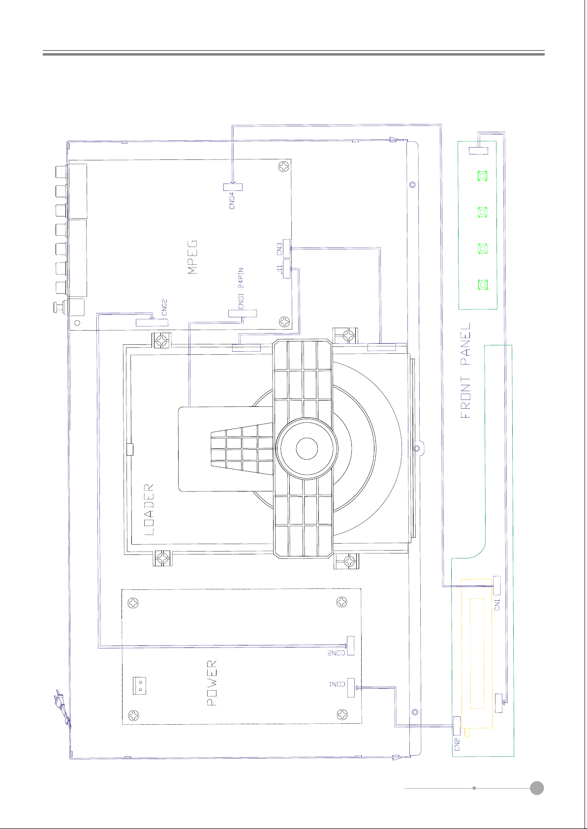
2. BLOCK DIAGRAM (CABLE CONNECTIONS)
2
Page 4
B
8
2
12345
JP
C
5
1234567
JP
D
A
1/1
4321
F+
V
CE3
10 0u/ 16
2
D4
FR 10
T1
V
F-
-2 4
k
R1 5
10
V
D9
6. 8
7
R1 4
4.
V
22 0u/ 35
CE6
2
FR 10
D5
-1 2V
V
F-
F+
5V
-2 1
V
CE9
V
0
D6
22 0UF/ 16
12
R1 3
27
V
V
-1 2
+1 2
1/ 4W
R3 4
1K
V
H
CE1 0
47 0u/ 16
L6
20 u
7
D7
FR 15
0
D8
SB 36
CA1
V
V
V
D5
-1 2V
D5 V
7
1N 400
D10
CE1 4
2
10
3. 3
+1 2
3. 3V
V
4
C2 4
10
V
V
47 0u/ 10
CE1 3
10 00u /10
22 0u/ 10
CE1 6
7
1N 400
D11
K
R1 7
10
0
47
R3 3
C2 2
K
R2 1
10
V
K
10 4/5 0
R2 2
20 0
C
TL4 31
IC3
SAV
0
52CA/A
1
IC
E
HGND
134 5
1T
SUF
2
678
2
VIPE R2
R6
1
2
1N
SW 1
21
0
K
2R
30
1
Vk1/
5C
2
IN4 007
BR1
BR
IN4 007
74
P0
F
4C
D
7
D1
FR 15
CE2
/u74
V004
4EC
4
BR3
IN4 007
BR
IN4 007
34
74
P0
F
L1
3C
2
D2
FR 10
V
22 u/3 5
4
C2 3
10
HGND
v
0. 1/27 5
12
C1
C
IC2
7
81
0
22
V
50/ 60HZ
AC 120- 220
C
B
HGND
A
1 2 3 4
Page 5
4. FUNCTIONAL DESCRIPTIONS
4.1 DVD MPEG board
4M FLASH
SERIAL
EPROM
CVBS
R
G
B
64M
SDRAM
SPCA8202
AUD2
AUD1
AUD0
5.1CHANNEL
AUDIO
Cntr/LFE
Rear L/R
Rear L/R
CODEC
DVD-DSP
I/F
CD-DSP
I/F
SPDIF
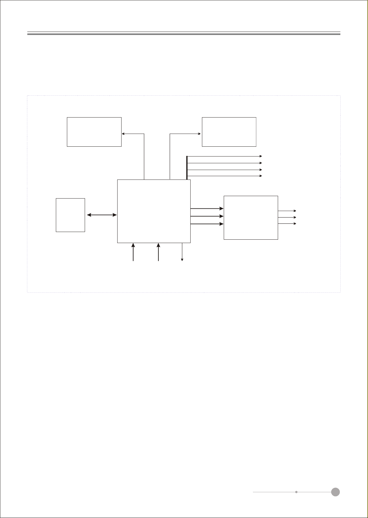
This board implements the back-end circuitry of a DVD player. It is composed of the following
subsystems:
* Microcontroller which does main control to all other sub-blocks of the system including user
interface, driver interface, audio/video output.
* Vaddis A/V Decoder IC decodes the bitstream coming from the DVD front-end drive, and
Optionally performs audio and video effects.
* Audio Codec
4
Page 6
5
A
2.2
R
M
BF01L
BF41L
BF
3
B
51C
FU1.0
R
D
NG
D
1
4004
N1
0
H
3
3 4
4
3
2
2
5
1
1
9
678
9
C
V5+
8C
B
U
1.0
F
NGF
D
+
V5
21CB
FU1.0
DNGM
CCVD
S
5CB
+
CE
5
FU1.0
U00
V61
F
1
NG
D
+V
V5
Am0
62
2
2
CE
CB
0
V61FU022
FU1.
DNGV
2
OT 5801SMA2U
52-
2
NI
CB
DNG
678
49
TU
O
ADJ
1
05753
S
MA3U
3
N
I
1
6
ADJ
FU1.
R
H
FU1.0
1
02273
A
A5+
A
V
BF02L
E
+
71
C
U001
V61F
DNGA
H
5
4
3
5
3
2
1
2435
1
9
9
C
5
678
5
H
678
59
U1
.0
F
2
R
D
V5+
P DNGFR
4CE
1CB
3
3
0
V61FU074
FP03
C C
NG
D
B
A
L
3
11C
9CB
B
3
FP3
FU1.
5
V5+ golana ovreS
V5+ ROTOM ovreS
V5+ metsy
V5+ reffub oediV
3
CCVD
43R
074
D
01
4004N1/CN
11D
4004N1/C
N
2
52-OT 5801
2
UO
T
81CCVD
71L
63R
074
S
BF92L
F
3L
B
0
51CE
CB
52
FU1
V61FU022
.0
D
NG
2
028
k
V8.1+
1
.
V
8
CC
F
B
01CE
+
FU022
V61
DNG
P 21CC
1+
V2
3
3
96R
+
CE
1
001
1FU
V6
DNG
4
B
91L
F
+
61C
E
V61FU001
e
olc
3CCV_D
43
3
CCV_MOR
V3.3+ MARDS
)1xM46(am85~am
V3.3+ hsalF
s
111
R
3
3
NG
B
12L
F
lenre
L
8.1CCV
PV
L
01511
R
B
02C
FU1.0
DNG
VA
+
E
41C
V61FU0
01
DNG
A
4
oediV
LLP
14CB
V8.1+
FU1.0
V21-P 21-CCV
A
366
3
R
3
C
C
E
E
+
+
V6
U001
1
1F
DNGADNG
F72L
B
B
13L
F
31
V61FU00
3
3LLP
V3
.
2.228R
92CB
FU1.0
NG
F
D
R
V3.3FR
2CB
6
0
FU1.
28
t
20
o
3CCVLLPA
04
CB
3
Am
FU1.0
D
3CCVV
5
63CB
+
CE
2
1
B
0
0
V61F
U001
FP00
DNGV
U
3.3LLP_BS
2
93C
C
+
4
E
FU001
FU1.
V61
DNG
A3CCV
6CB
4
24C
+
E
FU1.
1
V61F
U00
DNG_
DA
3
72CB
FU1
.0
DNGFR
V3.3+ LLP oiduA
lan
retnI
V3.
3+LLP
)ssapyb LLP(
V3.3+ FR
V3.3+ CAD oediV
6
5
V3.3+ DA
6
5
6
C
N
41NC
1
2
3
4
5
6
7
8
9
S
RAC
9NC
1
2
3
4
5
6
DFV/RI
/
01N
C
1
2
3
4
M5.2/NIP4/BSU
92CE
0
1
0
C
5N
1
2
3
4
5
6
IP6/EMA
G
AOC
X
O_V/R
C
R
FA
O_
B
U
/
LF
A
O
_Y/G5
C
5
O_1BVC
O_
5
rC
2
1
L
1
2
L
3
L
4
L
5
6
MM45.2/NIP6/REWOP
G
DN
_Y/G
RFA
LFA
D
M0.2/NIP9/T
M
M
M5.2/NIP6
94C
5C
F
3
P33
G
DN
M
+
96C
V61FU
N
C
DNGD
NG
V5+P
MM0.2/N
DNG
A
3V
O
C
3
_V
/
O
R
1
8
28
C
9
FU1.
FU1.0
0
DNG
RFA
6
B
O_U/
4
9C
C
0
19
.
U
FU1
F
.0
0
1
DNG
LF
A
9
O
_Y/G
7
29
C
39
FU1.
0
FU1.0
DNG
VA
5
2
7
8
DNGV
2
F5
B
V21-P
BF2
V21+P
BF8
V5+P
F1
B
V5+BSU
C
31N
V
1
V
2
3
4
5
6
7
5
O_1BVC
5
O_V/R
5
O
5
O_U/B
6
DNGV
6
5
EDOM_GIS
5
EDOM_SI
6C
1
5
3
FP3
27C
CN
DNG
R
9
5
4
3
1
6
4
9
7
1-K
CAJ-
2
VA
5
S
-
/pmoc
MM0.2/NIP7/AGV
52L
42L
36
C
FP3
FP33
22911R
22311R
R
411
K51
NG
D
G
76R
K
K7.
7.4
D
MAG
E
_
G
EMA
1
12
3
3
4
4
6
67
9
98
1
0
01
oediv
V5
+P
2
CNYS_V_
CNYS_V_V
2
CNYS_H_
CNYS_H_V
NGV
D
5
O_V/R
5
O_Y/
G
5
O_U/B
5
O_1B
VC
C
CVD
135
78
R
1N
1
iP 8(K
642
B
F62L
B
F
B
F
B
F22L
F32L
N
1D_
V
B
D
1 2
711R
K51
20
2
DNG
2
2
5
5
8
8
O_Y
DNG
I
CCVD
V5+P
R
6
5
022
31Q
N2
6093
6
6
DNG
V
5
troP gubeD
)R4 ,n
AD_DFV
2AT
2BTS_DFV
KLC_DFV
2
2NI_R
)Am005,6021(ESUF1F
V5+BSU
_BSU
DNG
6
84R
4R
022
.4
K7
1Q
2
6093N2
C
AXA
_
C
A
C_C
W
SA
W
SA6
RSA
R
SA6
A
RF
FA6
R
LS
A
LSA6
LFA
LFA
1VA
TUO
NCNC
CCV
DNG
NC NC
NC
7 8231
TUO ITPO
elti
T
P
S
C
S
a
1
D
11N
C
1
2
rewop draob draC
8NC
1
2
3
4
5
6
7
8
9
1
0
11
21
3
1
4
1
5
1
6
1
DRA
C
2MD_BSU
2PD
21NC
1
2
3
M
MM5.2/NIP3/CI
15R
4
K7.
2KLC_EMAG
G
HCTAL_EM
2
A
A
4V
3
3
1
1
6
6
4
4
9
9
7
7
-KCAJ-VA
1
O
O_ITP
6
4
5
P
O
T
O
DNG
V
3CCV
82LBF
NG
D
DN
G
2PW_DRAC
2KLC_SM
2SB_SM
DNG
2
SM
0D_
2
SM
1D_
22D_SM
D
NG
DNG
23D_SM
C
22ESNES_DRA
21ESNES_DRAC
2TSR_DRAC
D
NG
DNG
2R_CIM
DA
DNG_
2
L_CIM
2
2
5
5
8
8
D
GA
N
6O_I
DDV_ITP
YGOLONHCET SULPNUS
rotcennnoC & rewo
reb
muN tnemucoDezi
B-0-612-YS-61-S2028
h
ra
yadrut
c
M ,
1
15002 ,62
teehS:etaD f
R
ve
6
o
D
B
A
0.1
Page 7
5
TP1
RAD+
TP2
TP3
RAD-
FOC+
A+5V
TP4
BC66
0.01UF
RFGND
RF3.3V
+
R14
240
0
0
0
0
0
C
D
PUHRF
A
B
F
VREF1
BC4 0.1U
E
CDVR
DVD_VR#
PUH_CDLD#
DVDMDI
PUH_DVDLD#
BC3
0.1U
EC11
47UF16V
R57 0
0
0
0Samsung
0
0
0
R153
10K
Q25
3904
BC67
1000PF
FOC-
FOC- 4
FOC+ 4
RAD+ 4
RAD- 4
C97 NC
BC10 0.1U
R14 0
R15 0
L11 10UH
R31 0
L12 10UH
CD_VR
3 1
DVD_VR
31
RFGND
20K
2.2K
2.2K
2.2K
NOT SUPPORT AM5668 NOW
4.7K
NOT SUPPORT AM5668 NOW
2.2K
RESET_B
C87
0.1UF
DVCC3
BC44
0.1UF
GND
5
RFGND
RFGND
RFGND
2
Q3
2SK3018
Q4
2SK3018
R44 100K
2
PUH_DVDLD
Motor Driver AM5668
R62
1000P
24K
33K
1000P
1500P
12K
12K
1500P
BC50
0.1UF
1
2
3
4
5
6
7
8
26 25
27 28
CN4_SY
ELCO-CON24(Left)
BC18
0.1UF
RFGND
9
10
11
12
13
14
15
16
17
18
19
20
21
22
23
24
R39
5.1
Q7
2SB1132(R type)
D2
1N4148(SMT)
D D
C C
PUH_CDLD
Pickup head parameter
R40
R39
4.7
4.7
Sanyo
Mitsumi
Kenwood
B B
Thomson
EC36
10UF16V
R158
10K
A A
RF3.3V
BC32
0.1UF
RFGND
DVCC3
GND
5.1
5.1
5.1
5.1
+
R155 100
D9
1N4148(SMT)
BC24
0.1UF
BC30
0.1UF
5.1
5.1
5.1
5.1
5.1
A+5V
close to
connector!
CD_VR
DVD_VR
PUH_CDLD
CDMDI
PUH_DVDLD
R28 100K
BC7
0.1UF
RFGND
R65
NC(10K)
R81
NC(4.7K)
HFM SW
HOP1200W
OTHER
Q9
3904
3(C) 1(E)
R29
470
A+5V
R43
470
RF3.3V
R40
5.1
BC19
0.1UF
Q8
2SB1132(R type)
D3
1N4148(SMT)
RFGND
C33R15
R63
1000P
68KSony 39K
1000P
68K
68K
1000P5.1
68K
1000P
XT1
27MHz
R103
4.7K
C64
33PF
GND
VCC1.8 PLL3.3V
BC45
BC52
0.1UF
0.1UF
GND
+
EC7
100UF10V
A+5V
R41
13
NC
Q6
2
NC(9015 DIP)
R45
HFM
NC(1K)
R245
HFM SW
NC
as above
0
NC
2(B)TOP CONTACT
RFGND
LDSW
+
EC12
47UF16V
DVDLDOCDLDO
R58 0
Motor Driver AT5660
R62R53
10K
20K
3.3K
3.3K
8.2K
3.3K
CLKOUT
CLKIN
C65
33PF
BC28
0.1UF
C32C32
1500P
1000P
2700P
2700P
1500P
2700P
BC46
0.1UF
R63
39K
39K
39K
91K
12K
BC51
0.1UF
ELCO-CON24(buttom)
4
A+5V
CN4_HI
1
2
3
4
DVDMDI
5
HFM
6
R26 100
7
8
9
10
11
12
13
14
15
16
17
18
19
20
21
22
23
24
26 25
Hitachi Bottom CONTACT
SANYO
MITSUMI
VREF24
C33
1000P
1000P
1000P
1000P
1000P
1500P
BC53
0.1UF
CDMDI
RFGND
A
C DPDA
BC21
0.1UF
RFGND
MGND
BC68
BC31
1000PF
0.1UF
RFGND
4
PUH_DVDLD#
PUH_CDLD#
R1 100
C12
680P
C13
680P
C30NCC100
NC
680P
+
C27 0.1UF
RAD- 4
RAD+ 4
FOC- 4
FOC+ 4
BC62 0.1U
BC23 0.01U
PUHRF
C
B
A
D
E
F
VREF1
TP11RFIP
DPDC
NC
C101
680P NC680P
NC
RFGND
EC9
47UF16V
RFGND
TCO4
RFGND
FCO4
SPDCO4
C26 0.1UF
SCO4
TRAY-4
TRAY+4
DMEA4
HOME4
VVCC3
BC37
0.1UF
VGND
BC67 0.01U
C32
680P
EC8 47UF16V
BC22 0.1UF
RFGND
C22 1000PF
RFGND
C33 1000PF
C32 1000PF
RF3.3V
RFGND
RFGND
RFGND
RFGND
RFGND
PUHRF
C42 NC(120PF)
C41 680PF
C38 680PF
C40 680PF
C37 680PF
CDA
+
RFGND
TP5RFCT
C31 300PF
R38 470K
C29 330PF
TRAYOUT4
R42 4.7K
TP8CDB
TP9
TP7F
TP6E
RFGND
RF3.3V
RFGND
C34 0.01UF
C30 0.047UF
C28 820PF
RFGND
RF3.3V
RFGND
TRAYIN4
TP10FGIN
C98 NC/100PF
RFIP
C39
1UF
DPDA
DPDC
D
C
B
A
CDB
CDA
F
E
DVDLDO
CDLDO
DVDMDI
CDMDI
VREF1
R64 33K (1%)
C36 0.22UF
C35 0.01UF
XOPVIP1
XOPVIN1
XOPOP1
R63 68K
R62 33K
TRAYIN
TRAYOUT
R54 2.2K
R53 2.2K
FGIN
LDSW
RFCT
SBAD
FEO
TEO
RFGND
RFGND
C46 680PF
C52 0.01UF
TP24
RFRP
C45 1UF
C50 1UF
U7
1
AGCON
2
AGCOP
3
RFIP
4
RFIS
5
RFSUM
6
DPDA
7
DPDB
8
DPDC
9
DPDD
10
DVDD
11
DVDC
12
DVDB
13
DVDA
14
CDB
15
CDA
16
CDF
17
CDE
18
RF_AVSS
19
APC_AVSS
20
DVDLDO
21
CDLDO
22
DVDMDI
23
CDMDI
24
APC_SRV_AVDD
25
V21
26
R33K
27
V165
28
SVOTST
29
RFRPPH
30
RFRPBH
31
RFRPMEAN
32
SBADPH
33
SBAD
34
FEO
35
TEO
36
TEOLP
37
OPVIP
38
OPVIN
39
OPVOP
40
SRV_AD_AVSS_VRGD
41
AD_DA_AVDD
42
DATEO
43
DAFEO
44
DA_AVSS
45
TRAY_IS_IN
46
TRAY_IS_OUT
47
SPDC_OUT/GPIO
48
SC_OUT/GPIO
49
SC1_OUT/GPIO
50
TRAY_OUT/GPIO
51
DMEA/GPIO
52
FGIN/GPIO
53
HOMESW/GPIO
54
LDSW/GPIO
TP12
DFCT
3
Vref0
PD
C54 47PF
C51 1UF
R94 1.5K
RFI
R96 20K
RFO
216
FLTIN
C47 0.068UF
C62 100PF
RFGND
C56 0.1UF
RFRP
215
214
213
RFO
FLTIP
RFRP
C53 47PF
R104 5.1K
R97 5.1K
RF3.3V
PLL3.3V
R93 1.2K (1%)
212
211
210
209
GMRES
AGCCAP
RF_AVDD
DS_AVDD
FD
LGIN
C57 0.01UF
R105 150K
VVCC3
VVCC3
VVCC3
VGND
VGND
RFGND
208
207
206
205
204
203
202
201
200
199
198
LGIN
PLL_DS_AVSS
197
LPFN
LPFO
FDFLT
PDFLT
VREFO
LPFNIN
RFI
SLVL
CNIN
VGND
PLL3.3V
V_COMP
V_BIAS
TV_DAC0
V_FSADJ
V_V_SYNC
V_REF
TV_DAC4
TV_DAC3
TV_DAC5
196
195
194
193
192
191
190
189
188
187
186
185
184
183
182
V_BIAS
V_COMP
TV_DAC5
VSS_TVA2
PLL_AVDD
VDD_TVA2
V_FSADJ
TV_DAC4
TV_DAC3
TV_DAC0
VSS_TVA1
VSS_TVA0
VDD_TVA1
VDD_TVA0
V_REFOUT
SPHE8202S
DFCT/GPIO
VDD_K1
GPIO/SD_CK/MS_CK
GPIO/SD_CMD/MS_BS
GPIO/ttio0_4/SD_D0/MS_D0
VSS_O1/VSS_K1
GPIO/ttio1_5/SD_D1/MS_D1
GPIO/ttio2_6/SD_D2/MS_D2
GPIO/ttio3_7/SD_D3/MS_D3
VDD_O1
GPIO
R_CS4_B/GPIO
R_CS3_B/GPIO
R_CS2_B/GPIO
R_CS1_B/GPIO
RST_B
IR_IN/GPIO
VFD_CLK/GPIO
VFD_STB/GPIO
VFD_DATA/GPIO
R_20/E_MX10
R_A19
CLKIN
CLKOUT
USB_GND
USB_VDD
USB_DP
USB_DM
VSS_PLLA
VDD_PLLA
VSS_PLLV
VDD_PLLV
M_D7
555657585960616263646566676869707172737475767778798081828384858687888990919293949596979899
DFCT
R90
RF3.3V
0
CARD_RST
MS_D0
MS_CLK
MS_BS
GND
VCC1.8
L35 FB
PIN_142
PIN_141
PIN_125
RF3.3V
3
MS_D1
MS_D2
R173 0
R175 0
R177 0
I2C_CLK
MS_D3
CARD_SENSE2
CARD_SENSE1
R49 4.7K
R47 4.7K
IR_IN
RESET_B
R_CS1
VFD_DATA
CLKOUT
VFD_CLK
VFD_STB
DQM2
DQM3
M_BA1
TRAYIN
TRAYOUT
CLKIN
CARD_WP
RA19
GND
RESET_B 3,6
I2C_DATA
M_D6
MD7
MD6
MD5
USB_DP
USB_DM
GND
GND
APLLVCC3
USB_PLL3.3
VPLLVCC1.8
AD_REF
GND
AU_XCK
V_H_SYNC
AU_BCK
AU_LRCK
181
180
179
178
177
A_XCK/GPIO
A_BCK/GPIO
UA0_TX/GPIO
UA0_RX/GPIO
VSS_K6/VSS_O6
M_D5
M_D4
M_D3
VDD_O2
M_D2
MD3
MD4
MD2
MD1
DVCC3
USB_DM 1
USB_DP 1
C103
0.1UF
AD_GND
A_LRCK/GPIO
M_D1
AUDIO_MUTE
176
MD0
2
VCC3A
DVCC3
AD_GND
RA16
RA18
SPDIF_OUT
AU_D0
AU_D1
AU_D2
175
174
173
172
VDD_O5
A_DATA3/GPIO
A_DATA2/GPIO
A_DATA1/GPIO
M_D0
M_WE_B
M_CAS_B
M_RAS_B
M_CAS
M_RAS
MWE
GND
171
A_DATA0/GPIO
A_IEC_TX/GPIO
VSS_O2/VSS_K2
M_CS0_B/GPIO
100
M_CS0
RA15
AD_REF
AD_R
AD_L
170
169
168
167
164
166
165
163
AD_L
AD_R
R_A18
R_A16
R_A15
AD_VSS
AD_REF
AD_VDD
VSS_O5/VSS_K5
M_DQM2/GPIO
M_DQM3/GPIO
VSS_O4/VSS_K4
M_BA1/GPIO
M_DQM0/GPIO
M_DQM1/GPIO
M_CKE/GPIO
VSS_O3/VVV_K3
M_A11/GPIO
M_BA0
M_D15
M_D14
M_D13
VDD_K2
M_D12
M_D11
M_D10
101
102
103
104
105
106
107
108
M_BA0
MD14
MD11
MD15
MD13
MD12
MD10
VCC1.8
2
R_A12
R_OE_B
VDD_K4
R_A10
R_A11
VDD_O4
R_A13
R_A14
R_A17
R_WE_B
M_A10
VDD_K3
M_CLKO
VDD_O3
R_A7
R_A6
R_A5
R_A4
R_A3
R_A2
R_A1
R_A0
R_D0
R_D1
R_D2
R_D3
R_D4
R_D5
R_D6
R_D7
R_A9
R_A8
M_A3
M_A2
M_A1
M_A0
M_A4
M_A5
M_A6
M_A7
M_A8
M_A9
M_D8
M_D9
RA12
162
RA7
161
RA6
160
RA5
159
RA4
158
RA3
157
RA2
156
RA1
155
RA0
154
RD0
153
RD1
152
RD2
151
150
149
148
147
146
145
144
143
142
141
140
139
138
137
136
135
134
133
132
131
130
129
128
127
126
125
124
123
122
121
120
119
118
117
116
115
114
113
112
111
110
109
RD3
RD4
RD5
RD6
RD7
ROE
PIN_142
PIN_141
RA10
RA11
RA9
RA8
RA13
RA14
RA17
RWE
MA3
MA2
MA1
MA0
MA10
PIN_125
DQM0
DQM1
MA4
MA5
MA6
MA7
MA8
MA9
M_CKE
MA11
MD8
MD9
AD_R
AD_L
GND
VCC1.8
DVCC3
GND
VCC1.8
M_CKE 3
GND
SDRAM_CLK 3
DVCC3
VCC3A
D12
1N4148(SMT)
C99 0.47UF
VCC3A
D13
1N4148(SMT)
CARD_RST
CARD_SENSE1
CARD_SENSE2
MS_D0
MS_D1
MS_D2
MS_D3
R240 470
R241
C100
330
0.001UF
AD_GND
R242 470
C101 0.47UF
R243
C102
330
0.001UF
AD_GND
SUNPLUS TECHNOLOGY
Title
DSP
Size Document Number Rev
8202S-16-SY-216-0-B
Date: Sheet
AVCC-12
NJM4558
AVCC-12
NJM4558
1
ROE
RWE
R_CS1
AU_LRCK
AU_BCK
AU_XCK
SPDIF_OUT
TV_DAC5
TV_DAC4
TV_DAC3
TV_DAC0
V_BAIS
V_COMP
V_REF
V_FSADJ
V_V_SYNC
V_H_SYNC
XOPVIP1
XOPVIN1
XOPOP1
VFD_DATA
VFD_STB
IR_IN
VFD_CLK
AU_D0
AU_D1
AU_D2
AUDIO_MUTE
R89 NC
R85 NC
R80 NC
R52 NC
R61 NC
R60 NC
R68 NC
MS_CLK
MS_BS
MS_D0
MS_D1
MS_D2
MS_D3
CARD_SENSE1
CARD_SENSE2
CARD_RST
CARD_WP
I2C_DATA
I2C_CLK
M_CS0
M_CAS
M_RAS
MWE
M_BA0
M_BA1
R135100K
1
U19A
AVCC12
7
U19B
1
R133100K
AVCC12
C21100p
-
+
8 4
C20100p
-
+
8 4
2
3
AGND
6
5
AGND
RA[0..19] 3
RD[0..7] 3
ROE 3
RWE 3
R_CS1 3
AU_LRCK 6
AU_BCK 6
AU_XCK 6
SPDIF_OUT 6
TV_DAC5 5
TV_DAC4 5
TV_DAC3 5
TV_DAC0 5
V_BIAS 5
V_COMP 5
V_REF 5
V_FSADJ 5
V_V_SYNC 1
V_H_SYNC 1
XOPVIP1 4
XOPVIN1 4
XOPOP1 4
VFD_DATA 1
VFD_STB 1
IR_IN 1
VFD_CLK 1
AU_D0 6
AU_D1 6
AU_D2 6
AUDIO_MUTE 6
SCART_SIG 5
SCART_DISPLAY 5
RELEASE_SCART 5
GAME_CLK 1
GAME_LATCH 1
GAME_D0 1
GAME_D1 1
MS_CLK 1
MS_BS 1
MS_D0 1
MS_D1 1
MS_D2 1
MS_D3 1
CARD_SENSE1 1
CARD_SENSE2 1
CARD_RST 1
CARD_WP 1
SP_SDA 3
SP_SCL 3
MD[0..15] 3
MA[0..11] 3
DQM[0..3] 3
M_CS0 3
M_CAS 3
M_RAS 3
MWE 3
M_BA0 3
M_BA1 3
R132
10K
C19
820P
AGND
R126
10K
820P
C14
AGND
26Saturday, March 26, 2005
MIC_R
1
MIC_L
1
1.0
of
Page 8
5
4
3
2
1
U14
A0
A1
A2
A3
A4
A5
A6
A7
A8
A9
A10
A11
A12
A13
A14
A15
A16
A17
A18
CE
OE
A19
AM27C040/AM27c080(DIP)
13
D0
14
D1
15
D2
17
D3
18
D4
19
D5
20
D6
21
D7
32
VCC
16
GND
33
/WE
34
/RST
FLASH_POWER
GND
DVCC
R148
0
12
11
10
9
8
7
6
5
27
26
23
25
4
28
29
3
2
30
31
22
24
1
R166 NC
R165 0
RA1
RA2
RA3
D D
C C
RA4 RD4
RA5
RA6
RA7
RA8
RA9
RA10
RA11
RA12
RA13
RA14
RA15
RA16
RA17
ROM_PIN31
R_CS1
ROE
RA19
ROM_VCC3
RD0
RD1 RD1
RD2
RD3
RD4
RD5
RD6
RD7
FLASH_POWER
RWE
RESET_B
0.1UF
GND
DVCC
040 OTP
C83 10PF
GND
SDRAM_CLK2
MA0
MA1
MA2
MA3
MA4
MA5
MA6
MA7
B B
MA8
MA9
MA10
M_BA0 M_BA0
RAM_CLK
M_CKE
M_CS0 M_CS0
M_RAS M_RAS
MWE
DQM0
DQM1
A A
R141 33
21
A0
22
A1
23
A2
24
A3
27
A4
28
A5
29
A6
30
A7
31
A8
32
A9
20
A10
19
BA/A11
35
CLK
34
CKE
18
CS
17
RAS
16
CAS
15
WE
36
DQMHNCVCCQ
33
NC
37
26
VSS
50
VSS
SDRAM 16M-6(512Kx16x2)
GND
U13
RAM_CLK
RN3 33(8 Pin, 4R)
D0
2
DQ0
D1
3
DQ1
D2
5
DQ2
D3
6
DQ3
D4
8
DQ4
D5
9
DQ5
D6
11
DQ6
D7
12
DQ7
D8
39
DQ8
D9
40
DQ9
D10
42
DQ10
DQ11
DQ12
DQ13
DQ14
DQ15
VCCQ
VCCQDQML
VCCQ
VSSQ
VSSQ
VSSQ
VSSQ
5
D11
43
D12
45
D13
46
D14
48
D15
49
1
VCC
25
VCC
7
1314
38
44
4
10
41
47
GND GND GND
080 ROM NC
FLASH NC
7
8
5
6
3
4
1 2
RN5 33(8 Pin, 4R)
7
8
5
6
3
4
1 2
SD_VCC3
SD_VCC3
EC35
+
100UF16V
GND
RA0
RA1
RA3
RA4
RA5
RA6
RA7
RA8
RA9
RA10
RA11
RA12
RA13
RA14
RA15
RA16
RA17
RA18
R156 0
RWE
R159 NCBC61
R_CS1
ROE
RA18
R154 NC
R225
NC
NC NC
NC 0
0NC
RN2 33(8 Pin, 4R)
7
8
5
6
3
4
1 2
RN4 33(8 Pin, 4R)
7
8
5
6
3
4
1 2
BC56
0.1UF
BC58
0.1UF
U15
12
A0
11
A1
10
A2
9
A3
8
A4
7
A5
6
A6
5
A7
27
A8
26
A9
23
A10
25
A11
4
A12
28
A13
29
A14
3
A15
2
A16
30
A17
ROM-A18
31
A18
22
CE
24
OE
ROM-A19
1
A19
AM27C040/Flash MX29F040(PLCC)
R166 R148R165
0
D0
D1
D2
D3
D4
D5
D6
D7
VCC
GND
R159
R156 R154
NC
0
NC
MA0
MA1
MA2
MA3
MA4
MA5
MA6
MA7
MA8
MA9
MA10
RAM_CLK
M_CKE
M_CASM_CAS
MWE
DQM2
DQM3
0
MD0
MD1
MD2
MD3
MD4
MD5
MD6
MD7
MD8
MD9
MD10
MD11
MD12
MD13
MD14
MD15
4
NC
BC49
0.1UF
RD0RA0
13
14
RD2RA2
15
RD3
17
18
RD5
19
RD6
20
RD7
21
FLASH_POWER
32
16
GND
NC0
NC
0
0
U16
21
A0
22
A1
23
A2
24
A3
27
A4
28
A5
29
A6
30
A7
31
A8
32
A9
20
A10
19
BA/A11
35
CLK
34
CKE
18
CS
17
RAS
16
CAS
15
WE
36
DQMHNCVCCQ
33
NC
37
26
VSS
50
VSS
SDRAM 16M-6(512Kx16x2)
DQ0
DQ1
DQ2
DQ3
DQ4
DQ5
DQ6
DQ7
DQ8
DQ9
DQ10
DQ11
DQ12
DQ13
DQ14
DQ15
VCC
VCC
VCCQ
VCCQDQML
VCCQ
VSSQ
VSSQ
VSSQ
VSSQ
2
3
5
6
8
9
11
12
39
40
42
43
45
46
48
49
1
25
7
1314
38
44
4
10
41
47
R225
0
NC
D0
D1
D2
D3
D4
D5
D6
D7
D8
D9
D10
D11
D12
D13
D14
D15
SD_VCC3
3
MA0
MA1
MA2
MA3
MA4
MA5
MA6
MA7
MA8
MA9
MA10
MA11
DQM0
DQM1
MWE
M_CAS
M_RAS
M_CS0
M_CKE
RAM_CLK
M_BA0
M_BA1
U11
23
A0
24
A1
25
A2
26
A3
29
A4
30
A5
31
A6
32
A7
33
A8
34
A9
22
A10/AP
35
A11
15
LDQM
39
UDQM
16
WE
17
CAS
18
RAS
19
CS
37
CKE
38
CLK
20
BA0
21
BA1
6
VSSq
12
VSSq
46
VSSq
52
VSSq
GND
SDRAM 1Mx16x4
EliteMT M12L64164A-5T
54-Pin TSOPII(400mil x 875mil)
RA1
RA2
RA3
RA4
RA5
RA6
RA7
RA8
RA9
RA10
RA11
RA12
RA13
RA14
RA15
RA16
RA17
RA18
RA19
R_CS1
ROE
GND
D10
D11
D12
D13
D14
D15
NC/RFU
VSS
VSS
VSS
VDD
VDD
VDD
VDDq
VDDq
VDDq
VDDq
RWE
D0
D1
D2
D3
D4
D5
D6
D7
D8
D9
NC
2
RWE2
RESET_B2
U17
48
A16
17
A17
16
A18
26
CE
28
OE
11
WE
12
RST
47
BYTE
MX29LV800T/B,MX29F800T/B
TSOP-48
MD0
2
MD1
4
MD2
5
MD3
7
MD4
8
MD5
10
MD6
11
MD7
13
MD8
42
MD9
44
MD10
45
MD11
47
MD12
48
MD13
50
MD14
51
MD15
53
36
40
28
41
54
1
14
27
3
9
43
49
GND
SD_VCC3
Title
Size Document Number Rev
DQ0A0
DQ1A1
DQ2A2
DQ3A3
DQ4A4
DQ5A5
DQ6A6
DQ7A7
DQ8A8
DQ9A9
DQ10A10
DQ11A11
DQ12A12
DQ13A13
DQ14A14
DQ15/A-1A15
NC
NC
NC
NC
RY/BY
VCC
GND
GND
1
A0
2
A1
3
A2
4 5
GND SDA
24C01/CAT24C021
GND
I2C ADDR = 0XA0
SD_VCC3
BC60
BC57
0.1UF
0.1UF
GND
SUNPLUS TECHNOLOGY
ROM/FLASH/Memory
8202S-16-SY-216-0-B
Date: Sheet
ROM_D0
2925
ROM_D1
3124
ROM_D2
3323
ROM_D3
3522
ROM_D4
3821
ROM_D5
4020
ROM_D6
4219
ROM_D7
4418
308
327
346
365
394
413
432
RA0
451
9
10
13
14
15
37
46
27
U5
VCC
WP
SCL
DVCC
GND
BC59
0.1UF
BC34
0.1UF
8
7
6
GND
BC43
0.1U
GND
RESET_B
M_CS0
M_CAS
M_RAS
MWE
M_CKE
M_BA0
M_BA1
ROE
RWE
R_CS1
DVCC
GND
FLASH_POWER
DVCC
R92
R95
1K
1K
1
SP_SCL 2
SP_SDA 2
RESET_B 2,6
MA[0..11] 2
MD[0..15] 2
DQM[0..3] 2
M_CS0 2
M_CAS 2
M_RAS 2
MWE 2
M_CKE 2
M_BA0 2
M_BA1 2
RA[0..19] 2
RD[0..7] 2
ROE 2
RWE 2
R_CS1 2
36Saturday, March 26, 2005
of
1.0
Page 9

5
U4
AM5888
DIP28-SSOPH
VREF2
BC17
0.1UF
FCO
TR_B1
REGO2
TCO
MGND
SPDCO
D D
C C
TR_B2
0R203
1
VINFC
BIAS
2
3
26
27
25
24
CFCerr1
CFCerr2
VINTK
BIAS
CTKerr1
CTKerr2
7.5K
10K
7.5K
BIAS
4
VINSP
BIAS
SCO
M+5V
TRAY-
M+5V
EC6
100UF16V
DMEA 2
TRAYOUT 2
TRAYIN 2
HOME 2
XOPVIP1 2
XOPVIN1 2
XOPOP1 2
VREF2 2
BC14
0.1UF
M+5V
BC6
0.1UF
MGND
DMEA
TRAYOUT
TRAYIN
HOME
XOPVIP1
XOPVIN1
XOPOP1
VREF2
5
B B
A A
23
VINSL
0R21
21
VCTL
6 9
FWD VOLD-
7
REV
8
Vcc1
19
Vcc2
MGND
FOC+
FOCRAD+
RAD-
TCO
FCO
SCO
SPDCO
TRAYTRAY+
10K
4
20K
+
20K
+
10K
10K
PreDriver
PreGND
GND1
22
29
MGND
FOC+ 2
FOC- 2
RAD+ 2
RAD- 2
TCO 2
FCO 2
SCO 2
SPDCO 2
TRAY- 2
TRAY+ 2
4
+
-
25K
+
-
15K
3
14
+
Driver
VOFC+
VOFC-
13
0R7
FOC+
FOC-
2
1
-
X2
7.5K
+
Driver
VNFFC
VOTK+
VOTK-
-
X2
7.5K
Driver
Driver
Tray
Driver
GND2
30
VNFTK
VOSP+
VOSP-
VOSL+
VOSL-
VOLD+
CN3
6PIN/2.0MM
CN2
5PIN/2.0MM
STBY
5
4
3
2
1
1
2
3
4
5
6
5
15
16
20
12
11
17
18
28
10
SLED+
SLED-
SP+
SP-
LOADLOAD+
REGO1
HOME 2
MGND
TRAYOUT 2
MGND
TRAYIN 2
3
RAD+
0R4
0R19 R27 150K
0R12
RAD-
SP+
SP+SNSR XOPVIP1
SP-
SLEDSLED+
DMEA
LOAD-TRAY+
LOAD+
R23 1
R22 150K
XOPVIN1 XOPOP1
Motor Driver Parameter
R13 R19 R12 R18 R7 R8 R4 R6 R30 R32 C15 C17
AT5660 & AT5665
0NCNC01111 22K 22K 330p 330p
AM5668
AT5660 & AM5668
AT5665
00
NC NC
2
VREF2
R33
C18
470K
4700PF
R25 470K
C16 4700PF
21
D5
1N4004,DIP
Q23
2SS8550D
REGO1 REGO2
13
2
R137
4.7K
R147
10K
Q10
2SS8550D
13
R125
R136
D4
1N4004,DIP
2
20K
12K
TR_B2TR_B1
DVCC3DVCC18
NC NC NC NC00NCNC 0 0NC NC
R202 R203R201 R204
NC
NC
00
SUNPLUS TECHNOLOGY
Title
Motor-Driver
Size Document Number Rev
B
8202S-16-SY-216-0-B
Date: Sheet
21
D+5V 1,2,4,5
R248
0
NC
1.0
46Saturday, March 26, 2005
1
of
Page 10

5
4
3
2
1
VVCC3
CVB1
G/Y
B/U
D D
R55
75
R24
150
R17
150
R16
150
R/V
TV_DAC0 2
TV_DAC3 2
TV_DAC4 2
TV_DAC5 2
VGND
VVCC3
VGND
VGND
1/2 current config
VGND
V+5V
R50
75(DIP,1/4W)
C C
B B
CVB1
G/Y
13
2
R169 NC
V+5V
13
2
VGND
R246 NC
Q11
9015(DIP EBC)
R20
75(DIP,1/4W)
Q5
9015(DIP EBC)
C24 10PF
L18 1UH
C23
100PF
C10 10PF
L13 1UH R70
C9
100PF
VGND
CVB1_O
C25
100PF
G/Y_O/SY
C11
100PF
R/V
B/U
V+5V
13
2
VGNDVGND
R245 NC
V+5V
13
2
VGND
R247 NC
R3
75(DIP,1/4W)
Q1
9015(DIP EBC)
R9
75(DIP,1/4W)
Q2
9015(DIP EBC)
C74 NC
C70 0.1UF
C73 0.1UF
C71 0.1UF
R118 680
1/2 current config
V_BIAS 2
V_COMP 2
V_REF 2
V_FSADJ 2
C2 10PF
L6 1UH
C1
100PF
C7 10PF
L9 1UH
C6
100PF
VGND
VGNDVGND
R/V_O/SC
C3
100PF
B/U_O
C8
100PF
SCART_DISPLAY
TV0
CVB
CVB
CVB
SCART_SIG
R79 4.7K
R78
4.7K
R71
4.7K
Q14
9014
TV4
CVB
GND
Cb
B
Q15
9014
R87
68
Q16
9014
R83
82
GND
TV3
Y
Y
(S-Video)
GR
DVCC
R88
4.7K
R84 120
P+12V
GND
TV5
Cr
(S-Video)
SIGNAL_MODE
180
R72 4.7K
C
DISPLAY_MODE
RELEASE_SCART
R17
75
150
R24
75
150
Not RELEASE
RELEASE1
0
R246
0390
NC NC
R247R245
75
0
150
3
VIDEO DAC
SCART_SIG
SCART_DISPLAY
RELEASE_SCART G/Y_O/SY
A A
SIGNAL_MODE
DISPLAY_MODE
SCART_SIG 2
SCART_DISPLAY 2
RELEASE_SCART 2
SIG_MODE 1
DIS_MODE 1
5
CVB1_O
R/V_O/SC
B/U_O
CVB1_O 1
G/Y_O 1
Y_O 1
R/V_O 1
Cr_O 1
B/U_O 1
Full Current 0
Half Current NC
4
R169
R118 R16
680
NC
RELEASE_SCART0DISPLAY_MODE
SCART_SIG SIGNAL_MODE
0
1 3V(RGB)
2
0V(CVBS)
SUNPLUS TECHNOLOGY
Title
Video Buffer
Size Document Number Rev
B
8202S-16-SY-216-0-B
Date: Sheet
SCART_DISPLAY
1
0
DISPLAY_MODE
12V(9.5V--12V 4:3)
6V(5V--8V 16:9)
56Saturday, March 26, 2005
1
of
1.0
Page 11

5
4
3
2
1
C58
820PF
AGND
C43
820PF
AGND
R144 10K
C84
820PF
AGND
R129 10K
C78
820PF
AGND
AGND
AGND
3
R99 39K
C59 100PF
R100
2
10K
3
AGND
R74 39K
C44 100PF
R75
6
10K
5
AGND
R143 39K
C85 100PF
2
3
AGND
R128 39K
C79 100PF
6
5
AGND
R121 39K
C76 100PF
R122
10K
C75
820PF
AGND
R107 39K
C67 100PF
R108
10K
C66
820PF
AGND
AVCC12
AVCC12
AVCC12
AVCC12
2
3
6
5
-
+
8 4
-
+
8 4
-
+
8 4
-
+
8 4
-
+
8 4
AVCC12
-
+
8 4
AVCC12
AVCC-12
1
U6A
NJM4558
AVCC-12
7
U6B
NJM4558
AVCC-12
1
U12A
NJM4558
AVCC-12
7
U12B
NJM4558
AVCC-12
AVCC-12
AVCC12
AGND
AVCC12
AGND
1
U8A
NJM4558
7
U8B
NJM4558
EC21
10UF16V
+
AVCC-12
BC35
BC33
0.1UF
0.1UF
AGND
EC18
+
10UF16V
EC34
10UF16V
AVCC-12
BC55
BC48
0.1UF
0.1UF
AGND
EC31
10UF16V
10UF16V
AVCC12 AVCC-12
BC38
0.1UF
AGNDAGND
10UF16V
AGND
AGND
+
+
EC28
EC23
+
BC43
0.1UF
+
R101
10K
R76
10K
AGND
AGND
AGND
AGND
R145
10K
R130
10K
R109
10K
R102 100
R91 470
R77 100
R86 470
R146 100
R140 470
R131 100
R134 470
R123
10K
R110 100
R112 470
R124
100
R116
470
2N3904
2N3904
2N3904
2N3904
2N3904
2N3904
Q18
AGND
AGND
Q17
AGND AGND
Q22
AGND
AGND
Q21
AGND
AGND
Q20
AGND
AGND
Q19
AGND
AGND
2
ASW
C60
47PF
AC_C
AFR
C77
47PF
C68
47PF
C48
47PF
C86
47PF
AFL
C80
47PF
ASR
ASL
P+5V
ZD1
AGND
P+5V
P+12V
AGND
AUDIO_MUTE2
R167
2.2K
Zener / 5V1(dip)
+
EC37
220U16V
AGND
P+5V
R160 NC/200
R161 100
R231 10K
Title
Size Document Number Rev
Date: Sheet
P+5V
R164
7.5K
R163 10K
Q28
1 3
R162 10K
R157 470
2
C88
1UF
SUNPLUS TECHNOLOGY
Audio Filter
C
8202S-16-SY-216-0- B
Q27
1 3
2
2N3906
Q26
1 3
AGND
2N3906
Power On
Mute
Power
Off
Mute
2N3906
2
EC38
+
10U16V
1
66Saturday, March 26, 2005
1.0
of
+5AVAA
GND AGND
C81
0.1UF
GND
GND
RESET_B2,3
D D
C C
Audio Format:
ML,MC=00=> RJ 24 bit
ML,MC=01=> RJ 20 bit
ML,MC=10=> I2S 16 bit
ML,MC=11=> I2S 24 bit
B B
AU_D1
AU_D0
AU_BCK
AU_LRCK
AU_XCK
+5AVAA
+5AVAA
P+5V
GND
Audio Format:
ML,MC=00=> RJ 24 bit
ML,MC=11=> I2S 24 bit
8
DVDD
9
DGND
11
DIF1
12
DIF0
13
M1
15
M2
14
VLC
10
RST
1
VLS
2
DIN1
3
DIN2
4
DIN3
5
SCLK
6
LRCK
7
MCLK
AUDIO_MUTE
AU_XCK
AU_BCK
AU_LRCK
AU_D1
AU_D2
AU_D3
U10
AVDD
AGND
MUTE1
MUTE2
MUTE3
OUT1L
OUT1R
OUT2L
OUT2R
OUT3L
OUT3R
FILT+
VQ
CS4360
U11
1
AVDD1
DVDD
AVDD2
11
DGND
10
AGND1
LRCIN2
AGND2
14
13
12
GR0
MD/DM
GR1
MC/IWL
ML/12S
GR2
8
MODE
9
MUTE
OUT0R
2
SCKI
OUT0L
3
BCKIN
OUT1R
4
LRCIN
OUT1L
5
DIN0
OUT2R
6
DIN1
OUT2L
7 16
DIN2 CAP
WM8746/DA1196
AU_BCK
AU_LRCK
AU_XCK
22
21
28
25
18
27
26
24
23
20
19
A_CAP
16
17
EC32
BC47
10UF16V
0.1UF
AGND
+5AVAA
15
28
20
24
26
22
18
27
25
23
21
19
17
+
U9
1
SDATA
2
DEM/SCLK
3
LRCK
4 5
MCLK AOUTR
CS4334
+
EC29
10U16V
AOUTL
AGND
C_CAU_RST
SW
SL
SRAU_D2
F_L
F_R
F_R
F_L
SR
SL
SW
C_C
AGND
VA
+5AVAA
AGND
EC33
+
10UF16V
F_R 8
F_L 8
SR 8
SL 8
SW 8
C_C 8
BC54
0.1U
8
7
6
BC42
0.1UF
AGND
F_LAU_D0
F_R
BC54
0.1UF
+5AVAA
AGND
SW
10UF16V
C_C
F_R
10UF16V
F_L
10UF16V
EC19
+
10UF16V
EC30
+
EC27
+
20K
R73
20K
R142
20K
R127
20K
R98
EC20
+
CS4334 I2S format only
Replace GND
with VGND For
Himage
mechanism
ASW
AC_C
AFR
AFL
ASR
ASL
A A
AU_D0
AU_D1
AU_D2
AU_LRCK
AU_BCK
AU_XCK
ASW 1
AC_C 1
AFR 1
AFL 1
ASR 1
ASL 1
AU_D0 2
AU_D1 2
AU_D2 2
AU_LRCK 2
AU_BCK 2
AU_XCK 2
5
DVCC
BC1
0.1UF
VGND
DVCC OPTI_VDD
L4 FB
CS4360 Format
DIF1
0 LJ 24 bits
1
C4
0.1UF
VGND
DIF0
0
10
0
11
AUDIO INTERFACE
I2S
RJ 16bits
RJ 24 bits
R5 33
R10
200
R11
100
VGND
C96 0.1UF
C5
10PF
4
OPTI_O
COAX
OPTI_O 1SPDIF_OUT2
COAX 1
EC26
R120
+
SR
10UF16V
SL
10UF16V
EC22
20K
R106
+
20K
Page 12

DVD Service Manual
4.2 Front Panel
The front panel I/O is controlled by the PIC508 and PT 6312 (Optional) driver.
A.
D
654321
K24
K23
K22
K21
K20
K18
K17
K16
K15
K14
K13
K12
K11
32VFD
K10
K9
K8
K7
K6
K5
K4
K3
F1 F2
23
K11
24
K12
25
K13
26
K14
27
-21V
28
K15
29
K16
30
K17
31
K18
32
33
K20
C
S5
1 2S41 2
1N4148
D1
D2
K10
16312
3435363738394041424344
K21
K22
K23
K24
1N4148
K3K4K5K6K7K8K9
1 2S11 2S21 2
1213141516171819202122
B
S3
R8
10K
R7
10K
R6
10K
R5
10K
11
10
9
8
7
6
5
4
3
2
1
DATA
C3
100
C2
100
C1
100
R4
10K
STB
R3
10K
CLK
R2
10K
R1
47K
A
Number RevisionSize
B
Title
Date: 26-Jun-2004 Sheetof
File: DrawnBy:
5V
E1
220U/10V
5V
GND
R
NetLabel25
NetLabel26
-21V
123
4
D
C
REMOTE
REM
B
5V
REM
CLK
65432
STB
DATA
1
1 2 3 4 5 6
A
14
Page 13

4.2.1 Front Panel Interface
6 Pin, Data Connector Pin Assignments
DVD Service Manual
PIN
1
2
3
4
5
6
NAME
REM
DATA
CLK
STB
GND
VCC
I/O
I
I
O
O
O
DESCRIPTION
Front Panel Data input
IR sensor interrupt
Front Panel chip select
Front Panel clock
Front Panel Data output
6 Pin, Power Connector Pin Assignments
PIN
1
2
3
4
5
6
There are 3 different devices operated by the PIC508 and Pt6312 (Optional):
* Vacuum Fluorescent Display (VFD)
* Push-buttons
* LEDs
There is an option for a tray lamp and a joystick which is not currently assembled. The VFD display is custom made,
implemented in a 6 grids by 16 segment matrix.
The VFD needs special voltage supply for operation:
* Vkk which is -21V needed to drive the segments and grids of the VFD.
* Vf1, Vf2 which powers the exectron cloud filament (cathode) with a differential voltage of 3.5V. This is a floating
voltage difference generated by the power supply, and is biased to -21V in the ront panel board by a Zener circuit
from the -21V (Vkk) supply. Moving the bias towards a more positive number will reduce the segment brightness.
Vf1 & Vf2 provide a DC supply to the cathode. To overcome the voltage difference between one end and the other
of the cathode, it is geometrically titled so that the segments observe the same potential and have all the same
brightness. Other way to overcome the problem is to employ an AC supply to power the Vf1 and Vf2.
NAME
VFD 1
VFD 2
-21V
STBY
GND
+5V
FROM
SMPS
SMPS
SMPS
SMPS
SMPS
SMPS
DESCRIPTION
Segment and grid Voltage of the VFD
Provide a DC supply to the cathode. To vercome
the voltage difference between one and the other
of the cathode.
Supplies IR and Front IC
4.3 SMPS
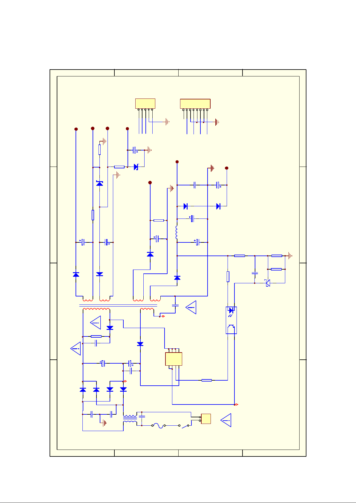
The mains power(220VAC) fed from N1 is filtered through C1, L1, C2 and L2 then rectified by D1, D2, D3 and D4
and generates an output at 300VDC. This 300VDC fed to T1 (pin2, pin4) which connects to 5L0380R(pin2), then
5L0380R will automatically generate a 50KHz square waveform, this 50KHz square waveform controls the ON/OFF
between 5L0380R pin2 and the ground. In normal condition, T1 primary (between pin2 and pin4) will create a
50KHz square waveform which is controlled by 5L0380R, this signal then fed to T1 and generates 2 different
potential voltages of 12V and 5V between pin17, pin14 and pin16, pin14 respectively. The 12VDC and 5VDC then
rectified by D7, D8, D9 and then filtered by L3, L4, L5, C9, C10 and C11. The feedback voltage is controlled by Ic3
TL431 and IC2 PC817. When the output voltage is higher than 5V, the voltage at TL431(2.5V) is compared with
R10 and send out a signal to 5L0380R, the output square waveform then will change to adjust the output voltage,
this acts as a voltage stabilizer.
15
Page 14

4.4.1 Adopt small l ens: can adopt
Thomson act lens
DV34.Hittachi .Mipseumi .
4.5
Electric
specification
4.5.1 Drive cell:adopt RF-300CA-10500 electricity machine
5.2 Electricity machine work voltage is 3V-5.9V
5.3 G
5.4 Unilate
5.5 In 5 C
Testing condition
4.6
6.1 P
6.2 e
6.3
•
6.4 Sta
6.5 Sta
eneral work voltage is 3.3V-5V
ralism(com or go) move time:<1.5S(add 5V voltage)
-10 C work current is <120mA
osition: level placed
nvironment: temperature 22+2 C
umidity 50+5%
H
Turnover storehouse voltage:5V+0.5V
ndard DVD lens testing frock
ndard DVD testing dish
16
Page 15

Page 16

DVD Service Manual
5. DESCRIPTION OF THE INTEGRATED CIRCUITS
5.1 SMPS TRANSFORMER
1. GENERAL INFORMATION
Main Voltage Operations:
Main Drop-out Voltage:
Mains STart-up Voltage:
Operating Frequency:
2. ELECTRICAL CHARACTERISTICS
2.1 STATIC CHARACTERISTICS
WINDING
Primary Inductance
1. Primary Leakage inductance (Pin 2-4) L1.5mH
2.2 WITHSTANDING VOLTAGE
The transformer shall sithstanding a voltage of 4 Kvms for 1 minute and 1 mA between
primary and seconday winding and also 2 Kvms for 1 minute and 1 mA between primary
winding with core and secondary winding with core.
PIN. NO
2-4
90Vac - 265 Vac
Max. 90 Vac
Max. 90 Vac
60 KHz
INDUCTANCE
1.5mH 10%6
DESCRIPTION
<0.50W
2.3 INSULATION RESISTANCE
The insulation resistance shall be ore than 500M between primary and seconday
windings when the applied voltage 300 Vdc for 1 minute
2.4 ELECTRICAL CHARACTERISTICS
1. Before taking measurement Pp01 will be to give 5.0Vdc on 5.0Vdc line at Minimum
setting of controls and a mains voltage 220 Vac.
2. Before taking a measurement, DVD set should be working at least 5 minutes on
Normal condition
18
Page 17

5.2 FRONT PANEL DRIVER IC FOR VIR (PT6312)
5.2.1 General Description
Operating Supply Voltage Range (TA=25 , VSS=0V)℃
DVD Service Manual
Parameter
Operating Supply Voltage range 1
Operating Supply Voltage range 2
Absolute maximum ratings (Ta=25 , VSS=0 V,0)℃
Parameter
Applied voltage 1
Applied boltage 1
Input Voltage
Power dissipation
Operating Temperature
Storage Temperature
Pin Description
Pin
VDD
OSC
VSS
SI
SO
SCK
CS
S1~S11
VEE
G1~G6
Name
Power supply pin 1
Oscillation pin
GND pin
Serial data input
Serial data output
Serial Clock input
Serial Chip select
High with standing
voltage output pin
for segment
Power supply pin 2
High with standing
voltage output pin
for grid
Pin No . I/O
14, 38 I
44
7, 43
6
5
8
9
15~25
27
37~32
Symbol
VDD
VEE
Symbol Limits
VDD
VEE
VIN
PD
TOPR
TSTG
Function
Connected to the power supply of the system
I/O
I
I
I
I
O
I
O
Connected to the oscillation capacitor
Connected to the ground of the system
Serial data input starting from MSB
Serial data output starting from MSB
Serial data read at rising edge
Serial initialization at "L", effective at "H"
Output pin for segment
Output: Pch open drain + pull - down resistance
Pull - down resistance connection for FLP driver
Output pin for grid
Output: Pch open drain + pull - down resistance
Typ. Max.Min.
5.0 5.54.5
VEE - 30 VEE - 0VEE - 32
-0.3 ~ 7.0
VDD+0.3 ~ VDD -35
-0.3 ~ VDD +0.3
850*1
-25 ~ 75
-55 ~ 125
Unit
V
V
Unit
V
V
V
MV
℃
℃
S12/G11
~S16/G7
L1~L4
K1~K4
SW1~SW4
High with standing
voltage output pin
for segment / grid
Output pin for LED
Key data input pin
General - purpose
input pin
26,
28~31
42~39
10~13
1~4
O
O
I
I
Segment / grid output selectable pin
Output: Pch open drain + pull - down resistance
Output pin for LED; output is CMOS output
Data input pin for key scanning
General - purpose input pin
Input data sent to icrocomputer in serial fromat
19
Page 18

5.3 SWPS CONTROLLER IC (VIPer22A)
DVD Service Manual
20
Page 19

DVD Service Manual
21
Page 20

DVD Service Manual
5.4 SMPS PROGRAMMABLE SHUNT REGULATOR
(FAIRCHILD TL 431)
Features
* Programmable output voltage to 36volts
* Low dynamic output impedance 0.20 typical
* Sink current capability of 1.0 to 100mA
* Equivalent full-range temperature
coefficient
of 50 ppm ℃ typical
* Temperature compensated for operation
over full rated operating temperature range
* Low output noise voltage
* Fast turn-on response
TO-92
1
1. Ref 2. Arode 3. Cathode
REFERENCE
Description
The TL 431/TL 431A are three-terminal
adjustable regulator series with a guaranteed
thermal stability over applicable temperature
ranges. The output voltage may be set to any
value between VREF (approximately 2.5
volts) and 36 volts with two external resistors.
These devices have a gypical dynamic
output impedanceof 2.0W Active oupput
circuity provides a very sharp turn-on
characteristic making these devices excel
lent replacement for zener diodes in many
applications
CATHODE
REFERENCE(R)
Absolute maximum ratings
Parameter
Cathode voltage
Cathode current Range (Continuous)
Reference Input Current Range
Power dissipation
D,Z Sffix Package
N Suffix Package
Operating Temperature Range
Storage Temperature Range
Recommended Operating conditions
Parameter
Cathode voltage
Cathode Current
2.5 Vref
Symbol
VKA
IKA
IREF
PD
TOPR
TSTG
Symbol
VKA
IKA
ANODE
CATHODE(K)
ANODE(A)
Value
37
-100 ~ +150
0.05 ~ +10
770
1000
-25 ~ +85
-65 ~ +150
Value ValueValue
- 36VREF
- 1001.0
Unit
V
MAI
MA
MW
MW
℃
℃
Unit
V
MA
22
Page 21

5.5 LINE FILTER (2 X 60mH)
ELECTRICAL DATA
Inductance: L1-2=L3-4-30mH - 15% - +20%
Resistance: R 1-2 = R 3-4 = 1.5 ohm (max)
Rated current: Irms = 0.50 A
(F= 1 Khz V= 1 Vms)
DVD Service Manual
CIRCUIT DIAGRAM
1 4
LEAKAGE INDUCTANCE
L 1-2 = L 3-4 100+/- 20%uH NOTES
2 3
23
Page 22

6. FAULT TRACING FLOW CHART
6.1 POWER SUPPLY
NO PICTURE AND FRONT PANEL
DISPLAY
CHECK POWER PCB OUTPUT
YES
DVD Service Manual
CHECK CN02
Connector
Voltages Present?
CHECK
MPEG BOARD
Voltages Present?
YES
CHECK
MPEG BOARD
NO
REPLACE
CONNECT
CABLE
OK
REPLACE
POWER PCB
NO
CHECK CON2
First pin Voltages
5V
NO
CHECK
FUSE
OK
Dp02
REPLACE Ip02,
NO
REPLACE
FUSE
24
Page 23

6.2 FRONT PANEL
NO PICTURE
DVD Service Manual
NO FRONT
PANEL DISP
LED
ON?
YES
CHECK
CN2 VOLTAGE
(5V, 3.5V, -21V)
YES
MAINBOARD
J1 PIN2: RC
DATA
PRESS ANY KEY
ON RC AND
OBSERVE
NO
NO SIGNAL
POWER
BOARD
CHECK
RANDOM
SEGMENTS
ILLUMINATED
REPLACE
IR
RECEIVER
SIGNAL
PRESS
"EJECT"
ON RC
REPLACE
MPEG2
MAINBOARD
YES
PRELACE ICF1
25
Page 24

6.3 MPEG BOARD
NO PICTURE NO AUDIO
DVD Service Manual
CHECK
CON2
VOLTAGE(5V,12V)?
YES
LOADER
RUNING?
YES
J2,J3(RGB&CVBS
RUNING?)
YES
NO
NO
NO
POWER
BOARD
CHECK
REPLACE
MPEG
BOARD
NO
INSERT A CD FOR
AUDIO TEST AND
PRESS PLAY
CHECK CN6
AUDIO OUTPUT
REPLACE
OUTPUT BOARD
YES
26
Page 25

resistence 220Ω 1/4W ±5% R6 1
resistence 470Ω 1/4W ±5% R33 1
resistence 1KΩ 1/4W ±5% CE11 1
resistence 10KΩ 1/4W ±5% R15 1
resistence 200KΩ 1/4W ±5% R22 1
resistence 120KΩ 1/2W ±5% R2 1
resistence 10KΩ 1/4W ±1% R2 2
resistence 270Ω 1W ±5% R13 1
resistence 470Ω 1W ±5% R19 1
jump φ0.6mm L=10mm R14 1
capacitance 0.1uF/50V+80%-20% C22 C24 2
capacitance 0.047uF/50V+80%-20% C23 1
capacitance 0.01uF/1KV +80%-20% C5 1
capacitance 1000pF/250V-Y1±20% CA1 1
capacitance 0.1uF/275V-X2 C1 1
capacitance 22uF/50V ±20% CE2 1
capacitance 100uF/16V ±20% CE3 1
capacitance 220uF/16V ±20% CE9 1
capacitance 220uF/35V ±20% CE6 1
capacitance 470uF/16V ±20% CE10 CE14 2
capacitance 1000uF/16V ±20% CE13 1
capacitance 33uF/400V ±20% CE4 1
inductance 17uH L6 1
diode IN4007 BR1 BR2 BR3 BR4 4
fast diode FR104 D2 D4 D5 3
fast diode FR157 D1 D7 2
diode SB360 D8 1
ziner 6.8V 1/2W D9 1
ziner 12V 1/2W D6 1
fuse clamp FUSE 2
fuse 1.6A/250V FUSE 1
filter UU10.5 L1 1
switch transformer HC EEL19 T1 1
connector panel φ4.2mm G2 1
connector VH 3.96mm CN1 SW1 2
connector XH 5P/2.54mm JP2 1
connector XH 7P/2.54mm JP202 1
optically coupled 817 IC2 1
ic TL431 IC3 1
ic VIPer22A IC1 1
 Loading...