

GENERAL DESCRIPTION
C
USTOMER PROCUREMENT SPECIFICATION
Z86C93
CMOS Z8® MULT/DIV
MICROCONTROLLER
CPS DC-4020-12
Z86C93
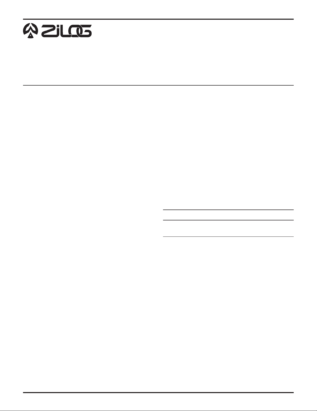
The Z86C93 is a CMOS ROMless Z8 microcontroller enhanced with a hardwired 16-bit x 16-bit multiplier,
32-bit/16-bit divider, and three 16-bit counter timers (see
Functional Block Diagram). A capture register and a fast
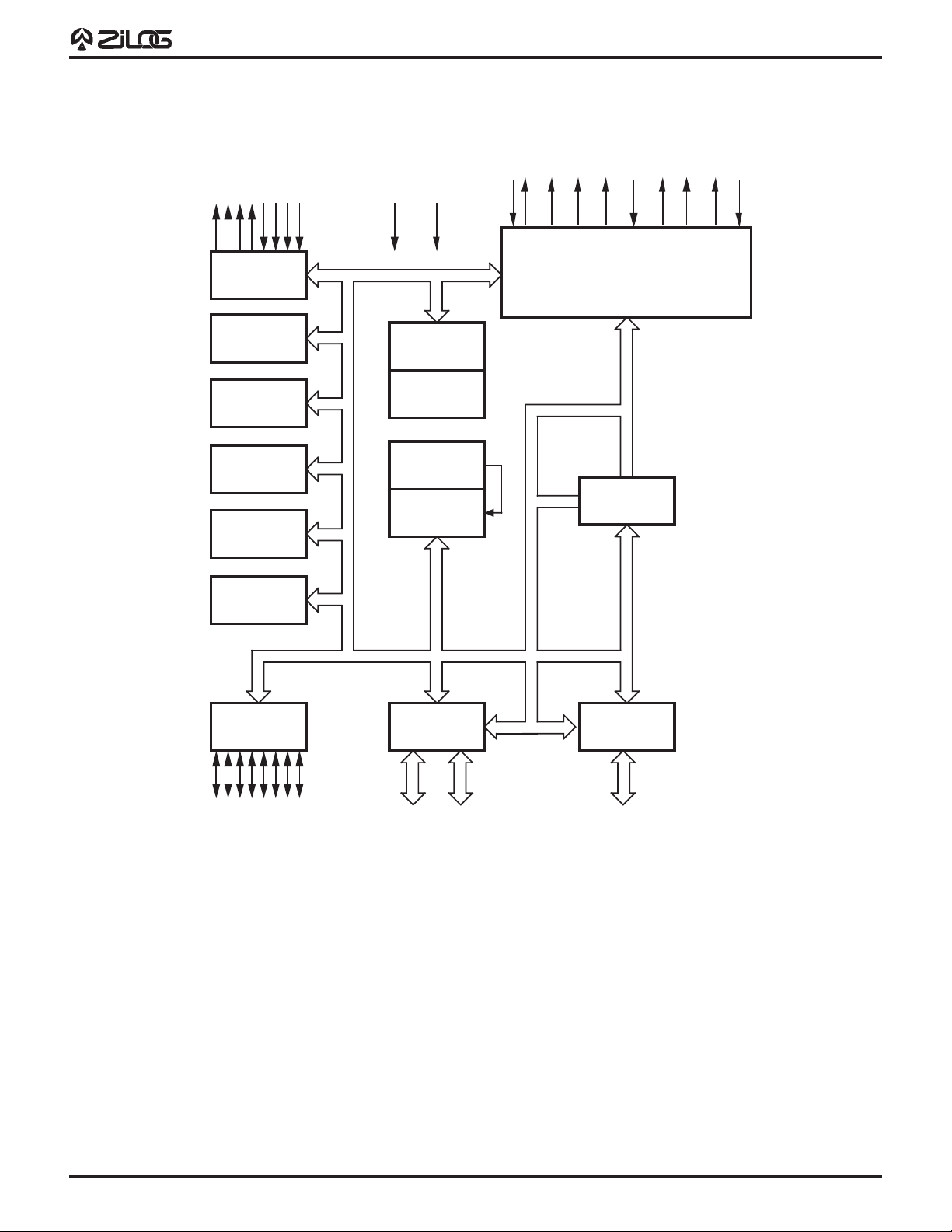
decrement mode are also provided. It is offered in 40-pin
PDIP, 44-pin PLCC, 44-pin QFP, and 48-pin VQFP packages. The Z86C93 is functionally compatible with the
Z86C91, yet it offers a more powerful mathematical capability. In the PDIP package, the Z86C93 is fully pin compatible with the Z86C91. In the PLCC package, the Z86C93 is
also pin compatible to the Z86C91, with the addition of four
signals (SCLK, /IACK, /SYNC, and /WAIT). The /WAIT
signal is only available on the 25 MHz and 33 MHz devices.
The Z86C93 provides up to 16 output address lines permitting an address space of up to 64 Kbytes of data and
program memory each. Eight address outputs (AD7-AD0)
are provided by a multiplexed, 8-bit, Address/Data bus.
The remaining 8 bits can be provided by the software
configuration of Port 0 to output address bits A15-A8.
There are 256 registers located on chip and organized as
236 general-purpose registers, 16 control and status registers, one reserved register, and up to three I/O port
registers. The register file can be divided into 16 groups of
16 working registers each. Configuration of the registers in
this manner allows the use of short format instructions; in
addition, any of the individual registers can be accessed
directly. There are an additional 17 registers implemented
in the Expanded Register File in Banks D and E. Two of the
registers may be used as general-purpose registers, while
15 registers supply the data and control functions for the
Multiply/Divide Unit and additional Counter/Timer blocks.
Notes:
All Signals with a preceding front slash, "/", are active Low, e.g.:
B//W (WORD is active Low); /B/W (BYTE is active Low, only).
Power connections follow conventional descriptions below:
Connection Circuit Device
Power V
Ground GND V
CC
V
DD
SS
DC-4020-12 (2-16-94)
1
GENERAL DESCRIPTION (Continued)
Output
Input
VCC GND
XTAL
/AS
/DS
R//W
/RESET
SCLK
IACK
/WAIT
/SYNC
(25 MHz & 33 MHz
CPS DC-4020-12
Z86C93
Devices Only.)
Port 3
UART
Three 16-Bit
Counter/Timers
32 ÷ 16
Divider
16 x 16
Multiplier
Interrupt
Control
ALU
FLAGS
Register
Pointer
Register File
256 x 8-Bit
Machine Timing, Emulation
and Instruction Control
Program
Counter
Port 2
I/O
(Bit Programmable)
Port 0
44
Address or I/O
(Nibble Programmable)
Functional Block Diagram
Port 1
8
Address/Data
2

T
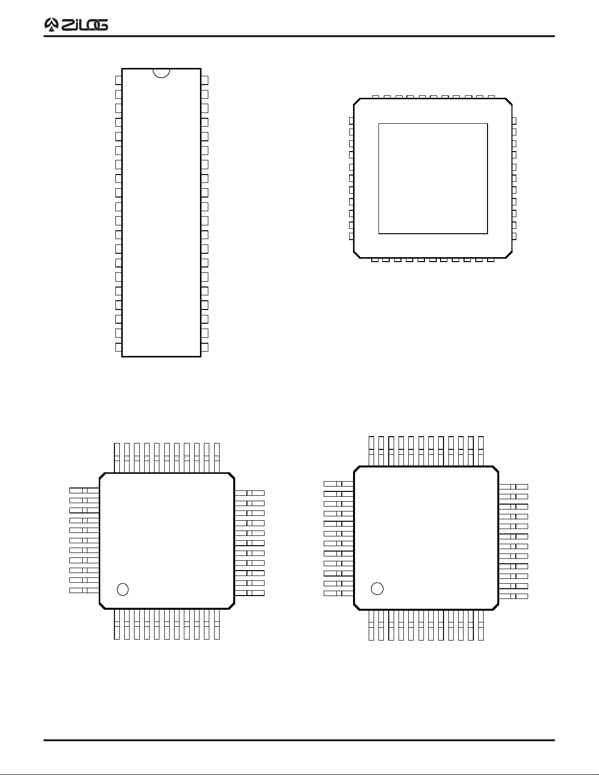
PIN CONFIGURATION
CPS DC-4020-12
Z86C93
VCC
XTAL2
XTAL1
P37
P30
/RESE
R//W
/DS
/AS
P35
GND
P32
P00
P01
P02
P03
P04 P13
P05
P06
P07
1
2
3
4
5
6
7
8
9
10
11
12
13
15
16
17
18
19
20
Z86C93
DIP
40
39
38
37
36
35
34
33
32
31
30
29
28
2714
26
25
24
23
22
21
P36
P31
P27
P26
P25
P24
P23
P22
P21
P20
P33
P34
P17
P16
P15
P14
P12
P11
P10
/RESET
R//W
/DS
/AS
P35
GND
P32
P00
P01
P02
IACK
XTAL2
XTAL1
Z86C93
MCU
P07
P06
+5V
P10
P11
P12
P13
P37
P30
SCLK
6543214443424140
7
8
9
10
11
12
13
14
15
16
17
18 19 20 21 22 23 24 25 26 27 28
P05
P04
P03
P27
P31
P36
44-Pin PLCC Package
(20 MHz)
P26
P14
P25
39
38
37
36
35
34
33
32
31
30
29
/SYNC
NC
P24
P23
P22
P21
P20
P33
P34
P17
P16
P15
P25
P26
P27
P31
P36
+5V
XTAL2
XTAL1
P37
P30
SCLK
40-Pin DIP Package
(20 MHz)
NC
P24
P23
P22
P21
P20
33 32 31 30 29 28 27 26 25 24 23
34
35
36
37
38
39
40
41
42
43
44
1234567891011
/RESET
R//W
/DS
Z86C93
MCU
/AS
P35
GND
P33
P32
P34
P00
P17
P01
P16
P02
P15
22
21
20
19
18
17
16
15
14
13
12
IACK
/SYNC
P14
P13
P12
P11
P10
P07
P06
P05
P04
P03
P25
P26
P27
P31
P36
NC
+5V
XTAL2
XTAL1
P37
P30
SCLK
NC
P24
P23
P22
P21
P20
P33
P34
36 35 34 33 32 31 30 29 28 27 26
37
38
39
40
41
42
43
44
45
46
47
48
23456789101112
1
NC
R//W
/RESET
Z86C93
/AS
/DS
MCU
P35
GND
P32
P17
P00
P16
P01
P15
P02
25
NC
24
23
22
21
20
19
18
17
16
15
14
13
IACK
/SYNC
P14
P13
P12
P11
P10
P07
NC
P06
P05
P04
P03
44-Pin QFP Package
(20 MHz)
48-Pin VQFP Package
(20 MHz)
3
PIN CONFIGURATIONS (Continued)
T
/SYNC
P14
P13
P12
P11
P10
P07
P06
P05
P04
P03
P25
P26
P27
P31
P36
+5V
XTAL2
XTAL1
P37
P30
SCLK
CPS DC-4020-12
Z86C93
VCC
XTAL2
XTAL1
P37
P30
/RESE
R//W
/DS
/AS
P35
GND
P32
P00
P01
P02
P03
P04 P13
P05
P06
P07
1
2
3
4
5
6
7
8
9
10
11
12
13
15
16
17
18
19
20
Z86C93
DIP
40
39
38
37
36
35
34
33
32
31
30
29
28
2714
26
25
24
23
22
21
P36
P31
P27
P26
P25
P24
P23
P22
P21
P20
P33
P34
P17
P16
P15
P14
P12
P11
P10
/RESET
R//W
/DS
/AS
P35
GND
P32
P00
P01
P02
IACK
6543214443424140
7
8
9
10
11
12
13
14
15
16
17
18 19 20 21 22 23 24 25 26 27 28
Z86C93
MCU
44-Pin PLCC Package
(25 MHz and 33 MHz)
39
/WAIT
38
P24
37
P23
36
P22
35
P21
34
P20
33
P33
32
P34
31
P17
30
P16
29
P15
P25
P26
P27
P31
P36
+5V
XTAL2
XTAL1
P37
P30
SCLK
40-Pin DIP Package
(25 MHz and 33 MHz)
/WAIT
P24
P23
P22
P21
P20
P33
33 32 31 30 29 28 27 26 25 24 23
34
35
36
37
38
39
40
41
42
43
44
1234567891011
/RESET
R//W
/DS
Z86C93
MCU
/AS
P35
GND
P32
P34
P00
P17
P01
P16
P02
P15
22
21
20
19
18
17
16
15
14
13
12
IACK
/SYNC
P14
P13
P12
P11
P10
P07
P06
P05
P04
P03
P25
P26
P27
P31
P36
NC
+5V
XTAL2
XTAL1
P37
P30
SCLK
/WAIT
P24
P23
P22
P21
P20
P33
P34
36 35 34 33 32 31 30 29 28 27 26
37
38
39
40
41
42
43
44
45
46
47
48
23456789101112
1
NC
R//W
/RESET
Z86C93
/AS
/DS
MCU
P35
GND
P32
P17
P00
P16
P01
P15
P02
25
NC
24
23
22
21
20
19
18
17
16
15
14
13
IACK
/SYNC
P14
P13
P12
P11
P10
P07
NC
P06
P05
P04
P03
44-Pin QFP Package
(25 MHz and 33 MHz)
4
48-Pin VQFP Package
(25 MHz and 33 MHz)

ABSOLUTE MAXIMUM RATINGS
CPS DC-4020-12
Z86C93
Symbol Description Min Max Units
V
CC
T
STG
T
A
Supply Voltage* –0.3 +7.0 V
Storage Temp –65 +150 C
Oper Ambient Temp † † C
* Voltages on all pins with respect to GND.
† See Ordering Information
STANDARD TEST CONDITIONS
The characteristics listed below apply for standard test
conditions as noted. All voltages are referenced to GND.
Positive current flows into the referenced pin (Test Load
Diagram).
Stress greater than those listed under Absolute Maximum
Ratings may cause permanent damage to the device. This
is a stress rating only; operation of the device at any
condition above those indicated in the operational sections of these specifications is not implied. Exposure to
absolute maximum rating conditions for an extended period may affect device reliability.
I
OL
DUT
Device Under Test
V Commutation
50 pf
I
OH
Test Load Diagram
5

DC ELECTRICAL CHARACTERISTICS
VCC = 3.3V ± 10%
CPS DC-4020-12
Z86C93
T
= 0°C to +70°C Typical
A
Sym Parameter Min Max at 25°C Units Conditions
Max Input Voltage 7 V I
V
CH
V
CL
V
IH
V
IL
V
OH
V
OH
V
OL
V
RH
V
Rl
I
IL
I
OL
I
IR
I
CC
I
CC1
I
CC2
I
AL
Note:
[1] All inputs driven to 0V, or Vcc and outputs floating.
Clock Input High Voltage 0.8 V
CC
V
CC
Clock Input Low Voltage –0.03 0.1xV
Input High Voltage 0.7xV
CC
V
CC
Input Low Voltage –0.3 0.1xV
Output High Voltge 1.8 V IOH= –1.0 mA
Output High Voltage VCC –100mV V I
Output Low Voltage 0.4 V IOL = +1.0 mA
Reset Input High Voltage 0.8xV
CC
V
CC
Reset Input Low Voltage -0.03 0.1xV
Input Leakage –2 2 µA Test at 0V, V
Output Leakage –2 2 µA Test at 0V, V
Reset Input Current –180 µAV
Supply Current 30 20 mA @ 25 MHz [1]
Standby Current (HALT Mode) 12 8 mA HALT Mode V
Standby Current (HALT Mode) 8 1 µA STOP Mode V
Auto Latch Current –10 10 5 µA
V Driven by External Clock Generator
CC
V Driven by External Clock Generator
V
CC
V
V
CC
V
250 µA
IN
= –100 µA
OH
= 0V
RL
CC
CC
= OV, VCC @ 25 MHz [1]
IN
= OV, VCC [1]
IN
6

DC ELECTRICAL CHARACTERISTICS
VCC = 5.0V ± 10%
CPS DC-4020-12
Z86C93
T
= 0°C to +70°C Typical
A
Sym Parameter Min Max at 25°C Units Conditions
Max Input Voltage 7 V I
V
CH
V
CL
V
IH
V
IH
V
IL
V
OH
V
OH
V
OL
V
RH
V
Rl
I
IL
I
OL
I
IR
I
CC
Clock Input High Voltage 3.8 V
CC
V Driven by External Clock Generator
Clock Input Low Voltage –0.03 0.8 V Driven by External Clock Generator
Input High Voltage (P0,P1,P2) 2.0 V
Input High Voltage (P3) 2.2 V
CC
CC
V
V
Input Low Voltage –0.3 0.8 V
Output High Voltge 2.4 V IOH= –2.0 mA
Output High Voltage VCC –100mV V I
Output Low Voltage 0.4 V IOL = +5 mA
Reset Input High Voltage 3.8 V
CC
V
Reset Input Low Voltage –0.03 0.8 V
Input Leakage –2 2 µA Test at 0V, V
Output Leakage –2 2 µA Test at 0V, V
Reset Input Current –180 µAV
Supply Current 55 35 mA @ 33 MHz [1]
250 µA
IN
= –100 µA
OH
= 0V
RL
40 25 mA @ 25 MHz [1]
30 20 mA @ 20 MHz [1]
I
CC1
Standby Current (HALT Mode) 20 15 mA HALT Mode V
15 9 mA HALT Mode VIN = OV, VCC @ 25 MHz [1]
12 7 mA HALT Mode VIN = OV, VCC @ 20 MHz [1]
I
CC2
I
AL
Standby Current 10 1 µA STOP Mode V
Auto Latch Current –16 16 5 µA
CC
CC
= OV, VCC @ 33 MHz [1]
IN
= OV, VCC [1]
IN
Note:
[1] All inputs driven to 0V, or Vcc and outputs floating.
7
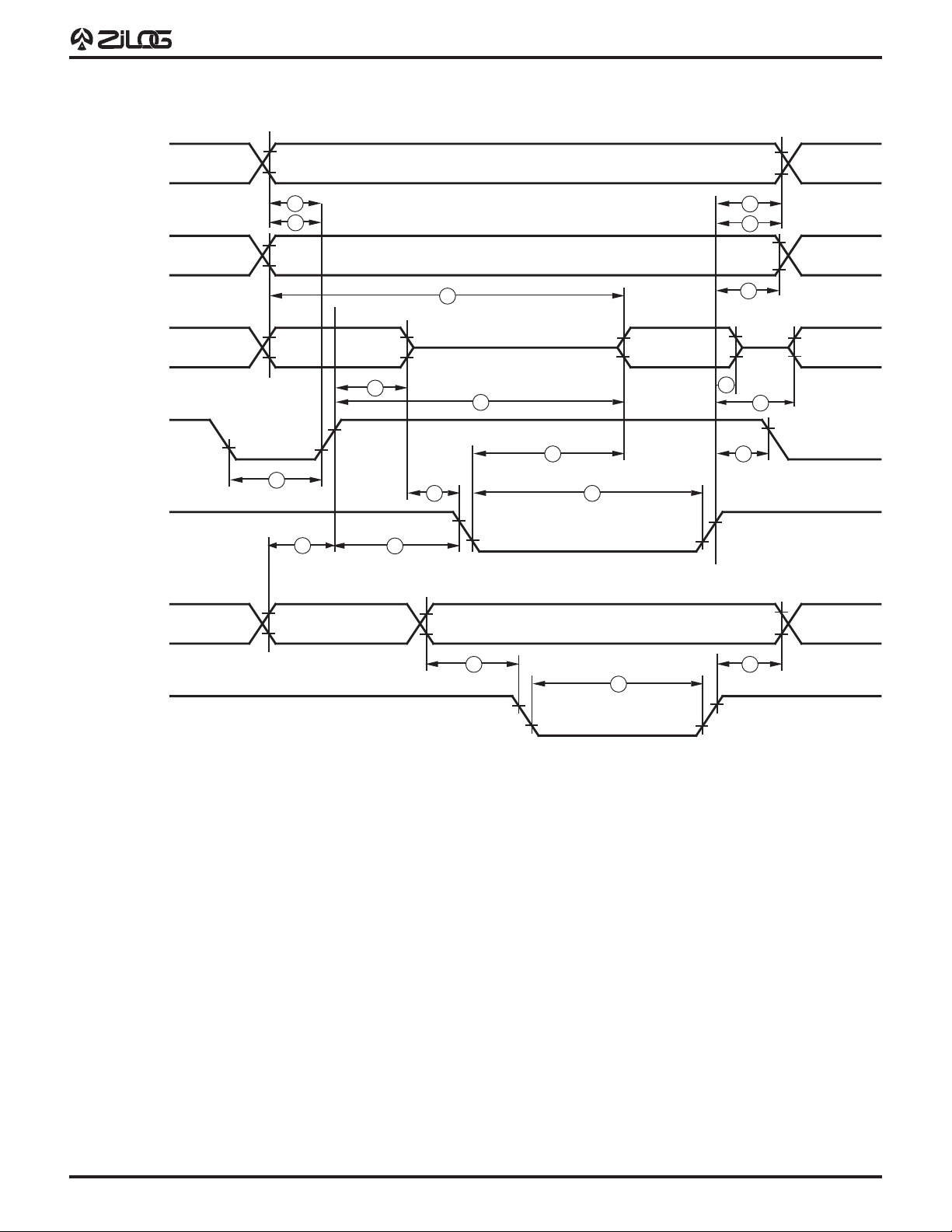
AC CHARACTERISTICS
External Memory Read/Write Timing Diagram
R/W, /DM
CPS DC-4020-12
Z86C93
Port 0
Port 1
/AS
/DS
(Read)
Port1
19
12
20
13
A8 - A15
16
A0 - A7
2
4
1
17
A0 - A7
3
8 11
5
6
D0 - D7 OUT
D0 - D7 IN
21
A0 - A7
9
10
A0-A7
/DS
(Write)
14
External Memory Read/Write Timing
15
7
8

CPS DC-4020-12
AC CHARACTERISTICS
External I/O or Memory Read and Write; DSR/DSW; WAIT Timing Table
T
= 0°C to +70°C
33 MHz 25 MHz 20 MHz
No Sym Parameter Min Max Min Max Min Max Units
1 TdA(AS) Address Valid To /AS Rise Delay 15 22 26 ns
2 ThAS(A) /AS Rise To Address Hold Time 20 25 28 ns
3 TdAS(DI) /AS Rise To Data In Req’d Valid Delay 96 130 160 ns
4 TwAS /AS Low Width 15 28 36 ns
5 TdAZ(DSR) Address Float To /DS Fall (Read) 0 0 0 ns
6 TwDSR /DS (Read) Low Width 65 100 130 ns
7 TwDSW /DS (Write) Low Width 40 65 75 ns
8 TdDSR(DI) /DS Fall (Read) To Data in Req'd Valid Delay 55 85 100 ns
9 ThDSR(DI) /DS Rise (Read) to Data In Hold Time 0 0 0 ns
10 TdDS(A) /DS Rise To Address Active Delay 25 40 48 ns
11 TdDS(AS) /DS Rise To /AS Delay 16 30 36 ns
12 TdR/W(AS) R/W Valid To /AS Rise Delay 12 26 32 ns
13 TdDS(R/W) /DS Rise To R/W Not Valid Delay 12 30 36 ns
14 TdDO(DSW) Data Out To /DS Fall (Write) Delay 12 34 40 ns
15 ThDSW(DO) /DS Rise (Write) To Data Out Hold Time 12 34 40 ns
16 TdA(DI) Address Valid To Data In Req’d Valid Delay 115 160 200 ns
A
Z86C93
17 TdAS(DSR) /AS Rise To /DS Fall (Read) Delay 30 40 48 ns
19 TdDM(AS) /DM Valid To /AS Rise Delay 15 22 26 ns
20 TdDS(DM) /DS Rise To /DM Valid Delay 15 34* ns
21 ThDS(A) /DS Rise To Address Valid Hold Time 35 ns
22 TdXT(SCR) XTAL Falling to SCLK Rising** 35 ns
23 TdXT(SCF) XTAL Falling to SCLK Falling** 45 ns
24 TdXT(DSRF) XTAL Falling to/DS Read Falling** 35 ns
25 TdXT(DSRR) XTAL Falling to /DS Read Rising** 35 ns
26 TdXT(DSWF) XTAL Falling to /DS Write Falling** 45 ns
27 TdXT(DSWF) XTAL Falling to /DS Write Rising** 35 ns
28 TsW(XT) Wait Set-up Time 5 10* ns
29 ThW(XT) Wait Hold Time 15 15* ns
30 TwW Wait Width (One Wait Time) 20 25* ns
Notes:
When using extended memory timing add 2 TpC.
Timing numbers given are for minimum TpC.
* Typical value to be characterized (25 MHz).
** External clock drive.
9

XTAL1
(External Clock Drive)
SCLK
CPS DC-4020-12
Z86C93
2322
/DS
DSR
(READ)
/DS
DSW
(Write)
XTAL1
24
26
XTAL/SCLK To DSR and DSW Timing
T1 T2 TW TW TW T3 T1
25
27
10
SCLK
/AS
/DS
/WAIT
32
30
31
XTAL/SCLK To WAIT Timing
(25 MHz and 33 MHz Devices Only)

AC CHARACTERISTICS
Additional Timing Diagram
CPS DC-4020-12
Z86C93
Clock
T IN
IRQ N
AC CHARACTERISTICS
Additional Timing Table
7 7
8
1
2 2 3
4
5
6
9
Additional Timing
3
T
= 0°C to +70°C
A
33 MHz 25 MHz 20 MHz
No Symbol Parameter Min Max Min Max Min Max Units Notes
1 TpC Input Clock Period 30 1000 42 1000 50 1000 ns [1]
2 TrC,TfC Clock Imput Rise & Fall Times 5 10 10 ns [1]
3 TwC Input Clock Width 10 11 15 ns [1]
4 TwTinL Timer Input Low Width 75 75 75 ns [2]
5 TwTinH Timer Input High Width 3 TpC 3 TpC 3 TpC [2]
6 TpTin Timer Input Period 8 TpC 8 TpC 8 TpC [2]
7 TrTin,TfTin Timer Input Rise & Fall Times 100 100 100 ns [2]
8A TwIL Interrupt Request Input Low Times 70 70 70 ns [2,4]
8B TwIL Interrupt Request Input Low Times 5 TpC 5 TpC 5 TpC [2,5]
9 TwIH Interrupt Request Input High Times 3 TpC 3 TpC 3 TpC [2,3]
Notes:
[1] Clock timing references use 3.8V for a logic 1 and 0.8V for a logic 0.
[2] Timing references use 2.0V for a logic 1 and 0.8V for a logic 0.
[3] Interrupt references request through Port 3.
[4] Interrupt request via Port 3 (P33-P31)`.
[5] Interrupt request via Port 30.
11
AC CHARACTERISTICS
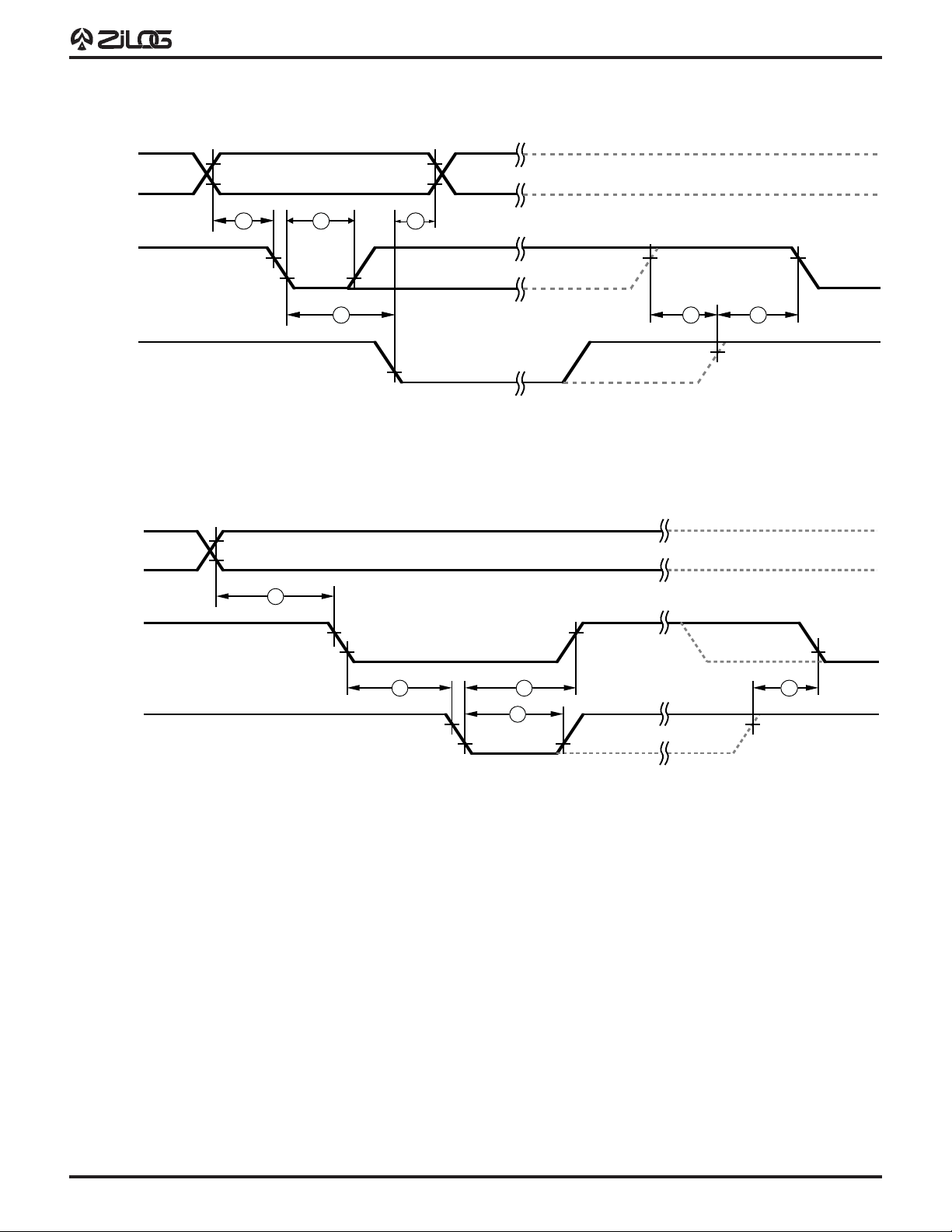
Handshake Timing Diagrams
CPS DC-4020-12
Z86C93
Data In
/DAV
(Input)
RDY
(Output)
Data Out
Data In Valid
1 3
7
Next Data In Valid
2
Delayed DAV
4 5 6
Delayed RDY
Input Handshake Timing
Data Out Valid
Next Data Out Valid
/DAV
(Output)
RDY
(Input)
8 9
10
Output Handshake Timing
Delayed DAV
11
Delayed RDY
12

CPS DC-4020-12
Z86C93
AC CHARACTERISTICS
Handshake Timing Table
TA = 0°C to +70°C Data
No Symbol Parameter Min Max Units Direction
1 TsDI(DAV) Data In Setup Time to /DAV 0 ns In
2 ThDI(DAV) RDY to Data In Hold Time 0 ns In
3 TwDAV /DAV Width 40 ns In
4 TdDAVIf(RDYf) /DAV to RDY Delay 70 ns In
5 TdDAVIr(RDYr) DAV Rise to RDY Wait Time 40 ns In
6 TdRDYOr(DAVIf) RDY Rise to DAV Delay 0 ns In
7 TdD0(DAV) Data Out to DAV Delay TpC ns Out
8 TdDAV0f(RDYIf) /DAV to RDY Delay 0 ns Out
9 TdRDYIf(DAVOr) RDY to /DAV Rise Delay 70 ns Out
10 TwRDY RDY Width 40 ns Out
11 TdRDYIr(DAVOf) RDY Rise to DAV Wait Time 40 ns Out
© 1994 by Zilog, Inc. All rights reserved. No part of this document
may be copied or reproduced in any form or by any means
without the prior written consent of Zilog, Inc. The information in
this document is subject to change without notice. Devices sold
by Zilog, Inc. are covered by warranty and patent indemnification
provisions appearing in Zilog, Inc. Terms and Conditions of Sale
only. Zilog, Inc. makes no warranty, express, statutory, implied or
by description, regarding the information set forth herein or
regarding the freedom of the described devices from intellectual
property infringement. Zilog, Inc. makes no warranty of merchantability or fitness for any purpose. Zilog, Inc. shall not be
responsible for any errors that may appear in this document.
Zilog, Inc. makes no commitment to update or keep current the
information contained in this document.
Zilog’s products are not authorized for use as critical components in life support devices or systems unless a specific written
agreement pertaining to such intended use is executed between
the customer and Zilog prior to use. Life support devices or
systems are those which are intended for surgical implantation
into the body, or which sustains life whose failure to perform,
when properly used in accordance with instructions for use
provided in the labeling, can be reasonably expected to result in
significant injury to the user.
Zilog, Inc. 210 East Hacienda Ave.
Campbell, CA 95008-6600
Telephone (408) 370-8000
Telex 910-338-7621
FAX 408 370-8056
13
 Loading...