

FEATURES
Z86C15
CP96KEY0603
CUSTOMER PROCUREMENT SPECIFICATION
Z86C15
CMOS Z8® 8-BIT MCU
KEYBOARD CONTROLLER
ROM RAM* I/O Speed Pin Count /
(Kbytes) (Bytes) Lines (MHz) Package
4 2 36 3 2 5 40 DIP
44 PLCC
44 QFP
* General-Purpose
n 4.5- to 5.5-Volt Operating Range
n 0°C to 70°C Operating Temperature Range
n Expanded Register File
n Low-Power Consumption: 30 mW @ 5 MHz Typical
GENERAL DESCRIPTION
The Z86C15 Keyboard Controller is a full-featured member of the Z8® microcontroller family offering a unique
register-to-register architecture that avoids accumulator
bottlenecks and is more code efficient than RISC
processors.
For applications demanding powerful I/O capabilities, the
Z86C15 provides 32 pins dedicated to input and output.
These lines are grouped into four ports, each port consisting of eight lines, and are configurable under software
control to provide timing, status signals, and serial or
parallel I/O ports.
n Six Vectored, Priority Interrupts from
Six Different Sources
n Two Programmable 8-Bit Counter/Timers,
Each with 6-Bit Programmable Prescaler
n Power-On Reset (POR) Timer, Hardware Watch-Dog
Timer (WDT)
n Digital Inputs CMOS Levels with
Internal Pull-Up Resistors
n Four Direct Connect LED Drive Ports
n On-Chip RC Oscillator, 4 MHz to 5 MHz
The Z86C15 achieves low-EMI by means of several modifications in the output drivers and clock circuitry of the
device.
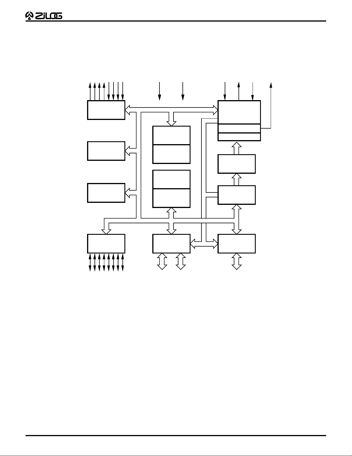
By means of an expanded register file, the designer has
access to three additional system control registers that
provide extra peripheral devices, I/O ports, and register
addresses (see Functional Block Diagram).
Notes:
All Signals with a preceding front slash, "/", are active Low, e.g.,
B//W (WORD is active Low); /B/W (BYTE is active Low, only).
Two on-chip counter/timers, with a large number of userselectable modes, are available to relieve the system of
administering real-time tasks, such as counting/timing and
I/O datacommunications.
Six different internal or external interrupt sources are
maskable and prioritized so a vectored address is provided for efficient interrupt subroutine handling and
multitasking functions.
CP96KEY0603 (3/96)
Power connections follow conventional descriptions below:
Connection Circuit Device
Power V
Ground GND V
CC
V
DD
SS
1
GENERAL DESCRIPTION (Continued)
Z86C15
CP96KEY0603
Output Input
Port 3
Counter/
Timers (2)
Interrupt
Control
Port 2
Vcc GND
ALU
Flags
Register
Pointer
Register File
258 x 8-Bit
Port 0 Port 1
RCIN
CLKOUT
Machine
Timing & Inst.
Control
WDT
POR
Program
Memory
Program
Counter
/RESET
/WDTOUT
I/O
(Bit Programmable)
44 8
I/O
(Nibble Programmable)
(Byte Programmable)
Z86C15 Functional Block Diagram
I/O
2
PIN IDENTIFICATION
/
is
Z86C15
CP96KEY0603
VCC
CLKOUT
RCIN
P37
P30
/RESET
AGND
*NC
WDTOUT
P35
GND
P32
P00
P01
P02
P03
P04
P05
P06
P07
1
2
3
4
5
6
7
8
9
10
11
12
13
14
15
16
17
18
19
20
Z86C15
DIP
40
39
38
37
36
35
34
33
32
31
30
29
28
27
26
25
24
23
22
21
P36
P31
P27
P26
P25
P24
P23
P22
P21
P20
P33
P34
P17
P16
P15
P14
P13
P12
P11
P10
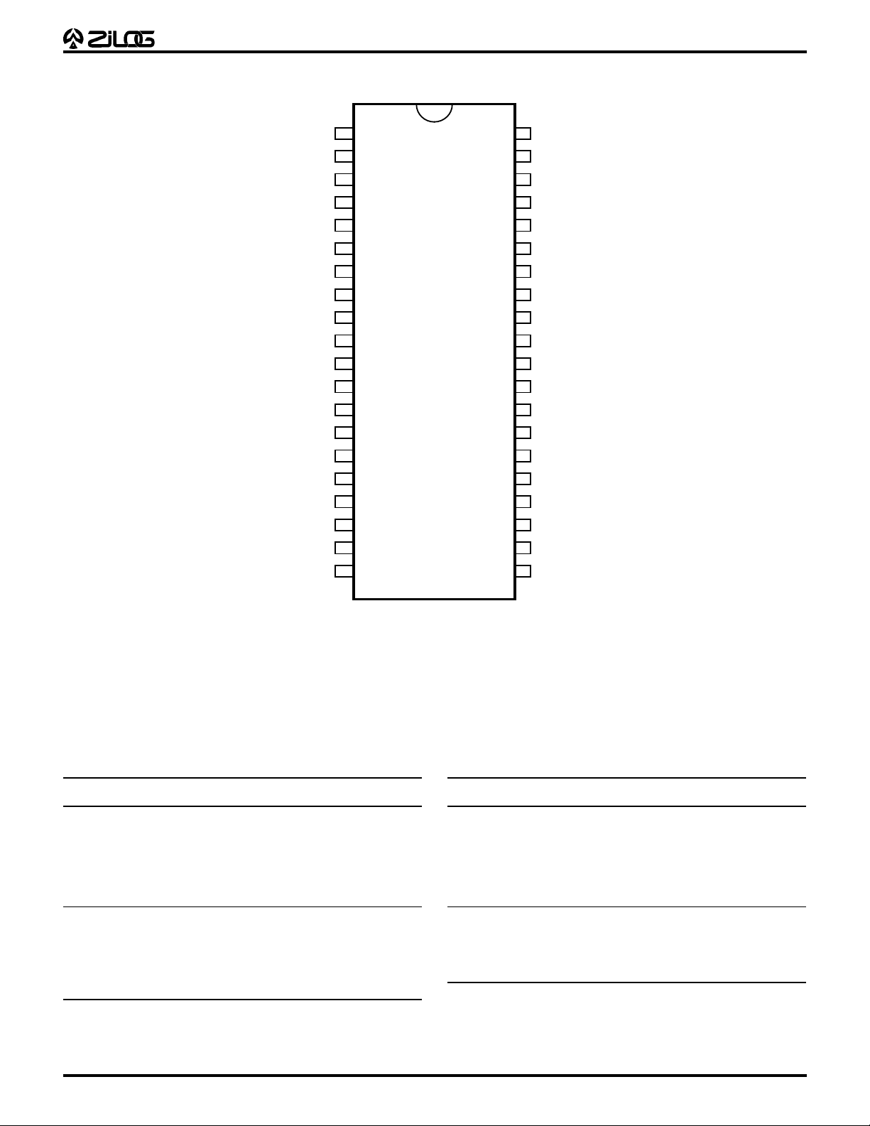
*Note: Pin 8 is connected to the chip, although it
used only for testing. This pin must float.
40-Pin DIP Pin Configuration
40-Pin DIP Pin Identification
Pin # Symbol Function Direction
1VCCPower Supply Input
2 CLKOUT Z8 System Clock Output
3 RCIN RC Oscillator Clock Input
4 P 37 Port 3, Pin 7 Output
5 P 30 Port 3, Pin 0 Input
6 /RESET Reset Input
7 AGND Analog Ground
*8 NC Not Connected
9 /WDTOUT Watch-Dog Timer Output
1 0 P 35 Port 3, Pin 5 Output
Pin # Symbol Function Direction
11 GND Ground
1 2 P 32 Port 3, Pin 2 Input
13-20 P00-P07 Port 0, Pins 0,1,2,3,4,5,6,7 In/Output
21-28 P10-P17 Port 1, Pins 0,1,2,3,4,5,6,7 In/Output
2 9 P 34 Port 3, Pin 4 Output
3 0 P 33 Port 3, Pin 3 Input
31-38 P20-P27 Port 2, Pins 0,1,2,3,4,5,6,7 In/Output
3 9 P 31 Port 3, Pin 1 Input
4 0 P 36 Port 3, Pin 6 Output
3

PIN IDENTIFICATION (Continued)
/RESET
AGND
*N/C
/WDTOUT
P35
GND
P32
P00
P01
P02
N/C
7
8
9
10
11
12
13
14
15
16
17
N/C
P30
P37
RCIN
6543214443424140
VCC
CLKOUT
P36
P31
P27
P26
P25
Z86C15
PLCC
39
38
37
36
35
34
33
32
31
30
29
Z86C15
CP96KEY0603
N/C
P24
P23
P22
P21
P20
P33
P34
P17
P16
P15
18 19 20 21 22 23 24 25 26 27 28
P03
P04
P05
P06
*Note: Pin 9 is connected to the chip, although it is used
only for testing. This pin must float.
44-Pin PLCC Pin Assignments
44-Pin PLCC Pin Identification
Pin # Symbol Function Direction
1VCCPower Supply Input
2 CLKOUT Z8 System Clock Output
3 RCIN RC Oscillator Clock Input
4 P 37 Port 3, Pin 7 Output
5 P 30 Port 3, Pin 0 Input
6 N/C Not Connected
7 /RESET Reset Input
8 AGND Analog Ground
P07
P10
P11
P12
P13
P14
N/C
Pin # Symbol Function Direction
14-16 P00-P02 Port 0, Pins 0, 1, 2 In/Output
17 N/C Not Connected
18-22 P03-P07 Port 0, Pins 3, 4, 5, 6, 7 In/Output
23-27 P10-P14 Port 1, Pins 0, 1, 2, 3, 4 In/Output
28 N/C Not Connected
29-31 P15-P17 Port 1, Pins 5, 6, 7 In/Output
3 2 P3 4 Port 3, Pin 4 Output
3 3 P3 3 Port 3, Pin 3 Input
*9 N/C Not Connected
10 /WDTOUT Watch-Dog Timer Output
1 1 P 35 Port 3, Pin 5 Output
12 GND Ground
1 3 P 32 Port 3, Pin 2 Input
4
34-38 P20-P24 Port 2, Pins 0, 1, 2, 3, 4 In/Output
39 N/C Not Connected
40-42 P25-P27 Port 2, Pins 5, 6, 7 In/Output
4 3 P3 1 Port 3, Pin 1 Input
4 4 P3 6 Port 3, Pin 6 Output

/RESET
AGND
*N/C
/WDTOUT
P35
GND
P32
P00
P01
P02
N/C
RCIN
CLKOUT
P30
P37
N/C
44 43 42 41 40 39 38 37 36 35 34
1
2
3
4
5
6
7
8
9
10
11
13 14 15 16 17 18 19 20 21 22
12
VCC
Z86C15
QFP
P36
P31
P27
P26
P25
33
32
31
30
29
28
27
26
25
24
23
Z86C15
CP96KEY0603
N/C
P24
P23
P22
P21
P20
P33
P34
P17
P16
P15
P03
P04
P05
P06
*Note: Pin 3 is connected to the chip, although it is used
only for testing. This pin must float.
44-Pin QFP Pin Assignments
44-Pin QFP Pin Identification
Pin # Symbol Function Direction
1 /RESET Reset Input
2 AGND Analog Ground
*3 N/C Not Connected
4 /WDTOUT Watch-Dog Timer Output
5 P3 5 Port 3, Pin 5 Output
6 GND Ground
7 P3 2 Port 3, Pin 2 Input
8-10 P00-P02 Port 0, Pins 0, 1, 2 In/Output
11 N/C Not Connected Input
12-16 P03-P07 Port 0, Pins 3,4,5,6,7 In/Output
17-21 P10-P14 Port 1, Pins 0,1,2,3,4 In/Output
22 N/C Not Connected
23-25 P15-P17 Port 1, Pins 5, 6,7 In/Output
P07
P10
P12
P13
P14
P11
N/C
Pin # Symbol Function Direction
2 6 P 3 4 Port 3, Pin 4 Output
2 7 P 3 3 Port 3, Pin 3 Input
28-32 P20-P24 Port 2, Pins 0, 1, 2, 3, 4 In/Output
33 N/C Not Connected
34-36 P25-P27 Port 2, Pins 5, 6, 7 In/Output
3 7 P 3 1 Port 3, Pin 1 Input
38 P36 Port 36 Output
39 V
CC
Power Supply
40 CLKOUT Z8 System Clock Output
41 RCIN RC Oscillator Clock Input
4 2 P 3 7 Port 3, Pin 7 Output
4 3 P 3 0 Port 3, Pin 0 Input
44 N/C Not Connected
5

ABSOLUTE MAXIMUM RATINGS
Z86C15
CP96KEY0603
Symbol Description Min Max Units
V
CC
T
STG
T
A
Notes:
* Voltage on all pins with respect to GND.
Supply Voltage* –0.3 +7.0 V
Storage Temp –65 +150 °C
Oper Ambient Temp 0 +105 °C
STANDARD TEST CONDITIONS
Standard Test Conditions. The characteristics listed
here apply for standard test conditions as noted. All
voltages are referenced to GND. Positive current flows into
the referenced pin (Test Load).
Stresses greater than those listed under Absolute Maximum Ratings may cause permanent damage to the device. This is a stress rating only; operation of the device at
any condition above those indicated in the operational
sections of these specifications is not implied. Exposure to
absolute maximum rating conditions for extended periods
may affect device reliability.
From Output
Under Test
150 pF
Test Load Diagram
CAPACITANCE
T
= 25°C; VCC = GND = 0V; f = 1.0 MHz; unmeasured pins returned to GND.
A
Parameter Max
Input Capacitance 12 pF
Output Capacitance 12 pF
I/O Capacitance 12 pF
FREQUENCY
Frequency 4 MHz – 5 MHz
Tolerance ±10%
Frequency tolerance limit only applies to the packaged device and not die or wafer.
6

DC CHARACTERISTICS (Z86C15)
VCC = 5.0V ±10% @ 0°C to +70°C
Typical
Sym Parameter Min Max @ 25°C Unit Condition
Z86C15
CP96KEY0603
V
V
V
V
V
V
V
V
V
V
I
OL
I
IL
I
OL
I
CC
Clock Input High Voltage 0.7 V
CH
Clock Input Low Voltage GND –0.3 0.2 V
CL
Input High Voltage 0.7 V
IH
Input Low Voltage GND –0.3 0.2V
IL
Reset Input High Voltage 0.8 V
RH
Reset Input Low Voltage GND –0.3 0.2 V
RL
Output High Voltage VCC –0.4 3 .1 V IOH = –2.0 mA
OH
Output High Voltage VCC 0.6 V IOH = –2.0 mA (See note [1] below.)
OH
Output Low Voltage 0.8 V IOL = 4 mA (See note [1] below.)
OL
Output Low Voltage .4 V IOL= 4 mA
OL
VCC to +0.3V 2.5 V Driven by External Clock Generator
CC
V
CC
CC
+ 0.3 2 .5 V
CC
CC
V
CC
1.5 V Driven by External Clock Generator
CC
1.5 V
2.1 V
1.7 V
CC
Output Low 8 20 mA VOL= V
Input Leakage –1 1 <1 µAVIN = 0V, 5.25V (See note [2] beow.)
Output Leakage –1 1 <1 µAVIN = 0V, 5.25V
VCC Supply Current 12 6 mA @ 5.0 MHz
POR Power On Reset 84 196 140 m s
I
CC1
I
CC2
R
R
Standby Current 4 2.0 mA HALT mode VIN = 0V, VCC @ 5 MHz
Standby Current 20 µA STOP mode VIN = 0V
Pull Up Resistor 6.76 14.04 10.4 Kohm
P
Pull Up Resistor
P
(P26-P27) 1.8 3 2.4 Kohm
R
Pull Up Resistor
P
(Reset) 40 80 60 Kohm
–2.2 V (See note [1] below.)
CC
Note:
[1] Ports P37-P34. These may be used for LEDs or as general-purpose
outputs requiring high sink current.
[2] Input pin without pull-up resistor.
7

Z86C15
CP96KEY0603
AC ELECTRICAL CHARACTERISTICS (Z86C15)
Additional Timing Table
TA = 0°C to +70°C
V
CC
No Symbol Parameter Note [4] Min Max Units Notes
1 TpC Input Clock Period 5.0V 125 100000 ns [1]
2 TrC,TfC Clock Input Rise & Fall Times 5.0V 2 5 n s [1]
3 TwC Input Clock Width 5.0V 37 n s [1]
4 TwTinL Timer Input Low Width 5.0V 7 0 n s [1]
5 TwTinH Timer Input High Width 5.0V 2.5TpC [1]
6 TpTin Timer Input Period 5.0V 4TpC [1]
7 TrTin Timer Input Rise & Fall Timer 5.0V 1 0 0 n s [1]
8A TwIL Int. Request Low Time 5.0V 7 0 n s [1,2]
8 B TwIL Int. Request Low Time 5.0V 3TpC [1,3]
9 TwIH Int. Request Input High Time 5.0V 3TpC [1,2]
10 Twsm STOP Mode Recovery Width Spec 5.0V 20 ns Reg. SMR
5.0V 5TpC Reg. SMR
11 Tost Oscillator Startup Time 5.0V 5TpC [4]
5 MHz
- D5=0
- D5=1
12 Twdt Watch-Dog Timer Delay Time 5.0V 2 ms [5]
5.0V 4 m s [6]
5.0V 8 m s [7]
5.0V 32 ms [8]
Notes:
[1] Timing Reference uses 0.7 VCC for a logic 1 and 0.2 VCC for a logic 0.
[2] Interrupt request via Port 3 (P31-P33).
[3] Interrupt request via Port 3 (P30).
[4] SMR-D5 = 0.
[5] D1 = 0, D0 = 0.{Reg. WDTMR)
[6] D1 = 0, D0 = 1.{Reg. WDTMR)
[7] D1 = 1, D0 = 0.{Reg. WDTMR)
[8] D1 = 1, D0 = 1.{Reg. WDTMR)
8

0
AC ELECTRICAL CHARACTERISTICS
Additional Timing Diagram
Z86C15
CP96KEY0603
Clock
TIN
IRQN
Clock
Setup
Stop
Mode
Recovery
Source
7 7
8
1
2 2 3
4
5
6
9
1
3
11
9

Z86C15
CP96KEY0603
© 1995 by Zilog, Inc. All rights reserved. No part of this document
may be copied or reproduced in any form or by any means
without the prior written consent of Zilog, Inc. The information in
this document is subject to change without notice. Devices sold
by Zilog, Inc. are covered by warranty and patent indemnification
provisions appearing in Zilog, Inc. Terms and Conditions of Sale
only. Zilog, Inc. makes no warranty, express, statutory, implied or
by description, regarding the information set forth herein or
regarding the freedom of the described devices from intellectual
property infringement. Zilog, Inc. makes no warranty of merchantability or fitness for any purpose. Zilog, Inc. shall not be
responsible for any errors that may appear in this document.
Zilog, Inc. makes no commitment to update or keep current the
information contained in this document.
10
Zilog’s products are not authorized for use as critical components in life support devices or systems unless a specific written
agreement pertaining to such intended use is executed between
the customer and Zilog prior to use. Life support devices or
systems are those which are intended for surgical implantation
into the body, or which sustains life whose failure to perform,
when properly used in accordance with instructions for use
provided in the labeling, can be reasonably expected to result in
significant injury to the user.
Zilog, Inc. 210 East Hacienda Ave.
Campbell, CA 95008-6600
Telephone (408) 370-8000
Telex 910-338-7621
FAX 408 370-8056
Internet: http://www.zilog.com
 Loading...