

Page 1

RECEIVER
R-S202/R-S202D
SERVICE MANUAL
R-S202/R-S202D
■ CONTENTS
TO SERVICE PERSONNEL ........................................... 2
FRONT PANELS ............................................................ 3
REAR PANELS .............................................................. 4
REMOTE CONTROL PANEL ......................................... 7
SPECIFICATIONS .......................................................... 7
INTERNAL VIEW .........................
SER
VICE PRECAUTIONS ............................................. 9
DISASSEMBLY PROCEDURES .................................. 10
UPDATING FIRMWARE ............................................... 13
SELF-DIAGNOSTIC FUNCTION ................................. 19
101364
.................................. 9
DISPLAY DATA ............................................................ 30
IC DATA ..............................
BL
OCK DIAGRAMS ..................................................... 35
WIRING DIAGRAM ...................................................... 37
PRINTED CIRCUIT BOARDS ...................................... 38
PIN CONNECTION DIAGRAMS .................................. 44
SCHEMATIC DIAGRAMS ............................................ 45
REPLACEMENT PARTS LIST ....
REMO
TE CONTROL .................................................... 60
.......................................... 31
................................. 49
'16.04
Page 2

R-S202/R-S202D
AC LEAKAGE
■ TO SERVICE PERSONNEL
1. Critical Components Information
Components having special characteristics are marked ⚠ and
must be replaced with parts having specifications equal to
those originally installed.
2. Leakage Current Measurement (For 120V Models Only)
When service has been completed, it is imperative to verify
that all exposed conductive surfaces are properly insulated
from supply circuits.
• Meterimpedanceshouldbeequivalentto1500ohmsshunted
by0.15μF.
R-S202/R-S202D
WALL
OUTLET
• Leakagecurrentmustnotexceed0.5mA.
• BesuretotestforleakagewiththeACpluginbothpolarities.
EQUIPMENT
UNDER TEST
INSULATING
TABLE
TESTER OR
EQUIVALENT
For U model
“CAUTION”
“F1: FORCONTINUEDPROTECTIONAGAINSTRISKOFFIRE,REPLACEONLYWITHSAMETYPE8A,125V
FUSE.”
For C model
CAUTION
F1: REPLACEWITHSAMETYPE8A,125VFUSE.
ATTENTION
F1: UTILISERUNFUSIBLEDERECHANGEDEMÉMETYPEDE8A,125V.
CALIFORNIA PROPOSITION 65 WARNING
This product contains chemicals known to the State of California to cause cancer, or birth defects or other reproductive
harm.
DO NOT PLACE SOLDER, ELECTRICAL/ELECTRONIC OR PLASTIC COMPONENTS IN YOUR MOUTH FOR ANY REASON
WHATSOEVER!
Avoid prolonged, unprotected contact between solder and your skin! When soldering, do not inhale solder fumes or
expose
I
eyes to solder/flux vapor!
f you come in contact with solder or components located inside the enclosure of this product, wash your hands before
handling food.
About lead free solder
All of the P.C.B.s installed in this unit and solder joints are soldered using the lead free solder.
Among some types of lead free solder currently available, it is recommended to use one of the following types for the
repair work.
• Sn + Ag + Cu (tin + silver + copper)
• Sn + Cu (tin + copper)
• Sn + Zn + Bi (tin + zinc + bismuth)
Caution:
As the melting point temperature of the lead free solder is about 30°C
solder, be sure to use a soldering iron suitable to each solder.
to 40°C (50°F to 70°F) higher than that of the lead
2
Page 3

■ FRONT PANELS
R-S202
R-S202D
R-S202/R-S202D
R-S202/R-S202D
3
Page 4

R-S202/R-S202D
■ REAR PANELS
R-S202 (U, C models)
R-S202 (R model)
R-S202/R-S202D
R-S202 (T model)
4
Page 5

R-S202 (K model)
R-S202 (A model)
R-S202/R-S202D
R-S202/R-S202D
R-S202 (G model)
5
Page 6

R-S202/R-S202D
R-S202 (L model)
R-S202D (B, G models)
R-S202/R-S202D
6
Page 7

R-S202/R-S202D
RAX33
■ REMOTE CONTROL PANEL
■ SPECIFICATIONS
■ Audio Section
Minimum RMS Output Power (Power Amp. Section)
(40Hzto20kHz,0.2%THD,8ohms/L/Rdrive)
U, C, R, T, A, B, G models .........................................100 W + 100 W
L model .......................................................................... 85 W + 85 W
Dynamic Power Per Channel (IHF)
8 / 6 / 4 / 2 ohms ............................................125 / 150 / 165 / 180 W
Maximum Power Per Channel
[B,Gmodels]
............................................................................................ 115 W
....
aximum Effective Output Power (JEITA)
M
(1kHz,10%THD,8ohms)
R, T models ...............................................................................140 W
L model ..................................................................................... 125 W
Input Sensitivity/Input Impedance
CD etc. ..........................
Output Level/Output Impedance
REC OUT ...........................................................500 mV / 2.2 k-ohms
Headphone Jack Rated Output/Output Impedance
(1 kHz, 500 mV, 8 ohms load / CD etc. input)
............................................................................. 470 mV / 470 ohms
Frequency Response
20 Hz to 20 kHz ...........
10 Hz to 100 kHz ..............................................................0 ± 3.0 dB
Total Harmonic Distortion
CD etc. to SP OUT ......................................................... 0.2 % or less
Signal to Noise Ratio (IHF-A Network)
CD etc., Input shorted 500 mV .................................. 100 dB or more
Residual Noise (IHF-
................................................................................................ 70 μ V
Tone Control Characteristics
Bass
Boost/Cut(50Hz)................................................................. ±10dB
Turnover frequency ...............................................................170Hz
Treble
Boost/Cut(20kHz) ............................................................... ±10dB
Turnover frequency .............................................................. 3.0kHz
(CD etc.)
A Netwo
(1kHz,0.7%THD,4ohms)
(1kHz,100W/8ohms)
...................................... 5
.....................................................0
(20Hzto20kHz,50W/8ohms)
rk)
00 mV / 47 k-ohms
± 0.5 dB
R-S202/R-S202D
■ FM Section
Tuning Range
U, C models ...........................................................87.5 to 107.9 MHz
R, L models ................................87.5 to 108.0 / 87.50 to 108.00 MHz
A, B, G models ................................
50 dB Quieting Sensitivity
Mono ........................................................................ 3 μ V (20.8 dBf)
Signal to Noise Ratio (IHF)
Mono / Stereo................................................................72 dB / 70 dB
Harmonic Distortion (1 kHz)
Mono / Stereo.................................................................0.3 % / 0.5 %
Antenna I
nput
.
......................................................................... 75 ohms unbalanced
(IHF)(1kHz,100%MOD.)
..................8
7.50 to 108.00 MHz
7
Page 8
R-S202/R-S202D
■ AM Section
Tuning Range
U, C models ............................................................. 530 to 1,710 kHz
R, L models .......................................530 to 1,710 / 531 to 1,611 kHz
T, A, G models .........................................................531 to 1,611 kHz
Antenna
...................................................................................... Loop antenna
■ DAB Secti
Gmodels]
[B,
Tuning Range
...................................................................174 to 240 MHz (Band III)
Support Audio Format
................................. MPEG 1 Layer II / MPEG 4 HE ACC v2 (ACC+)
Antenna
.......................................................................... 75 ohms unbalanced
■ General
R-S202/R-S202D
Power Supply
U, C models ......................................................
R model ........................................ AC 110–120/220–240 V, 50/60 Hz
T model ..................................................................... AC 220 V, 50 Hz
A model ....................................................................AC 240 V, 50 Hz
B, G models .............................................................. AC 230 V, 50 Hz
L model ...................
Power Consumption
U, C, R, T, A, B, G models ........................................................175 W
L model ..................................................................................... 140 W
Standby Power Consumption [U, C, T, A, B, G, L models]
...................................................................................
Dimensions (W x H x D)
................................. 435 x 141 x 322 mm (17-1/8" x 5-1/2" x 12-5/8")
Weight
................................................................................. 6.7 kg (14.8 lbs.)
Finish
U, C, R, T, A, B, G, L models ............................................Black color
R, T, A, B, G, L models ..................................................... Silver
Ac
cessories
Remote control............................................................................... x 1
Battery (R6, AA, UM-3) .................................................................. x 2
FM antenna (1.4 m) ....................................................................... x 1
AM antenna (1.0 m) ....................................................................... x 1
DAB/FM an
on (R-S202D)
..................................... A
tenna (1.6 m) (R-S202D) .
C 120 V, 60 Hz
........A
C 220–240 V, 50/60 Hz
.... 0
.5 W or less
color
............................................ x 1
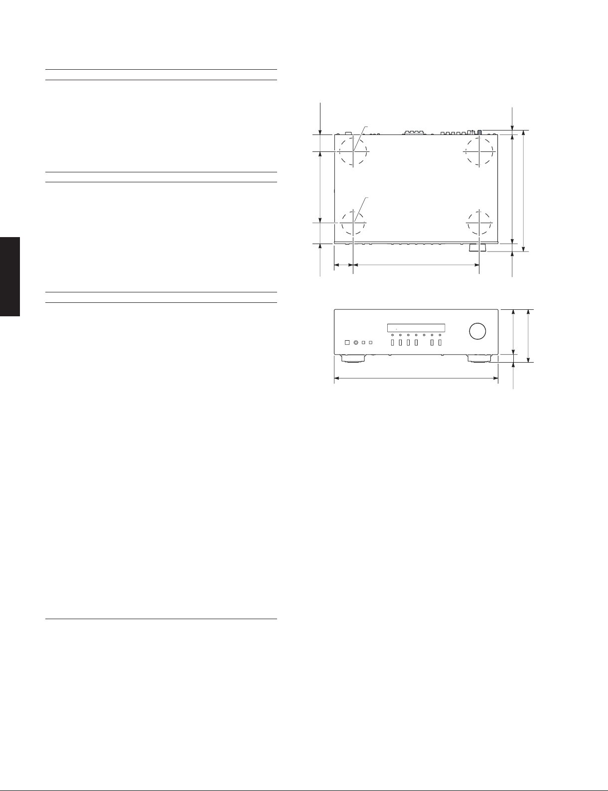
• DIMENSIONS
Top view
45
(1-3/4")
190 (7-1/2")
55
(2")
(2-1/8")
Front view
ø 71.6
ø 60
335 (13-1/4")50
435 (17-1/8")
11.5
(1/2")
322 (12-5/8")
290 (11-3/8")
20.5
(3/4")
120 (4-3/4")
21
(7/8")
Unit: mm (inch)
141 (5-1/2")
* Specifications are subject to change without notice.
U ........................U.S.A. model
C ................. Canadian model
R .................... General model
T.....................Chinese model
K ......................Korean model
A .................Australian model
B .......................British model
G ................. European model
L................. Singapore model
8
Page 9

■ INTERNAL VIEW
Top view
1 32
Front view
R-S202/R-S202D
a
SWITCH P.C.B. (R model)
b
MAIN (1) P.C.B.
c
TUNER Module (R-S202)
MAIN (8) P.C.B. + DAB Module (
d
MAIN (5) P.C.B.
e
MAIN (7) P.C.B.
f
POWER TRANSFORMER
g
MAIN (6) P.C.B.
h
MAIN (3) P.C.B.
i
MAIN (2) P.C.B.
j
BTCARD P.C.B.
k
MAIN (4) P.C.B.
456
A-S202D)
R-S202/R-S202D
8 9 j k7
■ SERVICE PRECAUTIONS
Safety measures
• Some internal parts in this product contain high voltages and are dangerous.
Be sure to take safety measures during servicing, such as wearing insulating gloves.
• Note that the capacitors indicated below are dangerous even after the power is turned off because an electric charge
remains and a high voltage continues to exist the
Before starting any repair work, connect a discharging resistor (5 k-ohms/10 W) to the terminals of each capacitor
indicated below to discharge electricity.
The time required for discharging is about 30 seconds per each.
C140, C143 and C149 on MAIN (1) P.C.B.
For details, refer to “PRINTED CIRCUIT BOARDS”.
.
re
9
Page 10

R-S202/R-S202D
■ DISASSEMBLY PROCEDURES
(Remove parts in the order as numbered.)
Disconnect the power cable from the AC outlet.
1. Removal of Top Cover
a. Remove screw (1), 4 screws (2) and 6 screws (3). (Fig. 1)
b. Remove the top cover. (Fig. 1)
2. Removal of Front Panel Unit
a. Remove 2 screws (4) and 6 screws (5). (Fig. 1)
b. Remove CB102, CB204, CB401 and CB502. (Fig. 1)
c. Release 2 hooks and then remove the front panel unit. (Fig. 1)
R-S202/R-S202D
2
Top cover
1
5
4
5
MAIN (6) P. C.B.
CB401
4
Hook
CB502
MAIN (2) P. C.B.
Front panel unit
3
2
CB102
CB204
MAIN (1) P. C.B.
5
Fi
g. 1
Hook
10
Page 11

3. Removal of AMP Unit
a. Remove 11 screws (7). (Fig. 3)
b. Remove 4 screws (8) and screw (9). (Fig. 2)
c. Remove CB4, CB7, CB103 and CB202. (Fig. 2)
d. Remove the AMP unit. (Fig. 2)
R-S202/R-S202D
8
9
CB4
CB7
CB103
8
8
R-S202/R-S202D
CB202
AMP unit
7
MAIN (1) P. C.B.
Fig. 2
Rear view
7
Fig. 3
11
Page 12

R-S202/R-S202D
When checking the MAIN (1) P.C.B.:
• Place the P.C.B.s (with rear panel) upright. (Fig. 4)
• Connect the heatsink and rear panel to the chassis with a ground lead or the like. (Fig. 4)
• Reconnect all cables (connectors) that have been disconnected.
• When connecting the flexible flat cable, be careful with polarity.
R-S202/R-S202D
MAIN (1) P.C.B.
Rear panel
Heatsink
Ground lead
Chassis
Ground lead
12
Fig. 4
Page 13

R-S202/R-S202D
■ UPDATING FIRMWARE
When the following parts are replaced, the firmware must be updated to the latest version.
MAIN P.C.B.
Microprocessor: IC203 on FUNCTION (1) P.C.B.
● Confirmation of firmware version and checksum
Before and after updating the firmware, check the firmware version and checksum by using the self-diagnostic
function menu.
Start up the self-diagnostic function and select “1. FIRMWARE VERSION/CHECK SUM” menu.
U
sing the sub-menu, have the firmware version and checksum displayed, and note them down.
(For details, refer to “SELF-DIAGNOSTIC FUNCTION”)
* When the firmware version is different from written one after updating, perform the updating procedure again from
the beginning.
● Initializing the back-up IC
After updating the firmware, the back-up IC MUST be initialized by the following procedure to store the setting
information properly.
Start up the self-diagnostic function and select “5. FACTORY PRESET” menu.
(For details, refer to “SELF-DIAGNOSTIC FUNCTION”)
Select “PRST RSRV”, press the “z” (Power) key to turn off the power once and turn on the power again. Then the
backup IC is initialized.
R-S202/R-S202D
● Required Tools
• Firmware downloader program
...................................................................RFP.exe
• Firmware
.....................................................RS_202_xxx.mot
• RS-232C conversion adaptor (Part No.:
ZK189200)
• Flexible flat cable
(9 pin 150 mm pitch = 1.25, Part No.: ZD896000)
• USB to Serial converter
(USB type-A to D-sub 9 pin)
* Recommendation: BUFFALO
(Part No.: BSU
F
(Part No.: DS-US232R-10)
TDI Ltd.
SRC0605BS)
● Preparation and precautions
• Download the firmware downloader program and
the latest firmware from the specified download
source to the same folder of the PC.
• Prepare the above specified RS-232C cross
cable.
• While writing the firmware, keep the other
application software on the PC closed.
It is also recommended to keep the software on
the task tray cl
osed as well.
13
Page 14

R-S202/R-S202D
● Connection
* Disconnect the power cable of this unit from the AC outlet.
• Connect the writing port (CB201 on MAIN (1) P.C.B.) located on the rear panel of this unit to the USB port of the PC
with USB to serial converter, RS-232C conversion adaptor and flexible flat cable as shown below. (Fig. 1)
This unit
USB to serial converter
R-S202/R-S202D
● Operation Procedures
1. Connect the power cable of this unit to the AC outlet.
The power to this unit is supplied and the microprocessor is in the writing mode.
2. Start up RFP.exe.
The screen appears as shown below. (Fig. 2)
3. Select the Basic mode and click [Next]. (Fig. 2)
PC
(CB201 on MAIN (1) P.C.B.)
Writing port
USB port
Flexible flat cable (9P)
RS-232C conversion adaptor
Fig. 1
Select Basic mode
14
Fig. 2
Page 15

4. Select the type of the microprocessor and make the workspace. (Fig. 3)
• Microcontroller: RL78
• Using Target Microcontroller: RL78/G13, R5F100JF
• Workspace Name: Any name
• Project Name: Any name
• Folder: Any place
* Click [Browse…] and specify the place where the workspace is made. (Fig.3)
5. Click [Next]. (Fig. 3)
R-S202/R-S202D
Fig. 5
Fig. 3
RL78
RL78/G13, R5F100JF
Workspace Name
Project Name
Folder
R-S202/R-S202D
15
Page 16

R-S202/R-S202D
6. Select COMx with the Tool and click [Next]. (Fig. 4)
* Do not proceed to other settings until clicking [Next] is completed. (Fig. 4)
Fig. 4
Tool: COMx
R-S202/R-S202D
7. Make the port (COMx) setting. (Fig. 5)
a. Access the device manager. (Fig. 5)
b. Right click the communication port (COMx) of the port (COM and LPT) to open the property. (Fig. 5)
c
. Using the port setting function, set the Bit/second to “115200”. (Fig. 5)
8. Click [OK]. (Fig. 5)
* To access the device manager, click [Start], [Control panel], [System], [Hardware] and [Device manager] in this
order.
* COMx: Enter the port number of the PC to which the USB to serial converter is connected in
place of “x”.
115200
16
Fig. 5
Page 17

9. Click [Browse...] and select the firmware name. (Fig. 6)
10. Click [Start] to start writing. (Fig. 6)
R-S202/R-S202D
R-S202/R-S202D
Writing being executed.
Fig. 6
17
Page 18

R-S202/R-S202D
11. When writing of the firmware is completed, the screen appears as shown below. (Fig. 7)
12. Click [X] to end RFP.exe. (Fig. 7)
R-S202/R-S202D
Fig. 7
13. Disconnect the power cable of this unit from the AC outlet.
14. Remove the RS-232C conversion adaptor and flexible flat cable from the writing port (CB201 on MAIN (1) P.C.B.) of
this unit.
15. Connect the power cable of this unit to the AC outlet, start up the self-diagnostic function and check that the firmware
version and checksum are the same as written ones. (For details, refer to “Con
checksum”)
firm
ation of firmware version and
18
Page 19

R-S202/R-S202D
■ SELF-DIAGNOSTIC FUNCTION
This unit has self-diagnostic functions that are intended for inspection, measurement and location of faulty point.
Each item has a main menu, each of which has sub-menu items.
Listed in the table below are main menu items and sub-menu items.
Note:
Some of the menu items listed below may not apply to the models covered in this service manual.
No. Main menu No. Sub-menu
1 VERSION/CHECK SUM 1 FIRMWARE VERSION
2 FIRMWARE CHECKSUM
3 MODEL/DESTINATION
4 BT VERSION
5 DAB VERSION (R-S202D)
2 DISPLAY CHECK 1 INITIAL DISPLAY
2 ALL SEGMENT OFF
3 ALL SEGMENT ON
3 Bluetooth 1 Bluetooth ADDRESS
2 Bluetooth LOOPBACK
3 Bluetooth NAME
4 DAB
(Not for service)
5 FACTORY PRESET 1 PRESET INHIBIT
6 AD DATA CHECK 1 PS
7 PROTECTION HISTORY 1 HISTORY 1
1 SIGNAL QUALITY
2 PRESET RESERVE
2 DC
3 TEMPERATURE A
4 TEMPERATURE B
DESTINAT
5
6 KEY 0 / KEY 1
ION
R-S202/R-S202D
(Not for service)
2 HISTORY 2
3 HISTORY 3
4 HISTORY 4
8 POWER OFF FACTOR HISTORY 1 LAST
2 HISTORY 1
3 HISTORY 2
4 HISTORY 3
5 HISTORY 4
19
Page 20

R-S202/R-S202D
● Starting Self-Diagnostic Function
While pressing the “BASS +” and “SPEAKERS A” keys, press the “z” (Power) key to turn on the power, and release those
2 keys.
The self-diagnostic function mode is activated.
“ ” (Power) key
R-S202/R-S202D
Keys of this unit
“ ” (Power) indicator
While pressing these keys, turn on the power.
● Starting Self-Diagnostic Function in the protection cancel mode
If the protection function works and causes hindrance to troubleshooting, cancel the protection function by the procedure
below, and it will be possible to enter the self-diagnostic function mode. (The protection functions other than the excess
current detect function will be disabled.)
While pressing the “BASS +” and “SPEAKERS A” key
those 2 keys and “z” (Power) key for 3 seconds or longer.
The self-diagnostic function mode is activated with the protection functions disabled.
In this mode, the “SLEEP” segment of the FL display flashes to indicate that the mode is self-diagnostic function mode with
the protection functions disabled.
CAUTION!
Using this unit with the protection function disabled may cause further damage to this unit. Use special care for this point
when using this mode.
ss the “z” (Power) key to turn on the power and keep pressing
s, pre
● Canceling Self-Diagnostic Function
1. Before canceling self-diagnostic function, execute setting for “5. FACTORY PRESET” menu. (Memory initialization
inhibited or Memory initialized).
* In order to keep the user memory preserved, be sure to select PRESET INHIBIT (Memory
2. Press the “z” (Power) key to turn off the power.
initialization inhibited).
20
Page 21

● Display provided when Self-Diagnostic Function started
Main menu displayOpening message
The display is as described below depending on the situation when the power to this unit is turned off.
1. When the power is turned off by usual operation:
“NO PROTECT” is displayed. Then “1. VERSION/SUM” is displayed in a few seconds.
NO PRT VER A01 U
After a few seconds
R-S202/R-S202D
2. When the protection function worked to turn off the power:
The information of protection function which worked at that time is displayed. Then “1. VERSION/SUM” is displayed in
a few seconds.
Note:
At that time if you restart the self-diagnostic function after turning off the power once, “NO PROTECT” will be
displayed. That is because that situation is equal to “1. When the power is turned off by usu
owever history of the protection function is stored in memory as backup data. For details, refer to “7.
H
PROTECTION HISTORY” menu.
2-1. When there is a history of protection function due to excess current.
al operation:”.
I PRT
Display:
Cause:
Supplementary information:
checking the current detect transistor.
Turning on the power without correcting the abnormality will cause the protection function to work immediately and the
power supply will instantly be shut off.
Notes:
• Applying the power to this unit without correcting the abnormality can be dangerous and cause additional
•
• Amplifier current should be monitored by measuring DC voltage across the emitter resistors for each channel.
The Power indicator is flashing.
An excessive current flowed through the power amplifier.
As current of the power amplifier is detected, the abnormal channel can be identified by
circuit damage. To avoid this, if protection function due to excess current works 1 time, the power will not turn
on even when the “z” (Power) key is pressed. In order to turn on the power again, disconnect the power cable
of this unit from the AC outlet once and then reconnect it again
The output transistors in each amplifier channel should be checked for damage before applying power to this
unit.
.
R-S202/R-S202D
21
Page 22

R-S202/R-S202D
2-2. When the protection function worked due to abnormal DC output.
Cause:
Supplementary information:
A cause could be a defect in the amplifier.
Turning on the power without correcting the abnormality will cause the protection function to work in 3 seconds and the
power supply will be shut off.
2-3. When the protection function worked due to abnormal voltage in the po
R-S202/R-S202D
Cause:
Supplementary information:
Turning on the power without correcting the abnormality will cause the protection function to work in 1 seconds and the
power supply will be shut off.
DC xxxL
DC output of the power amplifier is abnormal.
The protection function worked due to a DC voltage appearing at the speaker terminal.
PS xxxH
The voltage in the power supply section is abnormal.
The protection function worked due to a defect or overload in the power supply.
H: Displayed when the voltage is HIGHER than upper limit
L: Displayed when the voltage is LOWER than lower limit
xxx: A/D conversion value of voltage at the moment when the
protection function worked
(Reference voltage: 3.3 V = 255)
we
r supply section.
H: Displayed when the voltage is HIGHER than upper limit
L: Displayed when the voltage is LOWER than lower limit
xxx: A/D conversion value of voltage at the moment when the
protection function worked
Reference voltage: 3.3 V = 255)
(
Notes:
• Applying the power to this unit without correcting the abnormality can be dangerous and cause additional
circuit damage. To avoid this, if “PS” and “DC” protection function works 3 times consecutively, the power will
not turn on even when the “z” (Power) key is pressed. In order to turn on the power again, disconnect the
power cable of this unit from the AC outlet once and then reconnect i
t ag
ain.
• The output transistors in each amplifier channel should be checked for damage before applying power to this
unit.
• Amplifier current should be monitored by measuring DC voltage across the emitter resistors for each channel.
2-4. When the protection function worked due to excessive heatsink/bridge diode temperature.
H: Displayed when the voltage is HIGHER than upper limit
L: Displayed when the voltage is LOWER than lower limit
xxx: A/D conversion value of voltage at the moment when the
protection function worked
(Reference voltage: 3.3 V = 255)
TA: Heatsink
TB: Bridge diode (D113 on MAIN P.C.B.)
Cause:
The temperature of the heatsink/bridge diode (D113) is excessive.
Supplementary information:
TA xxxH
The protection function worked due to the temperature limit being exceeded. Causes could
be poor ventilation or a defect related to the thermal sensor.
Turning on the power without correcting the abnormality will cause the protection function to work in 1 second and the
power supply will be shut off.
22
Page 23

R-S202/R-S202D
Sub-menu selection
● History of protection function
When the protection function has worked, its history is stored in memory as backup data.
Even if no abnormality is noted while servicing the unit, an abnormality which has occurred previously can be defined
as long as the backup data has been stored.
For details, refer to “7. PROTECTION HISTORY” menu.
● Operation procedure of Main menu and Sub-menu
Each item has a main menu, each of which has sub-menu items.
Main menu selection
Select the main menu using “INPUT a” (forward) and “INPUT
Sub-menu selection
Select the sub-menu using “TREBLE +” (forward) and “TREBLE –” (reverse) keys.
Keys of this unit
Reverse
a
” (reverse) keys.
Main menu selection
● Functions in Self-Diagnostic Function mode
In addition to the self-diagnostic function menu items, functions listed below are available.
• Power ON/OFF
• Master volume
• SPEAKERS A ON/OFF
* Functions related to the tuner and the set menu are not available.
R-S202/R-S202D
drawroFesreveRdrawroF
The following initial settings are used when self-diagnostic function is started.
When self-diagnostic function is canceled, these settings are
• Master volume: 60
• Input: CD
• SPEAKER: SPEAKERS A on
● Initial settings when Self-Diagnostic Function started
restored to those before starting self-diagnostic function.
23
Page 24

R-S202/R-S202D
● Details of Self-Diagnostic Function menu
1. VERSION/CHECK SUM
This menu is used to display the firmware version and checksum.
The checksum is obtained by adding the data at every 8-bit and expressing the result as a 4-digit hexadecimal
notation.
* Numeric values in the figure are given as reference only.
1-1. FIRMWARE VERSION
VER A10 U
The firmware version of the microprocessor (IC203 on MAIN (1) P.C.B.) and
destination are displayed.
Not for service.
R-S202/R-S202D
SUM 060C
R -U(013)
B 3.05
D N/A
1-2. FIRMWARE CHECKSUM
The checksum value of the microprocessor (IC203 on MAIN (1) P.C.B.) is displayed.
1-3. MODEL/DESTINATION
The model name and destination are displayed.
Not for service.
Destination: U (U, C), R, T, A, B, G, L
Model
Model name
1-4. BLUETOOTH VERSION
The firmware version of the Bluetooth module is displayed.
1-5. DAB VERSION (R-S202D)
The firmware version of the DAB module is displayed.
R (R-S202)
RD (R-S202D)
24
Page 25

2. DISPLAY CHECK
2-1. INITIAL DISPLAY
This menu is used to check operation of the FL display.
Using the sub-menu, the display varies as shown below.
2-2. ALL SEGMENT OFF
R-S202/R-S202D
FL display
R-S202/R-S202D
Segment conditions of the FL driver and the FL tube are checked by turning ON and OFF all segments.
2-3. ALL SEGMENT ON
After check, change to next sub-menu at once.
*
If you turn ON all segments for a long period,
it may cause trouble.
25
Page 26

R-S202/R-S202D
3. Bluetooth
The infomation of the Bluetooth module is displayed.
3-1. Bluetooth ADDRESS
3-2. Bluetooth LOOPBACK
3-3. Bluetooth NAME
R-S202/R-S202D
4. DAB
Not for service.
4-1. SIGNAL QUALITY
The address of the Bluetooth module is displayed.
3481F4-
Not for service.
B UART NG
The writing of memory is checked in Bluetooth module.
B NAME OK
OK: Normal
NG: Writing abnormal
--: Checking
D SIQ N/A
5. FACTORY PRESET
This menu is used to reserve/inhibit initialization of the back-up IC.
PRST INHI
PRST RSRV
CAUTION:
3-1. PRESET INHIBIT
Initialization of the back-up IC is not executed. Select this sub-menu to protect the
values set by the user.
3-2. PRESET RESERVED
Initialization of the back-up IC is reserved. (Actual initialization is executed when the
power is turned on next.)
To reset to the original factory settings or to reset the backup IC, select this sub-menu
and press the “z” (Power) key to turn off t
Before setting to the PRESET RESERVED, write down the existing preset memory content of the tuner. (This is
because setting to the PRESET RESERVED will cause the user memory content to be erased.)
(Initialization inhibited)
(Initialization reserved)
he power.
26
Page 27

R-S202/R-S202D
6. AD DATA CHECK
This menu is used to display the A/D conversion value of the microprocessor which detects panel keys and protection
functions by using the sub-menu.
When “6-6. KEY” sub-menu is selected, keys become inoperable due to detection of the values of all keys. However,
it is possible to advance to the next menu by pressing the “ ▲ ” (forward) key or “ ▼ ” (reverse) key on the remote
control.
*
Numeric values in the figure
6-1. PS
Power supply voltage (PS) protection detection.
The voltage at 44 pin (PRPS) of IC203 is displayed.
Normal value: 113 to 174
(Reference voltage: 3.3 V = 255)
* If PS becomes out of the normal value range, the protection function works to turn off the power.
are given as reference only.
PS 148
6-2. DC
Power amplifier DC (DC voltage) output is detected.
The voltage at 42 pin (PRD) of IC203 is displayed.
Normal value: 27 to 136
(Reference voltage: 3.3 V = 255)
* If DC becomes out of the normal value range, the protection function works to turn off the power.
R-S202/R-S202D
DC 088
6-3. TEMPERATURE A
Temperature of the heatsink is detected.
The voltage at 43 pin (THM1) of IC203 is displayed.
Normal value: 15 to 134
(Reference voltage: 3.3 V = 255)
* If TA becomes out of the normal value range, the protection function works to turn off the power.
TA 071
6-4. TEMPERATURE B
Temperature of the bridge diode is detected.
The voltage at 2 pin (THM2) of IC203 is displayed.
Normal value: 15 to 130
(Reference voltage: 3.3 V = 255)
* If TB becomes out of the normal value range, the protection function works to turn off the power.
TB 237
27
Page 28

R-S202/R-S202D
6-5. DESTINATION
The destination is displayed.
6-6. KEY0 / KEY1
Panel key is detected.
KEY0: The voltage at 40 pin (KEY0) of IC203 is displayed.
KEY1: The voltage at 41 pin (KEY1) of IC203 is displayed.
When the A/D conversion value of the panel key becomes out of the specified range, normal operation will not
be available.
In that case, check the constant of voltage dividing resistor, solder condition, etc. Refer to table.
* When “6-6. KEY” menu i
H
on the remote control.
(Reference voltage: 3.3 V = 255)
DEST xxx
s selected, keys become inoperable due to detection of the values of all keys.
owever, it is possible to advance to the next menu by pressing the “ ▲ ” (forward) key or “ ▼ ” (reverse) key
R-S202/R-S202D
K-255,255
KEY1
KEY0
Display KEY0 Display KEY1
000 – 011 INPUT a 000 – 011 TUNING
012 – 032 INPUT
033 – 054 TREBLE + 033 – 054 PRESET
055 – 079 TREBLE – 055 – 079 PRESET
080 – 107 BASS + 080 – 107 BAND
108 – 134 BASS – 108 – 134 MEMORY
135 – 160
a
012 – 032 TUNING
135 – 160 FM MODE
161 – 187 SPEAKER A
28
188 – 214 SPEAKER B
Page 29

7. PROTECTION HISTORY
This menu is used to display the history of protection function.
When the “SPEAKERS B” key is pressed, the protection history being displayed will be cleared.
* Numeric values in the figure are given as reference only.
R-S202/R-S202D
1 PS xxxH
2 DC xxxL
3 TA xxxH
4 NO PRT
7-1. HISTORY 1
H: Displayed when the voltage is HIGHER than upper limit
L: Displayed when the voltage is LOWER than lower limit
xxx: A/D conversion value of voltage at the moment when the protection function worked
(Reference voltage: 3.3 V = 255)
7-2. HISTORY 2
7-3. HISTORY 3
7-4. HISTORY 4
8. POWER OFF FACTOR HISTORY
This menu is used to display the history of power off factor.
R-S202/R-S202D
6-1 PANEL
6-2 REM
6-3 SLEEP
6-4 APS
6-5 ---
8-1. LAST
8-2. HISTORY 1
8-3. HISTORY 2
8-4. HISTORY 3
8-5. HISTORY 4
Power off factor are as follows.
6-x PANEL “z” (Power) key of this unit
6-x REM “z” (Power) key on the remote control
6-x SLEEP SLEEP timer
6-x APS Auto Power Standby
6-x PRT Protection
6-x AC AC OFF
6-x BT Bluetooth no operation
6-x --- No history
29
Page 30

R-S202/R-S202D
1
32
1G
■ DISPLAY DATA
● V501 : 010ST027GNK (MAIN P.C.B.)
● PIN CONNECTION
Pin No.
Connection
32 31 30 29 28 27 26 25 24 23 22 21
F2 F2 NP 1G 2G 3G 4G 5G 6G 7G 8G 9G
PATTERN AREA
R-S202/R-S202D
● GRID ASSIGNMENT
● ANODE CONNECTION
Pin No.
Connection
Note
20 19 18 17 16 15 14 13 12 11 10 9 8 7 6 5 4 3 2 1
10G P16 P15 P14 P13 P12 P11 P10 P9 P8 P7 P6 P5 P4 P3 P2 P1 NP F1 F1
: 1) Fn ..... Filament pin 2) nG ..... Grid pin 3) Pn ..... Anode pin 4) NP ..... No pin
2G 3G 4G 5G 6G
7G 8G 9G 10G
1G 2G – 10G
P1 MHz s2
P2 kHz s1
P3 ST a
P4 SLEEP b
P5 TUNED f
P6 SP A h
P7 SP B j
P8 MEMORY k
P9 PRESET g
P10 m
P11 c
P12 e
P13 r
P14 p
P15 n
P16 d
g
f
e
s1
a
j
p
d
(2G–10G)
s2
kh
b
m
c
n r
30
Page 31
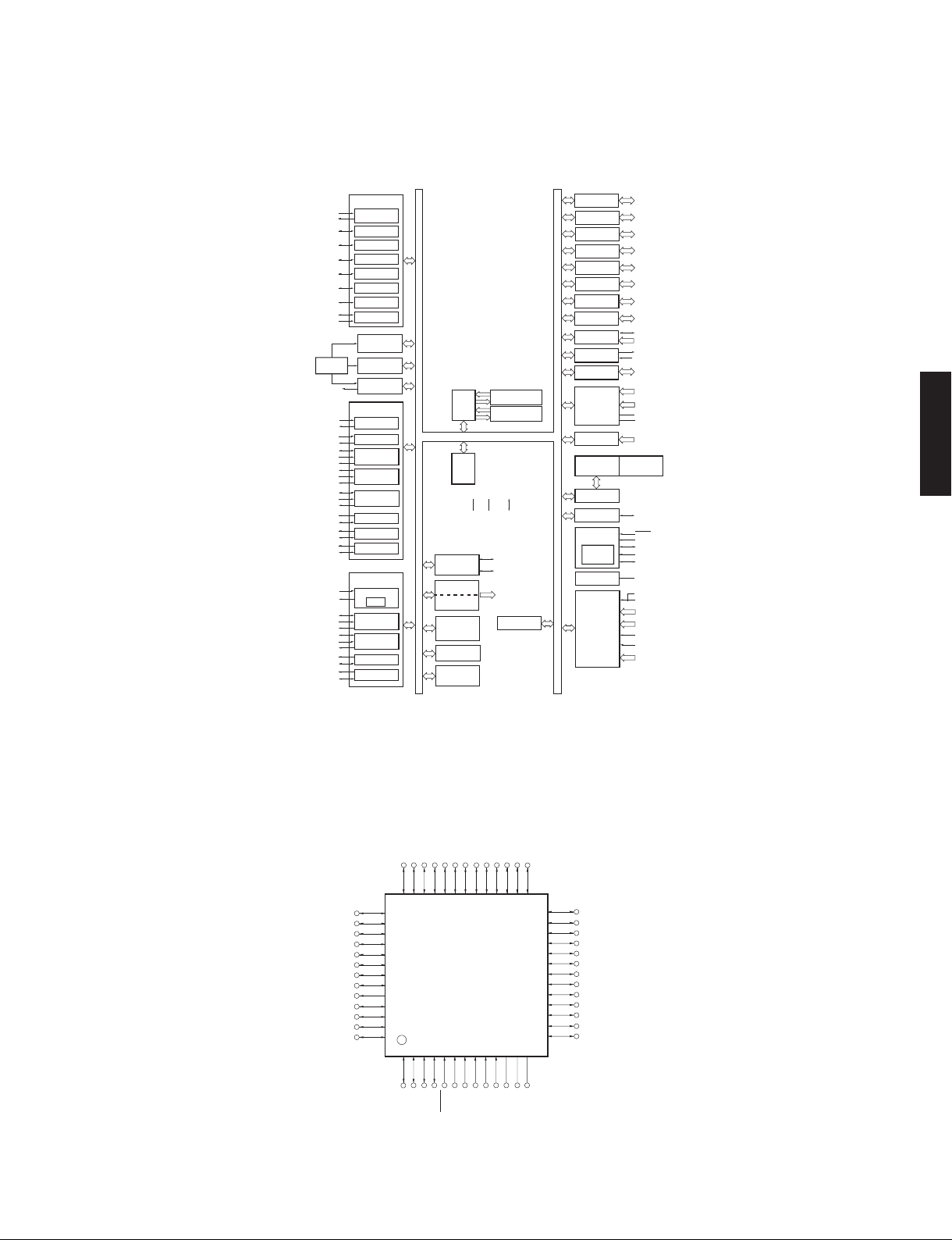
■ IC DATA
IC203:
R5F100JFAFA (MAIN (1) P.C.B.)
Microprocessor
* No replacement part available.
R-S202/R-S202D
TI00/P00
TO00/P01
TI01/TO01/P16
TI02/TO02/P17
(TI02/TO02/P15)
TI03/TO03/P31
(TI03/TO03/P14)
(TI04/TO04/P13)
(TI05/TO05/P12)
(TI06/TO06/P11)
TI07/TO07/P41
(TI07/TO07/P10)
RxD2/P14
(RxD2/P76)
LOW-SPEED
ON-CHIP
OSCILLATOR
RTC1HZ/P30
RxD0/P11(RxD0/P16)
TxD0/P12(TxD0/P17)
RxD1/P03
TxD1/P02
SCK00/P10
SI00/P11
SO00/P12
SCK01/P75
SI01/P74
SO01/P73
SCK11/P30
SI11/P50
SO11/P51
SCL00/P10
SDA00/P11
SCL01/P75
SDA01/P74
SCL11/P30
SDA11/P50
RxD2/P14(RxD2/P76)
TxD2/P13(TxD2/P77)
SCK20/P15
SI20/P14
SO20/P13
SCK21/P70
SI21/P71
SO21/P72
SCL20/P15
SDA20/P14
SCL21/P70
SDA21/P71
TIMER ARRAY
UNIT (8ch)
ch0
ch1
ch2
ch3
ch4
ch5
ch6
ch7
WINDOW
WATCHDOG
TIMER
12-BIT INTERVAL
TIMER
REAL-TIME
CLOCK
SERIAL ARRAY
UNIT0 (4ch)
UART0
UART1
CSI00
CSI01
CSI11
IIC00
IIC01
IIC11
SERIAL ARRAY
UNIT1 (2ch)
UART2
LINSEL
CSI20
CSI21
IIC20
IIC21
RL78
CPU
CORE
RAM
SERIAL
INTERFACE IICA0
BUZZER OUTPUT
CLOCK OUTPUT
CONTROL
MULTIPLIER&
DIVIDER,
MULITIPLY-
ACCUMULATOR
DIRECT MEMORY
ACCESS
CONTROL
BCD
ADJUSTMENT
VSSTOOLRxD/P11,
V
DD
2
CODE FLASH MEMORY
DATA FLASH MEMORY
TOOLTxD/P12
SDAA0/P61(SDAA0/P13)
SCLA0/P60(SCLA0/P14)
PCLBUZ0/P140
(PCLBUZ0/P31),
PCLBUZ1/P15
CRC
PORT 0
PORT 1
PORT 2
PORT 3
PORT 4
PORT 5
PORT 6
PORT 7
PORT 12
PORT 13
PORT 14
A/D CONVERTER
KEY RETURN
POWER ON RESET/
VOLTAGE
DETECTOR
RESET CONTROL
ON-CHIP DEBUG
SYSTEM
CONTROL
HIGH-SPEED
ON-CHIP
OSCILLATOR
VOLTAGE
REGULATOR
INTERRUPT
CONTROL
4
P00 to P03
8
P10 to P17
8
P20 to P27
2
P30, P31
2
P40, P41
2
P50, P51
4
P60 to P63
8
P70 to P77
P120
4
P121 to P124
P130
P137
P140,
3
P146, P147
ANI0/P20 to
8
ANI7/P27
ANI16/P03, ANI17/P02,
4
ANI18/P147, ANI19/P120
AV
/P20
REFP
AV
REFM
/P21
KR0/P70 to
8
KR7/P77
POR/LVD
CONTROL
TOOL0/P40
RESET
X1/P121
X2/EXCLK/P122
XT1/P123
XT2/EXCLKS/P124
REGC
RxD2/P14 (RxD2/P76)
INTP0/P137
INTP1/P50,
2
INTP2/P51
INTP3/P30,
2
INTP4/P31
INTP5/P16
INTP6/P140
INTP8/P74 to
4
INTP11/P77
R-S202/R-S202D
P27/ANI7
P26/ANI6
P25/ANI5
P24/ANI4
P23/ANI3
P22/ANI2
P21/ANI1/AV
P20/ANI0/AV
P130
P03/ANI16/RxD1
P02/ANI17/TxD1
P01/TO00
P00/TI00
P147/ANI18
P146
P10/SCK00/SCL00/(TI07)/(TO07)
P11/SI00/RxD0/TOOLRxD/SDA00/(TI06)/(TO06)
P12/SO00/TxD0/TOOLTxD/(TI05)/(TO05)
P13/TxD2/SO20/(SDAA0)/(TI04)/(TO04)
P14/RxD2/SI20/SDA20/(SCLA0)/(TI03)/(TO03)
P15/PCLBUZ1/SCK20/SCL20/(TI02)/(TO02)
P16/TI01/TO01/INTP5/(RXD0)
P17/TI02/TO02/(TXD0)
P51/INTP2/SO11
P50/INTP1/SI11/SDA11
P30/INTP3/RTC1HZ/SCK11/SCL11
39 38 37 36 35 34 33 32 31 30 29 28 27
40
41
42
43
44
45
REFM
REFP
46
47
48
49
50
51
52
26
P70/KR0/SCK21/SCL21
25
P71/KR1/SI21/SDA21
24
P72/KR2/SO21
23
P73/KR3/SO01
22
P74/KR4/INTP8/SI01/SDA01
21
P75/KR5/INTP9/SCK01/SCL01
20
P76/KR6/INTP10/(RXD2)
19
P77/KR7/INTP11/(TXD2)
18
P31/TI03/TO03/INTP4/(PCLBUZ0)
17
P63
16
P62
P61/SDAA0
15
P60/SCLA0
14
1 2 3 4 5 6 7 8 9 10 11 12 13
SS
DD
V
V
P123/XT1
P137/INTP0
REGC
P121/X1
P122/X2/EXCLK
RESET
P40/TOOL0
P120/ANI19
P41/TI07/TO07
P140/PCLBUZ0/INTP6
P124/XT2/EXCLKS
31
Page 32

R-S202/R-S202D
Pin
No.
1 P140/PCLBUZ0/INTP6 HPRY O O HP relay (LOW = OFF)
2 P120/ANI19 THM2 I I Temperature protection detection
3 P41/TI07/TO07 BT_MFB O O Bluetooth Multi-Function Push Button Key
4 P40/TOOL0 TOOL0 I I For E1 debugging
5 RESET N_RST I I For debugging
6 P124/XT2/EXCLKS (Vacant)
7 P123/XT1 (Vacant)
8 P137/INTP0 REM I IRQ IR light receiving unit
9 P122/X2/EXCLK (Vacant)
10 P121/
11 REGC REGC I I Regulator (Connected to VSS via capacitor)
12 VSS VSS I I GND
13 VDD VDD I I +5V power supply
14 P60/SCLA0 TU_SCL I I2C Tuner pack
15 P61/SDAA0 TU_SDA I I2C Tuner pack
16 P62 TU_N_RST O O Tuner pack
R-S202/R-S202D
17 P63 (Vacant)
18 P31/TI03/TO03/INTP4/(PCLBUZ0) PRI I I I protection detection
19 P77/KR7/INTP11/(TXD2) TU_GPIO2 I IRQ Tuner pack
20 P76/KR6/INTP10/(RXD2) (Vacant)
21 P75/KR5/INTP9/SCK01/SCL0
22 P74/KR4/INTP8/SI01/SDA01 EVOL_SDA I I2C VOL IC
23 P73/KR3/SO01 FL_STB O O FL Driver
24 P72/KR2/SO21 FL_MOSI O SPI FL Driver
25 P71/KR1/SI21/SDA21 FL_MISO O SPI FL driver (spare)
26 P70/KR0/SCK21/SCL21 FL_SCK O SPI FL Driver
27 P30/INTP3/RTC1HZ/SCK11/SCL11 PRY O O Power relay control
28 P50/INTP1/SI11/SDA11 MPSW I IRQ Main power SW (Tact SW)
29 P51/INTP2/SO11 PWR_DET I IRQ Power detect (LOW = AC-OFF)
30 P17/TI02/TO02/(TXD0) V
31 P16/TI01/TO01/INTP5/(RXD0) VOL_RB I I Volume encoder counterclockwise
32 P15/PCLBUZ1/SCK20/SCL20/(TI02)/(TO02) (Vacant)
33 P14/RxD2/SI20/SDA20/(SCLA0)/(TI03)/(TO03) REC_N_MUTE O O REC OUT mute (LOW = MUTE ON)
34 P13/TxD2/SO20/(SDAA0)/(TI04)/(TO04) PRE_N_MUTE O O PRE OUT mute (LOW = MUTE ON)
35 P12/SO00/TxD0/TOOLTxD/(TI05)/(TO05) (Vacant)
36 P11/SI00/RxD0/TOOLRxD/SDA00/(TI06)/(TO06) (Vacant
3
7 P10/SCK00/SCL00/(TI07)/(TO07) PLED O O Power LED (LOW = OFF)
38 P146 3.3S_PON O O Power supply (VFD driver power supply)
39 P147/ANI18 MODEL I I Model discrimination (LOW=R-S202 / HIGH=R-S202D)
40 P27/ANI7 KEY0 I I INPUT (
41 P26/ANI6 KEY1 I I SPEAKERS (A, B) / FM MODE / MEMORY / BAND / PRESET (<, >)
42 P25/ANI5 PRD I I DC protection detection (AMP DC / Voltage detection)
24/ANI4 T
43 P
44 P23/ANI3 PRPS I I PS protection detection (Power supply / Power voltage detection)
45 P22/ANI2 TEST
46 P21/ANI1/AVREFM VREFM I I Analog reference voltage minus
47 P20/ANI0/AVREFP VREFP I I Analog reference voltage plus
48 P130 SPBRY O O Speaker B relay ON/OFF (LOW = OFF)
49 P03/ANI16/RxD1 BT_MISO I UART ISSC BT Module
50 P02/ANI17/TxD1 BT_MOSI O UART ISSC BT Module
01/TO00 B
51 P
52 P00/TI00 SPARY O O Speaker A relay ON/OFF (LOW = OFF)
Port Name
X1 B
1 EVOL_SCL I I2C VOL IC
Function
Name
T_AMP_EN I I Bluetooth Amp Enable (Mute ON/OFF)
OL_RA I I Vo
)
HM1 I I Temperature protection detection (Thermal detection)
T_N_RST O O Bluetooth Reset
I/O
Related Power Supply
OFF ON
lume encoder clockwise
a
, a) / BASS (+, -) / TREBLE (+, -)
/ TUNING (<<, >>)
Detail of Function
32
Page 33

Key detection for A/D port
Key input (A/D) pull-up resistance 10 k-ohms
0 Ω + 1.0 k Ω + 1.0 k Ω + 1.5 k Ω + 2.2 k Ω + 3.3 k Ω + 4.7 k Ω
Detected voltage
value at 40 pin
A/D value
(3.3 V=255)
KEY0
Detected voltage
value at 41 pin
A/D value
(3.3 V=255)
KEY1
0 – 0.22 V
000 – 011 012 – 032 033 – 054 055 – 079 080 – 107 108 – 134 135 – 160
INPUT
a
0 Ω + 1.0 k Ω + 1.0 k Ω + 1.5 k Ω + 2.2 k Ω + 3.3 k Ω + 4.7 k Ω
0 – 0.14 V 0.15 – 0.42 V 0.43 – 0.7 V 0.71 – 1.02 V 1.03 – 1.38 V 1.39 – 1.73 V 1.74 – 2.07 V
000 – 011 012 – 032 033 – 054 055 – 079 080 – 107 108 – 134 135 – 160
TUNING
0.23 – 0.64 V 0.65 – 1.06 V 1.07 – 1.55 V 1.56 – 2.09 V 2.10 – 2.62 V 2.63 – 3.12 V
INPUT
a
TUNING PRESET PRESET
TREBLE
+
TREBLE
–
R-S202/R-S202D
BASS
+
BAND MEMORY FM MODE
BASS
–
R-S202/R-S202D
Detected voltage
value at 41 pin
A/D value
(3.3 V=255)
KEY1
+ 7.5 k Ω + 15 k Ω
2.08 – 2.41 V 2.42 – 2.77 V
161 – 187 188 – 214
SPEAKER
A
SPEAKER
B
33
Page 34

R-S202/R-S202D
R-S202/R-S202D
MEMO
34
Page 35

JIHGFEDCBA
R-S202/R-S202D
1
2
■ BLOCK DIAGRAMS
BluetoothModule
(BM20)
INT CLK:72MHz
BT_N_RST
BT_AMP_EN
BT_MFB
Audio Section Block Diagram
FM/AM
INT CLK:428.7MHz
CD A
3
LINE 1 B
X
POWER
AMPLIFIER
VOLUME
LINE 2
INPUT SELECTOR
TONE CONTROL
PRE_N_MUTE
SPARY
SPBRY
HPRY
RY102
RY103
RY101
SPEAKERS
PHONES
LINE 3
IC202
4
REC
X
Vol IC
BD3491FS
27
28
EVOL_SCL
EVOL_SDA
REC_N_MUTE
PRD
PRI
<interrupt> <serial>
REM INTP0UART1 BT Module
MPSW INTP1 I2CA0 Tuner
PWR_DETINTP2 I2C01 VOL IC
5
FL Driver
FL Display
HT16515
Remote Control
6
Volume
FL_MOSI TU_GPIO2 INTP11 SPI FL Driver
FL_MISO
<AD>
KEY0 ANI7
KEY1 ANI6
PRDANI5
REM THM1 ANI4 PWR_DET
THM2 ANI19 N_RST
PRPS ANI3
DEST ANI2
40
41
42
43
2
44
45
Microprocessor
IC203
R5F100JFAFA
Internal CLK:32MHz
MVOL_RA
MVOL_RB N_RST RESET
51
Main Power
Supply
(Main Transformer)
Standby
Power Supply
(Sub Transformer)
PRY
AC IN
KEY0
Push Key
KEY1 MPSW N_RST
Force Reset
MPSW
7
35
Page 36

R-S202/R-S202D
JIHGFEDCBA
1
2
3
4
5
6
7
IC1IC203
+3.3M
Sub Transformer
RY1
PRY
Power Supply Section Block Diagram
Microprocessor
Q209
3.3S_PON
+3.3MMicroprocessor (IC203), Remote,
Key Input, Rotary Encoder
+3.3STHM, FL Driver,
Control circuit around Microprocessor
+B Power Amplifier
S1
120V / 230V /
220・240V /
110-120・220-240V /
50・60 Hz
RY1
F1
D7
-B Power Amplifier
15V Q124 +8.44V Volume IC
Q123
-24VPFL Driver
+8.44V Bluetooth OP AMP
Q121 +3.3TTuner
+3.3BT Bluetooth
S2
F1 FL Filament
F2 FL Filament
36
Page 37

JIHGFEDCBA
R-S202/R-S202D
1
■ WIRING DIAGRAM
CB501
• OVERALL ASSEMBLY
CB902
MAIN (1)
(R-S202D)
to MAIN (8)
2
MAIN (5)
Top view
R model
Tie AC cable and all wire from
power transformer together.
CB3
SWITCH
R model
Top view
Tie AC cable and all wire from
power transformer together.
CB204
3
R-S202: TUNER Module
R-S202D: MAIN (8) P.C.B. + DAB Module
CB4
CB7
CB4
CB7
MAIN (1)
to MAIN (1) (CB102)
CB204
(CB602)
CB202
CB102
Side view
W102
4
POWER
TRANSFORMER
POWER
TRANSFORMER
CB103
MAIN (7)
W250
CB101
Avoid all wire from
touching heatsink.
MAIN (5)
Stick FFC 18p
with MAIN (8) P. C.B.
CB401
60 mm
5
CB502
MAIN (6)
Avoid wire from touching
power transformer.
60 mm
Front panel (View A)
6
MAIN (3)MAIN (6)
W501
MAIN (2)
to MAIN (2) (CB501)
to BTCARD (CB902)
MAIN (4)
View A
W502B
MAIN (2)
W502A
CB02
W503A
CB501
to MAIN (1)
(CB204)
W503B
CB902
7
BTCARD
37
Page 38

R-S202/R-S202D
JIHGFEDCBA
1
2
3
4
5
6
7
■ PRINTED CIRCUIT BOARDS
MAIN (1)
(Side A)
POWER TRANSFORMER POWER cable
CB4
CB5CB6
T, A, G, L models
CB7
Safety measures
• Some internal parts in this product contain high voltages and are dangerous. Be sure to take safety measures during
servicing, such as wearing insulating gloves.
• Note that the capacitors indicated below are dangerous even after the power is turned off because an electric charge
remains and a high voltage continues to exist there. Before starting any repair work, connect a discharging resistor
(5 k-ohms/10 W) to the terminals of each capacitor indicated below to discharge electricity. The time required for
discharging is about 30 seconds per each.
C140, C143 and C149 on MAIN (1) P.C.B.
SPEAKERS
A/B
R
+- -+
L
3
OUT IN
LINE
21
安全対策
・ この製品の内部には高電圧部分があり危険です。修理の際は、絶縁性の手袋を使用するなどの安全対策を行ってください。
・ 下記のコンデンサには電源を OFF にした後も電荷が残り、高電圧が維持されており危険です。修理作業前に放電用抵抗
(5 k Ω /10 W)を下記の各コンデンサの端子間に接続して放電してください。放電所用時間は各々約 30 秒間です。
MAIN(1)P.C.B. の C140、C143、C149
BT CARD
(CB902)
CD
BTAUDIO_R
L/RL/RL/RL/RL/R
BTAUDIO_L
GND
AOHPM
GND
CB102
BT_3.3V
BT_MISO
BT_MFBNCBT_N_RST
UART_TX_IND
BT_AMP_EN
GND
BT_MOSI
GND
Writing port
CB201
CB202
Power
transformer
Lch
Rch
GND
NC
+3.3V
N_INT
SCL
N_RST
R-S202:
SDA
AM/FM TUNER
R-S202D:
MAIN (8)
(CB602)
VPE
R model
U, C, T, A, G, L models
HPR
E
E
HPL
W102
CB101
CB204
3.3M
MG
FL_STB
FL_SCK
M_PLED
KEY0
MVOL_RA
-24V
MG
3.3S
FL_MISO
FL_MOSI
REM
MPSW
KEY1
MVOL_RB
MAIN (2)
(CB501)
MAIN (6)
(CB401)
R model
5 k-ohms
10 W
POWER TRANSFORMER
CB103
5 k-ohms
10 W
5 k-ohms
10 W
MG
3.3S
THM
MAIN (7)
(W250)
• Semiconductor Location
Ref no. Location
D113 E6
D7 C4
Q105 C5
Q106 F5
Q109 C5
Q110 C5
Q111 F5
Q112 F5
38
Page 39

JIHGFEDCBA
R-S202/R-S202D
1
Ref no. Location
D110 C3
D111 F5
D112 F5
D114 E3
MAIN (1)
(Side B)
D115 F5
D117 D3
D119 F5
D120 F4
D125 D4
2
D126 D4
D127 D5
D128 G5
T, A, G, L models
R model
D2 B5
D202 G5
D203 H5
D204 H5
D207 H4
D3 B5
D4 B4
D5 B4
3
D6 B5
D8 B4
D9 B4
116
IC202
32 17
14
IC102
85
IC1 B5
IC102 G4
IC202 G3
IC203 H4
Q1 B5
Q101 D5
Q102 F5
4
13 14
1
52
IC203
26
27
3940
Q103 D5
Q104 F5
Q107 C5
Q108 F5
Q117 C6
Q118 F6
Q119 G6
Q120 F4
Q121 G5
Q122 I4
1
5
R model
IC1
534
Q123 D5
Q124 F5
Q125 C4
Q126 F4
Q128 C4
Q129 F4
Q131 F5
Q133 C4
Q2 B4
Q201 F3
• Semiconductor Location
6
Ref no. Location
D1 B5
D10 B4
D101 G4
D102 I4
D103 D5
D104 G5
D105 C6
D106 F6
D107 G4
7
D108 F5
D109 D4
Q202 F3
Q203 F4
Q204 G4
Q205 I3
Q206 I3
Q208 H5
Q209 H5
Q3 B4
Q4 B5
Q5 B5
Q6 B5
Q7 B5
Q8 C5
39
Page 40

R-S202/R-S202D
JIHGFEDCBA
1
2
3
4
5
6
7
MAIN (2)
POWER TRANSFORMER
MG
SW_SPAB
MP_SW
3.3M
CB502
Remote control
sensor
W502A
(Side A)
STANDBY/ON
indicator
CB501
MVOL_RA
KEY0
M_PLED
FL_SCK
FL_STB
MG
3.3M
VPE
MVOL_RB
KEY1
MPSW
REM
FL_MOSI
FL_MISO
3.3S
MG
-24V
MAIN (1)
(CB204)
chassis
FM MODE
W501
MEMORY BAND PRESET TUNING
W503A
3.3M
VOL_RA
VOL_RB
MG
SW_PDRT
FG
MAIN (3)
(Side A)
3.3MMGSW_SPAB
MP_SW
W502B
VOL_RA
VOL_RB
SW_PDRT
(Power)
AB
SPEAKERS
+3.3M
MG
FG
INPUTTREBLEBASS +–+–
MAIN (4)
VOLUME
W503B
(Side A)
• Semiconductor Location
Ref no. Location
D511 D2
D514 G2
40
Page 41

JIHGFEDCBA
R-S202/R-S202D
1
MAIN (2)
2
(Side B)
22 23
12
11
IC501
33
34
441
3
4
MAIN (4)
5
MAIN (3)
(Side B)
(Side B)
6
• Semiconductor Location
Ref no. Location
D501 D2
D502 D2
IC501 F2
Q502 E2
7
Q503 D3
Q504 G2
41
Page 42
R-S202/R-S202D
JIHGFEDCBA
1
2
3
4
5
6
7
MAIN (5)
(Side A)
MAIN (6)
(Side A)
MAIN (7)
(Side A)
CB401
PHL
HPR
HPE
HPL
MAIN (1)
(W102)
W250
VCC
OUT
GND
IC250
MG
3.3S
THM
MAIN (1)
(CB101)
PHONES
MAIN (8)
(Side A)
(R-S202D)
CB602
NC
SDA
GND
+3.3V
NC
Lch
Rch
SCL
N_RST
MAIN (1) (CB202)
• Semiconductor Location
Ref no. Location
IC250 I2
42
Page 43

JIHGFEDCBA
R-S202/R-S202D
1
MAIN (5)
2
3
4
(Side B)
MAIN (6)
(Side B)
MAIN (7)
(Side B)
MAIN (8)
(R-S202D)
(Side B)
SWITCH
(Side A)
R model
5
6
7
VOLTAGE
SELECTOR
110–120V220–230V
CB3
YELLOW
PURPLE
POWER
TRANSFORMER
ORANGE
RED
43
Page 44

R-S202/R-S202D
• ICs
■ PIN CONNECTION DIAGRAMS
33
17
32
1
34
16
44
1
23
22
12
11
LM61CIZ NJM2904MBD3491FS-E2 HT16515-44LQFP R5F100JFAFA R1190H033B-T1-FE
39
40
8
+V
S
OUT
V
GND
4
1
52
1
27
26
14
13
1
3
5
4
• Diodes
Anode
Cathode
Anode
Cathode
Anode
+
–
–
AC
AC
+
AC
AC
Cathode
• Transistors
2N5401S-RTK/P 3LN01C-TB-E2SC5712
2N5551S-RTK/P
2SA1037K
2SA1037K Q,R,S
2SA1514K R,S
2SC3906K
2SC2412K
2SC2712-GR
2SD2704 K
C
B
DTC014EUBTL
E
C
E
B
KTA1661-Y-RTF/P
C
B
KTC3206Y-ATP
C
E
B
KTA1664-Y-RTF/P
KTC4376-Y-RTF/P
2SC4468
E
B
C
E
KTB631K Y, GR
KTD600K-Y-U/PH
MCH6336-TL-E
UDZV2.4BBAV103 F3A501BDV006A506ABS5D1SS352 TE
UDZV3.9B
UDZV4.7B
UDZV9.1B
UDZV12B
UDZV15B
UDZV24B
UDZV36B
B
C
E
Cathode
Anode
D
S
G
44
3
2
1
1: IN
2: GND
3: OUT
B
C
E
E
C
B
E
C
B
4
6
1
3
1. Drain
2. Drain
3. Gate
4. Source
5. Drain
6. Drain
Page 45

A
VB
KJIHGFEDCB
L
NM
R-S202/R-S202D
■ SCHEMATIC DIAGRAMS
1
2
3
4
5
6
7
8
9
MAIN 1/2
MAIN (7)
THM
IC250
LM61CIZ
OUT
ST250
to MAIN (8)_CB602
1
CD
LINE
THM
3.3S
VCC
GND
MG
SAN-PH
C2 8 5
0. 1 /1 6
(for factory)
to AM/FM TUNER
(R-S202)
Page 46 F9
(R-S202D)
FFC connector 1.25mm Pitch
R
L
R
1
L
L
LINE2
2
R
L
LINE3
OUT
R
3
RJ-1074_09-0353
L
LINE3 REC
IN
R
W250
1
2
3
(FLASH)
1
1
to TUNER PACK
R
CD
L
R
LINE1
L
L
R
RJ-1074_09-0353
L
R
L
R
RJ-1074_09-0353
CB101
PHI
CB202
52045
THM
1
3.3S
2
MG
3
CB201
9
T_TXD
8
T_BUSY/T_N_RST_OUT
7
T_RXD/TOOLO
6
T_PGM/OE
5
T_VPP
4
GND
3
N_T_RST
2
T_SCLK
1
T_VDD
52044
3.58V
N_RST
1
3.61V
SDA
2
3.61V
SCL
3
N_INT
4
NC
5
3.61V
+3.3V
6
Rch
7
GND
8
Lch
9
0.83V
3.27V
0V
0V
3.27V
T_N_RST_OUT
3.27V
0V
0V
0V
3.27V
0V
3.27V
0V
0V
0V
0V
0V
C257 no_use
C232
R288
AGND
TOOL0
N_RST
C258 no_use
2.2
AM/FM TUNER/DAB IN
PJ203
1
3
2
7
4
6
5
RJ-1073_09-0351
PJ202
2
5
1
PJ202
6
9
4
C289
PJ202
R228
10
11
8
1000P
2.2
R203
R202
470
602R
074
R212
470
312R
074
R214
470
R215
470
R205
470
702R
074
REC OUT
1K
R2 1 0
10 0 K
R2 1 1
10 0 K
R204
1K
R2 1 8
R2 1 6
R222
R2 2 3
R226
R2 2 7
R2 1 9
R2 1 7
CB204
MVOL_RB
0V
MVOL_RB
THM
47K
R260
R263
10K
470K
R258
10K
R265
MKEY0
MKEY1
PRD
THM
PRPS
SPBRY
BT_MISO
TU_N_RST
C292
DGND
TU_SDA
TU_SCL
GPIO2
0.1/16
BT_MOSI
BT_N_RST TU_SDA
SPARY
HPRY
C2 5 5 no_ u se
C256 no_use
0.1/16
TE
R556
100K
R555
100K
D204
HPRY
SPARY
SPBRY
PRD
PRI
EVOL_SCL
EVOL_SDA
R264
1K
UDZV4.7B
C265
1000P(B)
C1 2
C270
1000P(B)
10 0 0P ( B)
C269
1000P(B)
C282
0.1/16
1/ 2 5
C2 7 2
C281
CD IN
C204
47 0 K
220P(SL)
47 0 K
C2 0 5
22 0 P( S L)
C210
470K
220P(SL)
47 0 K
C211
220P(SL)
C212
470K
220P(SL)
47 0 K
C213
220P(SL)
C208
47 0 K
220P(SL)
47 0 K
C209
220P(SL)
10/16
D2704(K)
C216
C2 0 6
47 P (C H )
C207
10/16
47P(CH)
D2704(K)
C217
Q201
Q202
R236
10K
R237
10K
R273
1.2K
R277
1.2K
C230 10/50
C231
10/50
R1 6 6
no_use
R2 3 5
no_use
L3L
C23610/50
L3R
C23710/50
L2L
C23410/50
L2R
C23510/50
L1L
C24210/50
L1R
C24310/50
CDL
C23810/50
CDR
C23910/50
TUL
C24010/50
TUR
C24110/50
L2OR
L2OL
C24410/50
C24510/50
C2461800P/100
C2471800P/100
E-VOLUME
Page 46 B6
to MAIN (2)_CB501
to FL(CB501)
1234567891011121314151617
MG
KEY0
KEY1
MVOL_RA
3.25V
3.27V
3.27V0V3.22V
MKEY0
MKEY1
MVOL_RA
10K
R312
s201
R280
D203
1000P(B)
3.3V
R259
100K
R261
100K
L=1
R=2
B1
B2
C1
C2
D1
D2
E1
E2
F1
F2
SEL2
SEL1
VOL1
VOL2
TC2
TC117BCB2
4.28V
MPSW
M_PLED
M_PLED
MPSW
12K
R309
R311
1K
47K
R310
UDZV4.7B
4.28V
A1
1
32
A2
2
31
FIL
3
30
GND
4
29
SDA
5
28
SCL
IC202BD3491FS
6
27
VCC
7
26
OUT1
8
25
SB1
9
24
SR
23
10
SB2
22
11
OUT2
12
21
BCB1
20
13
BCA1
14
19
BCA2
15
18
16
4.28V
AGND
REM
3.22V
REM
C271
C2 6 6
2. 2 /5 0
R266
100
C267
2.2/50
BTA_L
BTA_R
FL_STB
FL_SCK
FL_MOSI
3.26V0V3.26V
MFL_MOSI
MFL_SCK
MFL_STB
R306
100
THM2
BT_MFB
0.1/16
A1037AK(Q/R/S)
Q205
-8.7V
RECOUT MUTE
A1037AK(Q/R/S)
R267
Q206
100
-8.7V
BT IN
C253 10/50
C275 10/50
C254 10/50
0V
3.3V
8.94V
C259
1/50
C260
1/50
C248 0.22/50
C249 0.22/50
C250 0.22/50
C251 0.22/50
MG
FL_MISO
0V
0V
MFL_MISO
C274
R305
KEY0
100
KEY1
VREFM
VREFP
SPBRY
BT_MISO
BT_MOSI
BT_N_RST
SPARY
R2 0 1
3.26V
R270
4.7K
3.26V
R271
4.7K
PREOUT MUTE
VPE
3.3S
3.3M
0V
0V
3.27V
3.27V
R279
no_use
CB205
10K
R304
100P(SL)
3.3_PON
MODEL
3.3S_PON
837363 5343332313 039282
39
40
41
PRD
42
THM
43
PRPS
44
TEST
45
46
47
MICROPROCESSOR
48
49
50
51
52
HPRY
THM2
BT_MFB
1K
R313
T_N_RST_OUT
PRE_N_MUTE
REC_N_MUTE
C262
1000/10
C261
0.1/16
R252
4.7K
R253
4.7K
J207
52045
-24V
-24.8V
Destination recognition
s202
U
R280
560
R-S201
Model Recognition
s202
R304
R-S202
R-S202D
R279
no_use
M_PLED
TOOLRxD
TOOLTxD
PRE_N_MUTE
REC_N_MUTE
100
R176
R300
no_use
R301
no_use
REC_N_MUTE
PRE_N_MUTE
IC203
R5F100JFAFA
N_RST
TOOL0
100
R299
C268
1000P(B)
100
10K
R292
C252
N_RST
TOOL0
10K
R281
R282
R274
100K
R275
100K
BTA_L
BTA_R
C263
10/50
D2704(K)
D2704(K)
C264
10/50
R
20K
10k
10k
MVOL_RB
R295
VOL_RB
9101112345678
X2
REM
100
R286
0.1/16
REM
1K
3.3_PON
DTC014EUBTL
R255
1.2K
Q203
Q204
R254
1.2K
MVOL_RA
100
R294
VOL_RA
X1
BT_AMP_EN
A
1.8K
PWR_DET
R293
100
PWR_DET
REGC
1/50
BT_AMP_EN
Q208
ST103
MPSW
1K
R285
MPSW
12 13
VSS
C276
R256
10K
R257
10K
G
2.7K
M_PRY
R291
100
PRY
27
VDD
R284
26
25
24
23
22
21
20
19
18
17
16
15
14
100
C279
100K
L
9.1K
1000P(B)
FL_SCK
FL_MISO
FL_MOSI
FL_STB
EVOL_SDA
EVOL_SCL
GPIO2
PRI
TU_N_RST
TU_SDA
TU_SCL
C277
100P(SL)
0V
L
E
R
C284
R224
10K
0.1/16
C280
D207
0.1/16
C283
1000P(B)
R290
1K
R249
1K
R298
100
R262
1K
R276
100
R268
UDZV4.7B
MCH6336-TL-E
Q209
DDG
C104
10/50
47K
R104
100P(SL)
47K
R105
C103
10/50
R231
1K
R289
1K
R297
100
R248
100
R287
100
R272
100
470K
R107
C106
R106
1K
1K
MFL_SCK
MFL_MISO
MFL_MOSI
MFL_STB
EVOL_SDA
EVOL_SCL
GPIO2
TU_N_RST
TU_SCL
C278
100/10
3.3V
SDD
C108
C109
BT_N_RST
R302
2.2K
R233
2.2K
PRI
M_PRY
N_RST
PWR_DET
PRPS
1/16W=62.5mW
2.0mA
32.8mW
C101
C168
33/63
47P(CH)
50mW
Q101
33K
R109
100P/100
840uW
0.84V
1.0mA
R108
2.2
33K
R110
100P/100
Q102
C102
47P(CH)
C169
33/63
220/10
820
R111
-50V
820
R112
C273
50V
R113
R114
R115
A1 5 14 K (R / S )
A1514K(R/S)
R1 1 6
R117
R118
0.65V
to BTCARD
To BTcard
52806-1510
+3.3BT
R238
10
30K
R188
D1 0 2
Q122
1S S 35 2
R189
30K
30K
R193
C105
220/6.3
Force reset
66V
8.2K
8.2K
8.2K
C112
R123
470
5P(CH)
Q103
R121
33K
0.09V
A1514K(R/S)
1.2K
R119
75p
C114
C110
100/16
R125
C115
C111
R120
100/16
1.2K
C113
5P(CH)
R122
33K
C116
R126
C117
R124
470
no_use
no_use
no_use
–61V
Q104
A1514K(R/S)
8. 2 K
8.2K
K
8.2
32.8mW
2.0mA
20.5V
47 / 10 0
C118
150P(SL)
150P(SL)
0.24V
no_use
10/100
C122
C119
150P(SL)
150P(SL)
C1 2 3
C121
10/100
DGND
R127
R128
R129
C1 2 0
10/100
Q105
120
R1 3 1
Q106
C125
47 / 10 0
R132
R133
R134
C2712-GR(TE85L
40.3V
8.2K
8.2K
8.2K
Q107
C124
D121
no_use
-0.6V
KTB631K-Y-U/PH
KTC3206Y-AT
2.0mA
R130
12 0
C128
KT C 32 0 6Y - AT
Q108
D122
10/100
no_use
D2704(K)
8.2K
C129
8.2K
8.2K
C1 2 6
no _ us e
0.0V
R135
107uA
D2704(K)
776mV
C127
no_use
no_use
R136
no_use
123456789101112131415
WG03360
GND
GND
0V
3.57V
BT_3.3V
BT_MISO
BT_MOSI
BT_N_RST
R335
#
#
Q116
Q113
Q114
Q115
3.25V
R336
22
UART_TX_IND
0V
0V
2.77V
22
22
R337
BT_MISO
BT_MOSI
PRY
N_RST
PWR_DET
+3.3M
MG
C4468(O/P/Y)
R101
1K
R1 4 7
2P 0 .1
R149
510
C4468(O/P/Y)
C4 4 68 ( O/ P / Y )
R150
510
2P 0 .1
R1 4 8
R269
1K
C4 4 68 ( O/ P / Y )
C192
DGND
R137
2.2K
5.6K
5.6K
2.2K
R138
Q109
Q110
Q111
Q112
0.1/16
R139
2.354mA
1SS352
R140
R141
D128
R142
C153
100P(SL)
100P(SL)
100P(SL)
100P(SL)
100P(SL)
100P(SL)
3.25V
2200/6.3
C198
C199
C193
C194
C196
C195
450mm
to CPU_PCB
KTD600K-Y-U/PH
R143
0.235V
2.2
100
D103
BAV103
D127
R144
#
2.2
330
330
R145
2.2
D104
1SS352
BAV103
KTB631K-Y-U/PH
100
R146
2.2
KT D 60 0 K- Y - U / P H
BT_MFB
BT_AMP_EN
0V
2.77V
R340
100
R339
BT_AMP_EN
Q117
R151
D105
R152
R153
D106
R154
100
BT_MFB
C1
330K
BAV103
15K
15K
BAV103
330K
0.1/2W
GND
BTAUDIO_R
0V
1.33V
R208
Q1
47 0 /1 0
C130
47K
R155
0V
C133
C134
811Q
C2
2.2/50
C3906KT146(R,S)
C3906KT146(R,S)
R156
47K
CB102
NC
GND
AOHPM
0V
0V
BTAUDIO_L
1.33V
1.33V
0
0
R209
BT IN
R283
15K
R325
C291
R329
15K
R328
15K
C290
R326
R251
15K
C4
R18
0.1/16
47K
D3
1S S 35 2
3LN01C-TB-E
R1
2.2M
D2
1SS352
3.3V 7.7V
VOUT
GND
CE4DELAY
R1190H033B-T1-F
0.47/16
47K
R157
R158
10K
0.048V
C131
R159
no_use
no_use
R160
C132
1SS352
D1
VDD
5
1
2
3
IC1
911Q
R163
L102
1UH
0.022/100
1P10
1P10
1UH
L101
10
0.022/100
R162
Q4
C3
2N5401S-RTK/P
R161
47K
10
BTA_L
3
2
22K
C107
100P/100
10/16
AGND
10/16
C138
22K
6
100P/100
5
BTA_R
C1 6
R17
R4
47K
27K
R2
R3
100
C17
2.2/50
KTC4376-Y-RTF/P
7.0S
D4
R5
4.7K
1.65V
0.47/16
KTC4376-Y-RTF/P
C5
no_use
R6
10K
R164
47K
C135
no_use
100/6.3
C137
C136
no_use
56K
R165
R332
100
V+
8
IC102
IC102
NJM2904M
R331
22K
C150
100P/100
C145
100P/100
R330
22K
NJM2904M
IC102
IC102
4
V-
R327
100
1/ 5 0
1K
Q2
KTC4376-Y-RTF/P
10K
RY1
1SS352
Q3
MAIN Transformer
(Except RL Destination)
0V
(Except RL Dest.)
+8.4V
1
C171
R181
10/16
680
to POWER
TRANSFORMER
CB4
VHIS
12
Pri
HOT
to POWER
TRANSFORMER
CB7
VHIS
S1
S2
PRIMARY
FUSE
Q121
C141
J102
R170
220
R168
T4AL250
4.2V
100
4.2V
10/50
12.1V
R308
for FL
200V
120K
R180
1P47
981-2A-48DS-SP7
VV07180
C142
–25.4V
RY101
54
100V
R-S202
T8A125
33K
R307
+3.3V
20-90mA
for TUNER/BT
C287
C139
0.1/16
WQ21110
5712(TE12L/Q)
<1W
330/25
3.26V
3.26V
3.26V
680
R184
C6
0.01/250
0
J1
D7
4
s5
R13
s10
Q8
6800/66
DLS5D1-O(M)0.25
1
1
DB105
3
2
R7
s14
s18
C14
s12
D6
s24
R16
C140
RY1
2
1
11
0.1/100
R
R 7V
2
C8
s4
s15
C9
7
D10
R12
1SS352
D9
10K
1SS352
2.37V
R8
D5
R10
C15
10K
1/50
UDZV9.1B
DLS5D1-O(M)0.25
1.0V
R9
22
–9.2V
For Mute
C11
s17
D8
s16
R
J2
s8
s11
Q5
s6
Q6
s6
Q7
R11
s13
R14
C7
D202
R167
UDZV9.1B
18K
2200/25
s7
5 k-ohms
10 W
R322
18K
J4
3
8
G101
s2
4
4
3
5
s3
200 12V
R15
C10
1000P(B)
7
8
0
J3
CB5
TP00351-31
TP00351-31
UC:YF764
R :YF765
A :YF766
T1
G :YF766
L :YF766
C13
s17
J5
ST1
STAR EARTH
V599580
456
3
2
1
F1
s1
CB6
no_use
C143
6800/66
+3.3BT
3.6V
5 k-ohms
10 W
MAIN (1)
Destination Part List
+--------+---------------+-----------------+-----------------+-----------------+-----------------+-----------------+-----------------+
| sxx | LOCATION | UC | R | T | A | G | L |
+--------+---------------+-----------------+-----------------+-----------------+-----------------+-----------------+-----------------+
| s1 | F1 | WQ21110 | WQ21110 | VV07180 | VV07180 | VV07180 | VV07180 |
| | | 8A125V | 8A125V | T4.0AL250V | T4.0AL250V | T4.0AL250V | T4.0AL250V |
+--------+---------------+-----------------+-----------------+-----------------+-----------------+-----------------+-----------------+
| s2 | J4 | X | X | VN50000 | VN50000 | VN50000 | VN50000 |
| | | | | - | - | - | - |
+--------+---------------+-----------------+-----------------+-----------------+-----------------+-----------------+-----------------+
| s3 | T1 | YF764A0 | YF765A0 | YF766A0 | YF766A0 | YF766A0 | YF766A0 |
| | | YF764 | YF765 | YF766 | YF766 | YF766 | YF766 |
+--------+---------------+-----------------+-----------------+-----------------+-----------------+-----------------+-----------------+
| s4 | R15 | X | RD35715 | X | X | X | X |
| | | | 15K | | | | |
+--------+---------------+-----------------+-----------------+-----------------+-----------------+-----------------+-----------------+
| s5 | R13 | X | RD35633 | X | X | X | X |
| | | | 3.3K | | | | |
+--------+---------------+-----------------+-----------------+-----------------+-----------------+-----------------+-----------------+
| s6 | Q6 | X | WC39760 | X | X | X | X |
| | Q7 | | 2N5401S-RTK/P | | | | |
+--------+---------------+-----------------+-----------------+-----------------+-----------------+-----------------+-----------------+
| s7 | Q8 | X | WC39830 | X | X | X | X |
| | | | 2N5551S-RTK/P | | | | |
+--------+---------------+-----------------+-----------------+-----------------+-----------------+-----------------+-----------------+
| s8 | Q5 | X | ZG24570 | X | X | X | X |
| | | | KTA1661-Y-RTF/P | | | | |
+--------+---------------+-----------------+-----------------+-----------------+-----------------+-----------------+-----------------+
| s10 | R14 | X | WW97570 | X | X | X | X |
| | | | 47K | | | | |
+--------+---------------+-----------------+-----------------+-----------------+-----------------+-----------------+-----------------+
| s11 | J2 | VN50000 | X | VN50000 | VN50000 | VN50000 | VN50000 |
| | | - | | - | - | - | - |
+--------+---------------+-----------------+-----------------+-----------------+-----------------+-----------------+-----------------+
| s12 | D6 | X | WY16410 | X | X | X | X |
| | | | UDZV12B | | | | |
+--------+---------------+-----------------+-----------------+-----------------+-----------------+-----------------+-----------------+
| s13 | R11 | X | WW97570 | X | X | X | X |
| | | | 47K | | | | |
+--------+---------------+-----------------+-----------------+-----------------+-----------------+-----------------+-----------------+
| s14 | R7 | X | RD35710 | X | X | X | X |
| | | | 10K | | | | |
+--------+---------------+-----------------+-----------------+-----------------+-----------------+-----------------+-----------------+
| s15 | C10 | X | UR86710 | X | X | X | X |
| | | | 10/50 | | | | |
+--------+---------------+-----------------+-----------------+-----------------+-----------------+-----------------+-----------------+
| s16 | D8 | X | ZU12910 | X | X | X | X |
| | | | F3A | | | | |
+--------+---------------+-----------------+-----------------+-----------------+-----------------+-----------------+-----------------+
| s17 | C11 | X | WW19410 | X | X | X | X |
| | C13 | | 0.1/100 | | | | |
+--------+---------------+-----------------+-----------------+-----------------+-----------------+-----------------+-----------------+
| s18 | C14 | X | UR86610 | X | X | X | X |
| | | | 1/50 | | | | |
+--------+---------------+-----------------+-----------------+-----------------+-----------------+-----------------+-----------------+
| s24 | R16 | X | RD35810 | X | X | X | X |
| | | | 100K | | | | |
+--------+---------------+-----------------+-----------------+-----------------+-----------------+-----------------+-----------------+
| s101 | C157 | X | X | WN20010 | WN20010 | WN20010 | WN20010 |
| | C158 | | | 0.01/100 | 0.01/100 | 0.01/100 | 0.01/100 |
| | C160 | | | | | | |
| | C161 | | | | | | |
| | C162 | | | | | | |
| | C173 | | | | | | |
| | C174 | | | | | | |
| | C175 | | | | | | |
| | C176 | | | | | | |
| | C189 | | | | | | |
+--------+---------------+-----------------+-----------------+-----------------+-----------------+-----------------+-----------------+
| s102 | R197 | X | RD35710 | X | X | X | X |
| | | | 10K | | | | |
+--------+---------------+-----------------+-----------------+-----------------+-----------------+-----------------+-----------------+
| s103 | D119 | X | WY16520 | X | X | X | X |
| | D120 | | UDZV36B | | | | |
+--------+---------------+-----------------+-----------------+-----------------+-----------------+-----------------+-----------------+
| s104 | R186 | WW86390 | WW86320 | WW86390 | WW86390 | WW86390 | WW86320 |
| | R191 | 330 | 82 | 330 | 330 | 330 | 82 |
| | R196 | | | | | | |
+--------+---------------+-----------------+-----------------+-----------------+-----------------+-----------------+-----------------+
62K
+8.4V
8.94V
R234
1P47
470
R169
D107
C146
–26V
47/50
R1 7 4
-24.85V
KTA1664-Y-RTF/P
RY101
23
981-2A-48DS-SP7
R172
4.7K
R200
For EVOL/
BT OP AMP
+8.44V
7mA
Q124
C144
1000/10
UDZV3.9B
AGND
J103
D109
UDZV24B
4.7/50
-24.25V
K
10 0
R1 7 9
2. 2
Q123
–46.2V
66.1V
–66.1V
981-2A-48DS-SP7
RY102
RY102
981-2A-48DS-SP7
981-2A-48DS-SP7
981-2A-48DS-SP7
2N5551S-RTK/P
R171
4.7K
R173
4.7K
D111
1SS352
25mW
9.12V
100
R178
1.0K
R175
9.12V
9.04V
KTC4376-Y-RTF/P
D108
C147
10/50
UDZV9.1B
no_use
J101
no_use
C197
10/63
R195
1/2P1.5K
54
23
RY103
23
RY103
54
66.1V
63V
58.7V
D110
1SS352
C148
no_use
47K
47K
R182
R177
DGND
D101
UDZV24B
10K
R225
15V
10K
R183
J104
5 k-ohms
10 W
D113
D5SBA60
no_use
C181
R230
R551
C185
no_use
RY1
270
R320
(HP)
s104
R186
6
RY101
1
981-2A-48DS-SP7
Q125
2N5551S-RTK/P
47K
R185
D112
15V
F3A
2N5401S-RTK/P
C149
1000/63
C170
C154
0.1/100
C155
0.1/100
TH101
NCP18XH103J03RB
no_use
no_use
C184
C183
C182
R229
no_use
no_use
R232
no_use
no_use
C188
C187
C186
no_use
no_use
no_use
D114
1SS352
C151
no_use
Q129
KTA1661-Y-RTF/P
Q126
2N5401S-RTK/P
2N5401S-RTK/P
Q120
R324
2.4K
R187
100P/100
R199
470K
R198
470K
THM2
s101
C189
no_use
s101
C173
RY2
270
R319
(SP_A)
s104
R191
RY102
16
981-2A-48DS-SP7
Q128
2N5551S-RTK/P
R190
3.3K
44V
47K
C157
C1 5 8
Q131
R192
C152
22K
R194
10K
R323
14.2V
D115
0.1/100
UDZV15B
39K
0.01(B)
OUT L
s101
C190
no_use
C159
C175
no_use
s101
C160
s101
C1 6 1
s101
s101
s101
C174
C1 6 2
C178
C177
no_use
270
R318
(SP_B)
s104
R196
D117
RY103
16
1SS352
981-2A-48DS-SP7
Q133
C156
no_use
s101
C176
C179
no_use
RY3
C172
s101
no_use
C180
D125
0.1/100
R220
no_use
R
45.4V
F3A
47.8V
C166
3.9
ST102
s103
D119
71V over
D120
s103
s102
R197
C288
no_use
R314
2P10
45.8V
R315
2P10
46.2V
R316
2P10
46.9V
R317
2P10
47.2V
47.8V
C167
0.1/100
R-S
LEFT
TE101
7
SPB
5
8
SPA
6
MSP-108V-01PBSN
MSP-108V-01PBSN
TE101
3
SPB
TE101
1
4
TE101
SPA
2
MSP-108V-01PBSN
MSP-108V-01PBSN
RIGHT
SG
D126
R221
F3A
3.9
A-S
HP OUT
4P 400MM B&C BL
R102
HPL
1P470
R103
1P470
W102
E
E
HPR
MAIN
CB103
H
1
E
H
VHI
TE102
8
SPB
6
7
SPA
9
TE102
SPB
3
4
SPA
2
+
-
-
+
10G
no_use1
+
-
-
+
5G
to POWER
2
TRANSFORMER
3
From TRANSFORMER
no_use
L
R
Page 46 K6
to MAIN (6)_CB401
IC203: R5F100JFAFA
16 bit single chip microprocessor
TIMER ARRAY
TI00/P00
TO00/P01
TI01/TO01/P16
TI02/TO02/P17
(TI02/TO02/P15)
TI03/TO03/P31
(TI03/TO03/P14)
(TI04/TO04/P13)
(TI05/TO05/P12)
(TI06/TO06/P11)
TI07/TO07/P41
(TI07/TO07/P10)
RxD2/P14
(RxD2/P76)
LOW-SPEED
ON-CHIP
OSCILLATOR
RTC1HZ/P30
RxD0/P11(RxD0/P16)
TxD0/P12(TxD0/P17)
RxD1/P03
TxD1/P02
SCK00/P10
SI00/P11
SO00/P12
SCK01/P75
SI01/P74
SO01/P73
SCK11/P30
SI11/P50
SO11/P51
SCL00/P10
SDA00/P11
SCL01/P75
SDA01/P74
SCL11/P30
SDA11/P50
RxD2/P14(RxD2/P76)
TxD2/P13(TxD2/P77)
SCK20/P15
SI20/P14
SO20/P13
SCK21/P70
SI21/P71
SO21/P72
SCL20/P15
SDA20/P14
SCL21/P70
SDA21/P71
UNIT (8ch)
ch0
ch1
ch2
ch3
ch4
ch5
ch6
ch7
WINDOW
WATCHDOG
TIMER
12-BIT INTERVAL
TIMER
REAL-TIME
CLOCK
SERIAL ARRAY
UNIT0 (4ch)
UART0
UART1
CSI00
CSI01
CSI11
IIC00
IIC01
IIC11
SERIAL ARRAY
UNIT1 (2ch)
UART2
LINSEL
CSI20
CSI21
IIC20
IIC21
RL78
Microprocessor
CORE
RAM
V
SERIAL
INTERFACE IICA0
BUZZER OUTPUT
CLOCK OUTPUT
CONTROL
MULTIPLIER and
DIVIDER
MULITIPLY-
ACCUMULATOR
DIRECT MEMORY
ACCESS CONTROL
BCD
ADJUSTMENT
DDVSS TOOL RxD/P11
IC250: LM61CIZ
Temperature sensor
IC102 : NJM2904M
Dual operational amplifier
- INPUT
+ INPUT
SPEAKERSA/B
IC1: R1190H033B-T1-FE
Voltage regulator
V
DD
Vref
CE
Pin No.
Symbol
OUT
1
V
GND
2
CE
3
4DELAY Delay Pin (for setting Inrush Current Limit Time)
5
DD
V
IC202: BD3491FS-E2
Sound processor with built-in surround sound function
32 31 30 29 28 27 26 25 24 23 22 21 20 19 18 17
A1 A2 FILGND SDA SCL
VCC/2
2C BUS LOGIC
50K 50K
I
• Bass
Gain= ±14 dB/2dB step
• Treble
Gain= ±14 dB/2dB step
• Volume
0 dB – -87 dB/1 dB step, -∞, Independent control
• Input Gain
0 dB – +8 dB/2 dB step, 12, 16, 20 dB
• Surround
Gain= OFF, Low, Middle, High
Input Selector
50k50k 50k50k 50k50k 50k50k 50k 50k
B1
1
C1 C2 D1 D2 E1 E2 F1 F2 SEL2SEL2VOL1VOL2TC2 TC1B2
23 45678910 11 12 13 14 15 16
VCC
Input Gain
CODE FLASH MEMORY
DATA FLASH MEMORY
TOOL TxD/P12
SDAA0/P61(SDAA0/P13)
SCLA0/P60(SCLA0/P14)
PCLBUZ0/P140
2
(PCLBUZ0/P31),
PCLBUZ1/P15
CRC
Thermal Shutdown
Inrush
Short
Current
Protection
Limit
4
DELAY
Description
Output Pin
Ground Pin
Chip Enable Pin ("H" Active)
Input Pin
Surround
Peak
Current
Protection
PORT 0
PORT 1
PORT 2
PORT 3
PORT 4
PORT 5
PORT 6
PORT 7
PORT 12
PORT 13
PORT 14
A/D CONVERTER
KEY RETURN
POWER ON RESET/
VOLTAGE
DETECTOR
RESET CONTROL
ON-CHIP DEBUG
SYSTEM
CONTROL
HIGH-SPEED
ON-CHIP
OSCILLATOR
VOLTAGE
REGULATOR
INTERRUPT
CONTROL
V
OUT
15
23
GND
CB1BCA2BCA1SB1SB2SR
Volume
4
8
6
2
2
2
4
8
4
3
8
4
8
CONTROL
2
2
4
OUTPUT
Treble/Bass
Volume
P00 to P03
P10 to P17
P20 to P27
P30, P31
P40, P41
P50, P51
P60, P63
P70, P77
P120
P121 to P124
P130
P137
P140,
P146, P147
ANI0/P20 to
AN17/P27
ANI16/P03, ANI17/P02,
ANI16/P147, ANI19/P120
AV
REFE/P20
AV
REFE/P21
KR0/P70 to
KR7/P77
POR/LVD
TOOL0/P40
RESET
X1/P121
X2/EXCLK/P122
XT1/P123
XT2/EXCLKS/P124
REGC
RxD2/P14(RxD2/P76)
INTP0/P137
INTP1/P50
INTP2/P51
INTP3/P30,
INTP4/P31
INTP5/P16
INTP0/P140
INTP6/P74 to
INTP11/P77
-
V
-
V
2BCB2TUO1TUOCC
10
NOTICE
JAPAN
J
U.S.A
U
CANADA
C
GENERAL
R
CHINA
T
KOREA
K
AUSTRALIA
A
B BRITISH
(model)
G
L
V TAIWAN
F RUSSIAN
P LATIN AMERICA
S BRAZIL
H THAI
EUROPEAN STANDARD
SINGAPORE
SOUTH EUROPEE
CAPACITOR
REMARKS
NONOMARK
MARK
P
ELECTROLYTIC CAPACITOR
SOLID ELECTROLYTIC CAPACITOR
CERAMICCAPACITOR
POLYESTERFILMCAPACITOR
POLYSTYRENEFILMCAPACITOR
MICA CAPACITOR
POLYPROPYLENEFILMCAPACITOR
SEMICONDUCTIVE CERAMICCAPACITOR
PARTSNAME
TUBULARCAPACITORCERAMIC
RESISTOR
REMARKS
NO MARK
CARBON
CARBON
METAL
METAL
METAL
FIRE
CEMENT
SEMI
CHIP RESISTOR
PARTSNAME
FILM RESISTOR
FILM RESISTOR
OXIDEFILMRESISTOR
FILM RESISTOR
PLATERESISTOR
PROOF CARBONFILMRESISTOR
MOLDED RESISTOR
VARIABLE RESISTOR
(P=5)
(P=10)
★ All voltages are measured with a 10M Ω /V DC electronic voltmeter.
★ Components having special characteristics are marked ⚠ and must be replaced
with parts having specifications equal to those originally installed.
★ Schematic diagram is subject to change without notice.
Details of colored lines
Red / full line: Power supply (+)
Red /dashed line: Power supply (-)
Orange: Signal detect
Yellow: Clock
Green: Protection detect
Blue: Panel key input
Safety measures
• Some internal parts in this product contain high voltages and are dangerous. Be sure
to take safety measures during servicing, such as wearing insulating gloves.
• Note that the capacitors indicated below are dangerous even after the power is turned
off because an electric charge remains and a high voltage continues to exist there.
Before starting any repair work, connect a discharging re
sistor (5k-ohms/10 W) to the
terminals of each capacitor indicated below to discharge electricity.
The time required for discharging is about 30 seconds per each.
C140, C143 and C149 on MAIN (1) P.C.B.
安全対策
・ この製品の内部には高電圧部分があり危険です。修理の際は、絶縁性の手袋を使
用するなどの安全対策を行ってください。
・ 下記のコンデンサには電源を OFF にした後も電荷が残り、高電圧が維持されて
おり危険です。修理作業前に放電用抵抗(5k Ω /10 W)を下記の各コンデンサ
の端子間に接続して放電してください。放電所用時間は各々約 30 秒間です。
MAIN(1)P.C.B. の C
2185、C2186
45
Page 46
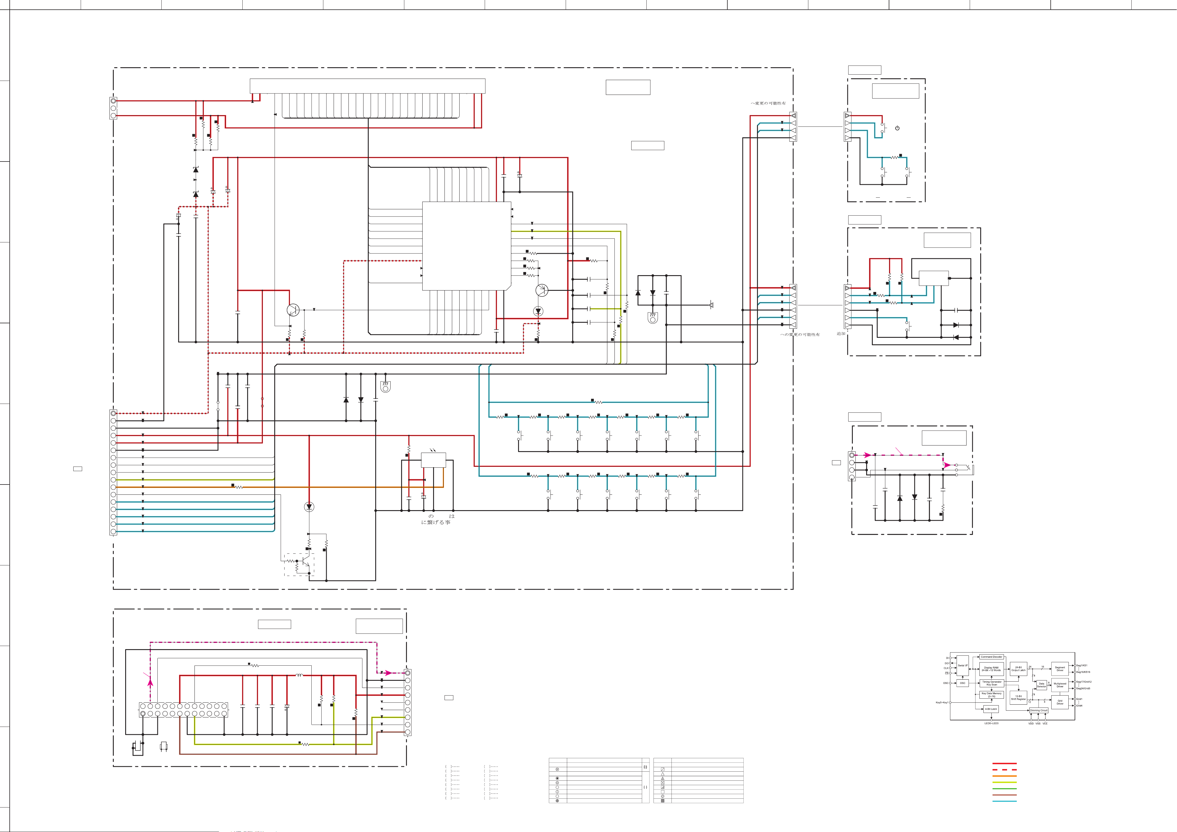
A
R-S202/R-S202D
NMLKJIHGFEDCB
1
MAIN 2/2
MAIN (3)
010ST027GNKV501
NP
F1
P13
P14
SEG4
SEG3
17
Grid4
Grid3
G4
1245678910111213141516171819202122232425262728293132
F1
P15
SEG2
16
Grid2
G2
P16
15
SEG1
Vdd
14
Vdd
Grid1
C515
13
C516
Vss
12
Vss
0.1/16
C517
0.1/16
KEY1
KEY0
STB
CLK
DMOSI
DMISO
OSC
LED3
LED2
LED1
12345678910 11
47/16
R516
R548 1.2K
R549
no_use
no_use
R550
2N5401S-RTK/P
BT LED
D514
R554
100K
Q504
–22.8V
no_use
HLMP-NS30-J0000
R517
10K
C523
100P(SL)
C518
100P(SL)
C519
100P(SL)
C520
100P(SL)
R547
CB502
to POWER
TRANSFORMER
2
PHL
3
–22V
F2
F1
–22V
F2
F2
–21.2V
1G
NP
2G
G2
270
R502
270
R501
270
R504
270
R503
3.27V
3G
G3
4G
G4
5G
6G
G6
8G
7G
G7G8G8
9G
G9
10G
G10
P16
P16
P15
P15
P14
P14
P13
P13
P11
P12
P12G5P11
D502
UDZV2.4B
–23.2V
C506
–25.3V
D501
C 5 0 4
UDZV2.4B
47/35
4 7 / 3 5
P7
P6
C501
C 5 0 3
47/35
0 . 0 1 (B )
C502
0.1/16
P5
P4
P3
P2
P1
P10
P10
P9
P8
P7
P7
P8
SEG10
SEG11
SEG12
SEG13
SEG14
SEG15
SEG16
P4
P5
P6
P6P5P4
P9
P8
SEG8
SEG9
22
2324252627282930313233
P1
P2
P2
P1
P3
P11
P12
SEG5
SEG7
SEG6
18
19
20
21
IC501
HT16515-44LQFP
Vee
SEG17
FL DRIVER
SEG18
4
G10
Q502
C508
0.1/16
C2412K(Q/R/S)
R508
R509
100K
100K
Grid10
3435363738394041424344
Grid6
Grid8
Grid7 P3
Grid9
G9
G7 P10
Grid5
G5P9G3
G6
470
R524
FL
R525
470
R528
470
MAIN (2)
D509
D510
no_use
470
G502
no_use
SPAB
VI87820
W502A
3.3M
MP_SW
SW_SPAB
120mm
MG
W503A
SAN-SAN
C521
no_use
0.1/16
to chassis
W501
1P 100MM BLACK
VOL_RA
VOL_RB
SW_PDRT
3.27V
1
0V
2
3.25V
3
0V
4
3.26V
5
0V
6
VI87840
3.27V
0V
3.27V
0V
W502B
SAN-SAN
3.3M
1
MP_SW
2
SW_SPAB
3
MG
4
SW514
<POWER>
R541
15K
AB
SW515
A
SPEAKERS
SPEAKERS
MAIN (4)
VOLUME
VOL_ENCODER
1
2
3
4
5
6
W503B
+3.3M
VOL_RA
VOL_RB
MG
SW_PDRT
FG
SAN-SAN
R701
10K
R702
R703
10K
47K
(Power)
SW516
B
REB161(9X7)PVB2
47K
R704
SW701
no_use
701-
SW702
VOL
COMBA
C701
0.1/16
D701
no_use
D702
no_use
5
F L_MISO
F L_STB
F L_MOSI
F L_SCK
G501
KEY0
KEY1
SW_PDRT
SW_SPAB
R505
no_use
R514
7.5K
<DIMMER>
R521
4.7K
SW501
R546
4 .7K
<MEMORY>
R522
3.3K
SW502
R523
3.3K
<FM/AM>
R526
2.2K
SW504
R527
2.2K
<
R529
1.5K
SW506
PRESET
R530
1.5K
R531
1K
SW508
>
R532
1K
<<
R533
1K
SW510
TUNING
R534
1K
>>
SW512
Page 45 L9
to MAIN (1)_W102
MAIN (6)
CB401
40mV
0V
0V
40mV
HPL
HPE
HPR
HP OUT L
HP
JK401
L
R
GND
JY-6317Y-03-030
PHONES
PHL
C402
SW503
SW505
SW507
SW509
SW511
SW513
0.01/100
D401
no_use
D402
no_use
C401
BASS
+
TREBLE
+
<<
INPUT
>>
0.01/100
C403
C404
no_use
R401
0.01/100
no_use
0.1/16
no_use
Remote control
sensor
SIR8430MH6
47
R513
C513
U501
GND
VCC
3.23V
C514
10/16
0.1/16
U501 BODY
MG
VOUT
3.21V
C505
CB501
52044
-VP
1
VPE
2
MG
3
+3.3M
4
+3.3S
6
Page 45 C1
to MAIN (1)_CB204
7
5
MG
6
FL_MISO
7
FL_STB
8
FL_MOSI
9
FL_SCK
10
REM
11
PLED
12
13
14
15
16
17
MPSW
KEY0
KEY1
VOL_RA
VOL_RB
to FUNC(2)
–25.3V
0V
0V
3.27V
3.27V
0V
0V
3.26V
0V
3.26V
3.22V
3.22V
0V
3.27V
3.27V
3.25V
0V
J501
no_use
C509
0.1/16
C507
0.1/16
R544
100
0.1/16
J505
FL_MISO
FL_STB
FL_MOSI
FL_SCK
MP_SW
KEY0
KEY1
VOL_RA
VOL_RB
D511
1.37V
D508
C512
no_use
D506
no_use
HLMP-Y701-G0000
L shape
FFC connector
R542
Q503
R543
1.3K
620
STANDBY/ON
indicator
DTC014EUBTL
8
MAIN (8) (R-S202D)
R603
DAB IN
L601
9
NC
AUD_L
AUD_R
NC
NC
3.3V
NC
SDA
NC
NC
NC
NC
2
4
6
8
10
12
14
16
18
20
22
24
1
3
5
7
9
11
13
15
17
19
21
NC
NC
CB601
GND
NC
GND
NC
NC
GND
SCL
NC
C601
23
GND
C602
C603
C604
N_RST
ST602
R606
R604
R605
DAB
R602
CB602
Lch
GND
Rch
3.3V
NC
NC
SCL
SDA
N_RST
Page 45 A5
to MAIN (1)_CB202
IC501: HT16515-44LQFP
1/4 to 1/12 Duty VFD controller
7
6
8
9
5
10,11
1
4-
14-29
31-38
39-42
1
44,2134,3
30
10
46
ST601
NOTICE
JAPAN
J
U.S.A
U
CANADA
C
GENERAL
R
CHINA
T
KOREA
K
AUSTRALIA
A
B BRITISH
(model)
G
L
V TAIWAN
F RUSSIAN
P LATIN AMERICA
S BRAZIL
H THAI
EUROPEAN STANDARD
SINGAPORE
SOUTH EUROPEE
CAPACITOR
REMARKS
NONOMARK
MARK
P
ELECTROLYTIC CAPACITOR
SOLID ELECTROLYTIC CAPACITOR
CERAMICCAPACITOR
POLYESTERFILMCAPACITOR
POLYSTYRENEFILMCAPACITOR
MICA CAPACITOR
POLYPROPYLENEFILMCAPACITOR
SEMICONDUCTIVE CERAMIC CAPACITOR
PARTSNAME
TUBULARCAPACITORCERAMIC
RESISTOR
REMARKS
NO MARK
PARTS NAME
CARBON
FILM RESISTOR
CARBON
FILM RESISTOR
METAL
OXIDE F ILM RESISTOR
METAL
FILM RESISTOR
METAL
PLATE RESISTOR
FIRE
PROOFCARBON FILM R ESISTOR
CEMENT
MOLDED RESISTOR
SEMI
VARIABLE RESISTOR
CHIP RESISTOR
(P=5)
(P=10)
★ All voltages are measured with a 10M Ω /V DC electronic voltmeter.
★ Components having special characteristics are marked ⚠ and must be replaced
with parts having specifications equal to those originally installed.
★ Schematic diagram is subject to change without notice.
Details of colored lines
Red / full line: Power supply (+)
Red /dashed line: Power supply (-)
Orange: Signal detect
Yellow: Clock
Green: Protection detect
Blue: Panel key input
Page 47

A
KJIHGFEDCB
L
NM
R-S202/R-S202D
1
SWITCH
2
3
4
SWITCH
(R model)
PRM_SW
VOLTAGE SELECTOR
5
6
110-120V 220-230V
3
2
1
SW1
SW1
SL14
6
5
4
F2
CB2CB1
CB3
Red
O range
P urple
Yellow
1
2
to POWER
3
TRANSFORMER
4
B4P7S-VH
7
8
9
10
NOTICE
JAPAN
J
U.S.A
U
CANADA
C
GENERAL
R
CHINA
T
KOREA
K
AUSTRALIA
A
B BRITISH
(model)
G
L
V TAIWAN
F RUSSIAN
P LATIN AMERICA
S BRAZIL
H THAI
EUROPEAN STANDARD
SINGAPORE
SOUTH EUROPEE
CAPACITOR
REMARKS
NONOMARK
MARK
P
ELECTROLYTIC CAPACITOR
SOLID ELECTROLYTIC CAPACITOR
CERAMICCAPACITOR
POLYESTERFILMCAPACITOR
POLYSTYRENEFILMCAPACITOR
MICA CAPACITOR
POLYPROPYLENEFILMCAPACITOR
SEMICONDUCTIVE CERAMICCAPACITOR
PARTSNAME
TUBULARCAPACITORCERAMIC
RESISTOR
REMARKS
NO MARK
CARBON
CARBON
METAL
METAL
METAL
FIRE
CEMENT
SEMI
CHIP RESISTOR
PARTSNAME
FILM RESISTOR
FILM RESISTOR
OXIDEFILMRESISTOR
FILM RESISTOR
PLATERESISTOR
PROOF CARBONFILMRESISTOR
MOLDED RESISTOR
VARIABLE RESISTOR
(P=5)
(P=10)
★ All voltages are measured with a 10M Ω /V DC electronic voltmeter.
★ Components having special characteristics are marked ⚠ and must be replaced
with parts having specifications equal to those originally installed.
★ Schematic diagram is subject to change without notice.
Details of colored lines
Red / full line: Power supply (+)
Red /dashed line: Power supply (-)
Orange: Signal detect
Yellow: Clock
Green: Protection detect
Blue: Panel key input
47
Page 48

■ REPLACEMENT PARTS LIST
• ELECTRICAL COMPONENT PARTS
WARNING
●
Components having special characteristics are marked ⚠ and must be replaced with parts having specifications equal to those originally installed.
ABBREVIATIONS IN THIS LIST ARE AS FOLLOWS:
R-S202/R-S202D
C.A.EL.CHP : CHIP ALUMI.ELECTROLYTIC CAP
C.CE : CERAMIC CAP
C.CE.ARRAY : CERAMIC CAP ARRAY
C.CE.CHP : CHIP CERAMIC CAP
C.CE.M.CHP : CHIP MULTILAYER CERAMIC CAP
C.CE.SAFTY : RECOGNIZED CERAMIC CAP
C.CE.TUBLR : CERAMIC TUBULAR CAP
C.CE.SMI : SEMI CONDUCTIVE CERAMIC CAP
C.EL : ELECTROLYTIC CAP
C.EL.BP : BIPOLAR ELECTROLYTIC CAP
C.EL.CHP : CHIP ELECTROLYTIC CAP
C.MICA : MICA CAP
C.ML.FLM : MULTILAYER FILM CAP
C.MP : METALLIZED POLYESTER FILM CAP
C.MYLAR : MYLAR FILM CAP
C.MYLAR.ML : MULTILAYER MYLAR FILM CAP
C.NIOB.OXD : NIOBIUM OXIDE CAP
C.PAPER : PAPER CAPACITOR
C.PLS : POLYSTYRENE FILM CAP
C.PML : POLYMER MULTI-LAYER CAPACITOR
C.POL : POLYESTER FILM CAP
C.PP : POLYPROPYLENE FILM CAP
C.PP.CHP : CHIP POLYPROPYLENE FILM CAP
C.TNTL : TANTALIUM CAP
C.TNTL.CHP : CHIP TANTALIUM CAP
C.TRIM : TRIMMER CAP
CN : CONNECTOR
CN.BS.PIN : CONNECTOR,BASE PIN
CN.CANNON : CONNECTOR,CANNON
CN.DIN : CONNECTOR,DIN
CN.FLAT : CONNECTOR,FLAT CABLE
CN.FFC : CONNECTOR,FLEXIBLE FLAT CABLE
CN.HDMI : HDMI CONNECTOR
CN.PHOTO.R : PHOTO FIBER SENSOR,RECEIVED
CN.PHOTO.T : PHOTO FIBER SENSOR,TRANSMITTED
D.SCHOTTKY : SCHOTTKY BARRIER DIODE
DIODE.ARRAY : DIODE ARRAY
DIODE.BRG : DIODE BRIDGE
DIODE.CHP : CHIP DIODE
DIODE.VAR : VARACTOR DIODE
DIODE.ZENR : ZENER DIODE
DIODE.Z.CHP : CHIP ZENER DIODE
DIODE.PHOT : PHOTO DIODE
FER.BEAD : FERRITE BEADS
FER.CORE : FERRITE CORE
FET.CHP : CHIP FET
FL.DSPLY : FLUORESCENT DISPLAY
FLTR.CE : CERAMIC FILTER
FLTR.COMB : COMB FILTER MODULE
FLTR.LC.RF : LC FILTER,EMI
FUSE.CHP : CHIP FUSE
GND.MTL : GROUND PLATE
GND.TERM : GROUND TERMINAL
JUMPER.CN : JUMPER CONNECTOR
JUMPER.TST : JUMPER,TEST POINT
L.DTCT : LIGHT DETECTING MODULE
LED.CHP : CHIP LED
LED.DSPLY : LED DISPLAY
LED.INFRD : LED,INFRARED
PHOT.CPL : PHOTO COUPLER
PHOT.INTR : PHOTO INTERRUPTER
PHOT.RFLCT : PHOTO REFLECTOR
PHOT.TR : PHOTO TRANSISTOR
PIN.TEST : PIN,TEST POINT
PTC.THERM :
R.ANTI.SURGE : FIXED ANTI SURGE RESISTOR
R.ARRAY : RESISTOR ARRAY
R.CAR. : CARBON RESISTOR
R.CAR.CHP : CHIP RESISTOR
R.CAR.FP : FLAME PROOF CARBON RESISTOR
R.CEMENT : CEMENT RESISTOR
R.CHP : CHIP RESISTOR
R.FUS : FUSIBLE RESISTOR
R.MTL.CHP : CHIP METAL FILM RESISTOR
R.MTL.FLM : METAL FILM RESISTOR
R.MTL.OXD : METAL OXIDE FILM RESISTOR
R.MTL.PLAT : METAL PLATE RESISTOR
RSNR.CE : CERAMIC RESONATOR
RSNR.CRYS : CRYSTAL RESONATOR
SCR.BND.HD : BIND HEAD B-TIGHT SCREW
SCR.TERM : SCREW TERMINAL
SCR.TR : SCREW,TRANSISTOR
SURG.PRTCT : SURGE PROTECTOR
SUPRT.PCB : P.C.B. SUPPORT
SW.LEVER : LEVER SWITCH
SW.MICRO : MICRO SWITCH
SW.LEAF : LEAF SWITCH
SW.PUSH : PUSH SWITCH
SW.RT : ROTARY SWITCH
SW.RT.ENC : ROTARY ENCODER
SW.RT.MTR : ROTARY SWITCH WITH MOTOR
SW.SLIDE : SLIDE SWITCH
SW.TACT : TACT SWITCH
TERM.SP : SPEAKER TERMINAL
TERM.WRAP : WRAPPING TERMINAL
THRMST.CHP : CHIP THERMISTOR
TR : TRANSISTOR
TR.CHP : CHIP TRANSISTOR
TR.DGT : DIGITAL TRANSISTOR
TR.DGT.CHP : CHIP DIGITAL TRANSISTOR
TR.PAIR : PAIR TRANSISTOR
TRANS : TRANSFORMER
TRANS.PULS : PULSE TRANSFORMER
TRANS.PWR : POWER TRANSFORMER
VARISTOR.C : CHIP VARISTOR
VOLT.SELCT : VOLTAGE SELECTOR
VR : ROTARY POTENTIOMETER
VR.MTR : POTENTIOMETER WITH MOTOR
VR.SLIDE : SLIDE POTENTIOMETER
VR.SW : POTENTIOMETER WITH SWITCH
VR.TRIM : TRIMMER POTENTIOMETER
POSITIVE TEMPERATURE COEFFICIENT THERMISTOR
R-S202/R-S202D
49
Page 49

R-S202/R-S202D
R-S202
MAIN
Ref No.
* ZU625400 P.C.B. MAIN UC
* ZU625500 P.C.B. MAIN R
* ZU625600 P.C.B. MAIN TK
* ZU625700 P.C.B. MAIN A
* ZU625800 P.C.B. MAIN G
* ZU625900 P.C.B. MAIN L
CB4 VG879900 CN.BS.PIN 2P
⚠
CB5-6 WN103000 CLIP.FUSE TP00351-31
⚠
CB7 VG879900 CN.BS.PIN 2P
⚠
CB101 VB389900 CN.BS.PIN 3P
* CB102 WG033601 CN.BS.PIN 52806 15P TE
* CB103 LB932031 CN.BS.PIN 3P
CB201 VQ044400 CN.BS.PIN 9P
CB202 VQ047200 CN.BS.PIN 9P
CB204 VM973500 CN.BS.PIN 17P
CB401 VB858300 CN.BS.PIN 4P
CB501 VF982300 CN.BS.PIN 17P
CB502 VB858200 CN.BS.PIN 3P
C1 UR828470 C.EL 470uF 10V
* C2-3 WJ590701 C.CE.CHP 0.47 16V K RECT.
C4 US035100 C.CE.CHP 0.1uF 16V B
C6 WQ939401 C.CE.SAFTY 0.01uF 250V
⚠
* C7 UR849221 C.EL 2200uF 25V
C8 WW194100 C.MYLAR 0.1uF 100V
C9 US063100 C.CE.CHP 1000pF 50V B
C10 UR867100 C.EL 10uF 50V R
C11 WW194100 C.MYLAR 0.1uF 100V R
C12 US063100 C.CE.CHP 1000pF 50V B
C13 WW194100 C.MYLAR 0.1uF 100V R
C14 UR866100 C.EL 1uF 50V R
C15-16 UR866100 C.EL 1uF 50V
C17 UR866220 C.EL 2.2uF 50V
C101-102 US061470 C.CE.CHP 47pF 50V B
C103-104 UR867100 C.EL 10uF 50V
C105 UR818220 C.EL 220uF 6.3V
C106 US062100 C.CE.CHP 100pF 50V B
C107-109 ZD517600 C.MYLAR 100pF 100V
C110-111 UR838100 C.EL 100uF 16V
C112-113 US060500 C.CE.CHP 5pF 50V B
C114 US062150 C.CE.CHP 150pF 50V B
C117-119 US062150 C.CE.CHP 150pF 50V B
C120 UR897470 C.EL 47uF 100V
C121-122 UR897100 C.EL 10uF 100V
C123 UR897470 C.EL 47uF 100V
C124-125 UR897100 C.EL 10uF 100V
C130 UR866220 C.EL 2.2uF 50V
C131-132 ZD520400 C.MYLAR 0.022uF 100V
C137 UR818100 C.EL 100uF 6.3V
C138 ZD517600 C.MYLAR 100pF 100V
C139 UR848330 C.EL 330uF 25V
C140 ZH987600 C.EL 6800uF 66V UCRTKAL
* C140 ZH998400 C.EL 6800uF 66V G
C141 UR867100 C.EL 10uF 50V
C142 UR867470 C.EL 47uF 50V
C143 ZH987600 C.EL 6800uF 66V UCRTKAL
R-S202/R-S202D
* C143 ZH998400 C.EL 6800uF 66V G
C144 UR829100 C.EL 1000uF 10V
C145 ZD517600 C.MYLAR 100pF 100V
C146 UR866470 C.EL 4.7uF 50V
C147 UR867100 C.EL 10uF 50V
C149 UR779100 C.EL 1000uF 63V
C150 ZD517600 C.MYLAR 100pF 100V
C152 US064100 C.CE.CHP 0.01uF 50V B
C153 UR819220 C.EL 2200uF 6.3V
C154-155 WW194100 C.MYLAR 0.1uF 100V
C157-158 WN200100 C.CE.M.CHP 0.01uF 100V TKAGL
C160-162 WN200100 C.CE.M.CHP 0.01uF 100V TKAGL
C166-167 WW194100 C.MYLAR 0.1uF 100V
Part No.
Description
Markets
Ref No.
C168-169 UR877330 C.EL 33uF 63V
C170 ZD517600 C.MYLAR 100pF 100V
C171 UR837100 C.EL 10uF 16V
C172 WW194100 C.MYLAR 0.1uF 100V
C173-176 WN200100 C.CE.M.CHP 0.01uF 100V TKAGL
C189 WN200100 C.CE.M.CHP 0.01uF 100V TKAGL
C192 US035100 C.CE.CHP 0.1uF 16V B
C193-196 US062100 C.CE.CHP 100pF 50V B
C197 UR877100 C.EL 10uF 63V
C198-199 US062100 C.CE.CHP 100pF 50V B
C204-205 US062220 C.CE.CHP 220pF 50V B
C206-207 US061470 C.CE.CHP 47pF 50V B
C208-213 US062220 C.CE.CHP 220pF 50V B
C216-217 UR837100 C.EL 10uF 16V
C230-231 UR867100 C.EL 10uF 50V
C232 US135100 C.CE.CHP 0.1uF 16V
C234-245 UR867100 C.EL 10uF 50V
C246-247 ZD519100 C.MYLAR 1800pF 100V
C248-251 UR865220 C.EL 0.22uF 50V
C252 US135100 C.CE.CHP 0.1uF 16V
C253-254 UR867100 C.EL 10uF 50V
C259-260 UR866100 C.EL 1uF 50V
C261 US135100 C.CE.CHP 0.1uF 16V
C262 UR829100 C.EL 1000uF 10V
C263-264 UR867100 C.EL 10uF 50V
C265 US063100 C.CE.CHP 1000pF 50V B
C266-267 UR866220 C.EL 2.2uF 50V
C268-270 US063100 C.CE.CHP 1000pF 50V B
C271 US135100 C.CE.CHP 0.1uF 16V
C272 US046100 C.CE.CHP 1uF 25V
C273 UR828220 C.EL 220uF 10V
C274 US062100 C.CE.CHP 100pF 50V B
C275 UR867100 C.EL 10uF 50V
C276 UR866100 C.EL 1uF 50V
C277 US135100 C.CE.CHP 0.1uF 16V
C278 UR828100 C.EL 100uF 10V
C279 US062100 C.CE.CHP 100pF 50V B
C280 US135100 C.CE.CHP 0.1uF 16V
C281 US063100 C.CE.CHP 1000pF 50V B
C282 US135100 C.CE.CHP 0.1uF 16V
C283-284 US063100 C.CE.CHP 1000pF 50V B
C285 US135100 C.CE.CHP 0.1uF 16V
C287 US135100 C.CE.CHP 0.1uF 16V
C289 US163100 C.CE.CHP 1000pF 50V
C290-291 UR837100 C.EL 10uF 16V
C292 US135100 C.CE.CHP 0.1uF 16V
C401-403 WN200100 C.CE.M.CHP 0.01uF 100V
C501 WQ711900 C.EL 47uF 35V
C502 US035100 C.CE.CHP 0.1uF 16V B
C503 US064100 C.CE.CHP 0.01uF 50V B
C504 WQ711900 C.EL 47uF 35V
C505 US035100 C.CE.CHP 0.1uF 16V B
C506 WQ711900 C.EL 47uF 35V
C507-509 US035100 C.CE.CHP 0.1uF 16V B
C512-513 US035100 C.CE.CHP 0.1uF 16V B
C514 UM397100 C.EL 10uF 16V
C515-516 US035100 C.CE.CHP 0.1uF 16V B
C517 UM397470 C.EL 47uF 16V
C518-520 US062100 C.CE.CHP 100pF 50V B
C521 US035100 C.CE.CHP 0.1uF 16V B
C523 US062100 C.CE.CHP 100pF 50V B
C701 US035100 C.CE.CHP 0.1uF 16V B
D1-4 ZP358601 DIODE 1SS352 TE
D5 WY163800 DIODE.ZENR UDZV9.1B
D6 WY164100 DIODE.ZENR UDZV12B R
D7 WH471700 DIODE.BRG DB105 1A 600V
⚠
* D8 ZU129100 DIODE.CHP F3A R
D9-10 ZP358601 DIODE 1SS352 TE
Part No.
Description
Markets
50
*
New Parts
*
New Parts
Page 50

R-S202
MAIN
R-S202/R-S202D
Ref No.
D101 WY164800 DIODE.ZENR UDZV24B
D102 ZP358601 DIODE 1SS352 TE
D103-106 ZA984400 DIODE BAV103
D107 WY162900 DIODE.ZENR UDZV3.9B
D108 WY163800 DIODE.ZENR UDZV9.1B
D109 WY164800 DIODE.ZENR UDZV24B
D110-111 ZP358601 DIODE 1SS352 TE
* D112 ZU129100 DIODE.CHP F3A
⚠
D113 VN953300 DIODE.BRG D5SBA60 5A 600V
⚠
D114 ZP358601 DIODE 1SS352 TE
D115 WY164300 DIODE.ZENR UDZV15B
D117 ZP358601 DIODE 1SS352 TE
D119-120 WY165200 DIODE.ZENR UDZV36B R
* D125-126 ZU129100 DIODE.CHP F3A
⚠
D127-128 ZP358601 DIODE 1SS352 TE
D202 WY163800 DIODE.ZENR UDZV9.1B
D203-204 WY163101 DIODE.ZENR UDZV4.7B
D207 WY163101 DIODE.ZENR UDZV4.7B
D501-502 WZ443400 DIODE.ZENR UDZV2.4B
D511 WZ745700 LED HLMP-Y701-G0000
* D514 ZR754101 LED HLMP-NS30 BLUE
F1 WQ211100 FUSE 8A 125V UCR
⚠
F1 VV071801 FUSE 4A 250V TKAGL
⚠
G101 V5995800 PLATE.GND
IC1 YD268A00 IC R1190H033B-T1-FE
⚠
IC102 XV190A00 IC NJM2904M OP AMP
IC202 YF439A00 IC BD3491FS
* IC203 YF475A00 IC.CPU R5F100JFAFA CPU unwritten
IC250 X0515B00 IC LM61CIZ THERMAL
IC501 YF471A00 IC HT16515-44LQFP
JK401 V4478300 JACK.PHONE JY-6317Y-03-030
PJ202 WD195400 JACK.PIN 6P
PJ203 WD195200 JACK.PIN 4P
Q1 WH445000 FET 3LN01C-TB-E
Q2-4 ZE933000 TR KTC4376-Y-RTF/P
Q5 ZG245700 TR KTA1661-Y-RTF/P R
⚠
Q6-7 WC397600 TR 2N5401S-RTK/P R
⚠
Q8 WC398300 TR 2N5551S-RTK/P R
Q101-104 WD896300 TR 2SA1514K R,S
Q105-106 WC292201 TR KTC3206Y-AT
Q107-108 WC883400 TR 2SD2704 K
Q109 ZG214200 TR KTD600K-Y-U/PH
⚠
Q110-111 ZG214100 TR KTB631K Y,GR
⚠
Q112 ZG214200 TR KTD600K-Y-U/PH
⚠
# Q113-116 ZU111000 TR.POWER 2SC4468 O,P,Y
⚠
Q117-118 WF549900 TR 2SC3906K T146 R,S
Q119-120 WC397600 TR 2N5401S-RTK/P
Q121 ZC256500 TR 2SC5712
* Q122 VV925403 TR.CHP 2SC2712-GR
Q123 ZE918100 TR KTA1664-Y-RTF/P
Q124 ZE933000 TR KTC4376-Y-RTF/P
Q125 WC398300 TR 2N5551S-RTK/P
Q126 WC397600 TR 2N5401S-RTK/P
Q128 WC398300 TR 2N5551S-RTK/P
Q129 ZG245700 TR KTA1661-Y-RTF/P
⚠
Q131 WC397600 TR 2N5401S-RTK/P
Q133 WC398300 TR 2N5551S-RTK/P
Q201-204 WC883400 TR 2SD2704 K
Q205-206 VV556500 TR 2SA1037K Q,R,S
Q208 WW782100 TR.DGT DTC014EUBTL
Q209 WQ381001 FET MCH6336-TL-E
Q502 VV556400 TR 2SC2412K Q,R,S
Q503 WW782100 TR.DGT DTC014EUBTL
Q504 WC397600 TR 2N5401S-RTK/P
R1 RD359220 R.CHP 2.2MΩ 1/16W J
R2 RD356100 R.CHP 1KΩ 1/16W J
R3 RD355100 R.CHP 100Ω 1/16W J
R4 RD357270 R.CHP 27KΩ 1/16W J
Part No.
Description
Markets
Ref No.
R5 RD356470 R.CHP 4.7KΩ 1/16W J
R6 RD357100 R.CHP 10KΩ 1/16W J
R7 RD357100 R.CHP 10KΩ 1/16W J R
R8 RD357100 R.CHP 10KΩ 1/16W J
* R9 WW862501 R.CAR.FP 22Ω 1/4W
R10 RD357100 R.CHP 10KΩ 1/16W J
R11 WW975700 R.MTL.OXD 47KΩ 1/4W R
R12 RD357100 R.CHP 10KΩ 1/16W J
R13 RD356330 R.CHP 3.3KΩ 1/16W J R
R14 WW975700 R.MTL.OXD 47KΩ 1/4W R
R15 RD357150 R.CHP 15KΩ 1/16W J R
R16 RD358100 R.CHP 100KΩ 1/16W J R
R17-18 RD357470 R.CHP 47KΩ 1/16W J
R101 RD356100 R.CHP 1KΩ 1/16W J
R102-103 V8071300 R.MTL.FLM 470Ω 1W
R104-105 RD357470 R.CHP 47KΩ 1/16W J
R106-107 RD356100 R.CHP 1KΩ 1/16W J
R108 RD353220 R.CHP 2.2Ω 1/16W J
R109-110 RD357330 R.CHP 33KΩ 1/16W J
R111-112 RD355820 R.CHP 820Ω 1/16W J
R113-118 RD356820 R.CHP 8.2KΩ 1/16W J
R119-120 RD356120 R.CHP 1.2KΩ 1/16W J
R121-122 RD357330 R.CHP 33KΩ 1/16W J
R123-124 RD355470 R.CHP 470Ω 1/16W J
R127-129 RD356820 R.CHP 8.2KΩ 1/16W J
R130-131 RD355120 R.CHP 120Ω 1/16W J
R132-134 RD356820 R.CHP 8.2KΩ 1/16W J
R135-136 WW865700 R.CAR.FP 5.6KΩ 1/4W
* R137-138 WW865102 R.CAR.FP 2.2KΩ 1/4W
* R139 WW863301 R.CAR.FP 100Ω 1/4W
⚠
* R140-141 WW863901 R.CAR.FP 330Ω 1/4W
* R142 WW863301 R.CAR.FP 100Ω 1/4W
⚠
R143-146 WW861300 R.CAR.FP 2.2Ω 1/4W
⚠
R147-148 ZG861500 R.WW 0.1Ω 2W
⚠
R149-150 RD355510 R.CHP 510Ω 1/16W J
R151 RD358330 R.CHP 330KΩ 1/16W J
R152-153 RD357150 R.CHP 15KΩ 1/16W J
R154 RD358330 R.CHP 330KΩ 1/16W J
R155-157 RD357470 R.CHP 47KΩ 1/16W J
R158 RD357100 R.CHP 10KΩ 1/16W J
R159-160 V8070300 R.MTL.FLM 10Ω 1W
R161 RD357470 R.CHP 47KΩ 1/16W J
R162-163 WW862101 R.CAR.FP 10Ω 1/4W
R164 RD357470 R.CHP 47KΩ 1/16W J
R165 RD357560 R.CHP 56KΩ 1/16W J
R167 RD357180 R.CHP 18KΩ 1/16W J
⚠
* R168 WW863301 R.CAR.FP 100Ω 1/4W
⚠
* R169 WW864101 R.CAR.FP 470Ω 1/4W
⚠
R170 WW863701 R.CAR.FP 220Ω 1/4W
R171-173 RD356470 R.CHP 4.7KΩ 1/16W J
R174 RD355100 R.CHP 100Ω 1/16W J
* R175 WW863301 R.CAR.FP 100Ω 1/4W
R176 RD355100 R.CHP 100Ω 1/16W J
R177 RD357470 R.CHP 47KΩ 1/16W J
R178 WW864600 R.CAR.FP 1KΩ 1/4W
⚠
* R179 WW865102 R.CAR.FP 2.2KΩ 1/4W
R180 V8070700 R.MTL.FLM 47Ω 1W
⚠
R181 RF355680 R.MTL.CHP 680Ω 1/16W D
R182 RD357470 R.CHP 47KΩ 1/16W J
R183 RD357100 R.CHP 10KΩ 1/16W J
R184 RF355680 R.MTL.CHP 680Ω 1/16W D
R185 RD357470 R.CHP 47KΩ 1/16W J
* R186 WW863901 R.CAR.FP 330Ω 1/4W UCTKAG
R186 WW863200 R.CAR.FP 82Ω 1/4W RL
R187 WW865200 R.CAR.FP 2.4KΩ 1/4W
R188-189 RD357300 R.CHP 30KΩ 1/16W J
R190 RD356330 R.CHP 3.3KΩ 1/16W J
* R191 WW863901 R.CAR.FP 330Ω 1/4W UCTKAG
Part No.
Description
Markets
R-S202/R-S202D
*
New Parts
Note:
Those parts marked with “#” are not
included in the P.C.B. assembly.
*
New Parts
51
Page 51

R-S202/R-S202D
R-S202
Ref No.
R191 WW863200 R.CAR.FP 82Ω 1/4W RL
R192 WW975500 R.MTL.OXD 39KΩ 1/4w
R193 RD357300 R.CHP 30KΩ 1/16W J
R194 RD357220 R.CHP 22KΩ 1/16W J
R195 HL006150 R.MTL.OXD 1.5KΩ 1/2W
* R196 WW863901 R.CAR.FP 330Ω 1/4W UCTKAG
R196 WW863200 R.CAR.FP 82Ω 1/4W RL
R197 RD357100 R.CHP 10KΩ 1/16W J R
R198-199 RD358470 R.CHP 470KΩ 1/16W J
R200 RD357620 R.CHP 62KΩ 1/16W J
R201 RF456100 R.CHP 1.0KΩ 1/16W F
R202 RD355470 R.CHP 470Ω 1/16W J
R203-204 RD356100 R.CHP 1KΩ 1/16W J
R205-207 RD355470 R.CHP 470Ω 1/16W J
R208-209 RD350000 R.CHP 0Ω 1/16W J
R210-211 RD358100 R.CHP 100KΩ 1/16W J
R212-215 RD355470 R.CHP 470Ω 1/16W J
R216-219 RD358470 R.CHP 470KΩ 1/16W J
R220-221 WW861600 R.CAR.FP 3.9Ω 1/4W
⚠
R222-223 RD358470 R.CHP 470KΩ 1/16W J
R224-225 RD357100 R.CHP 10KΩ 1/16W J
R226-227 RD358470 R.CHP 470KΩ 1/16W J
R228 RD353220 R.CHP 2.2Ω 1/16W J
R231 RD356100 R.CHP 1KΩ 1/16W J
R233 RD356220 R.CHP 2.2KΩ 1/16W J
R234 V8070700 R.MTL.FLM 47Ω 1W
⚠
R236-237 RD357100 R.CHP 10KΩ 1/16W J
R238 WW862101 R.CAR.FP 10Ω 1/4W
R248 RD355100 R.CHP 100Ω 1/16W J
R249 RD356100 R.CHP 1KΩ 1/16W J
* R251 RF357151 R.MTL.CHP 15KΩ 1/16W D
R252-253 RD356470 R.CHP 4.7KΩ 1/16W J
R254-255 RD356120 R.CHP 1.2KΩ 1/16W J
R256-258 RD357100 R.CHP 10KΩ 1/16W J
R259 RD358100 R.CHP 100KΩ 1/16W J
R260 RD357470 R.CHP 47KΩ 1/16W J
R261 RD358100 R.CHP 100KΩ 1/16W J
R262 RD356100 R.CHP 1KΩ 1/16W J
R263 RD358470 R.CHP 470KΩ 1/16W J
R264 RD356100 R.CHP 1KΩ 1/16W J
R265 RD357100 R.CHP 10KΩ 1/16W J
R266-267 RD355100 R.CHP 100Ω 1/16W J
R268 RD358470 R.CHP 470KΩ 1/16W J
R269 RD356100 R.CHP 1KΩ 1/16W J
R270-271 RD356470 R.CHP 4.7KΩ 1/16W J
R272 RD355100 R.CHP 100Ω 1/16W J
R273 RD356120 R.CHP 1.2KΩ 1/16W J
R274-275 RD358100 R.CHP 100KΩ 1/16W J
R276 RD355100 R.CHP 100Ω 1/16W J
R277 RD356120 R.CHP 1.2KΩ 1/16W J
R281 RD357100 R.CHP 10KΩ 1/16W J
R282 RD356100 R.CHP 1KΩ 1/16W J
* R283 RF357151 R.MTL.CHP 15KΩ 1/16W D
R284 RD358100 R.CHP 100KΩ 1/16W J
R285-287 RD355100 R.CHP 100Ω 1/16W J
R-S202/R-S202D
R288 RD353220 R.CHP 2.2Ω 1/16W J
R289-290 RD356100 R.CHP 1KΩ 1/16W J
R291 RD355100 R.CHP 100Ω 1/16W J
R292 RD357100 R.CHP 10KΩ 1/16W J
R293 RD356100 R.CHP 1KΩ 1/16W J
R294-295 RD355100 R.CHP 100Ω 1/16W J
R297-299 RD355100 R.CHP 100Ω 1/16W J
R302 RD356220 R.CHP 2.2KΩ 1/16W J
R304 RD357100 R.CHP 10KΩ 1/16W J
R305-306 RD355100 R.CHP 100Ω 1/16W J
R307 RD357330 R.CHP 33KΩ 1/16W J
R308 RD358120 R.CHP 120KΩ 1/16W J
R309 RD357120 R.CHP 12KΩ 1/16W J
Part No.
Description
MAIN
Markets
SWITCH
Ref No.
R310 RD357470 R.CHP 47KΩ 1/16W J
R311 RD356100 R.CHP 1KΩ 1/16W J
R312 RD357100 R.CHP 10KΩ 1/16W J
R313 RD355100 R.CHP 100Ω 1/16W J
* R314-317 VC756301 R.MTL.OXD 10Ω 2W
⚠
R318-320 WW863800 R.CAR.FP 270Ω 1/4W
R322 RD357180 R.CHP 18KΩ 1/16W J
⚠
R323 RD357100 R.CHP 10KΩ 1/16W J
R324 RD357470 R.CHP 47KΩ 1/16W J
R325-326 RF357220 R.MTL.CHP 22KΩ 1/16W D
R327 RF355100 R.MTL.CHP 100Ω 1/16W D
* R328-329 RF357151 R.MTL.CHP 15KΩ 1/16W D
R330-331 RF357220 R.MTL.CHP 22KΩ 1/16W D
R332 RF355100 R.MTL.CHP 100Ω 1/16W D
R335-337 RD354223 R.CHP 22Ω 1/16W J
R339-340 RD355100 R.CHP 100Ω 1/16W J
R501-504 RD355270 R.CHP 270Ω 1/16W J
R508-509 RD358100 R.CHP 100KΩ 1/16W J
R513 RD354470 R.CHP 47Ω 1/16W J
R514 RD356750 R.CHP 7.5KΩ 1/16W J
R516 RD358100 R.CHP 100KΩ 1/16W J
R517 RD357100 R.CHP 10KΩ 1/16W J
R521 RD356470 R.CHP 4.7KΩ 1/16W J
R522-523 RD356330 R.CHP 3.3KΩ 1/16W J
R524-525 RD355470 R.CHP 470Ω 1/16W J
R526-527 RD356220 R.CHP 2.2KΩ 1/16W J
R528 RD355470 R.CHP 470Ω 1/16W J
R529-530 RD356150 R.CHP 1.5KΩ 1/16W J
R531-534 RD356100 R.CHP 1KΩ 1/16W J
R541 RD357150 R.CHP 15KΩ 1/16W J
R542 RD355620 R.CHP 620Ω 1/16W J
R543 RD356130 R.CHP 1.3KΩ 1/16W J
R544 RD355100 R.CHP 100Ω 1/16W J
R546 RD356470 R.CHP 4.7KΩ 1/16W J
R547 RD355470 R.CHP 470Ω 1/16W J
R548 RD356120 R.CHP 1.2KΩ 1/16W J
R555-556 RD358100 R.CHP 100KΩ 1/16W J
R701 RD357100 R.CHP 10KΩ 1/16W J
R702 RD357470 R.CHP 47KΩ 1/16W J
R703 RD357100 R.CHP 10KΩ 1/16W J
R704 RD357470 R.CHP 47KΩ 1/16W J
RY1 WQ804101 RELAY DC DLS5D1-O(M)0.25
⚠
RY101-103 ZJ359600 RELAY 981-2A-48DS-SP7
⚠
ST1 V4040500 SCR.TERM M3
ST102-103 V4040500 SCR.TERM M3
ST250 WA246200 SCR.TERM 3.5
SW501-516 WD483100 SW.TACT SKRGAAD010
SW702 WU974000 SW.RT.ENC REB161(9X7)PVB20FI
T1 YF764A00 TRANS.SUB UC
⚠
T1 YF765A00 TRANS.SUB R
⚠
T1 YF766A00 TRANS.SUB TKAGL
⚠
TE101 V9065900 TERM.SP MSP-108V-01 PBSN
TH101 V9760200 THRMST.CHP NCP18XH103J03RB
U501 WW715100 L.DTCT SIR8430MH6
* V501 ZJ559100 FL.DSPLY 010ST027GNK
CB1-2 WN103000 CLIP.FUSE TP00351-31
CB3 V9377900 CN.BS.PIN 4P
⚠
F2 VV071801 FUSE 4A 250V
⚠
SW1 WV382901 SW.SLIDE SL14
⚠
Part No.
ZG943300 FL.SPACER
WP935100 HOLDER 1P
ZN201600 P.C.B. SWITCH R
Description
Markets
52
*
New Parts
*
New Parts
Page 52

R-S202D
MAIN
R-S202/R-S202D
Ref No.
*
⚠ CB4 VG879900 CN.BS.PIN 2P
⚠ CB5-6 WN103000 CLIP.FUSE TP00351-31
⚠ CB7 VG879900 CN.BS.PIN 2P
CB101 VB389900 CN.BS.PIN 3P
*
CB102 WG033601 CN.BS.PIN 52806 15P TE
*
CB103 LB932031 CN.BS.PIN 3P
CB201 VQ044400 CN.BS.PIN 9P
CB202 VQ047200 CN.BS.PIN 9P
CB204 VM973500 CN.BS.PIN 17P
CB401 VB858300 CN.BS.PIN 4P
CB501 VF982300 CN.BS.PIN 17P
CB502 VB858200 CN.BS.PIN 3P
CB601 ZS226200 CN 24P TE SCFS852254
CB602 VQ044400 CN.BS.PIN 9P
C1 UR828470 C.EL 470uF 10V
*
C2-3 WJ590701 C.CE.CHP 0.47 16V K RECT.
C4 US035100 C.CE.CHP 0.1uF 16V B
⚠ C6 WQ939401 C.CE.SAFTY 0.01uF 250V
*
C7 UR849221 C.EL 2200uF 25V
C8 WW194100 C.MYLAR 0.1uF 100V
C9 US063100 C.CE.CHP 1000pF 50V B
C12 US063100 C.CE.CHP 1000pF 50V B
C15-16 UR866100 C.EL 1uF 50V
C17 UR866220 C.EL 2.2uF 50V
C101-102 US061470 C.CE.CHP 47pF 50V B
C103-104 UR867100 C.EL 10uF 50V
C105 UR818220 C.EL 220uF 6.3V
C106 US062100 C.CE.CHP 100pF 50V B
C107-109 ZD517600 C.MYLAR 100pF 100V
C110-111 UR838100 C.EL 100uF 16V
C112-113 US060500 C.CE.CHP 5pF 50V B
C114 US062150 C.CE.CHP 150pF 50V B
C117-119 US062150 C.CE.CHP 150pF 50V B
C120 UR897470 C.EL 47uF 100V
C121-122 UR897100 C.EL 10uF 100V
C123 UR897470 C.EL 47uF 100V
C124-125 UR897100 C.EL 10uF 100V
C130 UR866220 C.EL 2.2uF 50V
C131-132 ZD520400 C.MYLAR 0.022uF 100V
C137 UR818100 C.EL 100uF 6.3V
C138 ZD517600 C.MYLAR 100pF 100V
C139 UR848330 C.EL 330uF 25V
*
C140 ZH998400 C.EL 6800uF 66V
C141 UR867100 C.EL 10uF 50V
C142 UR867470 C.EL 47uF 50V
*
C143 ZH998400 C.EL 6800uF 66V
C144 UR829100 C.EL 1000uF 10V
C145 ZD517600 C.MYLAR 100pF 100V
C146 UR866470 C.EL 4.7uF 50V
C147 UR867100 C.EL 10uF 50V
C149 UR779100 C.EL 1000uF 63V
C150 ZD517600 C.MYLAR 100pF 100V
C152 US064100 C.CE.CHP 0.01uF 50V B
C153 UR819220 C.EL 2200uF 6.3V
C154-155 WW194100 C.MYLAR 0.1uF 100V
C157-158 WN200100 C.CE.M.CHP 0.01uF 100V
C160-162 WN200100 C.CE.M.CHP 0.01uF 100V
C166-167 WW194100 C.MYLAR 0.1uF 100V
C168-169 UR877330 C.EL 33uF 63V
C170 ZD517600 C.MYLAR 100pF 100V
C171 UR837100 C.EL 10uF 16V
Part No.
ZU626000 P.C.B. MAIN BG
Description
Markets
Ref No.
C172 WW194100 C.MYLAR 0.1uF 100V
C173-176 WN200100 C.CE.M.CHP 0.01uF 100V
C189 WN200100 C.CE.M.CHP 0.01uF 100V
C192 US035100 C.CE.CHP 0.1uF 16V B
C193-196 US062100 C.CE.CHP 100pF 50V B
C197 UR877100 C.EL 10uF 63V
C198-199 US062100 C.CE.CHP 100pF 50V B
C204-205 US062220 C.CE.CHP 220pF 50V B
C206-207 US061470 C.CE.CHP 47pF 50V B
C208-213 US062220 C.CE.CHP 220pF 50V B
C216-217 UR837100 C.EL 10uF 16V
C230-231 UR867100 C.EL 10uF 50V
C232 US135100 C.CE.CHP 0.1uF 16V
C234-245 UR867100 C.EL 10uF 50V
C246-247 ZD519100 C.MYLAR 1800pF 100V
C248-251 UR865220 C.EL 0.22uF 50V
C252 US135100 C.CE.CHP 0.1uF 16V
C253-254 UR867100 C.EL 10uF 50V
C259-260 UR866100 C.EL 1uF 50V
C261 US135100 C.CE.CHP 0.1uF 16V
C262 UR829100 C.EL 1000uF 10V
C263-264 UR867100 C.EL 10uF 50V
C265 US063100 C.CE.CHP 1000pF 50V B
C266-267 UR866220 C.EL 2.2uF 50V
C268-270 US063100 C.CE.CHP 1000pF 50V B
C271 US135100 C.CE.CHP 0.1uF 16V
C272 US046100 C.CE.CHP 1uF 25V
C273 UR828220 C.EL 220uF 10V
C274 US062100 C.CE.CHP 100pF 50V B
C275 UR867100 C.EL 10uF 50V
C276 UR866100 C.EL 1uF 50V
C277 US135100 C.CE.CHP 0.1uF 16V
C278 UR828100 C.EL 100uF 10V
C279 US062100 C.CE.CHP 100pF 50V B
C280 US135100 C.CE.CHP 0.1uF 16V
C281 US063100 C.CE.CHP 1000pF 50V B
C282 US135100 C.CE.CHP 0.1uF 16V
C283-284 US063100 C.CE.CHP 1000pF 50V B
C285 US135100 C.CE.CHP 0.1uF 16V
C287 US135100 C.CE.CHP 0.1uF 16V
C289 US163100 C.CE.CHP 1000pF 50V
C290-291 UR837100 C.EL 10uF 16V
C292 US135100 C.CE.CHP 0.1uF 16V
C401-403 WN200100 C.CE.M.CHP 0.01uF 100V
C501 WQ711900 C.EL 47uF 35V
C502 US035100 C.CE.CHP 0.1uF 16V B
C503 US064100 C.CE.CHP 0.01uF 50V B
C504 WQ711900 C.EL 47uF 35V
C505 US035100 C.CE.CHP 0.1uF 16V B
C506 WQ711900 C.EL 47uF 35V
C507-509 US035100 C.CE.CHP 0.1uF 16V B
C512-513 US035100 C.CE.CHP 0.1uF 16V B
C514 UM397100 C.EL 10uF 16V
C515-516 US035100 C.CE.CHP 0.1uF 16V B
C517 UM397470 C.EL 47uF 16V
C518-520 US062100 C.CE.CHP 100pF 50V B
C521 US035100 C.CE.CHP 0.1uF 16V B
C523 US062100 C.CE.CHP 100pF 50V B
C601 US064100 C.CE.CHP 0.01uF 50V B
C602 US035100 C.CE.CHP 0.1uF 16V B
C603 WD758300 C.CE.CHP 10uF 10V
C604 UM388330 C.EL 330uF 6.3V
Part No.
Description
Markets
R-S202/R-S202D
*
New Parts
*
New Parts
53
Page 53

R-S202/R-S202D
R-S202D
MAIN
Ref No.
C701 US035100 C.CE.CHP 0.1uF 16V B
D1-4 ZP358601 DIODE 1SS352 TE
D5 WY163800 DIODE.ZENR UDZV9.1B
⚠ D7 WH471700 DIODE.BRG DB105 1A 600V
D9-10 ZP358601 DIODE 1SS352 TE
D101 WY164800 DIODE.ZENR UDZV24B
D102 ZP358601 DIODE 1SS352 TE
D103-106 ZA984400 DIODE BAV103
D107 WY162900 DIODE.ZENR UDZV3.9B
D108 WY163800 DIODE.ZENR UDZV9.1B
D109 WY164800 DIODE.ZENR UDZV24B
D110-111 ZP358601 DIODE 1SS352 TE
*
D112 ZU129100 DIODE.CHP F3A
⚠
⚠ D113 VN953300 DIODE.BRG D5SBA60 5A 600V
D114 ZP358601 DIODE 1SS352 TE
D115 WY164300 DIODE.ZENR UDZV15B
D117 ZP358601 DIODE 1SS352 TE
*
D125-126 ZU129100 DIODE.CHP F3A
⚠
D127-128 ZP358601 DIODE 1SS352 TE
D202 WY163800 DIODE.ZENR UDZV9.1B
D203-204 WY163101 DIODE.ZENR UDZV4.7B
D207 WY163101 DIODE.ZENR UDZV4.7B
D501-502 WZ443400 DIODE.ZENR UDZV2.4B
D511 WZ745700 LED HLMP-Y701-G0000
*
D514 ZR754101 LED HLMP-NS30 BLUE
⚠ F1 VV071801 FUSE 4A 250V
G101 V5995800 PLATE.GND
⚠ IC1 YD268A00 IC R1190H033B-T1-FE
IC102 XV190A00 IC NJM2904M OP AMP
IC202 YF439A00 IC BD3491FS
*
IC203 YF475A00 IC.CPU R5F100JFAFA CPU
IC250 X0515B00 IC LM61CIZ THERMAL
IC501 YF471A00 IC HT16515-44LQFP
JK401 V4478300 JACK.PHONE JY-6317Y-03-030
PJ202 WD195400 JACK.PIN 6P
PJ203 WD195200 JACK.PIN 4P
Q1 WH445000 FET 3LN01C-TB-E
Q2-4 ZE933000 TR KTC4376-Y-RTF/P
Q101-104 WD896300 TR 2SA1514K R,S
Q105-106 WC292201 TR KTC3206Y-AT
Q107-108 WC883400 TR 2SD2704 K
⚠ Q109 ZG214200 TR KTD600K-Y-U/PH
⚠ Q110-111 ZG214100 TR KTB631K Y,GR
Q112 ZG214200 TR KTD600K-Y-U/PH
#
Q113-116 ZU111000 TR.POWER 2SC4468 O,P,Y
Q117-118 WF549900 TR 2SC3906K T146 R,S
Q119-120 WC397600 TR 2N5401S-RTK/P
Q121 ZC256500 TR 2SC5712
Q122 VJ927101 TR 2SC2712-Y(TE85R,F)
Q123 ZE918100 TR KTA1664-Y-RTF/P
R-S202/R-S202D
Q124 ZE933000 TR KTC4376-Y-RTF/P
Q125 WC398300 TR 2N5551S-RTK/P
Q126 WC397600 TR 2N5401S-RTK/P
Q128 WC398300 TR 2N5551S-RTK/P
⚠ Q129 ZG245700 TR KTA1661-Y-RTF/P
Q131 WC397600 TR 2N5401S-RTK/P
Q133 WC398300 TR 2N5551S-RTK/P
Q201-204 WC883400 TR 2SD2704 K
Q205-206 VV556500 TR 2SA1037K Q,R,S
Q208 WW782100 TR.DGT DTC014EUBTL
Q209 WQ381001 FET MCH6336-TL-E
Q502 VV556400 TR 2SC2412K Q,R,S
Part No.
Description
Markets
Ref No.
Q503 WW782100 TR.DGT DTC014EUBTL
Q504 WC397600 TR 2N5401S-RTK/P
R1 RD359220 R.CHP 2.2MΩ 1/16W J
R2 RD356100 R.CHP 1KΩ 1/16W J
R3 RD355100 R.CHP 100Ω 1/16W J
R4 RD357270 R.CHP 27KΩ 1/16W J
R5 RD356470 R.CHP 4.7KΩ 1/16W J
R6 RD357100 R.CHP 10KΩ 1/16W J
R8 RD357100 R.CHP 10KΩ 1/16W J
*
R9 WW862501 R.CAR.FP 22Ω 1/4W
R10 RD357100 R.CHP 10KΩ 1/16W J
R12 RD357100 R.CHP 10KΩ 1/16W J
R17-18 RD357470 R.CHP 47KΩ 1/16W J
R101 RD356100 R.CHP 1KΩ 1/16W J
R102-103 V8071300 R.MTL.FLM 470Ω 1W
R104-105 RD357470 R.CHP 47KΩ 1/16W J
R106-107 RD356100 R.CHP 1KΩ 1/16W J
R108 RD353220 R.CHP 2.2Ω 1/16W J
R109-110 RD357330 R.CHP 33KΩ 1/16W J
R111-112 RD355820 R.CHP 820Ω 1/16W J
R113-118 RD356820 R.CHP 8.2KΩ 1/16W J
R119-120 RD356120 R.CHP 1.2KΩ 1/16W J
R121-122 RD357330 R.CHP 33KΩ 1/16W J
R123-124 RD355470 R.CHP 470Ω 1/16W J
R127-129 RD356820 R.CHP 8.2KΩ 1/16W J
R130-131 RD355120 R.CHP 120Ω 1/16W J
R132-134 RD356820 R.CHP 8.2KΩ 1/16W J
R135-136 WW865700 R.CAR.FP 5.6KΩ 1/4W
*
R137-138 WW865102 R.CAR.FP 2.2KΩ 1/4W
*
R139 WW863301 R.CAR.FP 100Ω 1/4W
⚠
*
R140-141 WW863901 R.CAR.FP 330Ω 1/4W
*
R142 WW863301 R.CAR.FP 100Ω 1/4W
⚠ R143-146 WW861300 R.CAR.FP 2.2Ω 1/4W
⚠ R147-148 ZG861500 R.WW 0.1Ω 2W
R149-150 RD355510 R.CHP 510Ω 1/16W J
*
R151 RD358330 R.CHP 330KΩ 1/16W J
R152-153 RD357150 R.CHP 15KΩ 1/16W J
*
R154 RD358330 R.CHP 330KΩ 1/16W J
R155-157 RD357470 R.CHP 47KΩ 1/16W J
R158 RD357100 R.CHP 10KΩ 1/16W J
R159-160 V8070300 R.MTL.FLM 10Ω 1W
R161 RD357470 R.CHP 47KΩ 1/16W J
R162-163 WW862101 R.CAR.FP 10Ω 1/4W
R164 RD357470 R.CHP 47KΩ 1/16W J
R165 RD357560 R.CHP 56KΩ 1/16W J
⚠ R167 RD357180 R.CHP 18KΩ 1/16W J
*
R168 WW863301 R.CAR.FP 100Ω 1/4W
⚠
*
R169 WW864101 R.CAR.FP 470Ω 1/4W
⚠
R170 WW863701 R.CAR.FP 220Ω 1/4W
R171-173 RD356470 R.CHP 4.7KΩ 1/16W J
R174 RD355100 R.CHP 100Ω 1/16W J
*
R175 WW863301 R.CAR.FP 100Ω 1/4W
R176 RD355100 R.CHP 100Ω 1/16W J
R177 RD357470 R.CHP 47KΩ 1/16W J
⚠ R178 WW864600 R.CAR.FP 1KΩ 1/4W
*
R179 WW865102 R.CAR.FP 2.2KΩ 1/4W
⚠ R180 V8070700 R.MTL.FLM 47Ω 1W
R181 RF355680 R.MTL.CHP 680Ω 1/16W D
R182 RD357470 R.CHP 47KΩ 1/16W J
R183 RD357100 R.CHP 10KΩ 1/16W J
R184 RF355680 R.MTL.CHP 680Ω 1/16W D
R185 RD357470 R.CHP 47KΩ 1/16W J
Part No.
Description
Markets
54
*
New Parts
Note:
Those parts marked with “#” are not
included in the P.C.B. assembly.
*
New Parts
Page 54

R-S202D
MAIN
R-S202/R-S202D
Ref No.
*
R186 WW863901 R.CAR.FP 330Ω 1/4W
R187 WW865200 R.CAR.FP 2.4KΩ 1/4W
R188-189 RD357300 R.CHP 30KΩ 1/16W J
R190 RD356330 R.CHP 3.3KΩ 1/16W J
*
R191 WW863901 R.CAR.FP 330Ω 1/4W
R192 WW975500 R.MTL.OXD 39KΩ 1/4w
R193 RD357300 R.CHP 30KΩ 1/16W J
R194 RD357220 R.CHP 22KΩ 1/16W J
R195 HL006150 R.MTL.OXD 1.5KΩ 1/2W
*
R196 WW863901 R.CAR.FP 330Ω 1/4W
R198-199 RD358470 R.CHP 470KΩ 1/16W J
R200 RD357620 R.CHP 62KΩ 1/16W J
R201 RF456100 R.CHP 1.0KΩ 1/16W F
R202 RD355470 R.CHP 470Ω 1/16W J
R203-204 RD356100 R.CHP 1KΩ 1/16W J
R205-207 RD355470 R.CHP 470Ω 1/16W J
R208-209 RD350000 R.CHP 0Ω 1/16W J
R210-211 RD358100 R.CHP 100KΩ 1/16W J
R212-215 RD355470 R.CHP 470Ω 1/16W J
R216-219 RD358470 R.CHP 470KΩ 1/16W J
⚠ R220-221 WW861600 R.CAR.FP 3.9Ω 1/4W
R222-223 RD358470 R.CHP 470KΩ 1/16W J
R224-225 RD357100 R.CHP 10KΩ 1/16W J
R226-227 RD358470 R.CHP 470KΩ 1/16W J
R228 RD353220 R.CHP 2.2Ω 1/16W J
R231 RD356100 R.CHP 1KΩ 1/16W J
R233 RD356220 R.CHP 2.2KΩ 1/16W J
⚠ R234 V8070700 R.MTL.FLM 47Ω 1W
R236-237 RD357100 R.CHP 10KΩ 1/16W J
R238 WW862101 R.CAR.FP 10Ω 1/4W
R248 RD355100 R.CHP 100Ω 1/16W J
R249 RD356100 R.CHP 1KΩ 1/16W J
*
R251 RF357151 R.MTL.CHP 15KΩ 1/16W D
R252-253 RD356470 R.CHP 4.7KΩ 1/16W J
R254-255 RD356120 R.CHP 1.2KΩ 1/16W J
R256-258 RD357100 R.CHP 10KΩ 1/16W J
R259 RD358100 R.CHP 100KΩ 1/16W J
R260 RD357470 R.CHP 47KΩ 1/16W J
R261 RD358100 R.CHP 100KΩ 1/16W J
R262 RD356100 R.CHP 1KΩ 1/16W J
R263 RD358470 R.CHP 470KΩ 1/16W J
R264 RD356100 R.CHP 1KΩ 1/16W J
R265 RD357100 R.CHP 10KΩ 1/16W J
R266-267 RD355100 R.CHP 100Ω 1/16W J
R268 RD358470 R.CHP 470KΩ 1/16W J
R269 RD356100 R.CHP 1KΩ 1/16W J
R270-271 RD356470 R.CHP 4.7KΩ 1/16W J
R272 RD355100 R.CHP 100Ω 1/16W J
R273 RD356120 R.CHP 1.2KΩ 1/16W J
R274-275 RD358100 R.CHP 100KΩ 1/16W J
R276 RD355100 R.CHP 100Ω 1/16W J
R277 RD356120 R.CHP 1.2KΩ 1/16W J
R279 RD357100 R.CHP 10KΩ 1/16W J
R280 RD356470 R.CHP 4.7KΩ 1/16W J
R281 RD357100 R.CHP 10KΩ 1/16W J
R282 RD356100 R.CHP 1KΩ 1/16W J
*
R283 RF357151 R.MTL.CHP 15KΩ 1/16W D
R284 RD358100 R.CHP 100KΩ 1/16W J
R285-287 RD355100 R.CHP 100Ω 1/16W J
R288 RD353220 R.CHP 2.2Ω 1/16W J
R289-290 RD356100 R.CHP 1KΩ 1/16W J
R291 RD355100 R.CHP 100Ω 1/16W J
Part No.
Description
Markets
Ref No.
R292 RD357100 R.CHP 10KΩ 1/16W J
R293 RD356100 R.CHP 1KΩ 1/16W J
R294-295 RD355100 R.CHP 100Ω 1/16W J
R297-299 RD355100 R.CHP 100Ω 1/16W J
R302 RD356220 R.CHP 2.2KΩ 1/16W J
R305-306 RD355100 R.CHP 100Ω 1/16W J
R307 RD357330 R.CHP 33KΩ 1/16W J
R308 RD358120 R.CHP 120KΩ 1/16W J
R309 RD357120 R.CHP 12KΩ 1/16W J
R310 RD357470 R.CHP 47KΩ 1/16W J
R311 RD356100 R.CHP 1KΩ 1/16W J
R312 RD357100 R.CHP 10KΩ 1/16W J
R313 RD355100 R.CHP 100Ω 1/16W J
*
R314-317 VC756301 R.MTL.OXD 10Ω 2W
⚠
R318-320 WW863800 R.CAR.FP 270Ω 1/4W
R322 RD357180 R.CHP 18KΩ 1/16W J
R323 RD357100 R.CHP 10KΩ 1/16W J
R324 RD357470 R.CHP 47KΩ 1/16W J
R325-326 RF357220 R.MTL.CHP 22KΩ 1/16W D
R327 RF355100 R.MTL.CHP 100Ω 1/16W D
*
R328-329 RF357151 R.MTL.CHP 15KΩ 1/16W D
R330-331 RF357220 R.MTL.CHP 22KΩ 1/16W D
R332 RF355100 R.MTL.CHP 100Ω 1/16W D
R335-337 RD354223 R.CHP 22Ω 1/16W J
R339-340 RD355100 R.CHP 100Ω 1/16W J
R501-504 RD355270 R.CHP 270Ω 1/16W J
R508-509 RD358100 R.CHP 100KΩ 1/16W J
R513 RD354470 R.CHP 47Ω 1/16W J
R514 RD356750 R.CHP 7.5KΩ 1/16W J
R516 RD358100 R.CHP 100KΩ 1/16W J
R517 RD357100 R.CHP 10KΩ 1/16W J
R521 RD356470 R.CHP 4.7KΩ 1/16W J
R522-523 RD356330 R.CHP 3.3KΩ 1/16W J
R524-525 RD355470 R.CHP 470Ω 1/16W J
R526-527 RD356220 R.CHP 2.2KΩ 1/16W J
R528 RD355470 R.CHP 470Ω 1/16W J
R529-530 RD356150 R.CHP 1.5KΩ 1/16W J
R531-534 RD356100 R.CHP 1KΩ 1/16W J
R541 RD357150 R.CHP 15KΩ 1/16W J
R542 RD355620 R.CHP 620Ω 1/16W J
R543 RD356130 R.CHP 1.3KΩ 1/16W J
R544 RD355100 R.CHP 100Ω 1/16W J
R546 RD356470 R.CHP 4.7KΩ 1/16W J
R547 RD355470 R.CHP 470Ω 1/16W J
R548 RD356120 R.CHP 1.2KΩ 1/16W J
R555-556 RD358100 R.CHP 100KΩ 1/16W J
R602 RD357100 R.CHP 10KΩ 1/16W J
R603 RD350000 R.CHP 0Ω 1/16W J
R604-605 RD356470 R.CHP 4.7KΩ 1/16W J
R606 RD350000 R.CHP 0Ω 1/16W J
R701 RD357100 R.CHP 10KΩ 1/16W J
R702 RD357470 R.CHP 47KΩ 1/16W J
R703 RD357100 R.CHP 10KΩ 1/16W J
R704 RD357470 R.CHP 47KΩ 1/16W J
⚠ RY1 WQ804101 RELAY DC DLS5D1-O(M)0.25
⚠ RY101-103 ZJ359600 RELAY 981-2A-48DS-SP7
ST1 V4040500 SCR.TERM M3
ST102-103 V4040500 SCR.TERM M3
ST250 WA246200 SCR.TERM 3.5
ST601 ZR366200 SUPPORT.DA
SW501-516 WD483100 SW.TACT SKRGAAD010
SW702 WU974000 SW.RT.ENC REB161(9X7)PVB20FI
Part No.
Description
Markets
R-S202/R-S202D
*
New Parts
*
New Parts
55
Page 55

R-S202/R-S202D
R-S202D
MAIN
Ref No.
⚠ T1 YF766A00 TRANS
TE101 V9065900 TERM.SP MSP-108V-01 PBSN
TH101 V9760200 THRMST.CHP NCP18XH103J03RB
U501 WW715100 L.DTCT SIR8430MH6
*
V501 ZJ559100 FL.DSPLY 010ST027GNK
Part No.
ZG943300 FL.SPACER
WP935100 HOLDER 1P
Description
Markets
R-S202/R-S202D
*
New Parts
56
Page 56

Carbon Resistors
R-S202/R-S202D
Value 1/4W Type Part No. 1/6W Type Part No.
1.0 Ω
1.8 Ω
2.2 Ω
3.3 Ω
4.7 Ω
5.6 Ω
10 Ω
15 Ω
22 Ω
27 Ω
33 Ω
39 Ω
47 Ω
56 Ω
68 Ω
75 Ω
82 Ω
91 Ω
100 Ω
110 Ω
120 Ω
150 Ω
160 Ω
180 Ω
200 Ω
220 Ω
270 Ω
330 Ω
390 Ω
430 Ω
470 Ω
510 Ω
560 Ω
680 Ω
820 Ω
910 Ω
1.0 kΩ
1.2 kΩ
1.5 kΩ
1.8 kΩ
2.0 kΩ
2.2 kΩ
2.4 kΩ
2.7 kΩ
3.0 kΩ
3.3 kΩ
3.6 kΩ
3.9 kΩ
4.7 kΩ
5.1 kΩ
5.6 kΩ
6.8 kΩ
8.2 kΩ
9.1 kΩ
10 kΩ
: Not available
HJ35
HJ35
HJ35
HJ35
HJ35
HJ35
HF45
HJ35
HF45
HJ35
HF45
HJ35
HF45
HF45
HF45
HF45
HF45
HF45
HF45
HJ35
HF45
HF45
HJ35
HF45
HF45
HF45
HF45
HF45
HF45
HF45
HF45
HF45
HF45
HF45
HF45
HF45
HF45
HF45
HF45
HF45
HJ35
HF45
HJ35
HF45
HF45
HF45
HJ35
HF45
HF45
HF45
HF45
HF45
HF45
HF45
HF45
3100
3180
3220
3330
3470
3560
4100
4150
4220
4270
4330
4470
4470
4560
4680
4750
4820
4910
5100
5110
5120
5150
5160
5180
5200
5220
5270
5330
5390
5430
5470
5510
5560
5680
5820
5910
6100
6120
6150
6180
6200
6220
6240
6270
6300
6330
6360
6390
6470
6510
6560
6680
6820
6910
7100
HF85
HF85
HF85
HF85
HF85
HF45
HF85
HF45
HF85
HF45
HF85
HF45
HF45
HF45
HF45
HF45
HF45
HF45
HF85
HF45
HF45
HF45
HF45
HF45
HF45
HF45
HF45
HF45
HF45
HF45
HF45
HF45
HF45
HF45
HF45
HF45
HF45
HF45
HF85
HF45
HF85
HF45
HF45
HF45
HF85
HF45
HF45
HF45
HF45
HF45
HF45
HF45
HF45
3100
3220
3330
3470
3560
4100
4150
4220
4270
4330
4390
4470
4560
4680
4750
4820
4910
5100
5110
5120
5150
5180
5200
5220
5270
5330
5390
5430
5470
5510
5560
5680
5820
5910
6100
6120
6150
6180
6200
6220
6240
6270
6300
6330
6360
6390
6470
6510
6560
6680
6820
6910
7100
Value 1/4W Type Part No. 1/6W Type Part No.
11 kΩ
12 kΩ
13 kΩ
15 kΩ
18 kΩ
22 kΩ
24 kΩ
27 kΩ
30 kΩ
33 kΩ
36 kΩ
39 kΩ
47 kΩ
51 kΩ
56 kΩ
62 kΩ
68 kΩ
82 kΩ
91 kΩ
100 kΩ
110 kΩ
120 kΩ
130 kΩ
150 kΩ
180 kΩ
220 kΩ
270 kΩ
300 kΩ
330 kΩ
390 kΩ
470 kΩ
560 kΩ
680 kΩ
820 kΩ
1.0 MΩ
1.2 MΩ
1.5 MΩ
1.8 MΩ
2.2 MΩ
3.3 MΩ
3.9 MΩ
4.7 MΩ
HF45
7110
HJ35
7120
HF45
7130
HF45
7150
HF45
7180
HF45
7220
HF45
7240
HJ35
7270
HF45
7300
HF45
7330
HF45
7360
HF45
7390
HF45
7470
HF45
7510
HF45
7560
HF45
7620
HF45
7680
HF45
7820
HF45
7910
HF45
8100
HF45
8110
HF45
8120
HF45
8130
HF45
8150
HF45
8180
HJ35
8220
HF45
8270
HF45
8300
HF45
8330
HJ35
8390
HF45
8470
HJ35
8560
HJ35
8680
HJ35
8820
HF45
9100
HJ35
9120
HJ35
9150
HJ35
9180
HJ35
9220
HJ35
9330
HJ35
9390
HJ35
9470
1/4W Type
HJ35
10mm
HF45
7110
HF85
7120
HF45
7130
HF45
7150
HF45
7180
HF45
7220
HF45
7240
HF85
7270
HF45
7300
HF45
7330
HF45
7360
HF45
7390
HF45
7470
HF45
7510
HF45
7560
HF45
7620
HF45
7680
HF45
7820
HF45
7910
HF45
8100
HF45
8110
HF45
8120
HF45
8150
HF45
8180
HF85
8220
HF45
8270
HF45
8300
HF45
8330
HF85
8390
HF45
8470
HF85
8560
HF85
8680
HF85
8820
HF45
9100
HF85
9150
HF85
9180
HF85
9220
HF85
9330
HF85
9470
1/4W Type
HF45
1/6W Type
HF85
5mm
57
Page 57

R-S202/R-S202D
JIHGFEDCBA
1
2
3
• OVERALL ASSEMBLY
77
36
32 (2)
38
78
70
73
77
76
101
R model
25
52
35
79
72
1 (7)
79
51
10
76
12
1 (5)
71
3
73
35
74
4
73
73
70
1 (6)
32 (3)
1 (3)
33
202
U, C, R, L models
70
70
1 (2)
32 (1)
2
72
202
T, K, A, G models R-S202D
103
4
72
31
5
72
50
6
200
70
70
72
70
13
1 (4)
203
R-S202
102
204
72
55
205
T model
53
55
75
72
54
14
R-S202D
611180
62
79
1 (1)
35
73
200-1
7
58
72
14
(8)
1
Page 58

R-S202/R-S202D
Ref No. Part No. Description Remarks Markets
* 1 ZU625400 P.C.B. ASSEMBLY MAIN UC
* 1 ZU625500 P.C.B. ASSEMBLY MAIN R
* 1 ZU625600 P.C.B. ASSEMBLY MAIN TK
* 1 ZU625700 P.C.B. ASSEMBLY MAIN A
* 1 ZU625800 P.C.B. ASSEMBLY MAIN R-S202 G
* 1 ZU626000 P.C.B. ASSEMBLY MAIN R-S202D BG
* 1 ZU625900 P.C.B. ASSEMBLY MAIN L
* 2 ZU626100 P.C.B. ASSEMBLY BTCARD
3 ZP339600 TUNER MODULE TUNER TU-04 R-S202 UCRL
3 ZP339700 TUNER MODULE TUNER TU-04 R-S202 TKAG
4 ZN201600 P.C.B. ASSEMBLY SWITCH R
10 YF699A00 POWER TRANSFORMER UC
⚠
10 YF700A00 POWER TRANSFORMER R
⚠
10 YF702A00 POWER TRANSFORMER T
⚠
10 YF703A00 POWER TRANSFORMER KA
⚠
10 YF705A00 POWER TRANSFORMER BG
⚠
10 YF704A00 POWER TRANSFORMER L
⚠
11 ZT362800 DAB MODULE VERONA2 R-S202D BG
# 12 ZU111000 POWER TRANSISTOR 2SC4468 O,P,Y Q113-116
* 13 MF117300 FLEXIBLE FLAT CABLE 17P 300mm P=1.25
14 MF109071 FLEXIBLE FLAT CABLE 9P 70mm P=1.25
25 WY040900 POWER CABLE 1.8m UC
⚠
25 WY042500 POWER CABLE 1.8m R
⚠
25 WY042600 POWER CABLE 1.8m T
⚠
25 WY042400 POWER CABLE 1.8m K
⚠
25 WY042100 POWER CABLE 1.8m A
⚠
25 WY041100 POWER CABLE 1.8m B
⚠
25 WY041700 POWER CABLE 1.8m GL
⚠
* 31 ZU460600 FRONT PANEL R-S202 BL UC
* 31 ZU460700 FRONT PANEL R-S202 BL RTKAGL
* 31 ZU460900 FRONT PANEL R-S202D BL
* 31 ZU460800 FRONT PANEL R-S202 SI
* 31 ZU461000 FRONT PANEL R-S202D SI
32 ZG936900 BUTTON BL
32 ZG937000 BUTTON SI
33 ZH629500 KNOB VOLUME BL
33 ZH629600 KNOB VOLUME SI
* 35 ZU649100 REAR PANEL UC
* 35 ZU649200 REAR PANEL R
* 35 ZU649300 REAR PANEL R-S202 TKAGL
* 35 ZU649400 REAR PANEL R-S202D
36 ZG942200 TOP COVER BL
36 ZG942300 TOP COVER SI
* 38 ZJ666900 SSUPPORT TOP
* 50 ZU461100 WINDOW SHEET
51 VV849300 RADIATION SHEET 19x24
52 V2438700 CORD STOPPER 10P1
53 WQ664500 SUPPORT H8
54 ZG943200 CUSHION LEG
55 ZC1818i0 LEG D60/H21 Black 20x20x2 R2
61 ZS601900 PUSH RIVET P2648(B) R-S202D
62 VQ368600 PUSH RIVET P3555-B
Ref No. Part No. Description Remarks Markets
70 WE774800 BIND HEAD P-TIGHT SCREW 3x8 MFZN2W3
71 VK173200 SCREW TRANSISTOR 3x15 SP MFC2
72 WE774300 BIND HEAD B-TIGHT SCREW 3x8 MFZN2W3
73 WE774100 BIND HEAD BONDING B-T. SCREW 3x8 MFZN2B3
74 WE877900 BIND HEAD S-TIGHT SCREW 3x6 MFZN2W3 R
75 WE774600 HEXAGONAL HEAD B-TIGHT SCREW 3x18 MFZN2W3
76 ZK590300 BIND S-TIGHT SCREW 4x10 SP MFZN2W3
77 VH313200 PW HEAD S-TIGHT SCREW 4x8-10 MFNI3BL BL
77 VD069600 PW HEAD S-TIGHT SCREW 4x8-10 MFNI33 SI
78 WE200500 DISH HEAD B-TIGHT SCREW 3x6 MFNI3BL BL
78 WE200400 DISH HEAD B-TIGHT SCREW 3x6 MFNI33 SI
79 ZK590400 BIND B-TIGHT SCREW 3x8 MFZN2W3
80 WG205000 NUT 3/8 UNEF-32 R-S202D
101 WQ621800 DAMPER 2x10x310
102 V5881100 CUSHION 5x8x25
103 ZK306200 INSULATOR 4x60x0.25
ACCESSORIES
* 200 ZU492600 REMOTE CONTROL RAX33 RC7060N010008
* 200-1 ZV285900 BATTERY COVER Black 6005A001
202 ZQ304900 FM ANTENNA 1P 1.4m 1pc R-S202 UCRL
202 VQ147100 FM ANTENNA 1.4m 1pc R-S202 TKAG
203 VR248500 AM ANTENNA 1m 1pc R-S202
204 WG233200 DAB/FM ANTENNA 1.6m 1pc R-S202D
205 ZK090800 ANTENNA ISOLATOR 11D05Z59 1pc T
BATTERY R6,AA,UM-3 2pcs
SERVICE TOOLS
ZK189200 RS-232C CONVERSION ADAPTOR V5.0 without FFC
ZD896000 FLEXIBLE FLAT CABLE 9P 150mm P=1.25 SUPPORTING TAPE
*
New Parts
Finish ....... BL: Black color, SI: Silver color
Note:
Those parts marked with “#” are not included in the P.C.B. assembly.
*
New Parts
59
Page 59

R-S202/R-S202D
RAX33
13
46
79
JIHGFEDCBA
1
■ REMOTE CONTROL
SCHEMATIC DIAGRAM PANEL
KEY NO. LAYOUT KEY CODE
Key No Function Code
1 SLEEP 7A-30
3
2
3
U1 GPM6P1001A
1
PB3 PB2
2
PB4
3
PB5
4
PD0
5
PD1
6
PD2
7
PD3
8
PD4
PB1
PB0
VSS_TX
VDD
LED
VSS
PD5
16
15
14
13
VDD VCC
12
11
10
9
VCC
C1
BAT
3 V
4.7 uF/50 V
10 12
13 15
16 18
5
8
11
14
17
4 LINE 1 7A-C1
5 LINE 2 7A-19
6 LINE 3 7A-18
7 CD 7A-15
8 TUNER 7A-16
9 BAND 7A-AE
10 TUNING
11 TUNING
12 MEMORY 7F01-6718
13 PRESET 7F01-5E21
14 PRESET
15 INFO 7A-2758
STANDBY/ON 7E-2A
z
7F01-641B
7F01-611E
7F01-5B24
16 TREBLE - 7A-BAC5
19 21
124711162229374656
4
5
35812172330384757
6913 18 24 31 39 48 58
10 14 19 25 32 40 49 59
15 20 26 33 41 50 60
21 27 34 42 51 61
28 35 43 52 62
36 44 53 63
45 54 64
55 65
66
22 23
29 30
20
24
26
25 27
28
31
34
33
17 TREBLE + 7A-B9C6
18 SPEAKERS A 7A-9A
19 BASS - 7A-B8C7
20 BASS + 7A-B7C8
21 SPEAKERS B 7A-9B
22 BALANCE L 7A-BBC4
23 BALANCE R 7A-BCC3
24 ▲ (up)/BLUETOOTH 7A-9D
25
26 ENTER 7A-DE
27
28
(left)/BLUETOOTH
▲
▲
(right)/BLUETOOTH
▲
(down)/BLUETOOTH
f
g
ad
7A-9F
7A-9E
7A-9C
29 MENU 7A-84
30 DIMMER 7A-82FD
31 VOLUME + 7A-1A
33 MUTE 7A-1C
34 VOLUME - 7A-1B
37 39
6
40 42
38
41
37
38
39
(stop) 79-56
s
(pause) 79-55
d
(play) 79-02
a
40 DISC SKIP 79-4F
43 45
44
41
42
43
44
45
(skip-) 79-04
f
(skip+) 79-07
g
(open/close) 79-01
(search-) 79-05
h
(search+) 79-06
j
7
60
Page 60

MEMO
R-S202/R-S202D
R-S202/R-S202D
61
Page 61

R-S202/R-S202D
 Loading...