

Yamaha ACU-16-C Service Manual
ACU16-C
AMP CONTROL UNIT
SERVICE MANUAL
このサービスマニュアルはエコパルプ
(ECF:無塩素系漂白パルプ)を使用しています。
011673
PA
20030301-オープンプライス
CONTENTS
SPECIFICATIONS ................................................ 3/4
PANEL LAYOUT .................................... 5
DIMENSIONS ............................................................ 5
CONNECTOR WIRING ................. 6
CIRCUIT BOARD LAYOUT ................. 7
WIRING ..................................................................... 7
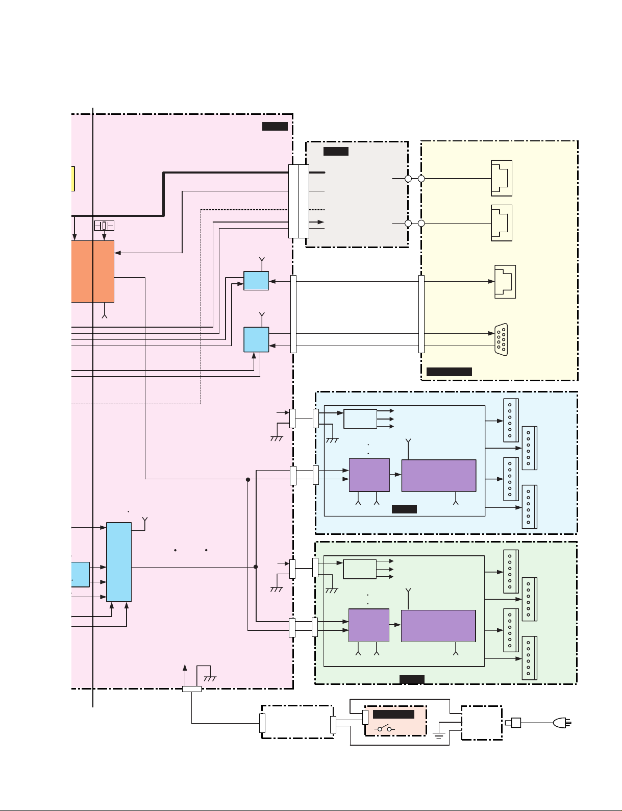
BLOCK DIAGRAM
DISASSEMBLY PROCEDURE ............................ 10
LSI PIN DESCRIPTION .............................. 13
IC BLOCK DIAGRAM ................................. 17
CIRCUIT BOARDS ....................................... 20
INSPECTIONS ...................................................... 29/31
TEST PROGRAM .............................. 33/39
OVERALL CIRCUIT DIAGRAMS
PARTS LIST
(結線図)
(目次)
(
総合仕様
(パネルレイアウト)
(
寸法図
(ブロックダイアグラム)
(ICブロック図)
(シート基板図)
(検査)
(テストプログラム)
)
)
(コネクターワイヤリング)
(ユニットレイアウト)
(分解手順)
(LSI端子機能表)
(総回路図)
0.166K-0387 Printed in Japan 2003.02
.............................. 8
HAMAMATSU, JAPAN
1
ACU16-C
IMPORTANT NOTICE
This manual has been provided for the use of authorized Yamaha Retailers and their service personnel. It has been assumed
that basic service procedures inherent to the industry, and more specifically Yamaha Products, are already known and understood by the users, and have therefore not been restated.
WARNING : Failure to follow appropriate service and safety procedures when servicing this product may result in per-
IMPORTANT : This presentation or sale of this manual to any individual or firm does not constitute authorization certifi-
The data provided is belived to be accurate and applicable to the unit(s) indicated on the cover. The research engineering, and
service departments of Yamaha are continually striving to improve Yamaha products. Modifications are, therefore, inevitable
and changes in specification are subject to change without notice or obligation to retrofit. Should any discrepancy appear to
exist, please contact the distributor’s Service Division.
WARNING : Static discharges can destroy expensive components. Discharge any static electricity your body may have
IMPORTANT : Turn the unit OFF during disassembly and parts replacement. Recheck all work before you apply power
sonal injury, destruction of expensive components and failure of the product to perform as specified. For
these reasons, we advise all Yamaha product owners that all service required should be performed by an
authorized Yamaha Retailer or the appointed service representative.
cation, recognition of any applicable technical capabilities, or establish a principal-agent relationship of
any form.
accumulated by grounding yourself to the ground bus in the unit (heavy gauge black wires connect to
this bus.)
to the unit.
WARNING: CHEMICAL CONTENT NOTICE!
The solder used in the production of this product contains LEAD. In addition, other electrical/electronic and/or plastic (Where
applicable) components may also contain traces of chemicals found by the California Health and Welfare Agency (and possibly
other entities) to cause cancer and/or birth defects or other reproductive harm.
DO NOT PLACE SOLDER, ELECTRICAL/ELECTRONIC OR PLASTIC COMPONENTS IN YOUR MOUTH FOR ANY REASON WHAT
SO EVER!
Avoid prolonged, unprotected contact between solder and your skin! When soldering, do not inhale solder fumes or expose
eyes to solder/flux vapor!
If you come in contact with solder or components located inside the enclosure of this product, wash your hands before handling
food.
WARNING: THIS APPARATUS MUST BE EARTHED
IMPORTANT
THE WIRES IN THIS MAINS LEAD ARE COLOURED IN
ACCORDANCE WITH THE FOLLOWING CODE:
GREEN-AND-YELLOW : EARTH
BLUE : NEUTRAL
BROWN : LIVE
As the colours of the wires in the mains lead of this apparatus may
not correspond with the coloured markings identifying the terminals in
your plug, proceed as follows:
The wire which is coloured GREEN and YELLOW must be
connected to the terminal in the plug which is marked by the letter E
or by the safety earth symbol or coloured GREEN and YELLOW.
The wire which is coloured BLUE must be connected to the terminal
which is marked with the letter N or coloured BLACK.
The wire which is coloured BROWN must be connected to the
terminal which is marked with the letter L or coloured RED.
* This applies only to products distributed by YAMAHA KEMBLE
MUSIC (U.K.) LTD.
WARNING
Componentshavingspecialcharacteristicsaremarkedandmustbe
replacedwithpartshavingspecificationequaltothoseoriginallyinstalled.
印の商品は、安全を維持するために重要な部品です。交換する場合は、
安全のために必ず指定の部品をご使用下さい。
2
ACU16-C
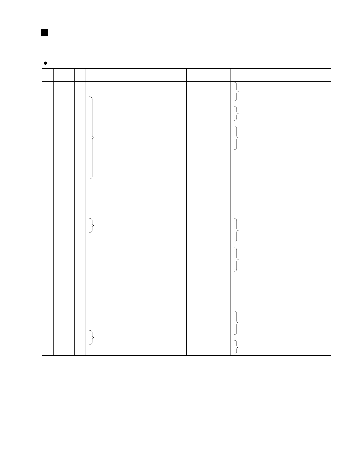
SPECIFICATIONS
D/A converters
Dynamic range
Frequency response
Crosstalk
Signal delay
Total harmonic distortion
(20 Hz–20 kHz)
Hum & noise
CobraNet
Analog out
Computer ports
Amp control RS-485
Unit ID
Power Requirements
Dimensions (W x H x D)
Net weight
Operating free-air temperature range
Storage temperature range
Supplied Accessories
1. Measured using a 6 dB/octave filter @ 12.7 kHz; equivalent to a 20 kHz filter with an infinite dB/octave attenuation.
1
1
(総合仕様)
+4 dB output
Full scale output
PRIMARY/SECONDARY
connectors
Network status
indicators
Channels
Connector
Source impedance
For use with nominal
Output level
TO COMPUTER
USB
U.S./Canada
Other
24-bit, 128-times oversampling
110 dB typical
20 Hz–20 kHz +0.5, –1.5 dB (nominal output level @ 1 kHz)
–80 dB (@ 1 kHz, between adjacent channels)
0.625 ms (CobraNet to analog output)
Less than 0.05%
Less than 0.01%
–92 dB
RJ-45 x2 (16 in), transformer isolated, IEEE 802.3
LINK, CONDUCT, ERROR LEDs
CH1–16 balanced outputs
Euro-block connectors 6-way x8
150 Ω
10k Ω lines
Nominal: +4 dB (1.23 V), Max. before clip: +18 dB (6.16 V)
9-pin male D-sub (RS-232C)
USB 1.1
RJ-45 x1
0–F (0–15)
110–120 V, 50/60 Hz, 40 W
220–240 V, 50/60 Hz, 40 W
480 x 44.65 x 385.5 mm (18 7/8" x 1 3/4" x 15 5/32"), 1U
4.8 kg (10.6 lbs)
0–40°C (32–104°F)
–20 to 60°C (–4 to 140°F)
CD-ROM (NetworkAmp Manager, PDF manual, MIDI drivers)
Power cord and retaining clamp
USB cable
3-way Euro-block connectors x16
Owner's Manual
3
ACU16-C
D/Aコンバータ 24ビット、128倍オーバーサンプリング
ダイナミックレンジ
周波数特性 20Hz〜20kHz+0.5,−1.5dB(ノミナル出力レベル@1kHz)
クロストーク −80dB(@1kHz隣接チャンネル間)
シグナルディレイ 0.625ms(CobraNet →アナログ出力)
全高調波歪
ハム、ノイズ
CobraNet
アナログ出力
PCポート
アンプコントロール RS-485 RJ-45×1
ユニットID 0〜F(0〜15)
電源 100V、50/60Hz、40W
最大外形寸法 (W ×H×D) 480×44.65×385.5mm、1U
重量 4.8kg
動作環境温度 0〜40℃
保管温度 −20〜60℃
付属品
*1
+4dB出力 0.05%
全スケール出力 0.01%
*1
PRIMARY/SECONDARY
ポート
ネットワークインジケー
ター
チャンネル CH1〜16バランス出力
コネクター 6ピン・ユーロブロックコネクター×8
ソースインピーダンス 150Ω
ノミナルレベル 10kΩライン
出力レベル ノミナル:+4dB(1.23V)、クリップ前最大:+18dB(6.16V)
TOCOMPUTER 9ピン・オスD-sub(RS-232C)
USB USB1.1
110dBtypical
−92dB
RJ-45×2(16入力)、トランスフォーマーアイソレート、IEEE802.3
LINK、CONDUCT、ERRORLED
CD-ROM(NetworkAmpManager、PDF形式取扱説明書、
MIDIドライバ)
電源コード、誤脱防止クランプ
電源プラグ変換アダプター
USBケーブル
3ピン・ユーロブロックコネクター×16
取扱説明書
*1 6dB/oct.フィルター@12.7kHz;20kHzフィルター∞ dB/oct.アッテネーションと同等
4
ACU16-C
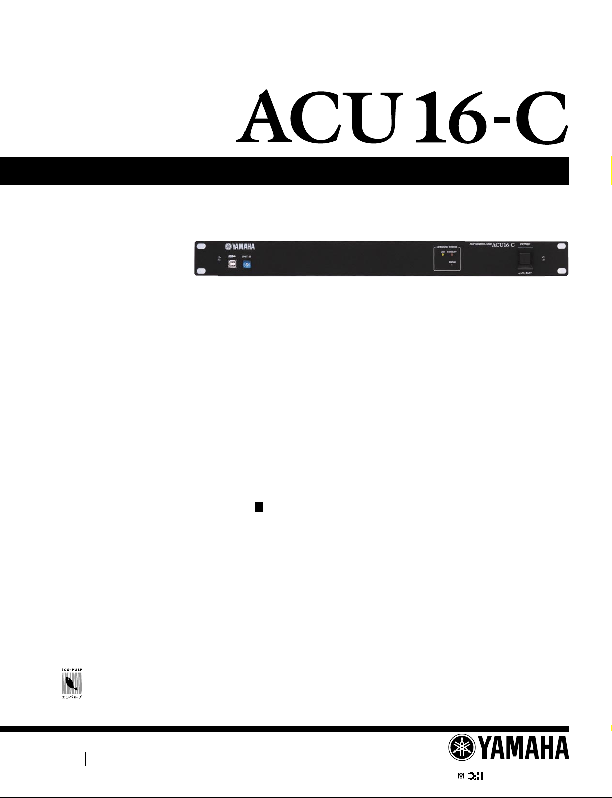
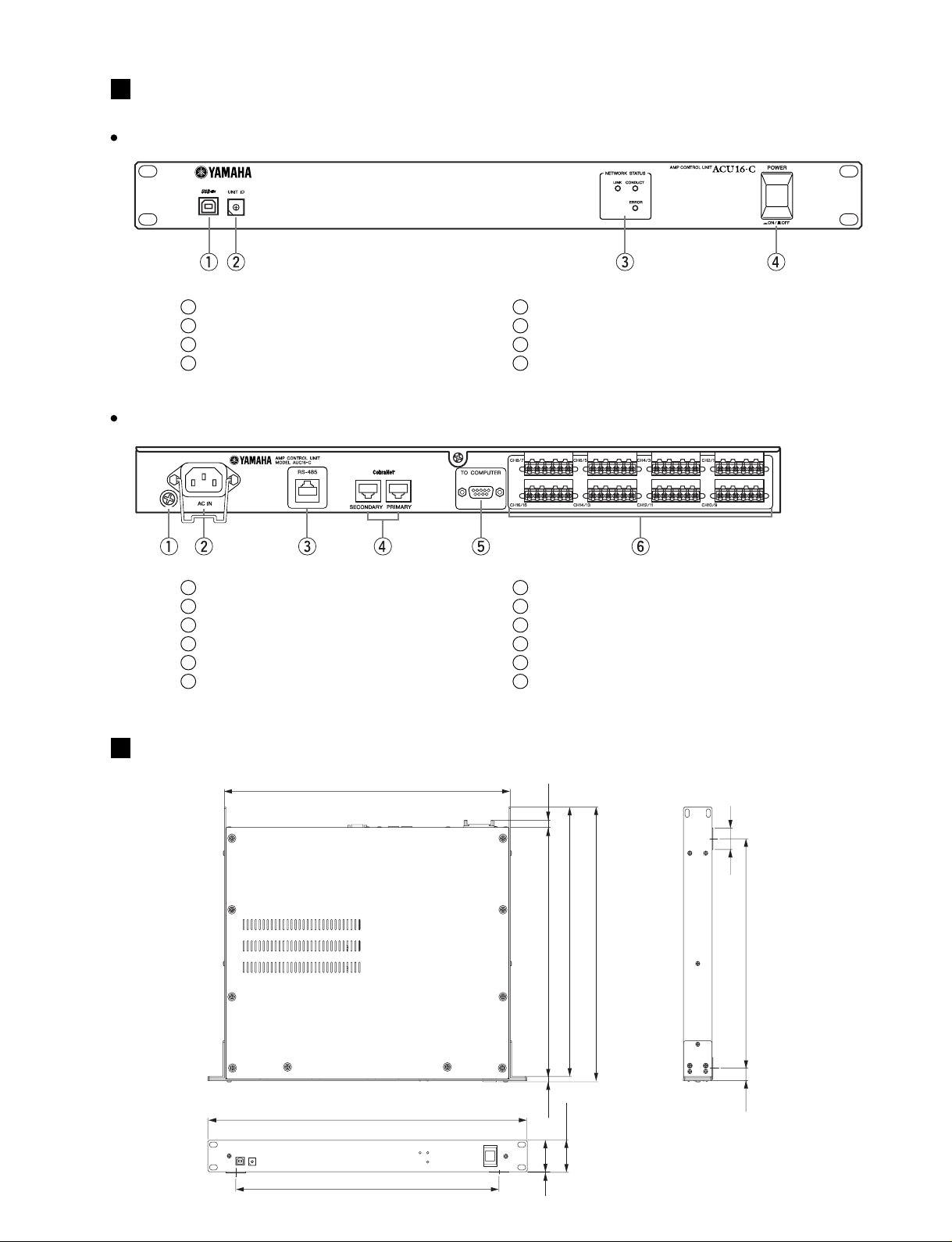
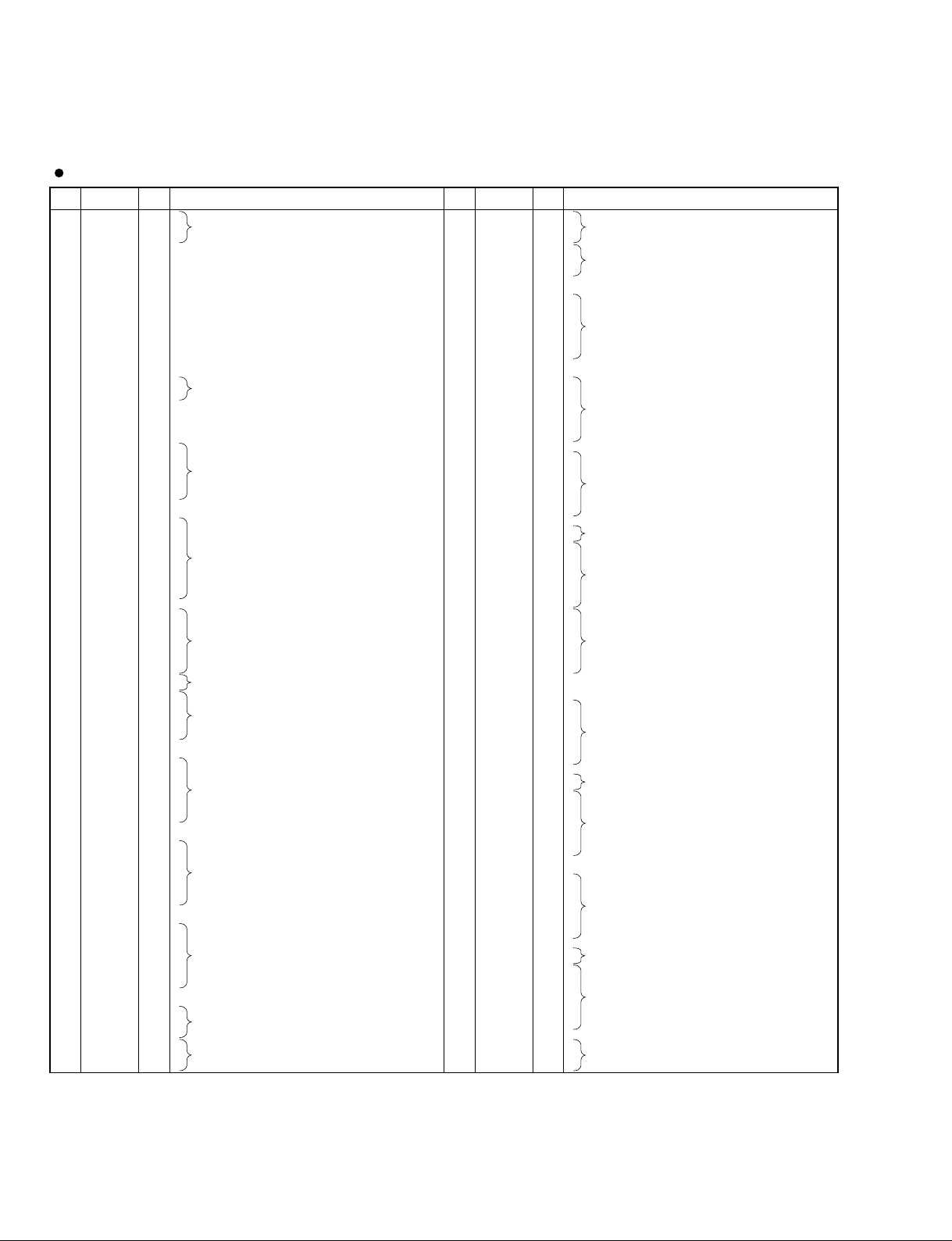
PANEL LAYOUT
Front Panel
Rear Panel
(フロントパネル)
1
USB port
2
UNIT ID switch
3
NETWORK STATUS indicators
4
POWER ON/OFF switch
(リアパネル)
(パネルレイアウト)
1
USB ポート
2
UNITID スイッチ
3
NETWORKSTATUS インジケーター
4
POWERON/OFFスイッチ
1
Grounding screw
2
AC IN connector
3
RS-485 port
4
PRIMARY & SECONDARY CobraNet ports
5
TO COMPUTER port
6
Euro-block connectors
DIMENSIONS
(寸法図)
430
1
アース用ネジ
2
ACIN ソケット
3
RS-485 ポート
4
PRIMARY/SECONDARYCobraNet ポート
5
TOCOMPUTER ポート
6
ユーロブロックコネクター
30
378
D:385.5
W:480
395.8
7.5 349.3 10.2
44
0.65
17.5 322
H:44.65
Units: mm
(単位)
5
ACU16-C
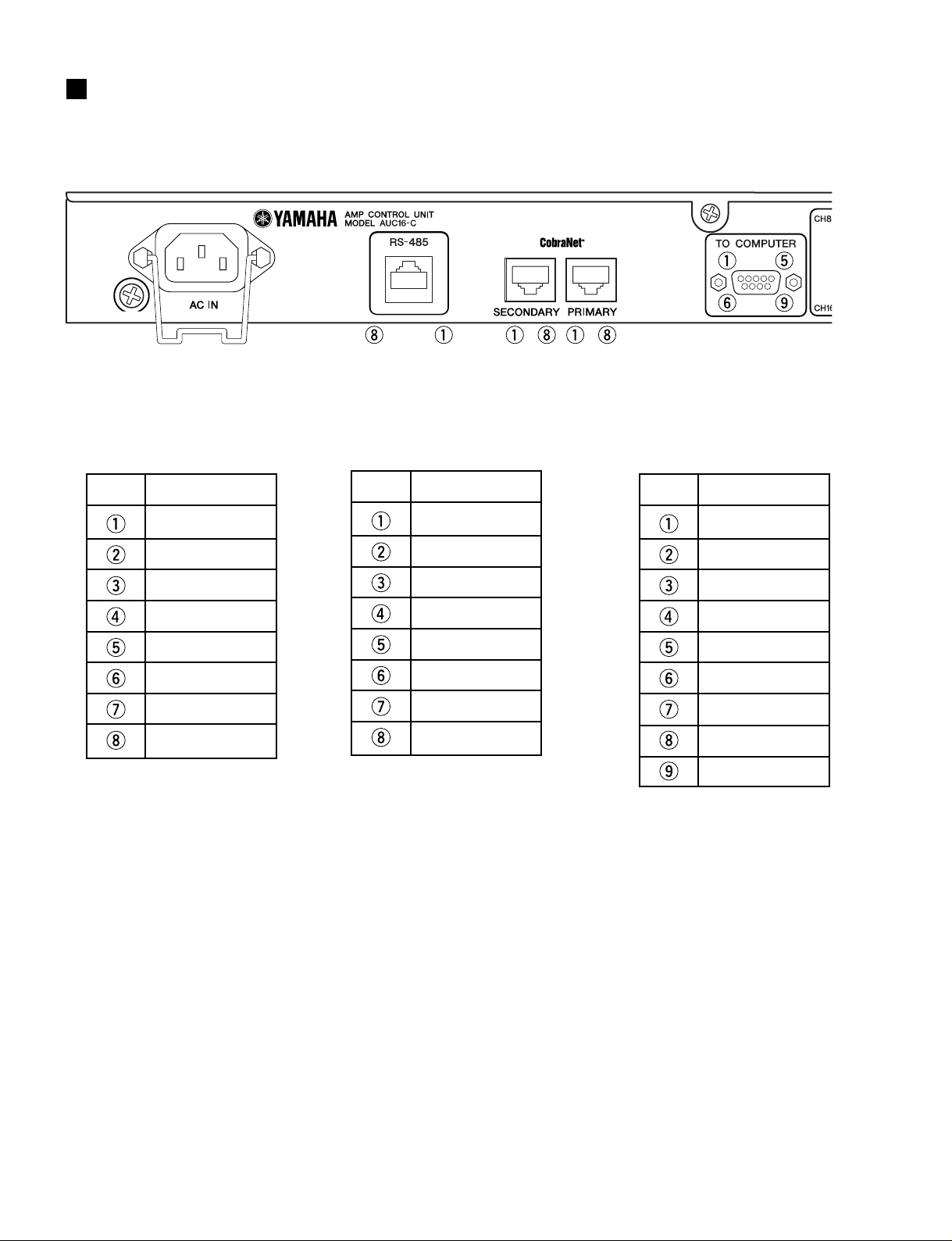
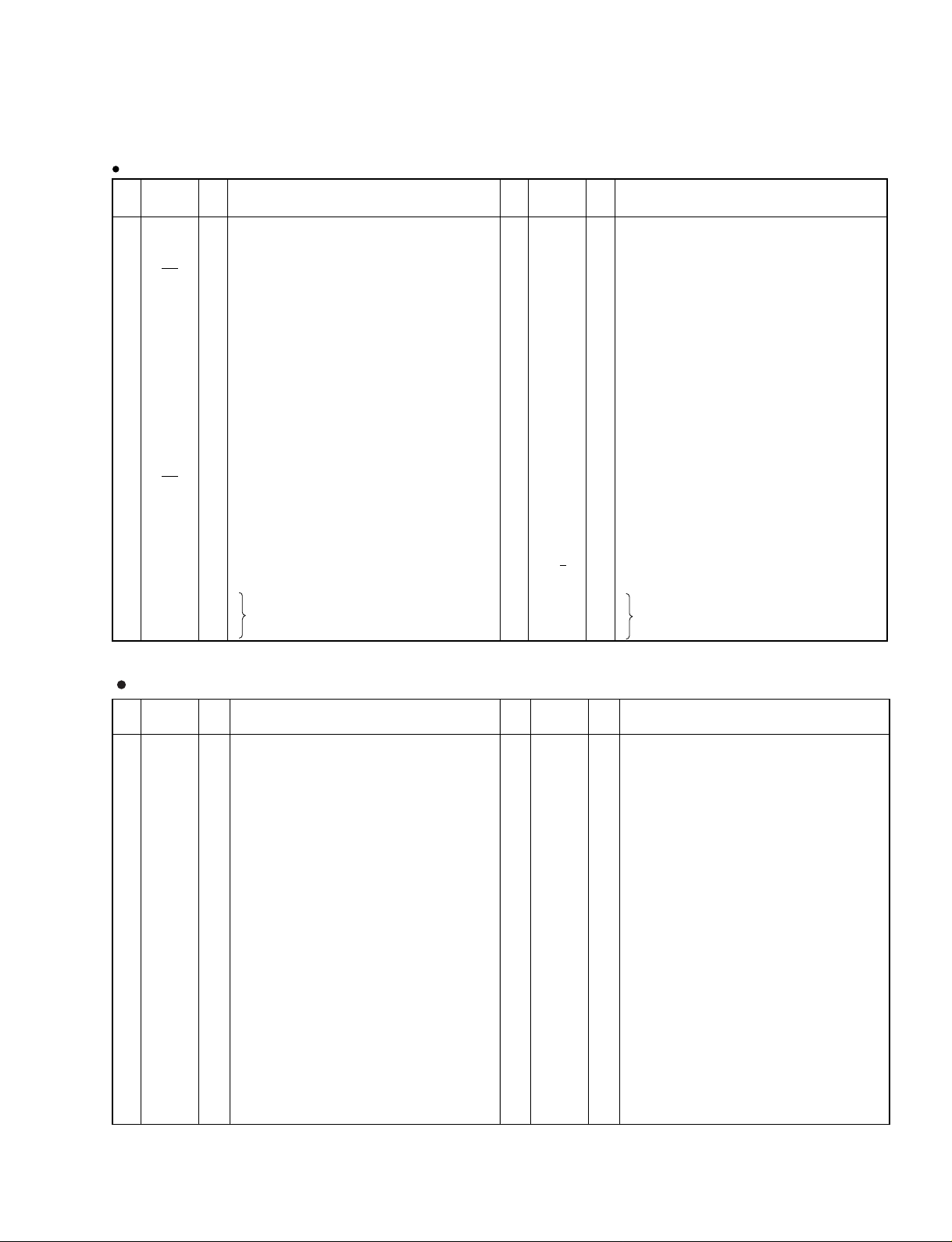
CONNECTOR WIRING
RS-485
Pin Connection
Unused
(コネクターワイヤリング)
Cobra Net
(PRIMARY, SECONDARY)
Pin Connection
TxD+
TO COMPUTER
Pin Connection
Unused
Unused
Unused
RxD/TxD+
RxD/TxDUnused
FG
FG
TxDRxD+
Unused
Unused
RxDUnused
Unused
RxD
TxD
DTR
GND
DSR
RTS
CTS
Unused
6
ACU16-C
CIRCUIT BOARD LAYOUT
DAC2
DAC1
(ユニットレイアウト)
DAC-JACK
CM-1
(電源
ユニット)
MAIN
AC INLET
POWER
UNIT
DAC-
PSW
WIRING
DAC1
CN301 (B)
to MAIN
to MAIN
CN307
(結線図)
CN201
CN603
DAC2
CN501 (B)CN501 (B) CN401CN401CN401
MAIN
MFA21060
150
CN604
CN603
CN301
CN601 (B)
CM-1
CN307
DAC-LED
DAC-JACK
CN306
CN406
140
V9703000
CN1
POWER
UNIT
(電源
ユニット)
CN51
CN203
DAC-LED
CN801 (B)
160
V9544800
DAC-
PSW
CN701
7
ACU16-C
6
5
6
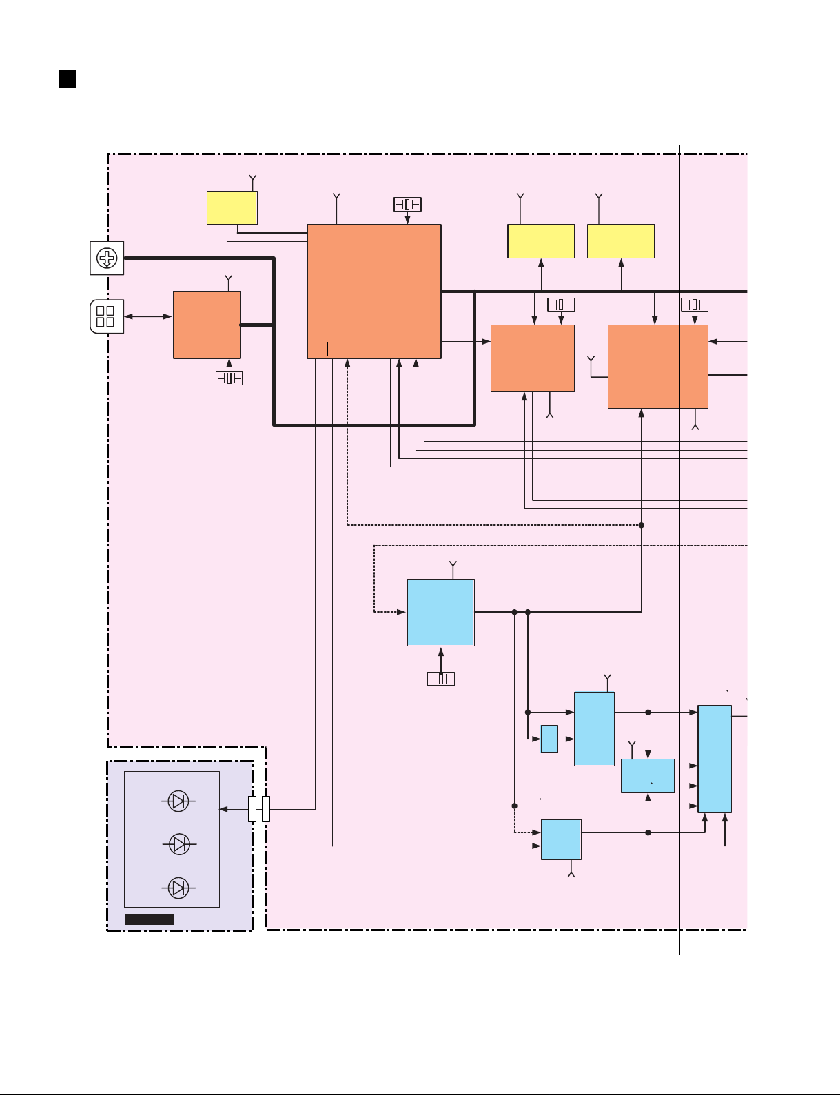
BLOCK DIAGRAM
UNIT ID
USB
SW201
8
79
62A
5
B
4C
D
3
E
1
F
0
CN308
IC316
USB CPU
M37641M8
IC221
256kbit
EEPROM
SDA
SCL
56
+5D
16, 74
XIN, OUT
14, 15
16MHz
X302
(ブロックダイアグラム)
+5D
8
104
105
IC201
PE6
PE7
+5D
21, 37, 55
77, 103, 100
VCC
MAIN CPU
SH7042A/28MHz
Ø25.8048MHz
MPU_MODE:2
RES
TIOC 18
D12-15
84
102
52~54, 56
X201
6.4512MHz
72, 74
XTAL,
EXTAL
TXD1
RXD1
RXD0
47
48
51
A0-15
CK
TXD0
50
D0-15
A: 4~20
D: 52-54, 56-60
62-64, 66-70
CKO
41
+5D
IC203 IC204
37
4Mbit
FLASH
IC301
CPU CLK
SIO4
RX2
TX2
20
21
+5D
+5D
1, 6, 21
16Mbit
DRAM
8MHz
X301
IC601
32, 34 7
XI
XO
43,19
+3.3D
174,
195
114
144
5
37
57
86
VDD
256FS
SYNC
DSP5
(MIXER)
18
A
SO0~7
VDD
96, 76, 58, 24,
20, 12, 9, 194,
173, 143, 124
+5D
60MHz
X601
67-69
115-122
LD801
LD803
LD804
LINK
CONDUCT
ERROR
CN801
6P-B
CN203
6P
FS
IC502
35
PLL &
Clock
Generater
11.727 MHz
SYNC_RES
DIR2
XI, XO
X501
+5D
12, 13
39
MASTER
Clock
8 FS
7 64FS
9 128FS
10 256FS
6 SYNC
256FS
26
x2
IC504
FS 64FS
IC510
FS
Reset
Output
2
Control
5
14
+5D
IC505
48k/96k
Master
Clock
selecter
5
6
+5D
14
3
6
+5D
Divider
IC507 508
IC506
13
132216
9
selecter
5
111
IC509
Clock
+
14
25
10,
1, 4, 1
DAC-LED
A'
8
SP5
XER)
8
A
7
SO0~7
VDD
96, 76, 58, 24,
20, 12, 9, 194,
173, 143, 124
+5D
IC506
IC509
13
60MHz
X601
67-69
115-122
ACU16-C
MAIN
CM-1
CN402,
CN403
NETIN[0~3]
40P
5P 40P
485RXD
485TXD
NET_WC
IC307
1
RS485
4
DRIVER
IC302
+5D
+5D
8
4, 16
CN301
DRIVER
15 3
TX2
RX2
CN306
(or CN307)
+5DA
CN501
4P
4P-B
DAGND
DA1~8
D1~4
+5D
14
21P
CN604
21P
CN401
(CobraNET)
POWER
SUPPLY
DAGND
IC403 IC404
IC503 IC504
AK4393
24bit D/A
Converter
+5DA
x4
218
+5A
JK601
JK602
CN601
5P-B
DAC-JACK
+12A
-12A
+5A
+12A
IC405~IC410
IC506~IC511
8
V+
Analog-Output-Circuit
DAC2
-12A
JK604
PRIMARY
CobraNet
JK605
JK603
SECONDARY
RS-485
JK602
TO COMPUTER
CH2/1
CH4/3
CH6/5
4
CH8/7
er
508
256FS_DAC FS_DAC /64FS_DAC
Clock
132
9
selecter
10, 6, 3
5
11
1, 4, 10
+D5
DGND
4P
CN406
A'
CN307
(or CN306)
+5DA
DAGND
DA5~8
CN51
4P
POWER UNIT
4P
21P
CN603
CN301
4P-B
21P
CN201
CN1
POWER
SUPPLY
DAGND
IC203 IC204
IC303 IC304
AK4393
24bit D/A
Converter
+5DA
5P
x4
218
+5A
DAC-PSW
3P
+12A
-12A
+5A
+12A
IC205~IC210
IC306~IC311
8
V+
Analog-Output-Circuit
DAC1
POWER
4
-12A
CH10/9
CH12/11
CH14/13
CH16/15
AC INLET
AC CORD
CN701
38CA1-8821493
9
ACU16-C
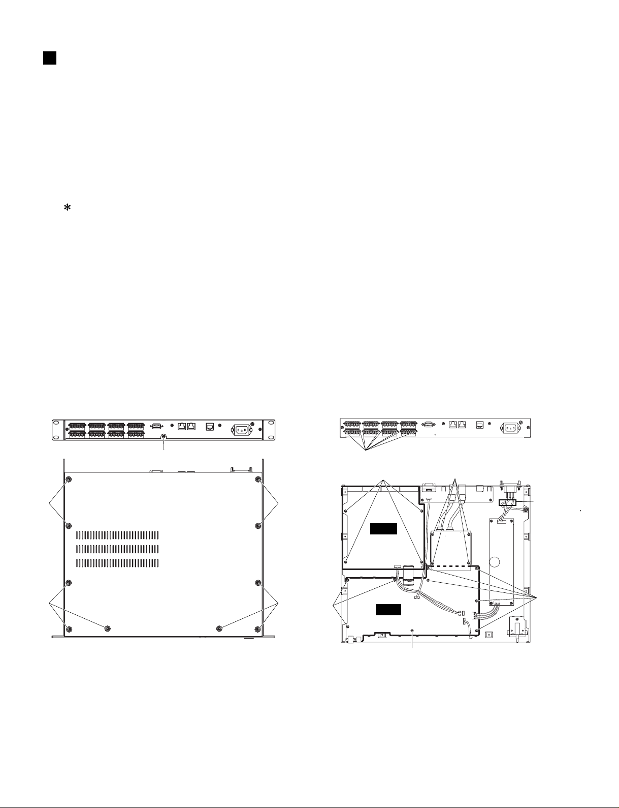
DISASSEMBLY PROCEDURE
(分解手順)
1. Top Cover (Time required: 1 minute)
1-1 Remove the eleven (11) screws marked [480]. The
top cover can then be removed. (Fig. 1)
2. CM-1 Assembly (Time required: 2 minutes)
2-1 Remove the top cover. (See Procedure 1.)
2-2 Remove the four (4) screws marked [400a]. The CM-
1 assembly can then be removed. (Fig. 2)
When removing the CM-1 assembly , use care so as
not to bend connector pins of CN402 and CN403.
3. MAIN Circuit Board (Time required: 3 minutes)
3-1 Remove the top cover. (See Procedure 1.)
3-2 Remove the CM-1 assembly. (See Procedure 2.)
3-3 Remove the nine (9) screws marked [400b]. The
MAIN circuit board can then be removed. (Fig. 2)
4. DAC2 Circuit Board (Time required: 3 minutes)
4-1 Remove the top cover. (See Procedure 1.)
4-2 Remove the f our (4) scre ws marked [490] fixing the
circuit board and eight (8) screws marked [460] from
the rear panel. The DAC2 circuit board can then be
removed. (Fig. 2)
1. トップカバー(所要時間:1 分)
1-1. ネジ[480]11本を外し、トップカバーを外します。
(Fig.1)
2. CM-1Ass'y(所要時間:2 分)
2-1. トップカバーを外します。(1 項参照)
2-2. ネジ[400a]4本を外し、CM-1Ass'y を外します。
(Fig. 2)
※CN402、403のコネクタピンを曲げない様、注意し
て外して下さい。
3. MAIN シート(所要時間:3分)
3-1. トップカバーを外します。(1 項参照)
3-2. CM1Ass'yを外します。(2 項参照)
3-3. ネジ[400b]9本を外し、MAIN シートを外します。
(Fig. 2)
4. DAC2 シート(所要時間:3分)
4-1. トップカバーを外します。(1 項参照)
4-2. シートを止めているネジ[490]4本と、リアパネルの
ネジ[460]8本を外し、DAC2シートを外します。
(Fig. 2)
[480]
[480]
[480]
[480]: Bonding Tapping Screw-S 3.0X6 MFZN2BL (V7451800)
Fig.1
[480]
[480]
ボンディングSタイト
[400]: Bind Head Tapping Screw-B 3.0X6 MFZN2BL (EP600230)
[460]: Pan Head Screw 2.6X6 MFZN2BL (VC990500)
[490]: Bind Head Tapping Screw-S 3.0X6 MFZN2BL (EP630210)
[400b]
[460]
[490]
DAC2
MAIN
[400a]
Ferrite Core
(フェライト)
CM-1
Ass'Y
[400b]
[400b]
+バインドBタイト
+ナベ小ネジ
+バインドSタイト
Fig.2
10
ACU16-C
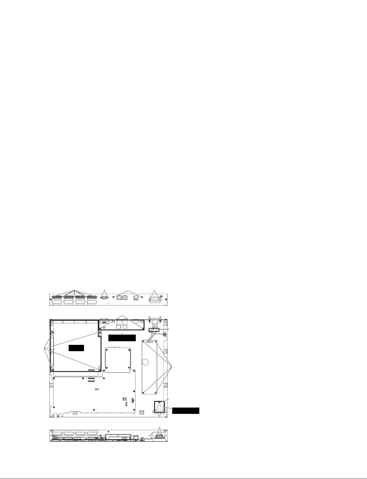
5. DAC1 Circuit Board (Time required: 6 minutes)
5-1 Remove the top cover. (See Procedure 1.)
5-2 Remove the DAC2 circuit board. (See Procedure 4.)
5-3 Remove the four (4) screws marked [400a] fixing
the circuit board and eight (8) screws marked [460]
from the rear panel. The D A C1 circuit board can then
be removed. (Fig. 3)
6. DAC-JACK Circuit Board (Time required: 2 minutes)
6-1 Remove the top cover. (See Procedure 1.)
6-2 Remove the two (2) screws marked [400b] from the
circuit board, two (2) jack sockets marked [190] and
two (2) screws marked [410] from the rear panel.
The DA C-J ACK circuit board can then be removed.
(Fig. 3)
7. Power Unit (Time required: 2 minutes)
7-1 Remove the top cover. (See Procedure 1.)
7-2 Remove the four (4) screws marked [400c] from the
circuit board. The power unit can then be removed.
(Fig. 3)
8. AC INLET Assembly (Time required: 2 minutes)
8-1 Remove the top cover. (See Procedure 1.)
8-2 Remove the two (2) supports marked [40] from the
rear panel. The AC INLET assembly can then be
removed. (Fig. 3)
5. DAC1 シート(所要時間:6分)
5-1. トップカバーを外します。(1項参照)
5-2. DAC2シートを外します。(4 項参照)
5-3. シートを止めているネジ[400a]4本とリアパネルの
ネジ[460]8 本を外し、DAC1シートを外します。
(Fig. 3)
6. DAC-JACK シート(所要時間:2分)
6-1. トップカバーを外します。(1項参照)
6-2. シートのネジ[400b]2本、及びリアパネルのジャッ
クソケット[190]2 本とネジ[410]2本を外し、DACJACK シートを外します。(Fig.3)
7. 電源ユニット(所要時間:2 分)
7-1. トップカバーを外します。(1項参照)
7-2. シートのネジ[400c]4本を外し、電源ユニットを外
します。(Fig.3)
8. ACINLETAss'y(所要時間:2 分)
8-1. トップカバーを外します。(1項参照)
8-2. リアパネルのサポート[40]2本を外し、ACINLET
Ass'y を外します。(Fig.3)
[400a]
[460] [190]
DAC1
[410]
[400b]
DAC-JACK
[40]
POWER
Supply Unit
(電源
ユニット)
[490]
Ferrite Core
(フェライト)
[400c]
[400d]
DAC-PSW
[400]: Bind Head Tapping Screw-B 3.0X6 MFZN2BL (EP600230)
[410]: Bonding Screw 3.0X8 MFZN2BL (VP157800)
[490]: Bind Head Tapping Screw-S 3.0X6 MFZN2BL (EP630210)
Fig.3
+バインドBタイト
+ボンディング小ネジ
+バインドSタイト
11
ACU16-C
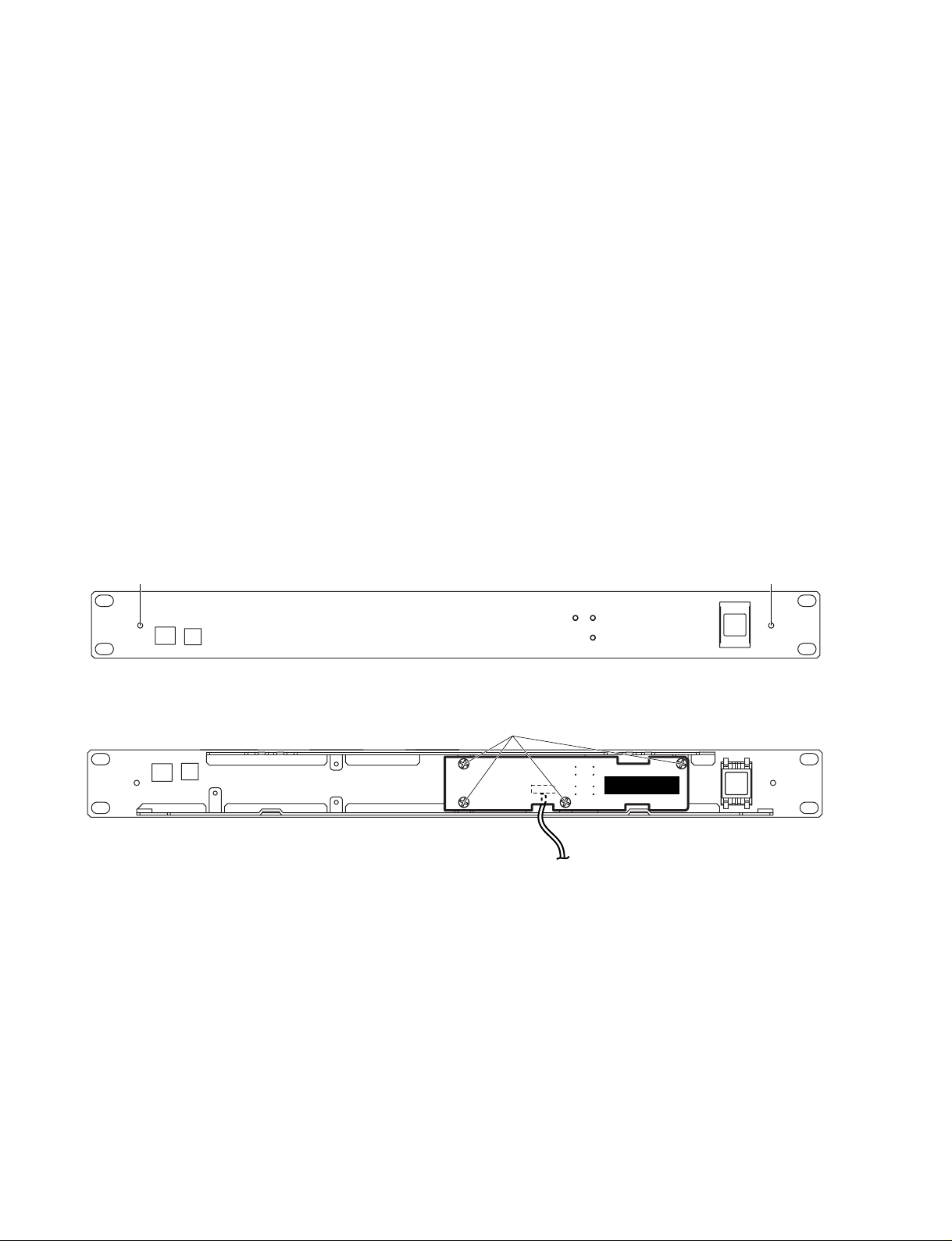
9. DAC-LED Circuit Boar d (Time required: 2 minutes)
9-1 Remove the top cover. (See Procedure 1.)
9-2 Remove the two (2) screws marked [480] from the
front panel and then remove the front panel
assembly.
9-3 Remove the four (4) screws marked [400] from the
circuit board. The DAC-LED circuit board can then
be removed. (Fig. 4)
10. DA C-PSW Circuit Board (Time required: 2 minutes)
10-1 Remove the top cover. (See Procedure 1.)
10-2 Remove the front panel assembly. (See Procedure 9-2.)
10-3 Remove the PSW knob.
10-4 Remove the two (2) screws marked [490] fixing the
switch and one (1) screw marked [400d] fixing the
circuit board. The DAC-PSW circuit board can then
be removed. (Fig. 3)
[480]
9. DAC-LED シート(所要時間:2分)
9-1. トップカバーを外します。(1 項参照)
9-2. フロントパネルのネジ[480]2本を外し、フロントパ
ネル Ass'yを外します。
9-3. シートのネジ[400]4本を外し、DAC-LEDシートを
外します。(Fig.4)
10. DAC-PSW シート(所要時間:2 分)
10-1. トップカバーを外します。(1 項参照)
10-2. フロントパネル Ass'y を外します。(9-2 項参照)
10-3. PSW ノブを外します。
10-4. スイッチを止めているのネジ[490]2本とシートを止
めているネジ[400d]1本を外し、DAC-PSWシート
を外します。(Fig.3)
[480]
[400]
[400]: Bind Head Tapping Screw-B 3.0X6 MFZN2BL (EP600230)
[480]: Bind Tapping Screw-S 3.0X6 MFZN2BL (V7451800)
+バインドBタイト
ボンディングSタイト
Fig.4
DAC-LED
12
ACU16-C
PIN
NO.
I/O FUNCTIONNAME
PIN
NO.
I/O FUNCTIONNAME
1
2
3
4
5
6
7
8
9
10
11
12
13
14
15
16
17
18
19
20
21
22
23
24
25
26
27
28
29
30
31
32
33
34
35
36
37
38
39
40
41
42
43
44
45
46
47
48
49
50
51
52
53
54
55
56
DACK0
PE15
VSS
A0
A1
A2
A3
A4
A5
A6
A7
A8
A9
A10
A11
A12
A13
A14
A15
A16
VCC
A17
VSS
/RAS
/CASL
/CASH
VSS
RDWR / PB5
A18
A19
A20
/IRQ7/A21
VSS
/RD
/WDTOVF
/WRH
VCC
/WRL
VSS
/CS1
/CS0
/IRQ3 / TCLKC
/IRQ2 / TCLKC
/CS3
/CS2
/IRQ1
TXD1
RXD1
SCKO
PA1 / TXD0
PA0 / RXD0
D15
D14
D13
VSS
D12
O
O
I
O
O
O
O
O
O
O
O
O
O
O
O
O
O
O
O
O
I
O
I
O
O
O
O
O
O
O
O
O
I
O
O
O
I
O
I
O
O
O
I
O
O
I
O
I
I
O
I
I/O
I/O
I/O
I
I/O
(Port E)
Port E
Ground
Address bus
Power supply
Address bus
Ground
Row address strobe
Column address strobe (low)
Column address strobe (high)
Ground
DRAM read/write / Port B
Address bus
Port B / Address bus
Ground
Read
Watch dog timer overflow
High write
Power supply
Low write
Ground
Chip select
Chip select
Port A / Timer clock
Interrupt request / Timer clock
Chip select
Chip select
Interrupt request
Data transmission
Data reception
Interrupt request
Port A / Data transmission
Port A / Data reception
Data bus
Ground
Data bus
57
58
59
60
61
62
63
64
65
66
67
68
69
70
71
72
73
74
75
76
77
78
79
80
81
82
83
84
85
86
87
88
89
90
91
92
93
94
95
96
97
98
99
100
101
102
103
104
105
106
107
108
109
110
111
112
D11
D10
D9
D8
VSS
D7
D6
D5
VCC
D4
D3
D2
D1
D0
VSS
XTAL
MD3
EXTAL
MD2
NMI
VCC
MD1
MD0
PLLVCC
PLLCAP
PLLVSS
PA15 / CK
/RES
/DREQ0
PE1
PE2
PE3
PE4
VSS
AN0 / PF0
AN1 / PF1
AN2 / PF2
AN3 / PF3
AN4 / PF4
AN5 / PF5
AVSS
AN6 / PF6
AN7 / PF7
AVCC
VSS
TIOC1B
VCC
PE6
PE7
PE8
PE9
PE10
VSS
PE11
PE12
PE13
I/O
I/O
I/O
I/O
I
I/O
I/O
I/O
I
I/O
I/O
I/O
I/O
I/O
I
I
I
I
I
I
I
I
I
I
I
I
O
I
I
I
I
I
I
I
I
I
I
I
I
I
I
I
I
I
I
O
I
O
O
O
O
O
I
O
O
O
Data bus
Ground
Data bus
Power supply
Data bus
Ground
Crystal oscillator
Mode control
Crystal oscillator
Mode control
Non-maskable interrupt request
Power supply
Mode control
Mode control
PLL Power supply
PLL capacitor
PLL Ground
Port A / Clock
Reset
Port E
Ground
Analog input / Port F
Analog ground
Analog input / Port F
Analog input / Port F
Power supply
Ground
(Port E)
Power supply
Port E
Ground
Port E
HD6477042AF28 (X3250A00A00) CPU
MAIN: IC201
LSI PIN DESCRIPTION
(LSI端子機能表)
13
ACU16-C
YSS904-F (XV989A00) DSP5 (Digital Signal Processor)
PIN
NO.
100
101
102
103
104
/RD
Vss
Vss
Vss
Vss
Vss
Vss
NC
NC
NC
NC
Vss
XO
CKI
Vss
/IC
NC
NC
NC
Vss
/CS
NC
NC
NC
NC
NC
NC
NC
NC
NC
NC
NC
NC
I/O
Not used
I
XI
O
O
I
O
I
O
I
I
I
I
I
I
I
I
I
I
I
I
I
I
I
I/O
I/O
I/O
I/O
I/O
I/O
I/O
I/O
I/O
I/O
I/O
I/O
I/O
I/O
I/O
I/O
O
I/O
I/O
I/O
I/O
I/O
I/O
I/O
I/O
I/O
I/O
I/O
I/O
I/O
I/O
I/O
I/O
I/O
I/O
I/O
I/O
I/O
I/O
I/O
I/O
I/O
I/O
I/O
I/O
Ground
Power supply
System master clock input (60 MHz or 30 MHz)
System master clock output (High or 30 MHz)
Ground
Sync. signal input
Sync. signal output
Ground
System clock input (30 MHz)
System clock output (30 MHz)
System master clock select
Power supply
Serial clock input (256 fs)
Serial. signal input
Initial clear
Test mode setting (0: TEST, 1: Normal)
Not used
Ground
Power supply
Chip select
Write enable input
Read enable input
CPU address bus
Power supply
Ground
CPU data bus
Power supply
Not used
Ground
CPU data bus
Wait output
Power supply
Serial data bus
Power supply
Ground
Serial data bus
Power supply
Ground
Serial data bus
Power supply
Ground
Serial data bus
Not used
FUNCTION
NAME
1
2
3
4
5
Vdd
6
7
8
9
Vdd
10
/SYNCI
11
/SYNCO
12
Vdd
13
14
CKO
15
CKSEL
16
17
MCKD
18
/SSYNC
19
20
/TEST
21
22
23
24
Vdd
25
26
27
/WR
28
29
CA7
30
CA6
31
CA5
32
CA4
33
CA3
34
CA2
35
CA1
36
37
Vdd
38
CD15
39
CD14
40
CD13
41
CD12
42
CD11
43
CD10
44
CD09
45
CD08
46
CD07
47
CD06
48
49
50
51
52
53
54
55
56
57
Vdd
58
Vdd
59
CD05
60
CD04
61
CD03
62
CD02
63
CD01
64
CD00
65
/WAIT
66
67
SIO00
68
SIO01
69
SIO02
70
SIO03
71
SIO04
72
SIO05
73
SIO06
74
SIO07
75
76
Vdd
77
SIO08
78
SIO09
79
SIO10
80
SIO11
81
SIO12
82
SIO13
83
SIO14
84
SIO15
85
86
Vdd
87
SIO16
88
SIO17
89
SIO18
90
SIO19
91
SIO20
92
SIO21
93
SIO22
94
SIO23
95
96
Vdd
97
SIO24
98
SIO25
99
SIO26
SIO27
PIN
NO.
105
106
107
108
109
110
111
112
113
114
115
116
117
118
119
120
121
122
123
124
125
126
127
128
129
130
131
132
133
134
135
136
137
138
139
140
141
142
143
144
145
146
147
148
149
150
151
152
153
154
155
156
157
158
159
160
161
162
163
164
165
166
167
168
169
170
171
172
173
174
175
176
177
178
179
180
181
182
183
184
185
186
187
188
189
190
191
192
193
194
195
196
197
198
199
200
201
202
203
204
205
206
207
208
NAME
NC
NC
NC
NC
SIO28
SIO29
SIO30
SIO31
Vss
Vdd
SIO32
SIO33
SIO34
SIO35
SIO36
SIO37
SIO38
SIO39
Vss
Vdd
SIO40
SIO41
SIO42
SIO43
SIO44
SIO45
SIO46
SIO47
Vss
SIO48
SIO49
SIO50
SIO51
SIO52
SIO53
SIO54
SIO55
Vss
Vdd
Vdd
SIO56
SIO57
SIO58
SIO59
SIO60
SIO61
SIO62
SIO63
NC
NC
NC
NC
NC
NC
NC
NC
Vss
/POE
Vss
PIO00
PIO01
PIO02
PIO03
PIO04
PIO05
PIO06
PIO07
Vss
Vdd
Vdd
PIO08
PIO09
PIO10
PIO11
PIO12
PIO13
PIO14
PIO15
Vss
NC
PIO16
PIO17
PIO18
PIO19
PIO20
PIO21
PIO22
PIO23
Vss
Vdd
Vdd
PIO24
PIO25
PIO26
PIO27
PIO28
PIO29
PIO30
PIO31
Vss
NC
NC
NC
NC
MAIN: IC601
I/O
Not used
I/O
I/O
I/O
I/O
I/O
I/O
I/O
I/O
I/O
I/O
I/O
I/O
I/O
I/O
I/O
I/O
I/O
I/O
I/O
I/O
I/O
I/O
I/O
I/O
I/O
I/O
I/O
I/O
I/O
I/O
I/O
I/O
I/O
I/O
I/O
I/O
I
I/O
I/O
I/O
I/O
I/O
I/O
I/O
I/O
I/O
I/O
I/O
I/O
I/O
I/O
I/O
I/O
I/O
I/O
I/O
I/O
I/O
I/O
I/O
I/O
I/O
I/O
I/O
I/O
I/O
I/O
I/O
I/O
Serial data bus
Power supply
Ground
Serial data bus
Power supply
Ground
Serial data bus
Power supply
Serial data bus
Power supply
Ground
Serial data bus
Not used
Power supply
Parallel data bus controll signal
Power supply
Parallel data bus
Power supply
Ground
Parallel data bus
Power supply
Not used
Parallel data bus
Power supply
Ground
Parallel data bus
Power supply
Not used
FUNCTION
14
ACU16-C
PIN
No.
NAME I/O FUNCTION
PIN
No.
NAME I/O FUNCTION
1
2
3
4
5
6
7
8
9
10
11
12
13
14
DVSS
DVDD
MCLK
PD
BICK
SDATA
LRCK
SMUTE
CS
DFS
DEM0
CCLK
DEM1
CDTI
DIF0
DIF1
DIF2
-
I
I
I
I
I
I
I
I
I
I
I
I
I
I
I
Digital Ground Pin
Digital Power Supply Pin, 3.3V or 5.0V
Master Clock Input Pin
Power-Down Mode Pin
When at "L",the Ak4393 is in power-down
mode and is held in reset.
The AK4393 should always be reset
upon power-up.
Audio Serial Data Clock Pin
The clock of 64fs or more than is
recommended to be input on this pin.
Audio Serial Data Input Pin
2's complement MSB-first data is input on this pin.
L/R Clock Pin
Soft Mute Pin
When this pin goes "H", soft mute cycle is initiated.
When returning "L",the output mute releases.
Chip Select Pin in serial mode
Doubla speed sampling mode Pin
(Internal pull-down pin)
"L":Normal Speed, "H":Double Speed
De-emphasis Enable pin
Control Data Clock Pin in serial mode
De-emphasis Enable pin
Control Data Input Pin in serial mode
Digital Input Format Pin
15
16
17
18
19
20
21
22
23
24
25
26
27
28
BVSS
VREFL
VREFH
AVDD
AVSS
AOUTR-
AOUTR+
AOUTL-
AOUTL+
VCOM
P/S
CKS0
CKS1
CKS2
I
I
-
-
O
O
O
O
O
O
I
I
I
I
Substrate Ground Pin, 0V
Low Level Voltage Reference Input Pin
High Level Voltage Reference Input Pin
Analog Power Supply Pin,5V
Analog Ground Pin, 0V
Rch Negative analog output Pin
Rch Positive analog output Pin
Lch Negative analog output Pin
Lch Positive analog output Pin
Common Voltage Output Pin,2.6V
Parallel/Serial Select Pin(Internal pull-up pin)
"L":Serial control mode,"H": Parallel control mode
Master Clock Select Pin
AK4393-VF-E2 (XW029A00) DAC
DAC: IC203, 204, 303, 304, 403, 404, 503, 504
YM3436DK (XG948E0) DIR2 (Digital Format Interface Receiver)
PIN
NO.
DAUX
1
HDLT
2
DOUT
3
VFL
4
OPT
5
SYNC
6
MCC
7
8
MCB
9
MCA
10
SKSY
11
12
13
P256
14
LOCK
15
16
17
DIM1
18
DIM0
19
DOM1
20
DOM0
21
KM1
22
WC
XI
XO
Vss
TC
I/O FUNCTIONNAME
I
O
O
O
O
O
O
O
O
O
I
I
O
O
O
O
I
I
I
I
I
Auxiliary input for audio data
Asynchronous buffer operation flag
Audio data output
Parity flag output
Fs x 1 Synchronous output signal for DAC
Fs x 1 Synchronous output signal for DSP
Fs x 64 Bit clock output
Fs x 1 Word clock output
Fs x 128 Bit clock output
Fs x 256 Bit clock output
Clock synchronization control input
Crystal oscillator connection or external
clock input
Crystal oscillator connection
VCO oscillating clock connection
PLL lock flag
Logic section power (GND)
PLL time constant switching output
Data input mode selection
Data input mode selection
Data output mode selection
Data output mode selection
Clock mode switching input 1
PIN
NO.
23
RSTN
24
Vdda
25
CTLN
26
PCO
27
(NC)
28
CTLP
29
Vssa
30
TSTN
31
KM2
32
KM0
33
FS1
34
FS0
35
CSM
36
EXTW
37
DDIN
38
39
Vdd
40
ERR
41
EMP
42
CD0
43
CCK
44
CLD
LR
I/O FUNCTIONNAME
I
System reset input
VCO section power (+5V)
I
VCO control input N
O
PLL phase comparison output
I
VCO control input P
VCO section power (GND)
I
Test terminal. Open for normal use
I
Clock mode switching input 2
I
Clock mode switching input 0
O
Channel status sampling frequency
display output 1
O
Channel status sampling frequency
display output 0
I
Channel status output method selection
I
External synchronous auxiliary input
word clock
I
EIAJ (AES/EBU) data input
O
PLL word clock output
Logic section power (+5 V)
O
Data error flag output
O
Channel status emphasis control code
output
O
3-wire type microcomputer interface data
output
I
3-wire type microcomputer interface clock
input
I
3-wire type microcomputer interface load
input
MAIN: IC502
15
ACU16-C
MBCG46183-129PFV-G
PIN
NO.
10
11
12
13
14
15
16
17
18
19
20
21
22
23
24
M37641M8-140FP
PIN
NO.
1
2
3
4
5
6
7
8
9
10
11
12
13
14
15
16
17
18
19
20
21
22
23
24
25
26
27
28
29
30
31
32
33
34
35
36
37
38
39
40
NAME I/O FUNCTION
1
2
3
4
5
6
7
8
9
D5 I/O
D6 I/O Data bus
D7 I/O
/IRQ0 I/O Interrupt request
/IRQ1 I/O Interrupt request
VSS6 Ground
/IRQ2 I/O Interrupt request
/IRQ3 I/O Interrupt request
/RD I Read
/WR I Write
/CE I Chip enable
/ASTB I
TESTI0 I Test mode
RX0 I
TX 0 O
RX1 I
TX 1 O
VSS18 Ground
VDD19 Power supply
RX2 I
TX2 O
RX30 I
TX 30 O
RX31 I
(X2485100) CPU
I/O FUNCTIONNAME
DQ1
DQ0
~IBF0
OBF0
CNVSS/VPP
~RESET
VSS
XOUT
VCC
AVCC
AVSS
PB7
PB6
PB5
PB4
PB3
PB2
PB1
PB0
~W
~R
A0
S0
P51
P50
XIN
LPF
P44
P43
P42
P41
P40
P37
P36
P35
P34
P33
P32
P31
P30
I/O
8 bit INPUT/OUTPUT PORT
I/O
8 bit INPUT/OUTPUT PORT
I/O
8 bit INPUT/OUTPUT PORT
I/O
8 bit INPUT/OUTPUT PORT
I/O
8 bit INPUT/OUTPUT PORT
I/O
8 bit INPUT/OUTPUT PORT
I/O
8 bit INPUT/OUTPUT PORT
I/O
8 bit INPUT/OUTPUT PORT
I
POWER SUPPLY
I
RESET INPUT
I/O
8 bit INPUT/OUTPUT PORT
I/O
8 bit INPUT/OUTPUT PORT
POWER SUPPLY
I
CLOCL INPUT
O
CLOCK OUTPUT
POWER SUPPLY
ANALOG POWER SUPPLY
O
ROOP FILTER
I/O
8 bit INPUT/OUTPUT PORT
I/O
8 bit INPUT/OUTPUT PORT
I/O
8 bit INPUT/OUTPUT PORT
I/O
8 bit INPUT/OUTPUT PORT
I/O
8 bit INPUT/OUTPUT PORT
I/O
8 bit INPUT/OUTPUT PORT
I/O
8 bit INPUT/OUTPUT PORT
I/O
8 bit INPUT/OUTPUT PORT
I/O
8 bit INPUT/OUTPUT PORT
I/O
8 bit INPUT/OUTPUT PORT
I/O
8 bit INPUT/OUTPUT PORT
I/O
8 bit INPUT/OUTPUT PORT
I/O
8 bit INPUT/OUTPUT PORT
I/O
8 bit INPUT/OUTPUT PORT
I/O
8 bit INPUT/OUTPUT PORT
I/O
8 bit INPUT/OUTPUT PORT
I/O
8 bit INPUT/OUTPUT PORT
I/O
8 bit INPUT/OUTPUT PORT
I/O
8 bit INPUT/OUTPUT PORT
I/O
8 bit INPUT/OUTPUT PORT
I/O
8 bit INPUT/OUTPUT PORT
I/O
8 bit INPUT/OUTPUT PORT
(XV833A00) CPU
Serial data
Serial data
PIN
NO.
PIN
NO.
41
42
43
44
45
46
47
48
49
50
51
52
53
54
55
56
57
58
59
60
61
62
63
64
65
66
67
68
69
70
71
72
73
74
75
76
77
78
79
80
NAME I/O FUNCTION
TX3
25
26
27
28
29
30
31
32
33
34
35
36
37
38
39
40
41
42
43
44
45
46
47
48
USB_D+
USB_D-
EXT.CAP
1O
RX32 I
TX32 O
Serial data
RX33 I
TX33 I/O
/IC I Initial Clear
VSS31 Ground
XI I Crystal quarts input
VSS33 Ground
XO O Cry stal quarts output
A0 I
A1 I
A2 I
A3 I
Address bus
A4 I
A5 I
CPUCLK I Clock
VSS42 Ground
VDD43 Power supply
D0 I/ O
D1 I/ O
D2 I/ O
Data bus
D3 I/ O
D4 I/ O
I/O FUNCTIONNAME
P17
I/O
P16
P15
P14
P13
P12
P11
P10
PO7
PO6
PO5
PO4
PO3
PO2
PO1
PO0
P27
P26
P25
P24
P23
P22
P21
P20
P74
P73
P72
P71
P70
VSS
VCC
DQ7
DQ6
DQ5
DQ4
DQ3
DQ2
8 bit INPUT/OUTPUT PORT
I/O
8 bit INPUT/OUTPUT PORT
I/O
8 bit INPUT/OUTPUT PORT
I/O
8 bit INPUT/OUTPUT PORT
I/O
8 bit INPUT/OUTPUT PORT
I/O
8 bit INPUT/OUTPUT PORT
I/O
8 bit INPUT/OUTPUT PORT
I/O
8 bit INPUT/OUTPUT PORT
I/O
8 bit INPUT/OUTPUT PORT
I/O
8 bit INPUT/OUTPUT PORT
I/O
8 bit INPUT/OUTPUT PORT
I/O
8 bit INPUT/OUTPUT PORT
I/O
8 bit INPUT/OUTPUT PORT
I/O
8 bit INPUT/OUTPUT PORT
I/O
8 bit INPUT/OUTPUT PORT
I/O
8 bit INPUT/OUTPUT PORT
I/O
8 bit INPUT/OUTPUT PORT
I/O
8 bit INPUT/OUTPUT PORT
I/O
8 bit INPUT/OUTPUT PORT
I/O
8 bit INPUT/OUTPUT PORT
I/O
8 bit INPUT/OUTPUT PORT
I/O
8 bit INPUT/OUTPUT PORT
I/O
8 bit INPUT/OUTPUT PORT
I/O
8 bit INPUT/OUTPUT PORT
I/O
5 bit INPUT/OUTPUT PORT
I/O
5 bit INPUT/OUTPUT PORT
I/O
5 bit INPUT/OUTPUT PORT
I/O
5 bit INPUT/OUTPUT PORT
I/O
5 bit INPUT/OUTPUT PORT
I/O
USB D+ VOLTAGE
I/O
USB D- VOLTAGE
I/O
LINE POWER SUPPLY
POWER SUPPLY
POWER SUPPLY
I/O
8 bit INPUT/OUTPUT PORT
I/O
8 bit INPUT/OUTPUT PORT
I/O
8 bit INPUT/OUTPUT PORT
I/O
8 bit INPUT/OUTPUT PORT
I/O
8 bit INPUT/OUTPUT PORT
I/O
8 bit INPUT/OUTPUT PORT
MAIN: IC301
MAIN: IC316
16
ACU16-C
IC BLOCK DIAGRAM
TC74LVX4245FS (XU229A00)
MAIN: IC403
TRANSCEIVER
V
CCA VCCB
1
2DIR
22G
3A1
10A8
TC74VHC138FT
Same as above block
(XZ495A00)
MAIN: IC205, IC206
3-8 DEMULTIPLEXER
Converter
Logic
Level
23
131211
(IC ブロック図)
1
VCCA
2
DIR
3
GND
GND
A1
A2
4
5
A3
6
A4
7
A5
8
A6
9
A7
10
A8
11
12
24
21
B1
14
B8
TC74VHC163FT (X2378A00)
MAIN: IC313, 507, 508
(TOP VIEW)
24
CCB
V
23
VCCB
22
G
21
B1
20
B2
19
B3
18
B4
17
B5
16
B6
15
B7
14
B8
INPUTS
OUTPUTS
DIR A-BUS B-BUS
GND
G
L
L
H
L
H
X
13
FUNCTION
A=B OUTPUT INPUT
B=A INPUT OUTPUT
Z High lmpedance
TC74VHC244FT (XW234A00)
MAIN: IC402, IC408, IC409
BUS BUFFER
X : Don't Care
Z : High lmpedance
1
A
Select
Enable
Output
GND
G2A
G2B
2
B
3
C
4
G2A
5
G2B
6
G1
G1
7
Y7 Y5
Y7
8
TC74VHC32FT
16
A
B
15
Y0
14
C
Y1
13
Y2
12
Y3
11
Y4
10
Y6
9
(XY945A00)
MAIN: IC210, IC213, IC216, IC217
OR
1
2
1B
31A1Y
42A
52B
62Y
7GND
14
13
12
11 4Y
10 3B
93A
83Y
1
1G
16
R
C
QA
CLEAR
QB
QC
QD
EN
T
15
14
13
12
11
10
9
Vcc
RIPPLE
CARRY
OUTPUT
QA
QB
QC
QD
ENABLE
T
LOAD
1A1
2Y4
1A2
2Y3
1A3
2Y2
1A4
2Y1
(GND) Vss
2
3
4
5
6
7
8
9
10
1
Vcc
YO
Y1
Y2
Output
Y3
Y4
Y5
Y6
CLEAR
CLOCK
ENABLE
P
GND
2
CK
3
A
A
4
B
B
C
5
C
LOAD
6
D
D
EN
7
P
8
20
DD (Vcc)
V
19
2G
18
1Y1
17
2A4
16
1Y2
15
2A3
14
1Y3
13
2A2
12
1Y4
11
2A1
TC7S04F (XM182A00)
DAC: IC211, IC411
TC7SH04FU (XS775A00)
MAIN: IC413, IC419
INVERTER
Vcc
4B
4A
VSS
1
NC
2
IN
3
5
VDD
4
OUT
17
ACU16-C
TC74VHC245FT(XU797A00)
DAC: IC201, IC202, IC401, IC402
MAIN: IC219, IC503, 602, 603
74VHC245MTCX (X0296A00)
MAIN: IC219, IC503
TC74VHCT245AFT(XT744A00)
MAIN: IC407, IC410
BUFFER
V
CC
20
G
19
B1
18
B2
17
B3
16
B4
15
B5
14
B6
13
B7
12
11
B8
GND
1D1R
A1
2
A2
3
A3
4
A4
5
A5
6
A6
7
A7
8
A8
9
10
DS36276M (X2155A00)
MAIN: IC307
RO
1
RE
2
3
DE
4
DI
8
V
R
D
CC
7
DO/RI
6
DO/RI
GND
5
TC74VHC74FT (XV892A00)
MAIN: IC212
D-FF
1
1CLR
2
D
1D
3
1CK
1PR
GND
PR CLR CLK D Q Q
L
H
L
H
H
H
CK
4
PR
5
Q
1Q
6
Q
1Q
7
INPUTS OUTPUTS
X
H
X
L
X
L
f
H
f
H
L
H
14
VCC
13
CLR
2CLR
D
12
CLR
2D
11
CK
2CK
10
2PRPR
9
Q
2Q
8
2QQ
H
X
X
X
H
L
X
L
L
H
H
H
H
L
L
H
O
O
Q
Q
HD74LV273ATELL (X2689A00)
MAIN: IC207, IC214, IC218, IC417
D-FF
V
CC
20
8Q
19
8D
18
7D
17
CK
DCK
CL
7Q
16
6Q
15
CK
D
6D
14
5D
13
CK
CL
Q
5Q
12
11
CLOCK
GND
1CLEAR
1Q
2
1D
3
2D
4
2Q
5
3Q
6
3D
7
4D
8
4Q
9
10
QQ
CL CL
CK CK
DD
D
CL
QQ
QQ
CL CL
CK
D
DDCK
CL
Q
NJM4580ED (XT157A00)
DAC: IC207-210, IC308-311, IC407-410,
IC508-511
µPC4570G2 (XF291A00)
DAC: IC205, IC206, IC306, IC307, IC405,
IC406, IC506, IC507
OP AMP
+DC Voltage
+-
+-
8
7
6
5
Supply
Output B
Inverting
Input B
Non-Inverting
Input B
Output A +V
Inverting
Input A
Non-Inverting
Input A
-DC Voltage Supply
1
2
3
4-V
SN75C1168NSR (XU073A00)
MAIN: IC302
LINE DRIVER
1
1B
2
1A
3
1R
4
1DE
5
2R
6
2A
7
2B
8
GND
18
TC74VHC04FT (X0195A00)
MAIN: IC509
INVERTER
16
Vcc
15
1D
14
1Y
13
1Z
12
2DE
11
2Z
10
2Y
9
2D
Vss
1
1A
2
1Y
3
2A
4
2Y
5
3A
6
3Y
7
14
VDD
13
6A
12
6Y
11
5A
10
5Y
9
4A
8
4Y
TC74VHC125FT (XY074A00)
MAIN: IC412, IC505, IC506
BUFFER
1
GND
C1
2
A1
3
Y1
4
C2
5
A2
6
Y2
7
14
Vcc
13
C4
12
A4
11
Y4
10
C3
9
A3
8
Y3
ACU16-C
TC7WH04FU
MAIN: IC419
INVERTER
1
2
3Y
2A
3
GND
4
W194-70G
MAIN: IC504
Clock Generator
4
FS0
FS1
5
(XW492A00)
FBIN
1
N
(XY363A00)
81A
Vcc
7
1Y
6
3A
5
2Y
TC7WH08FU (XW948A00)
MAIN: IC209
AND
CC
1
1A
2
1B
2Y
3
4
GND
7
VDD
3
GND
FBIN
IN
GND
FS0
V
8
1Y
7
6
2B
5
2A
1
2
3
4
TC7WH14FU
MAIN: 207, 317
SCHMITT INVERTER
3Y
2A
GND
OUT2
8
VDD
7
6
OUT1
5
FS1
(XY806A00)
1
2
3
4
81A
Vcc
7
1Y
6
3A
5
2Y
IN
(Reference
Input)
PHASE
2
DETECTOR
VCO
2
CHARGE
PUMP
LOOP
FILTER
OUTPU T
BUFFER
OUTPU T
BUFFER
6
OUT1
8
OUT2
19
ACU16-C
CIRCUIT BOARDS
MAIN Circuit Board
(シート基板図)
A
CN301: to DAC-JACK-CN601
CN604: to DAC2-CN401
CN603: to DAC1-CN201
20
A'
IN: 3NA-V848170
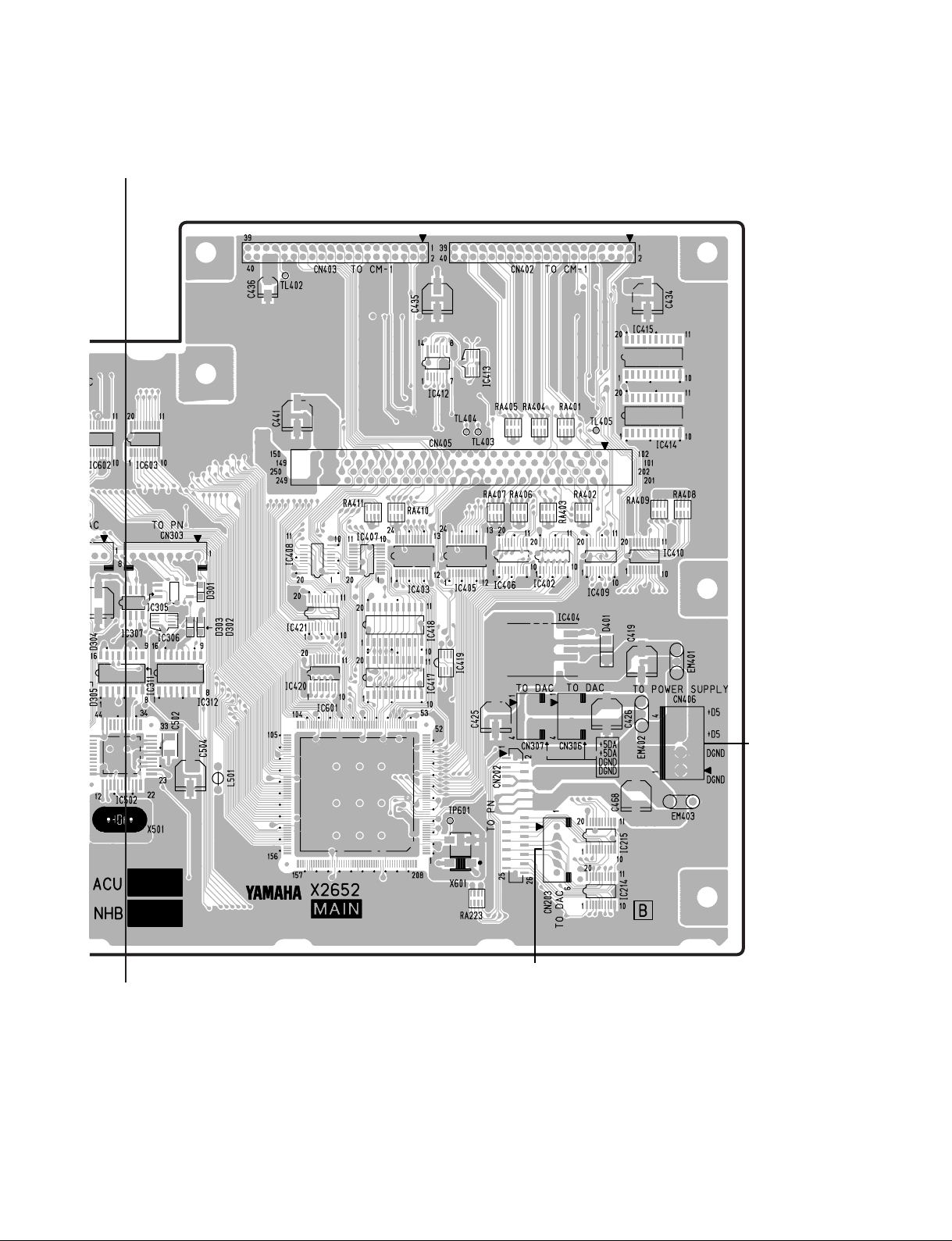
601
ACU16-C
A
CN403: to CM-1 CN402: to CM-1
A'
CN306: to DAC2-CN501
CN307: to DAC1-CN301
to POWER Supply
CN203: to DAC-LED-CN801
Component side(部品側)
21
 Loading...