

Yaesu FTM-350R, FTM-350AE, FTM-350E, FTM-350AR Technical Supplement
VERTEX STANDARD CO., LTD.
4-8-8 Nakameguro, Meguro-Ku, Tokyo 153-8644, Japan
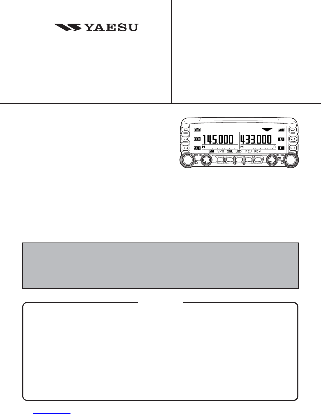
DUAL BAND FM TRANSCEIVER
FTM-350R/E
FTM-350AR/E
Technical Supplement
©2011 VERTEX STANDARD CO., LTD.
EH033M90D
VERTEX STANDARD
US Headquarters
10900 Walker Street, Cypress, CA 90630, U.S.A.
YAESU UK LTD.
Unit 12, Sun Valley Business Park, Winnall Close
Winchester, Hampshire, SO23 0LB, U.K.
VERTEX STANDARD HK LTD.
Unit 1306-1308, 13F., Millennium City 2, 378 Kwun Tong Road,
Kwun Tong, Kowloon, Hong Kong
VERTEX STANDARD (AUSTRALIA) PTY., LTD.
Tally Ho Business Park, 10 Wesley Court, East Burwood, VIC, 3151
Introduction
This manual provides technical information necessary for servicing the FTM-350AR/E Dual Band FM Transceiver.
Servicing this equipment requires expertise in handling surface-mount chip components. Attempts by non-qualified persons to service this equipment may result in permanent damage not covered by the warranty, and may be illegal in some
countries.
Two PCB layout diagrams are provided for each double-sided circuit board in the Transceiver. Each side of is
referred to by the type of the majority of components installed on that side (“leaded” or “chip-only”). In most
cases one side has only chip components, and the other has either a mixture of both chip and leaded components (trimmers, coils, electrolytic capacitors, ICs, etc.), or leaded components only.
While we believe the technical information in this manual to be correct, VERTEX STANDARD assumes no
liability for damage that may occur as a result of typographical or other errors that may be present. Your
cooperation in pointing out any inconsistencies in the technical information would be appreciated.
Important Note
The transceiver was assembled using Pb (lead) free solder, based on the RoHS specification.
Only lead-free solder (Alloy Composition: Sn-3.0Ag-0.5Cu) should be used for repairs performed on this apparatus. The solder stated above utilizes the alloy composition required for compliance with the lead-free specification,
and any solder with the above alloy composition may be used.
Contents
Specifications ......................................................2
Exploded View & Miscellaneous Parts............5
Block Diagram....................................................7
Alignment............................................................9
Board Unit
MAIN Unit Circuit Diagram (Lot.1~) ................... 17
MAIN Unit Parts Layout (Lot.1~).........................19
MAIN Unit Circuit Diagram (Lot.5~) ................... 21
MAIN Unit Parts Layout (Lot.5~).........................23
MAIN Unit Parts Layout (Lot.27~).......................25
MAIN Unit Parts List ............................................29
(Schematics, Layouts & Parts)
PANEL Unit Circuit Diagram (Lot.1~).................61
PANEL Unit Parts Layout (Lot.1~) ...................... 62
PANEL Unit Circuit Diagram (Lot.12~)...............63
PANEL Unit Parts Layout (Lot.12~) .................... 64
PANEL Unit Parts List .......................................... 65
PANEL-R Unit Circuit Diagram (Lot.1~).............71
PANEL-R Unit Parts Layout (Lot.1~) ..................72
PANEL-R Unit Circuit Diagram (Lot.6~).............73
PANEL-R Unit Parts Layout (Lot.6~) ..................74
PANEL-R Unit Circuit Diagram (Lot.12~)...........75
PANEL-R Unit Parts Layout (Lot.12~) ................76
PANEL-R Unit Parts List ...................................... 77
1FTM-350AR/E Technical Supplement

Specifications
General
Frequency Ranges: RX: 0.5-1.8 MHz (AM Radio)
76-108 MHz (FM Radio)
108-137 MHz (Air Band)
137-174 MHz (144 MHz HAM Band)
174-250 MHz (VHF TV Band)
300-420 MHz (General 1)
420-470 MHz (430 MHz HAM Band)
470-800 MHz (UHF TV Band)
800-1000 MHz (General 2: USA Cellular Blocked)
TX: 144-146(148) MHz (Ham Band)
222-225 MHz (USA only)
430-440(450) MHz (Ham Band)
Channel Steps: 5, 6.25, 8.33, (9), 10, 12.5, 15, 20, 25, 50, 100, 200 kHz
(9): AM Radio Only
Frequency Stability: ±5ppm (14 °F to +140 °F [–10 °C to +60 °C])
Repeater Shift: ±600 kHz (144 MHz)
±1.6 / 5.0 / 7.6 MHz (430 MHz)
Emission Type: F1, F2, F3,
Antenna Impedance: 50
Supply Voltage: Nominal: 13.8 V DC, Negative Ground
Operating: 11.7 ~ 15.8 V, Negative Ground
Current Consumption: 0.5 A (Receive)
10 A (TX, 144 MHz 50W)
10 A (TX, 430 MHz 50W)
Operating Temperature: –4 °F to +140 °F (–20 °C to +60 °C)
Case Size (WxHxD): Panel: 6.2” x 2.6” x 1.3” (157 x 66 x 33.5 mm) w/o knob & connectors
Rear Chassis: 5.5” x 1.8” x 5.9” (140 x 46 x150 mm) w/o connectors
Weight (Approx.) 4.6 lbs (2.1 kg) Panel + Rear Chassis + Connection Cable
Transmitter
RF Power Output: 50 / 20 / 5 W
Modulation Type: Variable Reactance F1, F2, F3
Maximum Deviation: ±5 kHz
Spurious Emission: At least 60 dB below
Microphone Impedance:2 k
2 FTM-350AR/E Technical Supplement

Receiver
Circuit Type: Double-Conversion Super heterodyne (FM/AM)
Triple-Conversion Super heterodyne (WFM)
Single-Conversion Super heterodyne (Radio)
Intermediate Frequencies: 1st: 47.25 MHz, 2nd: 450 kHz (“Main Side” Band, FM/AM)
1st: 44.85 MHz, 2nd: 450 kHz (“Sub Side” Band, FM/AM)
1st: 45.8 MHz, 2nd: 10.7MHz, 3rd: 1MHz (“Main Side” Band, WFM)
1st: 44.0 MHz, 2nd: 10.7MHz, 3rd: 400 kHz (“Sub Side” Band, WFM)
1st: 130 kHz (FM Radio)
1st: 50 kHz (AM Radio)
Sensitivity:5 μV TYP for 10 dB SN (0.5-1.7 MHz, AM)
2 μV TYP for 12 dB SINAD (76-108 MHz, WFM)
0.8 μV TYP for 10 dB SN (108-137 MHz, AM)
0.2 μV for 12 dB SINAD (137-140 MHz, FM)
0.2 μV for 12 dB SINAD (140-150 MHz, FM) EXP
0.25 μV for 12 dB SINAD (150-174 MHz, FM)
1 μV TYP for 12 dB SINAD (174-222 MHz, WFM)
0.8 μV TYP for 10 dB SN (300-336 MHz, AM)
0.25 μV TYP for 12 dB SINAD (336-420 MHz, FM)
0.2 μV for 12 dB SINAD (420-470 MHz, FM) EXP
5 μV TYP for 12 dB SINAD (470-540 MHz, WFM)
5 μV TYP for 12 dB SINAD (540-800 MHz, WFM)
0.4 μV TYP for 12 dB SINAD (800 -899.99 MHz, FM)
0.8 μV TYP for 12 dB SINAD (800 -999.99 MHz, FM)
USA Version Cellular Blocked
Squelch Sensitivity: 0.16 μV (144 / 430 MHz Band)
Selectivity (NFM, AM): 12 kHz / 30 kHz (–6 dB / –60 dB)
AF Output: 8 W @ 8 for 10 % THD (@ 13.8 V) BTL EXP SP
4 W @ 4 for 10 % THD (@ 13.8 V) Normal EXP SP
AF Output Impedance: 4-16
Specifications
Specifications are subject to change without notice, and are guaranteed within the 144/222/430 MHz amateur bands
only.
Cellular Blocked per FCC rule Part 15.121, may not receive 900 MHz Amateur band.
3FTM-350AR/E Technical Supplement
7
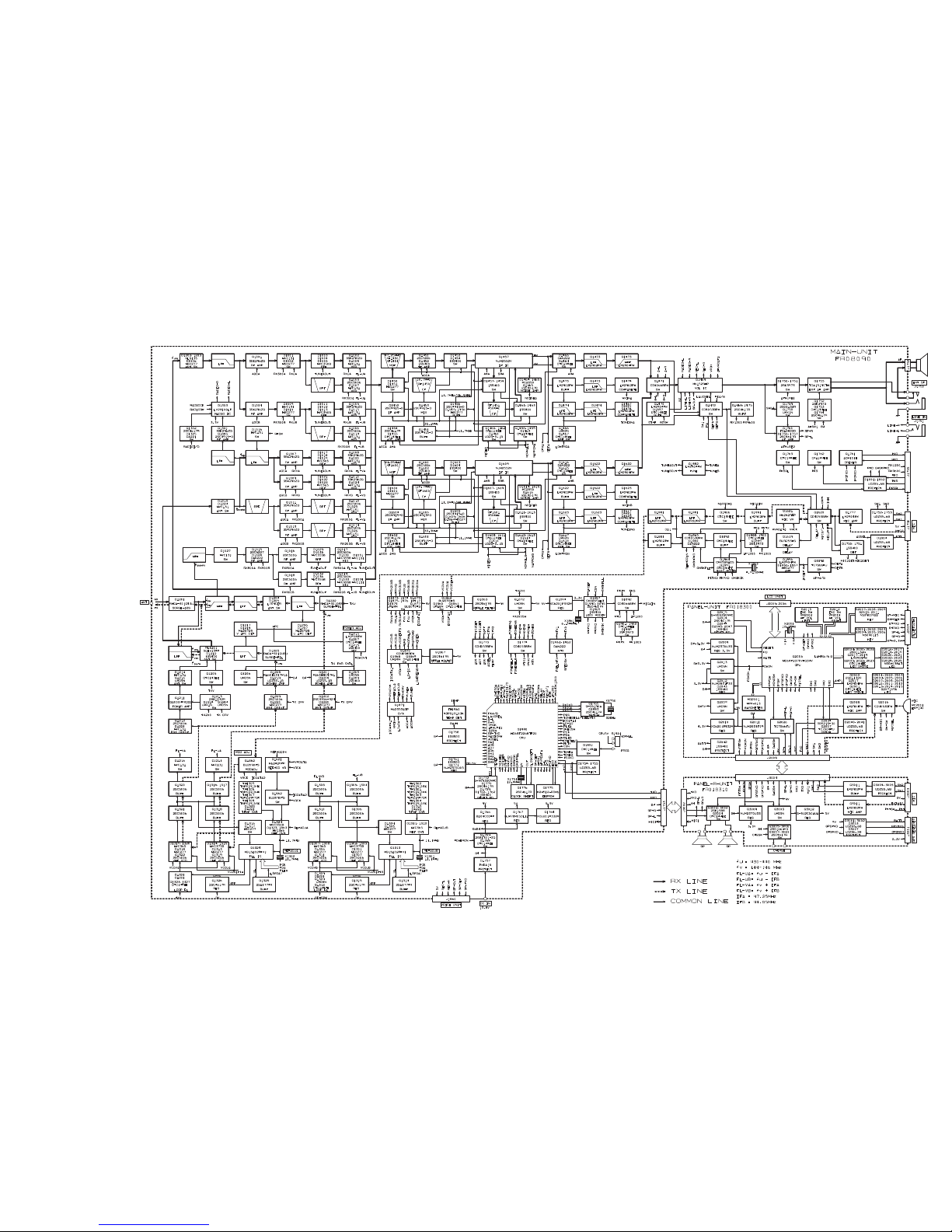
Block Diagram
FTM-350AR/E Technical Supplement

Alignment
Introduction
The FTM-350AR/E is carefully aligned at the factory
for the specified performance across the amateur
band. Realignment should therefore not be necessary except in the event of a component failure. Only
an authorized Vertex Standard representative should
perform all component replacement and service, or
the warranty policy may be void.
The following procedures cover the adjustments that
are not normally required once the transceiver has
left the factory. However, if damage occurs and some
parts subsequently are replaced, realignment may
be required. If a sudden problem occurs during normal operation, it is likely due to component failure;
realignment should not be done until after the faulty
component has been replaced.
We recommend that servicing be performed only by
authorized Vertex Standard service technicians who
are experienced with the circuitry and fully equipped
for repair and alignment. If a fault is suspected, contact the dealer from whom the transceiver was purchased for instructions regarding repair. Authorized
Vertex Standard service technicians realign all circuits and make complete performance checks to ensure compliance with factory specifications after replacing any faulty components.
Those who do undertake any of the following alignments are cautioned to proceed at their own risk.
Problems caused by unauthorized attempts at realignment are not covered by the warranty policy.
Also, Vertex Standard reserves the right to change
circuits and alignment procedures in the interest of
improved performance, without notifying owners.
Required Test Equipment
The following test equipment (and familiarity with
its use) is necessary for complete realignment. Correction of problems caused by misalignment resulting from use of improper test equipment is not covered under the warranty policy. While most steps
do not require all of the equipment listed, the interactions of some adjustments may require that more
complex adjustments be performed afterwards.
Do not attempt to perform only a single step unless
it is clearly isolated electrically from all other steps.
Have all test equipment ready before beginning and,
follow all of the steps in a section in the order presented.
RF Signal Generator with calibrated output level
at 1 GHz
Deviation Meter (linear detector)
In-line Wattmeter with 5% accuracy at 1 GHz
50-Ohm 100-W RF Dummy Load
4-Ohm AF Dummy Load
Regulated DC Power Supply adjustable from 11.5
to 16 VDC, 15A
Frequency Counter: 0.2-ppm accuracy at 1 GHz
AF Signal Generator
AC Voltmeter
DC Voltmeter: high impedance
SINAD Meter
Under no circumstances should any alignment be
attempted unless the normal function and operation
of the transceiver are clearly understood, the cause
of the malfunction has been clearly pinpointed and
any faulty components replaced, and realignment
determined to be absolutely necessary.
9FTM-350AR/E Technical Supplement
Alignment
Alignment Preparation & Precautions
A 50-Ohm RF load and in-line wattmeter must be
connected to the antenna jack in all procedures that
call for transmission; alignment is not possible with
an antenna. After completing one step, read the next
step to see if the same test equipment is required. If
not, remove the test equipment (except dummy load
and wattmeter, if connected) before proceeding.
Correct alignment requires that the ambient temperature be the same as that of the transceiver and
test equipment, and that this temperature be held
constant between 68 °F ~ 86 °F (20 °C ~ 30 °C). When
the transceiver is brought into the shop from hot or
cold air, it should be allowed some time to come to
room temperature before alignment. Whenever possible, alignments should be made with oscillator
shields and circuit boards firmly affixed in place.
Also, the test equipment must be thoroughly
warmed up before beginning.
Entering the Alignment Mode
Alignment of the FTM-350AR/E is performed using
a front panel software-based procedure. To perform
alignment of the transceiver, it must first be placed
in the “Alignment Mode,” in which the adjustments
will be made and then stored into memory.
To enter the Alignment mode:
1. Turn the radio on while pressing and holding the two
keys which are located on both sides of the [POWER]
switch.
2. Press the keys on the front panel in the following sequence.
[][][][][][]
Note: Signal levels in dB referred to in the alignment
procedure are based on 0dBμ = 0.5μV.
Test Setup
Set up the test equipment as shown below for transceiver alignment. Maintain the supply voltage at
13.8V DC for all steps.
50-ohm
Dummy Load
Freq. Counter
Deviation
Meter
AC Voltmeter
Inline
Wattmeter
Regulated
13.8V PSU
Sampling
Coupler
AF Generator
AC Voltmeter
[][]
3. The transceiver is now in the “Alignment Mode.”
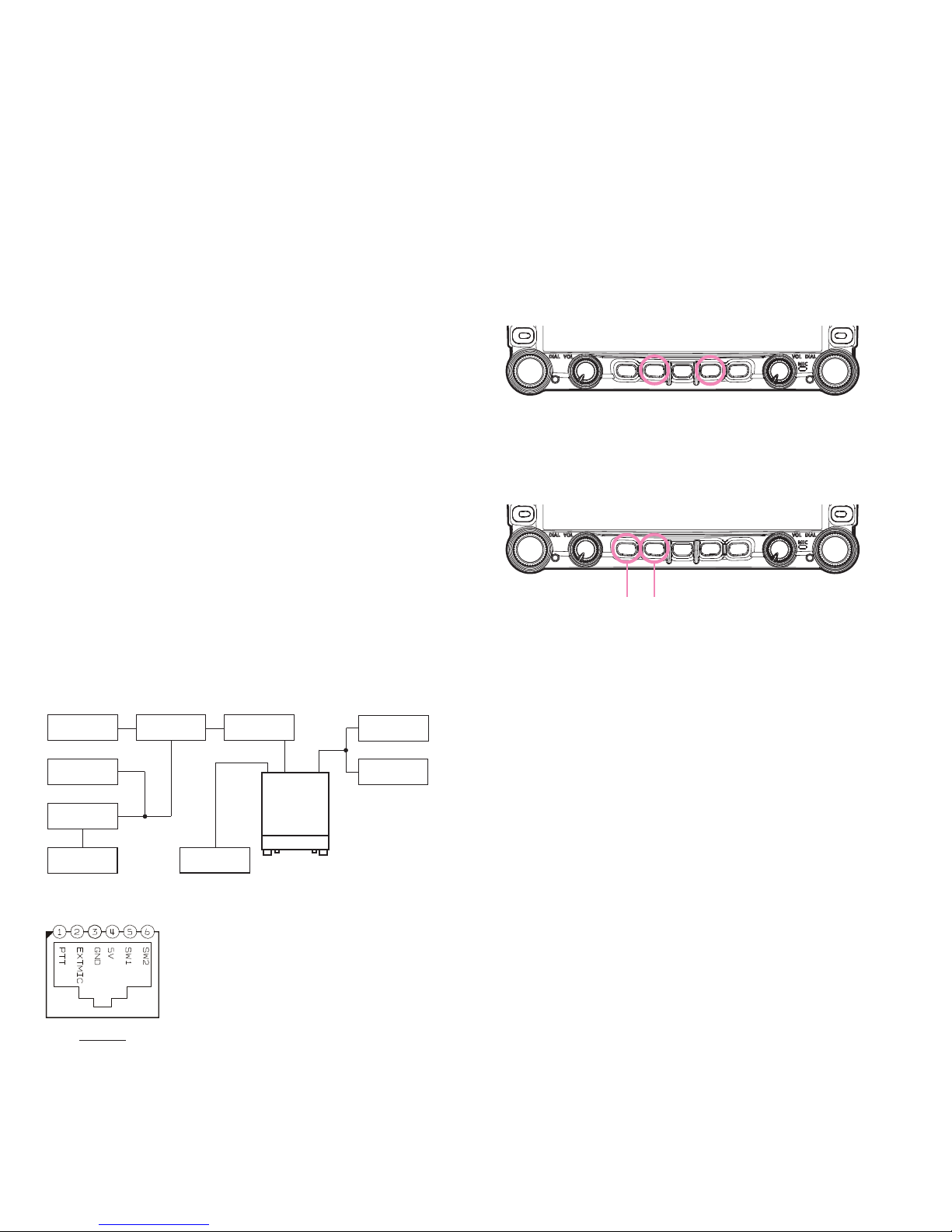
MIC Jack
10 FTM-350AR/E Technical Supplement

Alignment
VCO VCV Adjustment
Connect the DC voltmeter to TP1302 (MAIN) and
TP1301 (SUB). Referring to the table below, tune the
transceiver to each frequency listed. Confirm that the
correct voltage is present, or adjust the listed setting
for the required voltage.
MAIN
Tune to: TX/RX for
440.05 MHz RX 2.6 ± 0.25 V
440.00 MHz TX 1.9 ± 0.25 V
146.05 MHz RX 1.7 ± 0.25 V
146.00 MHz TX 1.5 ± 0.25 V
SUB
Tune to: TX/RX for
440.05 MHz RX 2.6 ± 0.30 V
395.05 MHz RX 1.9 ± 0.25 V
146.05 MHz RX 1.4 ± 0.25 V
190.05 MHz RX 1.4 ± 0.25 V
DC Voltmeter
1. Set the power supply voltage to 13.8 V.
[
2. Press the
Item to “
3. Press and hold in the
to save the new setting.
TX Power Adjustment
1. Press the
Item to “
2. Set the transceiver frequency to 440.000 MHz.
3. Press the
4. Press the PTT switch to activate the transmitter,
adjust the left DIAL knob so that the RF Power
Meter reading is 5 W (± 0.5 W).
5. Press the
6. Press the PTT switch to activate the transmitter,
adjust the left DIAL knob so that the RF Power
Meter reading is 20 W (± 0.5 W).
7. Press the
8. Press the PTT switch to activate the transmitter,
adjust the left DIAL knob so that the RF Power
Meter reading is 50 W (± 0.5 W).
9. Set the transceiver frequency to 146.000 MHz.
10.Press the
11.Press the PTT switch to activate the transmitter,
adjust the left DIAL knob so that the RF Power
Meter reading is 5 W (± 0.5 W).
12.Press the
13.Press the PTT switch to activate the transmitter,
adjust the left DIAL knob so that the RF Power
Meter reading is 20 W (± 0.5 W).
14.Press the
15.Press the PTT switch to activate the transmitter,
adjust the left DIAL knob so that the RF Power
Meter reading is 50 W (± 0.5 W).
BAT UPBAT UP
BAT UP”.
BAT UPBAT UP
[
FWD
[
BCK
[
ADJ
PWR xxxPWR xxx
PWR xxx”.
PWR xxxPWR xxx
ADJ
]
key
]
key
]
key
[
ADJ
[
POW
[
POW
[
POW
[
POW
[
POW
[
POW
]
key to set the alignment Menu
[
]
FWD
key for one second,
]
key to set the alignment Menu
]
key to select "LOW".
]
key to select "MID".
]
key to select "HIGH".
]
key to select "LOW".
]
key to select "MID".
]
key to select "HIGH".
TP1302 TP1301
The following steps is USA Version only.
16.Set the transceiver frequency to 223.550 MHz.
17.Press the PTT switch to activate the transmitter,
adjust the left DIAL knob so that the RF Power
Meter reading is 1 W (± 0.1 W).
11FTM-350AR/E Technical Supplement

Alignment
PLL Reference Frequency
1. Set the transceiver frequency to 440.000 MHz.
2. Press the
3. Press the
Item “
4. Press the PTT switch to activate the transmitter,
adjust the left DIAL knob, if necessary, so the
counter frequency is within 100 Hz of 440.000
MHz.
5. Press and hold in the
to set the alignment Menu Item “
6. Set the transceiver frequency to 440.050 MHz.
7. Press the
8. Rotate the left DIAL knob to select Menu Item "TX/
RX".
9. Press the left DIAL knob, then rotate the left DIAL
knob to select "B08 WIDE/NARROW AUTO".
10.Press the left DIAL knob, then rotate the left DIAL
knob to select "AUTO (FM)".
11.Press the
setting.
12.Connect the frequency counter fed through the
0.001μF capactor to the TP1303.
13.Adjust the left DIAL knob, as needed, so that the
counter frequency reading is 395.200 MHz (±100
Hz).
RF Front-end Tuning
1. Connect the DC voltmeter to TP1401 (MAIN) and
TP1601 (SUB) on the MAIN unit, then inject a
439.050 MHz signal at a level of +10 dBμV (with 1
kHz modulation ± 3.5 kHz deviation) from the
RF signal generator.
2. Set the transceiver frequency to 439.050 MHz.
3. Press the
Item “
4. Adjust the left DIAL knob for maximum deflec-
tion on the DC Voltmeter and then turn the dial
in the opposite direction until the meter deflection drops slightly lower than maximum.
5. Set the transceiver and RF signal generator frequency to 145.050 MHz.
6. Adjust the left DIAL knob for maximum deflec-
tion on the DC Voltmeter and then turn the dial
in the opposite direction until the meter deflection drops slightly low
7. Set the RF signal generator frequency to 439.050
MHz.
[
REFA xxxREFA xxx
REFA xxx”.
REFA xxxREFA xxx
[
TUNA xxxTUNA xxx
TUNA xxx”.
TUNA xxxTUNA xxx
]
POW
key to select "LOW".
[
]
ADJ
key to set the alignment Menu
[
]
ADJ
key for one second,
]
SET
key to enter the SET mode.
[
]
ESC
key repeatedly, to save the new
[
]
ADJ
key to set the alignment Menu
er than maximum.
REFB xxxREFB xxx
REFB xxx”.
REFB xxxREFB xxx
8. Set the transceiver frequency to 439.050 MHz of
the SUB Band.
[
9. Press and hold in the
ment Menu Item “
10.Adjust the left DIAL knob for maximum deflec-
tion on the DC Voltmeter and then turn the dial
in the opposite direction until the meter deflection drops slightly lower than maximum.
11.Set the transceiver and RF signal generator frequency to 145.050 MHz.
12.Adjust the left DIAL knob for maximum deflec-
tion on the DC Voltmeter and then turn the dial
in the opposite direction until the meter deflection drops slightly lower than maximum.
Squelch Threshold Level
1. Set the RF signal generator to 440.050 MHz. Set
the generator for ±3.5 kHz deviation of a 1 kHz
modulation tone, and set the RF output level from
the signal generator to -12 dBμV.
2. Set the transceiver frequency to 440.050 MHz.
3. Press the
4. Rotate the left DIAL knob to select Menu Item "TX/
RX".
5. Press the left DIAL knob, then rotate the left DIAL
knob to select "B08 WIDE/NARROW AUTO".
6. Press the left DIAL knob, then rotate the left DIAL
knob to select "AUTO (FM)".
7. Press the
setting and exit the Menu mode.
8. Press the
Item “
9. Press the
10.Increase the output level of the signal generator
up to -4 dBμV.
11.Press the
12.Set the transceiver and RF signal generator frequency to 146.050 MHz.
13.Increase the output level of the signal generator
up to -12 dBμV.
14.Press the
Item “
15.Press the
16.Increase the output level of the signal generator
up to -4 dBμV.
17.Press the
[
SET
[
ESC
[
ADJ
SQLA U DSQLA U D
SQLA U D”.
SQLA U DSQLA U D
[
BCK
[
FWD
[
ADJ
SQLA U DSQLA U D
SQLA U D”.
SQLA U DSQLA U D
[
BCK
[
FWD
TUNB xxxTUNB xxx
TUNB xxx”.
TUNB xxxTUNB xxx
]
key to enter the SET mode.
]
key repeatedly, to save the new
]
key to set the alignment Menu
]
key to save the new setting.
]
key to save the new setting.
]
key to set the alignment Menu
]
key to sav
]
key to save the new setting.
]
ADJ
key to set the align-
e the new setting.
12 FTM-350AR/E Technical Supplement

Alignment
18.To change the mode to "WIDE FM", just repeat
steps 3 through 7 above, rotating the left DIAL
knob to select "WIDE FM" in step 6 above.
19.Set the RF signal generator to 440.050 MHz. Set
the generator for ±22.5 kHz deviation of a 1 kHz
modulation tone, and set the RF output level from
the signal generator to -1 dBμV.
20.Set the transceiver frequency to 440.050 MHz.
[
21.Press the
Item “
22.Press the
23.Increase the output level of the signal generator
up to +7 dBμV.
24.Press the
25.Set the transceiver and RF signal generator frequency to 146.050 MHz.
26.Increase the output level of the signal generator
up to -1 dBμV.
27.Press the
Item “
28.Press the
29.Increase the output level of the signal generator
up to +7 dBμV.
30.Press the
31.Press and hold in the
to set the alignment Menu Item “
32.Just repeat all steps above, in "SUB BAND".
SQLA U DSQLA U D
SQLA U D”.
SQLA U DSQLA U D
SQLA U DSQLA U D
SQLA U D”.
SQLA U DSQLA U D
ADJ
[
BCK
[
FWD
[
ADJ
[
BCK
[
FWD
]
key to set the alignment Menu
]
key to save the new setting.
]
key to save the new setting.
]
key to set the alignment Menu
]
key to save the new setting.
]
key to save the new setting.
[
]
ADJ
key for one second,
SQLB U DSQLB U D
SQLB U D”.
SQLB U DSQLB U D
S-Meter Calibration
1. Set the RF signal generator to 440.050 MHz. Set
the generator for ±3.5 kHz (±22.5 kHz for Wide
FM) deviation of a 1 kHz modulation tone, and
set the RF output level from the signal generator
to -5 dBμV.
2. Set the transceiver frequency to 440.050 MHz.
[
3. Press the
4. Rotate the left DIAL knob to select Menu Item "TX/
RX".
5. Press the left DIAL knob, then rotate the left DIAL
knob to select "B08 WIDE/NARROW AUTO".
6. Press the left DIAL knob, then rotate the left
knob to select "AUTO (FM)".
Press the
7.
setting and exit the Menu mode.
8. Press the
Item “
9. Press the
10.Increase the output level of the signal generator
up to +23 dBμV.
11.Press the
12.To change the mode to "WIDE FM", just repeat
steps 3 through 7 above, rotating the left DIAL
knob to select "WIDE FM" in step 6 above.
13.Increase the output level of the signal generator
up to 0 dBμV.
14.Press the
15.Increase the output level of the signal generator
up to +23 dBμV.
16.Press the
17.To change the mode to "FM", just repeat steps 3
through 7 above, rotating the left DIAL knob to
select "FM" in step 6 above.
18.Set the transceiver and RF signal generator frequency to 146.050 MHz.
19.Increase the output level of the signal generator
up to -5 dBμV.
20.Press the
21.Increase the output level of the signal generator
up to +23 dBμV.
22.Press the
23.To change the mode to "WIDE FM", just repeat
steps 3 through 7 above, rotating the left DIAL
knob to select "WIDE FM" in step 6 above.
24.Increase the output level of the signal generator
up to 0 dBμV.
25.Press the
SMA U DSMA U D
SMA U D”.
SMA U DSMA U D
]
SET
key to enter the SET mode.
[
]
ESC
key repeatedly, to save the new
[
]
ADJ
key to set the alignment Menu
[
]
BCK
key to save the new setting.
[
]
FWD
key to save the new setting.
[
]
BCK
key to save the new setting.
[
]
FWD
key to save the new setting.
[
]
BCK
key to save the new setting.
[
]
FWD
key to save the new setting.
[
]
BCK
key to save the new setting.
DIAL
13FTM-350AR/E Technical Supplement

Alignment
26.Increase the output level of the signal generator
up to +23 dBμV.
[
27.Press the
28.Press and hold in the
to set the alignment Menu Item “
29.Just repeat all steps above, in "SUB BAND".
]
FWD
key to save the new setting.
[
]
ADJ
key for one second,
SMB U DSMB U D
SMB U D”.
SMB U DSMB U D
TX Deviation
1. Inject a 1 kHz, 80 mV signal from the Audio Generator.
2. Set the transceiver frequency to 440.050 MHz.
3. Press the
4. Press the
Item “
5. Press the PTT switch to activate the transmitter,
adjust the left DIAL knob so that the Deviation
Meter reading is 4.5 kHz (±0.2 kHz) (USA Version: 4.2 kHz (±0.2 kHz).
6. Set the transceiver frequency to 146.050 MHz.
7. Press the PTT switch to activate the transmitter,
adjust the left DIAL knob so that the Deviation
Meter reading is 4.5 kHz (±0.2 kHz) (USA Version: 4.2 kHz (±0.2 kHz).
The following steps is USA Version only.
8. Set the transceiver frequency to 223.550 MHz.
9. Press the PTT switch to activate the transmitter,
adjust the left DIAL knob so that the Deviation
Meter reading is 4.2 kHz (±0.2 kHz).
[
DEV xxxDEV xxx
DEV xxx”.
DEV xxxDEV xxx
POW
[
ADJ
]
key to select "LOW".
]
key to set the alignment Menu
CTCSS TX Deviation
1. Set the transceiver frequency to 440.050 MHz.
2. Press the
3. Press and hold in the
change the [
the "SQL" functions.
4. Press the [
ENC" notation appears.
5. Press the
knob to select "100.0 Hz".
6. Press the
7. Press the
Item “
Rotate the left DIAL knob to select "
8.
9. Press the
Item “
10.Press the PTT switch to activate the transmitter,
adjust the left DIAL knob so that the Deviation
Meter reading is 0.65 kHz ~ 0.75 kHz.
11.Set the transceiver frequency to 146.050 MHz.
12.Press the
13.Press and hold in the
change the [
the "SQL" functions.
14.Press the [
ENC" notation appears.
[
[
[
MOD xxxMOD xxx
MOD xxx”.
MOD xxxMOD xxx
CTC xxxCTC xxx
CTC xxx”.
CTC xxxCTC xxx
[
]
POW
TYPE] key repeatedly, until the "TONE
TFRQ] key, then rotate the right DIAL
ESC
[
[
POW
TYPE] key repeatedly, until the "TONE
key to select "LOW".
[F] key for two seconds to
SMART FUNCTION
]
key to save the new setting.
]
ADJ
key to set the alignment Menu
]
ADJ
key to set the alignment Menu
]
key to select "LOW".
[F] key for two seconds to
SMART FUNCTION
] key category to
MOD 10EHMOD 10EH
MOD 10EH".
MOD 10EHMOD 10EH
] key category to
14 FTM-350AR/E Technical Supplement

Alignment
15.Press the
knob to select "100.0 Hz".
16.Press the
17.Press the
Item “
18.Rotate the left DIAL knob to select "
19.Press the
Item “
20.Press the PTT switch to activate the transmitter,
adjust the left DIAL knob so that the Deviation
Meter reading is 0.65 kHz ~ 0.75 kHz.
The following steps is USA Version only.
21.Set the transceiver frequency to 223.550 MHz.
22.Press and hold in the
change the [
the "SQL" functions.
23.Press the [
ENC" notation appears.
24.Press the
knob to select "100.0 Hz".
25.Press the
26.Press the
Item “
27.Rotate the left DIAL knob to select "
8.Press the
2
Item “
29.Press the PTT switch to activate the transmitter,
adjust the left DIAL knob so that the Deviation
Meter reading is 0.65 kHz ~ 0.75 kHz.
[
TFRQ] key, then rotate the right DIAL
[
]
ESC
key to save the new setting.
[
]
ADJ
key to set the alignment Menu
MOD xxxMOD xxx
MOD xxx”.
MOD xxxMOD xxx
MOD 136HMOD 136H
MOD 136H".
MOD 136HMOD 136H
[
]
ADJ
key to set the alignment Menu
CTC xxxCTC xxx
CTC xxx”.
CTC xxxCTC xxx
[F] key for two seconds to
SMART FUNCTION
TYPE] key repeatedly, until the "TONE
[
TFRQ] key, then rotate the right DIAL
[
]
ESC
key to save the new setting.
[
]
ADJ
key to set the alignment Menu
MOD xxxMOD xxx
MOD xxx”.
MOD xxxMOD xxx
[
]
ADJ
key to set the alignment Menu
CTC xxxCTC xxx
CTC xxx”.
CTC xxxCTC xxx
] key category to
MOD 126HMOD 126H
MOD 126H".
MOD 126HMOD 126H
DCS TX Deviation
1. Set the transceiver frequency to 440.050 MHz.
[
2. Press the
3. Press and hold in the
change the [
the "SQL" functions.
4. Press the [
notation appears.
5. Press the
6. Press the
Item “
7. Rotate the left DIAL knob to select "
8. Press the
Item “
9. Press the PTT switch to activate the transmitter,
adjust the left DIAL knob so that the Deviation
Meter reading is 0.60 kHz ~ 0.80 kHz.
10.Set the transceiver frequency to 146.050 MHz.
11.Press the
12.Press and hold in the
change the [
the "SQL" functions.
Press the [
13.
notation appears.
14.Press the
15.Press the
Item “
16.Rotate the left DIAL knob to select "
17.Press the
Item “
18.Press the PTT switch to activate the transmitter,
adjust the left DIAL knob so that the Deviation
Meter reading is 0.60 kHz ~ 0.80 kHz.
MOD xxxMOD xxx
MOD xxx”.
MOD xxxMOD xxx
DCS xxxDCS xxx
DCS xxx”.
DCS xxxDCS xxx
MOD xxxMOD xxx
MOD xxx”.
MOD xxxMOD xxx
DCS xxxDCS xxx
DCS xxx”.
DCS xxxDCS xxx
]
POW
key to select "LOW".
[F] key for two seconds to
SMART FUNCTION
TYPE] key repeatedly, until the "DCS"
[
]
ESC
key to save the new setting.
[
]
ADJ
key to set the alignment Menu
[
]
ADJ
key to set the alignment Menu
[
]
POW
key to select "LOW".
[F] key for two seconds to
SMART FUNCTION
TYPE] key repeatedly, until the "DCS"
[
]
ESC
key to save the new setting.
[
]
ADJ
key to set the alignment Menu
[
]
ADJ
key to set the alignment Menu
] key category to
MOD 10EHMOD 10EH
MOD 10EH".
MOD 10EHMOD 10EH
] key category to
MOD 136HMOD 136H
MOD 136H".
MOD 136HMOD 136H
The following steps is USA Version only.
19.Set the transceiver frequency to 223.550 MHz.
20.Press and hold in the
change the [
the "SQL" functions.
21.Press the [
notation appears.
22.Press the
23.Press the
Item “
24.Rotate the left DIAL knob to select "
25.Press the
Item “
SMART FUNCTION
TYPE] key repeatedly, until the "DCS"
[
]
ESC
key to save the new setting.
[
]
ADJ
MOD xxxMOD xxx
MOD xxx”.
MOD xxxMOD xxx
[
]
ADJ
DCS xxxDCS xxx
DCS xxx”.
DCS xxxDCS xxx
[F] key for two seconds to
] key category to
key to set the alignment Menu
MOD 126HMOD 126H
MOD 126H".
MOD 126HMOD 126H
key to set the alignment Menu
15FTM-350AR/E Technical Supplement

Alignment
26.Press the PTT switch to activate the transmitter,
adjust the left DIAL knob so that the Deviation
Meter reading is 0.60 kHz ~ 0.80 kHz.
Center Meter Calibration
1. Set the RF signal generator to 440.050 MHz. Set
the generator for ±3.5 kHz (Narrow FM) or ±22.5
kHz (Wide FM) deviation of a 1 kHz modulation
tone, and set the RF output level from the signal
generator to +10 dBμV.
2. Set the transceiver frequency to 440.050 MHz.
[
3. Press the
4. Rotate the left DIAL knob to select Menu Item "TX/
RX".
5. Press the left DIAL knob, then rotate the left DIAL
knob to select "B08 WIDE/NARROW AUTO".
6. Press the left DIAL knob, then rotate the left DIAL
knob to select "AUTO (FM)".
7. Press the
setting and exit the Menu mode.
8. Press the
Item “
9. Press the
10.To change the mode to "NAR FM", just repeat
steps 3 through 7 above, rotating the left DIAL
knob to select "NAR FM" in step 6 above.
11.Press the
12.To change the mode to "WIDE FM", just repeat
steps 3 through 7 above, rotating the left DIAL
knob to select "WIDE FM" in step 6 above.
13.Press the
14.Press and hold in the
to set the alignment Menu Item “
15.Just repeat all steps above, in "SUB BAND".
VOX Alignment
1. Press the
Item “
2. Press the
CTRA UPCTRA UP
CTRA UP”.
CTRA UPCTRA UP
VOX UPVOX UP
VOX UP”.
VOX UPVOX UP
]
SET
key to enter the SET mode.
[
]
ESC
key repeatedly, to save the new
[
]
ADJ
key to set the alignment Menu
[
]
FWD
key to save the new setting.
[
]
FWD
key to save the new setting.
[
]
ADJ
key to save the new setting.
[
]
ADJ
key for one second,
[
]
ADJ
key to set the alignment Menu
[
]
FWD
key to save the new setting.
CTRB UPCTRB UP
CTRB UP”.
CTRB UPCTRB UP
To close the alignment mode, just turn the power off by
pressing and holding the POWER switch for two sec-
onds. The next time the transceiver is turned on, normal
operation will resume.
16 FTM-350AR/E Technical Supplement
17
MAIN Unit (Lot. 1~4)
FTM-350AR/E Technical Supplement
㻡㻚㻜㼂
㻝㻟㻚㻤㼂
㻝㻟㻚㻝㼂
㻝㻟㻚㻤㼂
㻡㻚㻜㼂
㻡㻚㻜㼂
㻡㻚㻜㼂
㻡㻚㻜㼂
㻡㻚㻜㼂
㻯㻸㻻㻯㻷㻿㻵㻲㼀
㻌㻌㻻㻺㻌㻦㻌㻜㼂
㻌㻌㻻㻲㻲㻦㻠㻚㻥㼂
㻟㻚㻡㼂
㻠㻚㻤㼂
㻟㻚㻝㼂
㻥㻚㻜㼂
㻡㻚㻜㼂
㻡㻚㻜㼂
㻡㻚㻜㼂
㻤㻚㻥㼂
㻡㻚㻜㼂
㻟㻚㻢㼂
㻝㻟㻚㻤㼂
㻥㻚㻜㼂
㻡㻚㻜㼂
㻡㻚㻜㼂
㻡㻚㻜㼂
㻡㻚㻜㼂
㻡㻚㻜㼂
㻠㻚㻥㼂
㻞㻚㻝㼂
㻞㻚㻝㼂
㻞㻚㻝㼂
㻡㻚㻜㼂
㻡㻚㻜㼂
㻡㻚㻜㼂
㻠㻚㻥㼂
㻠㻚㻥㼂
㻡㻚㻢㼂
㻡㻚㻜㼂
㻡㻚㻜㼂
㻡㻚㻜㼂
㻡㻚㻜㼂
㻟㻚㻟㼂
㻞㻚㻡㼂
㻡㻚㻜㼂
㻨㻤㻚㻣㼂㻪
㻔㻥㻚㻜㼂㻕
㻥㻚㻜㼂
㻥㻚㻜㼂
㻥㻚㻜㼂
㻢㻚㻣㼂
㻠㻚㻣㼂
㻠㻚㻡㼂
㻜㻚㻡㼂
㻟㻚㻥㼂
㻠㻚㻟㼂
㻔㻥㻚㻜㼂㻕
㻔㻥㻚㻜㼂㻕
㻔㻜㻚㻠㼂㻕
㻥㻚㻜㼂
㻔㻣㻚㻤㼂㻕
㻔㻝㻚㻠㼂㻕
㼇㻝㻚㻤㼂㼉
㼇㻝㻚㻞㼂㼉
㼇㻝㻞㻚㻠㼂㼉
㼇㻝㻚㻥㼂㼉
㼇㻣㻚㻝㼂㼉
㼇㻝㻟㻚㻤㼂㼉
㼇㻝㻚㻟㼂㼉
㼇㻥㻚㻜㼂㼉
㼇㻝㻟㻚㻣㼂㼉
㼇㻝㻚㻣㼂㼉
㻝㻟㻚㻤㼂
㻨㻤㻚㻣㼂㻪
㻨㻝㻚㻠㼂㻪
㻨㻤㻚㻞㼂㻪
㻨㻣㻚㻞㼂㻪
㼇㻜㻚㻤㼂㼉
㻜㻚㻤㼂
㻜㻚㻟㼂
㻤㻚㻣㼂 㻝㻚㻞㼂㻌㻌㻝㻚㻢㼂
㻝㻚㻞㼂㻌㻌㻝㻚㻢㼂
㻜㻚㻠㻡㼂
㻜㻚㻠㻞㼂
㻜㻚㻟㼂
㻤㻚㻣㼂
㻤㻚㻣㼂
㻜㻚㻤㼂
㻥㻚㻜㼂
㻥㻚㻜㼂
㻥㻚㻜㼂
㻥㻚㻜㼂
㻥㻚㻜㼂
㻞㻚㻝㼂
㻡㻚㻜㼂
㻠㻚㻣㼂
㻞㻚㻝㼂
㻡㻚㻜㼂
㻞㻚㻝㼂
㻠㻚㻥㼂
㻠㻚㻥㼂
㻤㻚㻥㼂
㻤㻚㻥㼂
㻤㻚㻝㼂
㻤㻚㻝㼂
㻜㻚㻝㻤㼂
㻜㻚㻝㻤㼂
㻤㻚㻣㼂
㻤㻚㻣㼂
㻠㻚㻥㼂
㻠㻚㻣㼂
㻠㻚㻣㼂
㻢㻚㻜㼂
㻠㻚㻤㼂
㻡㻚㻜㼂
㻠㻚㻢㼂
㻠㻚㻥㼂
㻠㻚㻣㼂
㻢㻚㻜㼂
㻠㻚㻤㼂
㻜㻚㻤㼂
㻺㻭㻾㻾㻻㼃㻌㻡㻚㻜㼂
㻥㻚㻝㼂
㻜㻚㻠㼂
㻣㻚㻞㼂
㻣㻚㻞㼂
㻢㻚㻣㼂
㻠㻚㻣㼂
㻟㻚㻟㼂
㻠㻚㻣㼂
㻠㻚㻤㼂
㻞㻚㻝㼂
㻝㻚㻡㼂
㻜㻚㻜㼂
㼇㻝㼃㻌㻦㻌㻟㻚㻣㼂㼉
㼇㻤㻚㻡㼂㼉
㻡㻚㻟㼂
㻜㻚㻣㼂
㻜㻚㻣㼂㻟㻚㻡㼂
㻠㻚㻠㼂
㻞㻚㻤㼂
㻜㻚㻟㻢㼂
㻜㻚㻟㻣㼂
㻟㻚㻡㼂
㻞㻚㻤㼂
㻝㻚㻜㼂㻌㻌㻝㻚㻢㼂
㻝㻚㻜㼂㻌㻌㻝㻚㻢㼂
㻤㻚㻣㼂
㻤㻚㻞㼂
㻜㻚㻝㻣㼂
㻤㻚㻟㼂
㻜㻚㻝㻢㼂
㻤㻚㻢㼂
㻤㻚㻢㼂
㻜㻚㻣㼂
㻜㻚㻞㼂
㻜㻚㻤㼂
㻜㻚㻞㼂
㻞㻚㻠㼂
㻟㻚㻡㼂
㻤㻚㻟㼂
㻤㻚㻜㼂
㻜㻚㻤㼂
㻜㻚㻣㼂
㻜㻚㻣㼂
㻤㻚㻤㼂
㻤㻚㻤㼂
㻜㻚㻣㼂
㻤㻚㻞㼂
㻢㻚㻤㼂
㻌㻌㻌㻌㻖㻌㻖㻌㼂㻌㻦㻌㻾㼤㻌㻌㻌㻌㻌㻌㻌㻌㻌㻌㻌㻌㻌㻌㻌㻌㻌㻌㻌㻌㻌㻌㻌㻌㻌㻌㻔㻌㻖㻌㻖㻌㼂㻌㻕㻌㻦㻌㻝㻠㻢㻹㻴㼦㻌㼀㼤㻌㻴㼕㻌㻼㼛㼣㼑㼞㻌㻌㻌㻌㻌㻌㻌㻌
㼇㻌㻖㻌㻖㻌㼂㻌㼉㻌㻦㻌㻞㻞㻟㻹㻴㼦㻌㼀㼤㻌㻼㼛㼣㼑㼞㻌㻌㻌㻌㻨㻌㻖㻌㻖㻌㼂㻪㻌㻦㻌㻠㻠㻜㻹㻴㼦㻌㼀㼤㻌㻴㼕㻌㻼㼛㼣㼑㼞㻌㻌㻌㻌㻌㻌
㻔㻤㻚㻠㼂㻕
㻔㻝㻟㻚㻞㼂㻕
㻨㻨㻹㻦㻌㻗㻝㻝㼐㻮㼡㼂㻌㻪㻪㻌㻌㻌㻌㻌㻌㻌㻌㻌㻌㻌㻌㻌㻌㻌㻌㻌㻌㻌㻌㻌㻌㻠㻣㻚㻞㻡㻹㻴㼦㻌㻺㻲㻹㻌㻦㻌㻨㻨㻹㻦㻌㻗㻝㻥㼐㻮㼡㼂㻌㻪㻪
㻌㻌㻌㻌㻌㻌㻌㻨㻨㻹㻦㻌㻙㻝㼐㻮㼡㼂㻌㻪㻪㻌㻌㻌㻌㻌㻌㻨㻨㻹㻦㻌㻗㻝㻞㻚㻡㼐㻮㼡㼂㻌㻪㻪
㻔㻔㻌㻹㻌㻦㻌㻖㻌㻖㻌㼐㻮㼡㼂㻌㻕㻕㻌㻌㻦㻌㻹㻭㻵㻺㻌㻝㻠㻢㻹㻴㼦㻌㻾㼤㻌㻸㼑㼢㼑㼘㻌㻌㻌㻌㻌㻌㻌㻔㻔㻌㻿㻌㻦㻌㻖㻌㻖㻌㼐㻮㼡㼂㻌㻕㻕㻌㻌㻦㻌㻿㼁㻮㻌㻝㻠㻢㻹㻴㼦㻌㻾㼤㻌㻸㼑㼢㼑㼘
㻨㻨㻹㻌㻦㻌㻖㻌㻖㻌㼐㻮㼡㼂㻪㻪㻌㻌㻦㻌㻹㻭㻵㻺㻌㻠㻠㻜㻹㻴㼦㻌㻾㼤㻌㻸㼑㼢㼑㼘㻌㻌㻌㻌㻌㻌㻨㻨㻿㻌㻦㻌㻖㻌㻖㻌㼐㻮㼡㼂㻪㻪㻌㻌㻦㻌㻿㼁㻮㻌㻠㻠㻜㻹㻴㼦㻌㻾㼤㻌㻸㼑㼢㼑㼘㻌㻌㻌
㻔㻔㻌㻙㻤㼐㻮㼡㼂㻌㻕㻕
㻨㻨㻙㻥㼐㻮㼡㼂㻪㻪
㻠㻣㻚㻞㻡㻹㻴㼦㻌㻺㻲㻹㻌㻦㻌㻌㻔㻔㻹㻦㻌㻗㻝㻝㻚㻡㼐㻮㼡㼂㻌㻕㻕㻌㻌㻌㻌㻌㻌㻌㻌㻌㻌㻌㻌㻌㻌㻌㻌㻌㻌㻌㻌㻔㻔㻹㻦㻌㻗㻟㻜㼐㻮㼡㼂㻕㻕
㻠㻣㻚㻞㻡㻹㻴㼦㻌㻺㻲㻹㻌㻦㻌㻨㻨㻹㻦㻌㻗㻥㻚㻡㼐㻮㼡㼂㻪㻪㻌㻌㻌㻌㻌㻌㻌㻌㻌㻌㻌㻌㻌㻌㻌㻌㻌㻌㻌㻌㻨㻨㻹㻦㻌㻗㻞㻤㼐㻮㼡㼂㻪㻪
㻨㻨㻿㻦㻌㻗㻝㻞㼐㻮㼡㼂㻌㻪㻪
㻨㻨㻿㻦㻌㻙㻝㼐㻮㼡㼂㻌㻪㻪
㻠㻡㻚㻤㻹㻴㼦㻌㻺㻲㻹㻌㻦㻌㻨㻨㻿㻦㻌㻗㻝㻥㻚㻡㼐㻮㼡㼂㻌㻪㻪
㻨㻨㻿㻦㻌㻗㻝㻞㻚㻡㼐㻮㼡㼂㻌㻪㻪
㻠㻡㻚㻤㻹㻴㼦㻌㻺㻲㻹㻌㻦㻌㻌㻔㻔㻿㻦㻌㻗㻝㻠㼐㻮㼡㼂㻌㻕㻕㻌㻌㻌㻌㻌㻌㻌㻌㻌㻌㻌㻌㻌㻌㻌㻌㻌㻌㻌㻌㻌㻌㻔㻔㻿㻦㻌㻗㻟㻞㻚㻡㼐㻮㼡㼂㻕㻕
㻠㻡㻚㻤㻹㻴㼦㻌㻺㻲㻹㻌㻦㻌㻨㻨㻿㻦㻌㻗㻣㻚㻡㼐㻮㼡㼂㻪㻪㻌㻌㻌㻌㻌㻌㻌㻌㻌㻌㻌㻌㻌㻌㻌㻌㻌㻌㻌㻌㻨㻨㻿㻦㻌㻗㻞㻢㼐㻮㼡㼂㻪㻪
㻔㻔㻹㻦㻌㻗㻞㻞㼐㻮㼡㼂㻌㻕㻕㻌㻌
㻔㻔㻹㻦㻌㻗㻡㼐㻮㼡㼂㻌㻕㻕㻌㻌
㻠㻣㻚㻞㻡㻹㻴㼦㻌㻺㻲㻹㻌㻦㻌㻔㻔㻹㻦㻌㻗㻞㻝㼐㻮㼡㼂㻌㻕㻕㻌
㻔㻔㻹㻦㻌㻗㻞㻝㻚㻡㼐㻮㼡㼂㻌㻕㻕㻌
㻠㻡㻚㻤㻹㻴㼦㻌㻺㻲㻹㻌㻦㻌㻔㻔㻿㻦㻌㻗㻞㻢㼐㻮㼡㼂㻌㻕㻕
㻔㻔㻿㻦㻌㻗㻞㻝㻚㻡㼐㻮㼡㼂㻌㻕㻕㻌㻌㻌
㻔㻔㻿㻦㻌㻗㻞㻞㼐㻮㼡㼂㻌㻕㻕㻌㻌
㻔㻔㻿㻦㻌㻗㻡㼐㻮㼡㼂㻌㻕㻕㻌
㻌
㻝㻚㻜㼂
㻾㼤㻹㼛㼐
㼃㼕㼐㼑
㻺㼛㼞㼙㼍㼘
㻺㼍㼞㼞㼛㼣
㻭㻹㻌
㻌䐟㻌㻌㻌㻌㻌㻌䐠㻌㻌㻌㻌㻌䐡㻌㻌㻌㻌㻌㻌䐢
㻜㻚㻡㼂㻌㻌㻌㻠㻚㻥㼂㻌㻌㻌㻌㻌㻜㼂㻌㻌㻌㻌㻌㻜㼂
㻠㻚㻥㼂㻌㻌㻌㻜㻚㻠㼂㻌㻌㻌㻌㻌㻜㼂㻌㻌㻌㻌㻌㻜㼂
㻠㻚㻥㼂㻌㻌㻌㻜㻚㻠㼂㻌㻌㻌㻠㻚㻥㼂㻌㻌㻌㻌㻌㻜㼂
㻠㻚㻥㼂㻌㻌㻌㻜㻚㻠㼂㻌㻌㻌㻌㻌㻜㼂㻌㻌㻌㻠㻚㻣㼂
䐟
䐠䐡
䐢
㻾㼤㻹㼛㼐㼑
㼃㼕㼐㼑
㻺㼛㼞㼙㼍㼘
㻺㼍㼞㼞㼛㼣
㻭㻹㻌
㻌䐣㻌㻌㻌㻌㻌㻌䐤㻌㻌㻌㻌㻌䐥㻌㻌㻌㻌㻌㻌䐦
㻜㻚㻝㼂㻌㻌㻌㻡㻚㻜㼂㻌㻌㻌㻌㻌㻜㼂㻌㻌㻌㻌㻌㻜㼂
㻡㻚㻜㼂㻌㻌㻌㻜㻚㻝㼂㻌㻌㻌㻌㻌㻜㼂㻌㻌㻌㻌㻌㻜㼂
㻡㻚㻜㼂㻌㻌㻌㻜㻚㻝㼂㻌㻌㻌㻡㻚㻜㼂㻌㻌㻌㻌㻌㻜㼂
㻡㻚㻜㼂㻌㻌㻌㻜㻚㻝㼂㻌㻌㻌㻌㻌㻜㼂㻌㻌㻌㻡㻚㻜㼂
㽷㽸㽶
㽹
㻥㻚㻜㼂
㻥㻚㻜㼂
㻥㻚㻜㼂㻥㻚㻜㼂
㻥㻚㻜㼂
㻥㻚㻜㼂
㻥㻚㻜㼂
㻥㻚㻜㼂
㻥㻚㻜㼂
㻥㻚㻜㼂
㻡㻚㻜㼂
㻡㻚㻜㼂
㻥㻚㻜㼂
㻡㻚㻜㼂
㻡㻚㻜㼂
㻡㻚㻜㼂
㻡㻚㻜㼂
㻥㻚㻜㼂
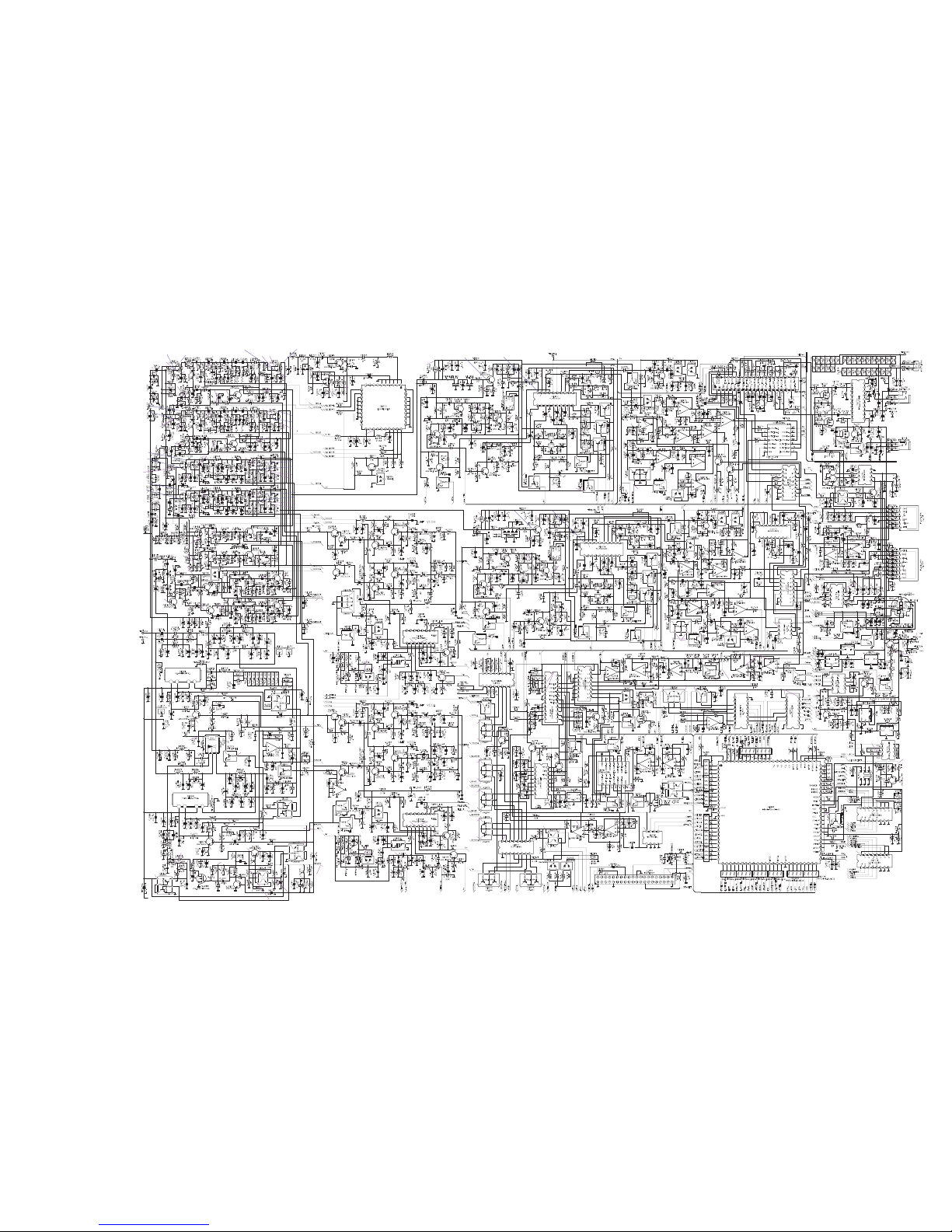
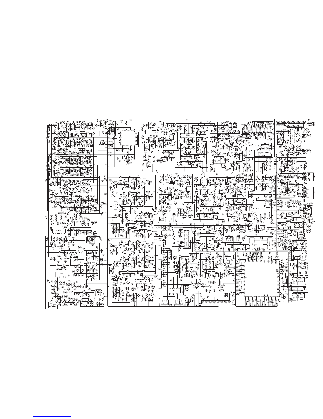
Circuit Diagram
19
MAIN Unit (Lot. 1~4)
FTM-350AR/E Technical Supplement
Parts Layout (Side A)
BA DCE
1
2
3
4
5
2SC4617 (BR)
(Q1302, 1315, 1326,
1602, 1883, 1893)
2SC5006 (24)
(Q1012, 1014, 1016,
1018, 1019, 1209,
1212, 1304, 1305,
1308, 1316, 1317,
1320, 1450, 1600)
2SC5277 (D2)
(Q1015)
2SC3356 (R24)
(Q1202)
2SC4915O (QO)
(Q1885)
DAN222 (N)
(D1028, 1466, 1616,
1860, 1861, 1862)
MB15A01PFV1
(Q1313, 1324)
DTC144EE (26)
(Q1323, 1327, 1464,
1603, 1607, 1615,
1801, 1866, 1888)
DA221 (26)
(D1309, 1321, 1325)
2SK296ZQ (ZQ)
(Q1002, 1007, 1008,
1009, 1010, 1011,
1013, 1301)
LM2904PWR
(Q1777)
LM2902PWR
(Q1473, 1622, 1881)
UMD5N
(Q1216, 1872)
2SB1132R (BA)
(Q1213)
UMX1N (X1)
(Q1214)
LV24100LP
(Q1303)
DTC114TE (04)
(Q1312)
NJM2552V
(Q1609)
DTA144EE (16)
(Q1458, 1463, 1612,
1614)
DTA114EE (14)
(Q1460, 1462, 1608,
1860)
UMG2N (G2)
(Q1617)
CD4066BPWR
(Q1471, 1892)
CD4053BPWR
(Q1472, 1620,
1865)
BU2090FS
(Q1862, 1877)
M62429FP
(Q1621)
UMA8N (A8)
(Q1861, 1873, 1874,
1875, 1876, 1878)
IMT17 (T17)
(Q1879)
TC7W53FU
(Q1898)
UMG8N (G8)
(Q1309)
M61529FP
(Q1469)
M24512-RDW6TP
(Q1775)
HD64F2268TF20
(Q1880)
CMX589AD5
(Q1864)
20
MAIN Unit (Lot. 1~4)
FTM-350AR/E Technical Supplement
Parts Layout (Side B)
ba dce
1
2
3
4
5
2SA1774 (FR)
(Q1314, 1325)
2SC4617 (BR)
(Q1454, 1465, 1468,
1475, 1616, 1754,
1756, 1757, 1770,
1776, 1863, 1867,
1890, 1895)
2SC5006 (24)
(Q1003, 1006, 1017,
1306, 1307, 1310,
1311, 1318, 1319,
1321, 1322)
2SC4915O (QO)
(Q1451, 1452, 1453,
1456, 1601, 1604,
1605, 1606,)
LM2904PWR
(Q1215, 1470,
1882, 1896)
TDA2822D
(Q1760)
LM2902PWR
(Q1474, 1623)
DTC144EE (26)
(Q1207, 1455,
1467,1618, 1753, 1763,
1768, 1891, 1897,
1900, 1901, 1902 )
DA221 (26)
(D1310, 1322, 1467, 1617)
MC2850 (A7)
(D1464, 1465, 1614, 1615)
DTC143EE (23)
(Q1205)
CD4094BPWR
(Q1870)
BU9253FS
(Q1619)
2SK296ZQ (ZQ)
(Q1001, 1004, 1005)
UMD5N
(Q1203, 1206, 1884)
RQA0004PXDQS (PX)
(Q1211)
2SB1132R (BA)
(Q1759)
UMX1N (X1)
(Q1758)
NJM2552V
(Q1457)
DTA144EE (16)
(Q1459, 1613, 1762)
DTA114EE (14)
(Q1611, 1869)
UMG2N (G2)
(Q1466)
CD4053BPWR
(Q1773, 1774)
M62353AGP
(Q1871)
CMX865AE4
(Q1887)
2SK397300L (5V)
(Q1750, 1751, 1752,
1889, 1899)
TDA1519CTH
(Q1755)
S-35190A
(Q1765)
BA09CC0FP
(Q1766)
NJM78M05DL1A
(Q1767)
2SB1301 (ZQ)
(Q1769)
S-80835CNMC
(Q1767)
UMA8N (A8)
(Q1868)
RA60H4047M1
(Q1201)
RA60H1317M1
(Q1208)
ADM101EARMZ
(Q1761)
XC6201P332MR (FR)
(Q1764, 1894)
21
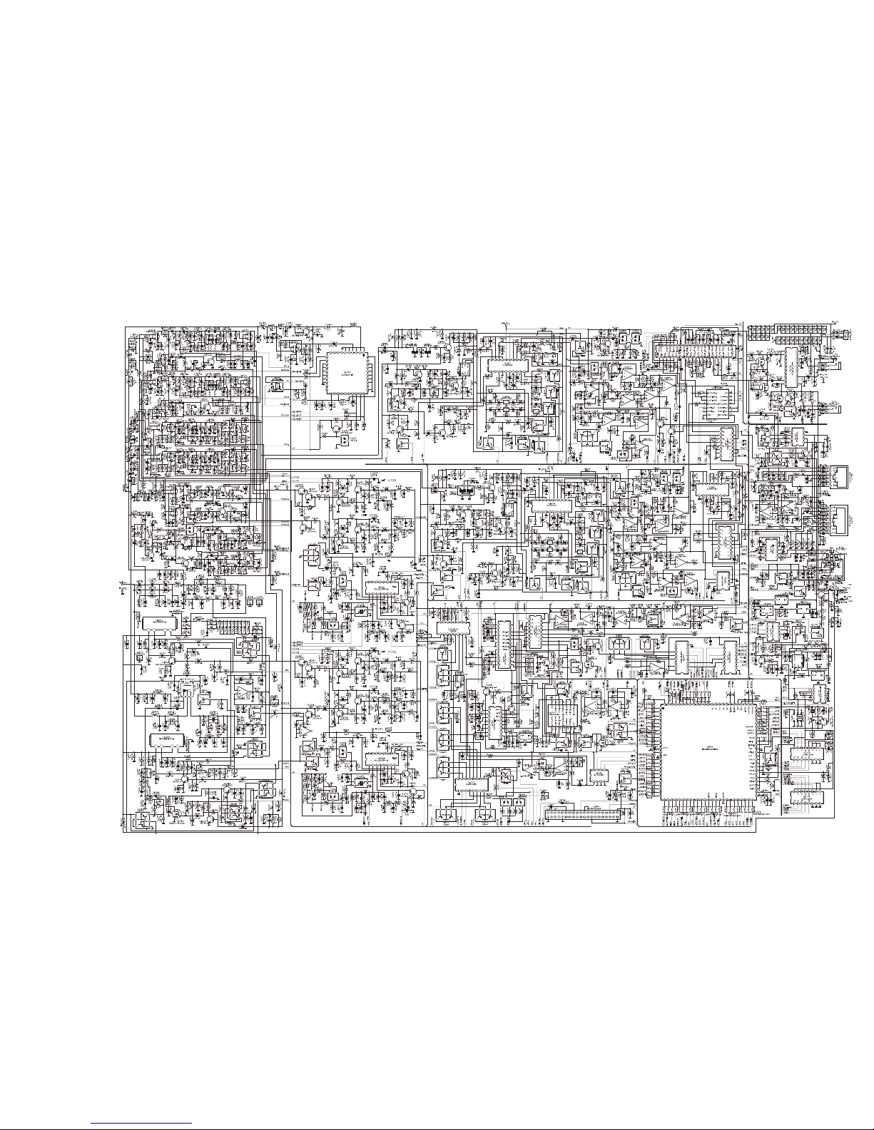
MAIN Unit (Lot. 5~)
FTM-350AR/E Technical Supplement
Circuit Diagram
25
MAIN Unit (Lot. 27~)
FTM-350AR/E Technical Supplement
Circuit Diagram
MAIN Unit
Parts List
REF DESCRIPTION VALUE V/W TOL. MFR'S DESIG VXSTD P/N VERS.
PCB with Components CS2062701 DST:USA, TYP:A2U
Printed Circuit Board FR018090F 1-4
BT1750 LI-ION BATTERY MS614SE FL28E Q9000884 1- A B3
C 1001 CHIP CAP. 0.001uF 50V B GRM155B11H102KA01D K22178809 1- B a2
C 1002 CHIP CAP. 2pF 50V CK GRM1554C1H2R0BZ01D K22178289 USA 1- B a2
C 1004 CHIP CAP. 0.001uF 50V B GRM155B11H102KA01D K22178809 1- B a2
C 1005 CHIP CAP. 0.001uF 50V B GRM155B11H102KA01D K22178809 1- A D2
C 1006 CHIP CAP. 68pF 50V CH GRM1552C1H680JZ01D K22178232 1- A D2
C 1007 CHIP CAP. 0.001uF 50V B GRM155B11H102KA01D K22178809 1- A C2
C 1008 CHIP CAP. 27pF 50V CH GRM1552C1H270JZ01D K22178222 1- A D2
C 1009 CHIP CAP. 0.5pF 50V CK GRM1554C1HR50BZ01D K22178285 1- A D2
C 1010 CHIP CAP. 0.5pF 50V CK GRM1554C1HR50BZ01D K22178285 1- A D2
C 1011 CHIP CAP. 27pF 50V CH GRM1552C1H270JZ01D K22178222 1- A D2
C 1012 CHIP CAP. 1pF 50V CK GRM1554C1H1R0BZ01D K22178287 1- A D2
C 1013 CHIP CAP. 0.75pF 50V CK GRM1554C1HR75BZ01D K22178286 1- A D2
C 1014 CHIP CAP. 0.5pF 50V CK GRM1554C1HR50BZ01D K22178285 1- A D2
C 1015 CHIP CAP. 1pF 50V CK GRM1554C1H1R0BZ01D K22178287 1- A D2
C 1016 CHIP CAP. 1pF 50V CK GRM1554C1H1R0BZ01D K22178287 1- A D2
C 1017 CHIP CAP. 27pF 50V CH GRM1552C1H270JZ01D K22178222 1- A D2
C 1018 CHIP CAP. 15pF 50V CH GRM1552C1H150GZ01 K22178300 1- A D3
C 1019 CHIP CAP. 0.01uF 25V B GRM155B11E103KA01D K22148834 1- A D3
C 1020 CHIP CAP. 12pF 50V CH GRM1552C1H120JZ01D K22178214 AUSTRALIA 1- B a2
C 1020 CHIP CAP. 12pF 50V CH GRM1552C1H120JZ01D K22178214 EUROPE 1- B a2
C 1020 CHIP CAP. 12pF 50V CH GRM1552C1H120JZ01D K22178214 EXPORT 1- B a2
C 1020 CHIP CAP. 33pF 50V CH GRM1552C1H330JZ01D K22178224 USA 1- B a2
C 1021 CHIP CAP. 3pF 50V CJ GRM1553C1H3R0BZ01D K22178290 1- B a2
C 1022 CHIP CAP. 0.001uF 50V B GRM155B11H102KA01D K22178809 1- B a2
C 1023 CHIP CAP. 0.001uF 50V B GRM155B11H102KA01D K22178809 1- B b2
C 1024 CHIP CAP. 0.001uF 50V B GRM155B11H102KA01D K22178809 1- B b2
C 1025 CHIP CAP. 7pF 50V CH GRM1552C1H7R0BZ01D K22178294 1- B b2
C 1026 CHIP CAP. 2pF 50V CK GRM1554C1H2R0BZ01D K22178289 1- B b2
C 1027 CHIP CAP. 5pF 50V CH GRM1552C1H5R0BZ01D K22178292 1- B b2
C 1028 CHIP CAP. 22pF 50V CH GRM1552C1H220GZ01D K22179707 1- B b2
C 1029 CHIP CAP. 0.5pF 50V CK GRM1554C1HR50BZ01D K22178285 1- B b2
C 1030 CHIP CAP. 0.001uF 50V B GRM155B11H102KA01D K22178809 1- A C3
C 1031 CHIP CAP. 0.001uF 50V B GRM155B11H102KA01D K22178809 1- A C3
C 1032 CHIP CAP. 2pF 50V CK GRM1554C1H2R0BZ01D K22178289 1- A C3
C 1033 CHIP CAP. 0.001uF 50V B GRM155B11H102KA01D K22178809 1- A D3
C 1034 CHIP CAP. 6pF 50V CH GRM1552C1H6R0BZ01D K22178293 1- A C2
C 1035 CHIP CAP. 0.001uF 50V B GRM155B11H102KA01D K22178809 1- B a2
C 1036 CHIP CAP. 0.001uF 50V B GRM155B11H102KA01D K22178809 1- B a2
C 1037 CHIP CAP. 0.001uF 50V B GRM155B11H102KA01D K22178809 1- B a2
C 1039 CHIP CAP. 0.001uF 50V B GRM155B11H102KA01D K22178809 1- B a2
C 1040 CHIP CAP. 0.001uF 50V B GRM155B11H102KA01D K22178809 1- B a2
C 1041 CHIP CAP. 68pF 50V CH GRM1552C1H680JZ01D K22178232 1- B a2
C 1042 CHIP CAP. 0.001uF 50V B GRM155B11H102KA01D K22178809 1- A D3
C 1043 CHIP CAP. 27pF 50V CH GRM1552C1H270JZ01D K22178222 1- B a2
C 1044 CHIP CAP. 2pF 50V CK GRM1554C1H2R0BZ01D K22178289 1- B a2
C 1045 CHIP CAP. 0.5pF 50V CK GRM1554C1HR50BZ01D K22178285 1- B a2
C 1046 CHIP CAP. 27pF 50V CH GRM1552C1H270JZ01D K22178222 1- B a2
C 1047 CHIP CAP. 1pF 50V CK GRM1554C1H1R0BZ01D K22178287 1- B a2
C 1048 CHIP CAP. 0.5pF 50V CK GRM1554C1HR50BZ01D K22178285 1- B a2
C 1049 CHIP CAP. 0.5pF 50V CK GRM1554C1HR50BZ01D K22178285 1- B a2
C 1050 CHIP CAP. 0.5pF 50V CK GRM1554C1HR50BZ01D K22178285 1- B a2
C 1051 CHIP CAP. 1pF 50V CK GRM1554C1H1R0BZ01D K22178287 1- B a2
C 1052 CHIP CAP. 27pF 50V CH GRM1552C1H270JZ01D K22178222 1- B a2
C 1053 CHIP CAP. 15pF 50V CH GRM1552C1H150GZ01 K22178300 1- B a2
C 1054 CHIP CAP. 0.01uF 25V B GRM155B11E103KA01D K22148834 1- B a2
CS2062704 DST:EXP, TYP:A1
CS2062705 DST:EXP, TYP:A2
CS2062706 DST:EXP, TYP:A3
CS2062707 DST:EU, TYP:B1
CS2062708 DST:EU, TYP:B2
CS2062709 DST:EXP, TYP:B3
CS2062710 DST:EU, TYP:C1
CS2062711 DST:EU, TYP:C2
CS2062712 DST:EXP, TYP:C3
CS2062713 DST:EU, TYP:D1
CS2062714 DST:EU, TYP:D2
CS2062715 DST:AUS, TYP:H1
CS2062716 DST:AUS, TYP:H2
FR018090G W/ CE LABEL 5-8
FR018090F
FR018090G 9FR018090H 27-
W/O CE LABEL
LOT
5-8
SIDE
LAY ADR
29FTM-350AR/E Technical Supplement

MAIN Unit
Parts List
REF DESCRIPTION VALUE V/W TOL. MFR'S DESIG VXSTD P/N VERS.
C 1055 CHIP CAP. 0.001uF 50V B GRM155B11H102KA01D K22178809 1- A C2
C 1056 CHIP CAP. 0.001uF 50V B GRM155B11H102KA01D K22178809 1- B a3
C 1057 CHIP CAP. 0.001uF 50V B GRM155B11H102KA01D K22178809 1- B a2
C 1058 CHIP CAP. 9pF 50V CH GRM1552C1H9R0BZ01D K22178296 1- B a2
C 1059 CHIP CAP. 2pF 50V CK GRM1554C1H2R0BZ01D K22178289 1- B a2
C 1060 CHIP CAP. 5pF 50V CH GRM1552C1H5R0BZ01D K22178292 1- B a2
C 1061 CHIP CAP. 22pF 50V CH GRM1552C1H220GZ01D K22179707 1- B a2
C 1062 CHIP CAP. 0.5pF 50V CK GRM1554C1HR50BZ01D K22178285 1- B a2
C 1063 CHIP CAP. 0.001uF 50V B GRM155B11H102KA01D K22178809 1- B a2
C 1064 CHIP CAP. 0.001uF 50V B GRM155B11H102KA01D K22178809 1- B a2
C 1065 CHIP CAP. 3pF 50V CJ GRM1553C1H3R0BZ01D K22178290 1- B a2
C 1066 CHIP CAP. 0.001uF 50V B GRM155B11H102KA01D K22178809 1- B a2
C 1067 CHIP CAP. 6pF 50V CH GRM1552C1H6R0BZ01D K22178293 1- B a2
C 1068 CHIP CAP. 12pF 50V CH GRM1552C1H120JZ01D K22178214 1- A C1
C 1069 CHIP CAP. 0.001uF 50V B GRM155B11H102KA01D K22178809 1- A C1
C 1070 CHIP CAP. 4pF 50V CH GRM1552C1H4R0BZ01D K22178291 AUSTRALIA 1- A C1
C 1070 CHIP CAP. 4pF 50V CH GRM1552C1H4R0BZ01D K22178291 EUROPE 1- A C1
C 1070 CHIP CAP. 4pF 50V CH GRM1552C1H4R0BZ01D K22178291 EXPORT 1- A C1
C 1070 CHIP CAP. 4pF 50V CH GRM1552C1H4R0BZ01D K22178291 USA 1- A C1
C 1071 CHIP CAP. 7pF 50V CH GRM1552C1H7R0BZ01D K22178294 1- A C1
C 1072 CHIP CAP. 0.001uF 50V B GRM155B11H102KA01D K22178809 1- A C1
C 1073 CHIP CAP. 0.1uF 10V B GRM155B11A104KA01D K22108802 1- A C1
C 1074 CHIP CAP. 0.001uF 50V B GRM155B11H102KA01D K22178809 1- A C2
C 1075 CHIP CAP. 0.5pF 50V CK GRM1554C1HR50BZ01D K22178285 1- A C2
C 1076 CHIP CAP. 0.001uF 50V B GRM155B11H102KA01D K22178809 1- A C2
C 1077 CHIP CAP. 8pF 50V CH GRM1552C1H8R0BZ01D K22178295 1- A C2
C 1078 CHIP CAP. 1.5pF 50V CK GRM1554C1H1R5BZ01D K22178288 1- A C2
C 1079 CHIP CAP. 47pF 50V CH GRM1552C1H470JZ01D K22178228 1- A C2
C 1080 CHIP CAP. 0.75pF 50V CK GRM1554C1HR75BZ01D K22178286 1- A C2
C 1081 CHIP CAP. 18pF 50V CH GRM1552C1H180JZ01D K22178218 1- A C2
C 1082 CHIP CAP. 2pF 50V CK GRM1554C1H2R0BZ01D K22178289 1- A C2
C 1083 CHIP CAP. 0.5pF 50V CK GRM1554C1HR50BZ01D K22178285 1- A C2
C 1084 CHIP CAP. 47pF 50V CH GRM1552C1H470JZ01D K22178228 1- A C2
C 1085 CHIP CAP. 8pF 50V CH GRM1552C1H8R0BZ01D K22178295 1- A C2
C 1086 CHIP CAP. 0.5pF 50V CK GRM1554C1HR50BZ01D K22178285 1- A C2
C 1087 CHIP CAP. 1pF 50V CK GRM1554C1H1R0BZ01D K22178287 1- A C3
C 1088 CHIP CAP. 47pF 50V CH GRM1552C1H470JZ01D K22178228 1- A C2
C 1089 CHIP CAP. 15pF 50V CH GRM1552C1H150GZ01 K22178300 AUSTRALIA 1- A C3
C 1089 CHIP CAP. 15pF 50V CH GRM1552C1H150GZ01 K22178300 EUROPE 1- A C3
C 1089 CHIP CAP. 15pF 50V CH GRM1552C1H150GZ01 K22178300 EXPORT 1- A C3
C 1089 CHIP CAP. 15pF 50V CH GRM1552C1H150GZ01 K22178300 USA 1- A C3
C 1090 CHIP CAP. 0.001uF 50V B GRM155B11H102KA01D K22178809 1- A C3
C 1091 CHIP CAP. 0.01uF 25V B GRM155B11E103KA01D K22148834 1- A C3
C 1092 CHIP CAP. 0.001uF 50V B GRM155B11H102KA01D K22178809 1- A C3
C 1093 CHIP CAP. 7pF 50V CH GRM1552C1H7R0BZ01D K22178294 1- A C3
C 1094 CHIP CAP. 12pF 50V CH GRM1552C1H120JZ01D K22178214 1- A C1
C 1095 CHIP CAP. 4pF 50V CH GRM1552C1H4R0BZ01D K22178291 1- A C1
C 1096 CHIP CAP. 10pF 50V CH GRM1552C1H100BZ01D K22178297 1- A C1
C 1097 CHIP CAP. 8pF 50V CH GRM1552C1H8R0DZ01D K22178210 1- A C1
C 1098 CHIP CAP. 15pF 50V CH GRM1552C1H150GZ01 K22178300 1- A C1
C 1099 CHIP CAP. 3pF 50V CJ GRM1553C1H3R0BZ01D K22178290 AUSTRALIA 1- A C1
C 1099 CHIP CAP. 3pF 50V CJ GRM1553C1H3R0BZ01D K22178290 EUROPE 1- A C1
C 1099 CHIP CAP. 3pF 50V CJ GRM1553C1H3R0BZ01D K22178290 EXPORT 1- A C1
C 1099 CHIP CAP. 3pF 50V CJ GRM1553C1H3R0BZ01D K22178290 USA 1- A C1
C 1100 CHIP CAP. 9pF 50V CH GRM1552C1H9R0BZ01D K22178296 AUSTRALIA 1- A C1
C 1100 CHIP CAP. 9pF 50V CH GRM1552C1H9R0BZ01D K22178296 EUROPE 1- A C1
C 1100 CHIP CAP. 9pF 50V CH GRM1552C1H9R0BZ01D K22178296 EXPORT 1- A C1
C 1100 CHIP CAP. 9pF 50V CH GRM1552C1H9R0BZ01D K22178296 USA 1- A C1
C 1101 CHIP CAP. 0.001uF 50V B GRM155B11H102KA01D K22178809 1- A C2
C 1102 CHIP CAP. 0.001uF 50V B GRM155B11H102KA01D K22178809 1- A C1
C 1103 CHIP CAP. 0.001uF 50V B GRM155B11H102KA01D K22178809 1- A C1
C 1104 CHIP CAP. 0.1uF 10V B GRM155B11A104KA01D K22108802 1- A C1
C 1105 CHIP CAP. 0.001uF 50V B GRM155B11H102KA01D K22178809 1- A D2
C 1106 CHIP CAP. 0.5pF 50V CK GRM1554C1HR50BZ01D K22178285 1- A D2
C 1107 CHIP CAP. 0.001uF 50V B GRM155B11H102KA01D K22178809 1- A D2
C 1108 CHIP CAP. 8pF 50V CH GRM1552C1H8R0BZ01D K22178295 1- A D2
C 1109 CHIP CAP. 0.75pF 50V CK GRM1554C1HR75BZ01D K22178286 1- A D2
C 1110 CHIP CAP. 47pF 50V CH GRM1552C1H470JZ01D K22178228 1- A D2
C 1111 CHIP CAP. 0.75pF 50V CK GRM1554C1HR75BZ01D K22178286 1- A D2
C 1112 CHIP CAP. 18pF 50V CH GRM1552C1H180JZ01D K22178218 1- A D2
C 1113 CHIP CAP. 1.5pF 50V CK GRM1554C1H1R5BZ01D K22178288 1- A D2
C 1114 CHIP CAP. 0.75pF 50V CK GRM1554C1HR75BZ01D K22178286 1- A D2
C 1115 CHIP CAP. 47pF 50V CH GRM1552C1H470JZ01D K22178228 1- A D2
C 1116 CHIP CAP. 8pF 50V CH GRM1552C1H8R0BZ01D K22178295 1- A D2
C 1117 CHIP CAP. 0.5pF 50V CK GRM1554C1HR50BZ01D K22178285 1- A D2
LOT
SIDE
LAY ADR
30 FTM-350AR/E Technical Supplement

MAIN Unit
Parts List
REF DESCRIPTION VALUE V/W TOL. VXSTD P/N VERS.
C 1118 CHIP CAP. 1pF 50V CK GRM1554C1H1R0BZ01D K22178287 1- A D2
C 1119 CHIP CAP. 47pF 50V CH GRM1552C1H470JZ01D K22178228 1- A D2
C 1120 CHIP CAP. 15pF 50V CH GRM1552C1H150GZ01 K22178300 AUSTRALIA 1- A D2
C 1120 CHIP CAP. 15pF 50V CH GRM1552C1H150GZ01 K22178300 EUROPE 1- A D2
C 1120 CHIP CAP. 15pF 50V CH GRM1552C1H150GZ01 K22178300 EXPORT 1- A D2
C 1120 CHIP CAP. 15pF 50V CH GRM1552C1H150GZ01 K22178300 USA 1- A D2
C 1121 CHIP CAP. 0.001uF 50V B GRM155B11H102KA01D K22178809 1- A D3
C 1122 CHIP CAP. 0.01uF 25V B GRM155B11E103KA01D K22148834 1- A D2
C 1123 CHIP CAP. 0.001uF 50V B GRM155B11H102KA01D K22178809 1- A D3
C 1124 CHIP CAP. 7pF 50V CH GRM1552C1H7R0BZ01D K22178294 1- A D3
C 1125 CHIP CAP. 30pF 50V CH GRM1552C1H300JZ01D K22178223 AUSTRALIA 1- A C1
C 1125 CHIP CAP. 30pF 50V CH GRM1552C1H300JZ01D K22178223 EUROPE 1- A C1
C 1125 CHIP CAP. 30pF 50V CH GRM1552C1H300JZ01D K22178223 EXPORT 1- A C1
C 1125 CHIP CAP. 30pF 50V CH GRM1552C1H300JZ01D K22178223 USA 1- A C1
C 1126 CHIP CAP. 4pF 50V CH GRM1552C1H4R0BZ01D K22178291 1- A C1
C 1127 CHIP CAP. 2pF 50V CK GRM1554C1H2R0BZ01D K22178289 1- A C1
C 1128 CHIP CAP. 22pF 50V CH GRM1552C1H220JZ01D K22178220 1- A C1
C 1129 CHIP CAP. 0.001uF 50V B GRM155B11H102KA01D K22178809 1- A C1
C 1130 CHIP CAP. 0.001uF 50V B GRM155B11H102KA01D K22178809 1- A C1
C 1131 CHIP CAP. 0.001uF 50V B GRM155B11H102KA01D K22178809 1- A C2
C 1132 CHIP CAP. 47pF 50V UJ GRM1553U1H470JZ01D K22178319 1- A C2
C 1133 CHIP CAP. 5pF 50V CH GRM1552C1H5R0BZ01D K22178292 1- A C2
C 1134 CHIP CAP. 2pF 50V CK GRM1554C1H2R0BZ01D K22178289 1- A C2
C 1135 CHIP CAP. 4pF 50V CH GRM1552C1H4R0BZ01D K22178291 1- A C2
C 1136 CHIP CAP. 27pF 50V CH GRM1552C1H270JZ01D K22178222 1- A C3
C 1137 CHIP CAP. 0.001uF 50V B GRM155B11H102KA01D K22178809 1- A C1
C 1138 CHIP CAP. 1pF 50V CK GRM1554C1H1R0BZ01D K22178287 1- A C3
C 1139 CHIP CAP. 0.001uF 50V B GRM155B11H102KA01D K22178809 1- A C3
C 1140 CHIP CAP. 10pF 50V CH GRM1552C1H100BZ01D K22178297 1- B a3
C 1141 CHIP CAP. 0.5pF 50V CK GRM1554C1HR50BZ01D K22178285 1- A C1
C 1142 CHIP CAP. 0.001uF 50V B GRM155B11H102KA01D K22178809 1- A C1
C 1143 CHIP CAP. 0.001uF 50V B GRM155B11H102KA01D K22178809 1- A D2
C 1144 CHIP CAP. 47pF 50V UJ GRM1553U1H470JZ01D K22178319 1- A D2
C 1145 CHIP CAP. 5pF 50V CH GRM1552C1H5R0BZ01D K22178292 1- A D2
C 1146 CHIP CAP. 2pF 50V CK GRM1554C1H2R0BZ01D K22178289 1- A D2
C 1147 CHIP CAP. 4pF 50V CH GRM1552C1H4R0BZ01D K22178291 1- A D2
C 1148 CHIP CAP. 22pF 50V CH GRM1552C1H220JZ01D K22178220 1- A D2
C 1149 CHIP CAP. 0.001uF 50V B GRM155B11H102KA01D K22178809 1- A C2
C 1150 CHIP CAP. 1pF 50V CK GRM1554C1H1R0BZ01D K22178287 1- A D3
C 1151 CHIP CAP. 0.001uF 50V B GRM155B11H102KA01D K22178809 1- A D3
C 1152 CHIP CAP. 10pF 50V CH GRM1552C1H100BZ01D K22178297 1- B a3
C 1153 CHIP CAP. 0.001uF 50V B GRM155B11H102KA01D K22178809 1- A D2
C 1154 CHIP CAP. 2pF 50V CK GRM1554C1H2R0BZ01D K22178289 1- B a1
C 1155 CHIP CAP. 2pF 200V CK GRM1884C2D2R0CV01D K22234204 1- B a1
C 1156 CHIP CAP. 220pF 50V CH GRM1552C1H221JA01D K22179713 1- A D1
C 1157 CHIP CAP. 2pF 50V CK GRM1554C1H2R0BZ01D K22178289 1- A D1
C 1158 CHIP CAP. 6pF 50V CH GRM1552C1H6R0BZ01D K22178293 1- A D1
C 1159 CHIP CAP. 0.001uF 50V B GRM155B11H102KA01D K22178809 1- A D1
C 1160 CHIP CAP. 2pF 50V CK GRM1554C1H2R0BZ01D K22178289 1- A D2
C 1161 CHIP CAP. 1.5pF 50V CK GRM1554C1H1R5BZ01D K22178288 1- A D1
C 1162 CHIP CAP. 8pF 50V CH GRM1552C1H8R0BZ01D K22178295 1- A D2
C 1163 CHIP CAP. 0.001uF 50V B GRM155B11H102KA01D K22178809 1- A D2
C 1164 CHIP CAP. 0.001uF 50V B GRM155B11H102KA01D K22178809 1- B b2
C 1166 CHIP CAP. 0.001uF 50V B GRM155B11H102KA01D K22178809 1- B a2
C 1167 CHIP CAP. 1pF 50V CK GRM1554C1H1R0BZ01D K22178287 1- B b2
C 1168 CHIP CAP. 22pF 50V CH GRM1552C1H220GZ01D K22179707 1- B a2
C 1169 CHIP CAP. 10pF 50V CH GRM1552C1H100BZ01D K22178297 1- B b2
C 1170 CHIP CAP. 10pF 50V CH GRM1552C1H100BZ01D K22178297 1- B b3
C 1171 CHIP CAP. 0.75pF 50V CK GRM1554C1HR75BZ01D K22178286 1- B b3
C 1172 CHIP CAP. 2pF 50V CK GRM1554C1H2R0BZ01D K22178289 1- B b3
C 1173 CHIP CAP. 2pF 50V CK GRM1554C1H2R0BZ01D K22178289 1- B b3
C 1174 CHIP CAP. 0.001uF 50V B GRM155B11H102KA01D K22178809 1- B b3
C 1175 CHIP CAP. 2pF 50V CK GRM1554C1H2R0BZ01D K22178289 1- A D1
C 1176 CHIP CAP. 8pF 50V CH GRM1552C1H8R0BZ01D K22178295 1- A D2
C 1177 CHIP CAP. 0.001uF 50V B GRM155B11H102KA01D K22178809 1- A D2
C 1179 CHIP CAP. 0.001uF 50V B GRM155B11H102KA01D K22178809 1- A E2
C 1180 CHIP CAP. 1pF 50V CK GRM1554C1H1R0BZ01D K22178287 1- A D2
C 1181 CHIP CAP. 22pF 50V CH GRM1552C1H220GZ01D K22179707 1- A D2
C 1182 CHIP CAP. 10pF 50V CH GRM1552C1H100BZ01D K22178297 1- A E2
C 1183 CHIP CAP. 15pF 50V CH GRM1552C1H150JZ01D K22178216 1- A D2
C 1184 CHIP CAP. 0.75pF 50V CK GRM1554C1HR75BZ01D K22178286 1- A E2
C 1185 CHIP CAP. 2pF 50V CK GRM1554C1H2R0BZ01D K22178289 1- A D2
C 1186 CHIP CAP. 2pF 50V CK GRM1554C1H2R0BZ01D K22178289 1- A D2
C 1187 CHIP CAP. 0.001uF 50V B GRM155B11H102KA01D K22178809 1- A E2
C 1188 CHIP CAP. 0.001uF 50V B GRM155B11H102KA01D K22178809 1- B a3
MFR'S DESIG
LOT
SIDE
LAY ADR
31FTM-350AR/E Technical Supplement

MAIN Unit
Parts List
REF DESCRIPTION VALUE V/W TOL. MFR'S DESIG VXSTD P/N VERS.
C 1189 CHIP CAP. 0.001uF 50V B GRM155B11H102KA01D K22178809 1- B a2
C 1190 CHIP CAP. 27pF 50V CH GRM1552C1H270JZ01D K22178222 1- B a2
C 1191 CHIP CAP. 27pF 50V CH GRM1552C1H270JZ01D K22178222 1- A D2
C 1192 CHIP CAP. 0.001uF 50V B GRM155B11H102KA01D K22178809 1- B b1
C 1193 CHIP CAP. 0.001uF 50V B GRM155B11H102KA01D K22178809 1- B b2
C 1194 CHIP CAP. 0.001uF 50V B GRM155B11H102KA01D K22178809 1- B a3
C 1195 CHIP CAP. 0.001uF 50V B GRM155B11H102KA01D K22178809 1- A C1
C 1196 CHIP CAP. 0.01uF 25V B GRM155B11E103KA01D K22148834 1- A C2
C 1198 CHIP CAP. 0.001uF 50V B GRM155B11H102KA01D K22178809 1- A B1
C 1199 CHIP CAP. 0.001uF 50V B GRM155B11H102KA01D K22178809 1- A D1
C 1200 CHIP CAP. 0.001uF 50V B GRM155B11H102KA01D K22178809 1- B a1
C 1201 CHIP CAP. 4pF 200V CH GRM1882C2D4R0CV01D K22234206 1- B a1
C 1202 CHIP CAP. 4pF 200V CH GRM1882C2D4R0CV01D K22234206 1- B a1
C 1204 CHIP CAP. 0.5pF 200V CK GRM1884C2DR50CY21D K22234201 1- B a1
C 1205 CHIP CAP. 2pF 200V CK GRM1884C2D2R0CV01D K22234204 1- B a1
C 1206 CHIP CAP. 2pF 200V CK GRM1884C2D2R0CV01D K22234204 1- B a1
C 1208 CHIP CAP. 4pF 200V CH GRM1882C2D4R0CV01D K22234206 1- B a1
C 1209 CHIP CAP. 4pF 200V CH GRM1882C2D4R0CV01D K22234206 1- B a1
C 1211 CHIP CAP. 3pF 200V CJ GRM1883C2D3R0CV01D K22234205 1- B a1
C 1213 CHIP CAP. 0.5pF 200V CK GRM1884C2DR50CY21D K22234201 1- B a1
C 1214 CHIP CAP. 9pF 50V CH GRM1552C1H9R0BZ01D K22178296 1- A D1
C 1215 CHIP CAP. 3pF 200V CJ GRM1883C2D3R0CV01D K22234205 1- B a1
C 1216 CHIP CAP. 1.5pF 200V CK GRM1884C2D1R5CV01D K22234213 1- B a1
C 1217 CHIP CAP. 0.001uF 50V B GRM155B11H102KA01D K22178809 1- A D1
C 1218 CHIP CAP. 4pF 200V CH GRM1882C2D4R0CV01D K22234206 1- B a1
C 1219 CHIP CAP. 4pF 200V CH GRM1882C2D4R0CV01D K22234206 1- B a1
C 1220 CHIP CAP. 0.001uF 50V B GRM155B11H102KA01D K22178809 1- A D1
C 1222 CHIP CAP. 2pF 200V CK GRM1884C2D2R0CV01D K22234204 1- B a1
C 1223 CHIP CAP. 0.5pF 200V CK GRM1884C2DR50CY21D K22234201 1- A D1
C 1224 CHIP CAP. 6pF 50V CH GRM1552C1H6R0BZ01D K22178293 1- A D1
C 1225 CHIP CAP. 0.001uF 50V B GRM155B11H102KA01D K22178809 1- B a1
C 1226 CHIP CAP. 0.0047uF 50V B GRM155B11H472KA01D K22178838 1- B a2
C 1227 CHIP CAP. 0.0047uF 50V B GRM155B11H472KA01D K22178838 1- B a2
C 1228 AL.ELECTRO.CAP. 22uF 50V EEE1HA220WP K48170026 1- A D2
C 1229 CHIP CAP. 7pF 50V CH GRM1552C1H7R0BZ01D K22178294 1- A D3
C 1230 CHIP CAP. 0.0047uF 50V B GRM155B11H472KA01D K22178838 1- B a2
C 1231 CHIP TA.CAP. 1uF 16V TEESVA1C105M8R K78120009 1- B a2
C 1232 CHIP CAP. 22pF 50V CH GRM1552C1H220JZ01D K22178220 1- A D3
C 1233 CHIP CAP. 0.001uF 50V B GRM155B11H102KA01D K22178809 1- A D3
C 1234 CHIP CAP. 0.001uF 50V B GRM155B11H102KA01D K22178809 1- A D3
C 1235 CHIP CAP. 0.01uF 25V B GRM155B11E103KA01D K22148834 1- B b3
C 1236 CHIP CAP. 47pF 50V CH GRM1552C1H470JZ01D K22178228 1- A C3
C 1237 CHIP CAP. 0.001uF 50V B GRM155B11H102KA01D K22178809 1- A C3
C 1239 CHIP CAP. 0.001uF 50V B GRM155B11H102KA01D K22178809 1- B b1
C 1240 CHIP CAP. 22pF 50V CH GRM1552C1H220JZ01D K22178220 1- A C1
C 1241 CHIP CAP. 15pF 200V CH GRM2192C2D150JV01D K22230218 1- B a1
C 1242 CHIP CAP. 22pF 50V CH GRM1552C1H220JZ01D K22178220 1- A C1
C 1243 CHIP CAP. 12pF 200V CH GRM2192C2D120JV01D K22230217 1- B a1
C 1244 CHIP CAP. 4pF 200V CH GRM1882C2D4R0CV01D K22234206 1- B b1
C 1245 CHIP CAP. 0.001uF 50V B GRM155B11H102KA01D K22178809 1- B b1
C 1246 CHIP CAP. 0.001uF 50V B GRM155B11H102KA01D K22178809 1- A C1
C 1248 CHIP CAP. 0.01uF 25V B GRM155B11E103KA01D K22148834 1- A C1
C 1249 CHIP CAP. 0.001uF 50V B GRM155B11H102KA01D K22178809 1- B b1
C 1250 CHIP CAP. 0.1uF 10V B GRM155B11A104KA01D K22108802 1- B b1
C 1251 CHIP CAP. 0.01uF 25V B GRM155B11E103KA01D K22148834 1- B b1
C 1252 CHIP CAP. 0.001uF 50V B GRM155B11H102KA01D K22178809 1- B b1
C 1253 CHIP CAP. 0.001uF 50V B GRM155B11H102KA01D K22178809 1- B b3
C 1254 CHIP TA.CAP. 10uF 10V TEESVA1A106M8R K78100028 1- A D1
C 1255 CHIP CAP. 0.047uF 10V B GRM155B11A473KA01D K22108801 1- B b1
C 1256 CHIP CAP. 0.5pF 200V CK GRM1884C2DR50CY21D K22234201 1- B b1
C 1257 CHIP CAP. 18pF 200V CH GRM2192C2D180JV01D K22230219 1- B b1
C 1258 CHIP CAP. 6pF 50V CH GRM1552C1H6R0BZ01D K22178293 1- B b1
C 1259 CHIP CAP. 18pF 200V CH GRM2192C2D180JV01D K22230219 1- B b1
C 1260 CHIP CAP. 8pF 200V CH GRM2192C2D8R0DY21D K22230214 1-6 B b1
C 1260 CHIP CAP. 6pF 200V CH GRM2192C2D6R0DY21D K22230212 7- B b1
C 1261 CHIP CAP. 0.001uF 50V B GRM155B11H102KA01D K22178809 1- B b1
C 1262 CHIP CAP. 8pF 200V CH GRM2192C2D8R0DY21D K22230214 1- B b1
C 1263 CHIP CAP. 8pF 200V CH GRM2192C2D8R0DY21D K22230214 1- B b1
C 1264 CHIP CAP. 0.001uF 50V B GRM155B11H102KA01D K22178809 1- B b1
C 1265 CHIP CAP. 0.5pF 200V CK GRM1884C2DR50CY21D K22234201 1- B b1
C 1266 CHIP CAP. 7pF 50V CH GRM1552C1H7R0BZ01D K22178294 1- B b1
C 1267 CHIP CAP. 0.001uF 50V B GRM155B11H102KA01D K22178809 1- B b1
C 1268 CHIP CAP. 0.0047uF 50V B GRM155B11H472KA01D K22178838 1- B c1
C 1269 CHIP CAP. 15pF 50V CH GRM1552C1H150JZ01D K22178216 1- A C1
C 1270 CHIP CAP. 33pF 50V CH GRM1552C1H330JZ01D K22178224 1- A C1
LOT
SIDE
LAY ADR
32 FTM-350AR/E Technical Supplement
 Loading...