


XILINX XC4062XL-2BG560I, XC4062XL-2BG560C, XC4062XL-2BG475I, XC4062XL-2BG475C, XC4062XL-2BG432I Datasheet
...0
R
XC4000E and XC4000X Series Field
Programmable Gate Arrays
May 14, 1999 (Version 1.6) |
0 |
0* |
Product Specification |
|
|
|
|
XC4000E and XC4000X Series
Features
Note: Information in this data sheet covers the XC4000E, XC4000EX, and XC4000XL families. A separate data sheet covers the XC4000XLA and XC4000XV families. Electrical Specifications and package/pin information are covered in separate sections for each family to make the information easier to access, review, and print. For access to these sections, see the Xilinx WEBLINX web site at
http://www.xilinx.com/partinfo/databook.htm#xc4000.
•System featured Field-Programmable Gate Arrays
-Select-RAMTM memory: on-chip ultra-fast RAM with
-synchronous write option
-dual-port RAM option
-Fully PCI compliant (speed grades -2 and faster)
-Abundant flip-flops
-Flexible function generators
-Dedicated high-speed carry logic
-Wide edge decoders on each edge
-Hierarchy of interconnect lines
-Internal 3-state bus capability
-Eight global low-skew clock or signal distribution networks
•System Performance beyond 80 MHz
•Flexible Array Architecture
•Low Power Segmented Routing Architecture
•Systems-Oriented Features
-IEEE 1149.1-compatible boundary scan logic support
-Individually programmable output slew rate
-Programmable input pull-up or pull-down resistors
-12 mA sink current per XC4000E output
•Configured by Loading Binary File
-Unlimited re-programmability
•Read Back Capability
-Program verification
-Internal node observability
•Backward Compatible with XC4000 Devices
•Development System runs on most common computer platforms
-Interfaces to popular design environments
-Fully automatic mapping, placement and routing
-Interactive design editor for design optimization
Low-Voltage Versions Available
•Low-Voltage Devices Function at 3.0 - 3.6 Volts
•XC4000XL: High Performance Low-Voltage Versions of XC4000EX devices
Additional XC4000X Series Features
•Highest Performance — 3.3 V XC4000XL
•Highest Capacity — Over 180,000 Usable Gates
•5 V tolerant I/Os on XC4000XL
•0.35 μm SRAM process for XC4000XL
•Additional Routing Over XC4000E
-almost twice the routing capacity for high-density designs
•Buffered Interconnect for Maximum Speed Blocks
•Improved VersaRingTM I/O Interconnect for Better Fixed
Pinout Flexibility |
6 |
•12 mA Sink Current Per XC4000X Output
•Flexible New High-Speed Clock Network
-Eight additional Early Buffers for shorter clock delays
-Virtually unlimited number of clock signals
•Optional Multiplexer or 2-input Function Generator on Device Outputs
•Four Additional Address Bits in Master Parallel Configuration Mode
•XC4000XV Family offers the highest density with 0.25 μm 2.5 V technology
Introduction
XC4000 Series high-performance, high-capacity Field Programmable Gate Arrays (FPGAs) provide the benefits of custom CMOS VLSI, while avoiding the initial cost, long development cycle, and inherent risk of a conventional masked gate array.
The result of thirteen years of FPGA design experience and feedback from thousands of customers, these FPGAs combine architectural versatility, on-chip Select-RAM memory with edge-triggered and dual-port modes, increased speed, abundant routing resources, and new, sophisticated software to achieve fully automated implementation of complex, high-density, high-performance designs.
The XC4000E and XC4000X Series currently have 20 members, as shown in Table 1.
May 14, 1999 (Version 1.6) |
6-5 |

R
XC4000E and XC4000X Series Field Programmable Gate Arrays
Table 1: XC4000E and XC4000X Series Field Programmable Gate Arrays
|
|
Max Logic |
Max. RAM |
Typical |
|
|
Number |
|
||
|
Logic |
Gates |
Bits |
Gate Range |
CLB |
Total |
of |
Max. |
||
Device |
Cells |
(No RAM) |
(No Logic) |
(Logic and RAM)* |
Matrix |
CLBs |
Flip-Flops |
User I/O |
||
|
|
|
|
|
|
|
|
|
|
|
XC4002XL |
152 |
1,600 |
2,048 |
1,000 |
- 3,000 |
8 x 8 |
64 |
256 |
64 |
|
|
|
|
|
|
|
|
|
|
|
|
XC4003E |
238 |
3,000 |
3,200 |
2,000 |
- 5,000 |
10 x 10 |
100 |
360 |
80 |
|
|
|
|
|
|
|
|
|
|
|
|
XC4005E/XL |
466 |
5,000 |
6,272 |
3,000 |
- 9,000 |
14 x 14 |
196 |
616 |
112 |
|
|
|
|
|
|
|
|
|
|
|
|
XC4006E |
608 |
6,000 |
8,192 |
4,000 |
- 12,000 |
16 x 16 |
256 |
768 |
128 |
|
|
|
|
|
|
|
|
|
|
|
|
XC4008E |
770 |
8,000 |
10,368 |
6,000 |
- 15,000 |
18 x 18 |
324 |
936 |
144 |
|
|
|
|
|
|
|
|
|
|
|
|
XC4010E/XL |
950 |
10,000 |
12,800 |
7,000 |
- 20,000 |
20 x 20 |
400 |
1,120 |
160 |
|
|
|
|
|
|
|
|
|
|
|
|
XC4013E/XL |
1368 |
13,000 |
18,432 |
10,000 |
- 30,000 |
24 x 24 |
576 |
1,536 |
192 |
|
|
|
|
|
|
|
|
|
|
|
|
XC4020E/XL |
1862 |
20,000 |
25,088 |
13,000 |
- 40,000 |
28 x 28 |
784 |
2,016 |
224 |
|
|
|
|
|
|
|
|
|
|
|
|
XC4025E |
2432 |
25,000 |
32,768 |
15,000 |
- 45,000 |
32 x 32 |
1,024 |
2,560 |
256 |
|
|
|
|
|
|
|
|
|
|
|
|
XC4028EX/XL |
2432 |
28,000 |
32,768 |
18,000 |
- 50,000 |
32 x 32 |
1,024 |
2,560 |
256 |
|
|
|
|
|
|
|
|
|
|
|
|
XC4036EX/XL |
3078 |
36,000 |
41,472 |
22,000 |
- 65,000 |
36 x 36 |
1,296 |
3,168 |
288 |
|
|
|
|
|
|
|
|
|
|
|
|
XC4044XL |
3800 |
44,000 |
51,200 |
27,000 |
- 80,000 |
40 x 40 |
1,600 |
3,840 |
320 |
|
|
|
|
|
|
|
|
|
|
|
|
XC4052XL |
4598 |
52,000 |
61,952 |
33,000 |
- 100,000 |
44 x 44 |
1,936 |
4,576 |
352 |
|
|
|
|
|
|
|
|
|
|
|
|
XC4062XL |
5472 |
62,000 |
73,728 |
40,000 |
- 130,000 |
48 x 48 |
2,304 |
5,376 |
384 |
|
|
|
|
|
|
|
|
|
|
|
|
XC4085XL |
7448 |
85,000 |
100,352 |
55,000 |
- 180,000 |
56 x 56 |
3,136 |
7,168 |
448 |
|
|
|
|
|
|
|
|
|
|
|
|
* Max values of Typical Gate Range include 20-30% of CLBs used as RAM.
Note: All functionality in low-voltage families is the same as in the corresponding 5-Volt family, except where numerical references are made to timing or power.
Description
XC4000 Series devices are implemented with a regular, flexible, programmable architecture of Configurable Logic Blocks (CLBs), interconnected by a powerful hierarchy of versatile routing resources, and surrounded by a perimeter of programmable Input/Output Blocks (IOBs). They have generous routing resources to accommodate the most complex interconnect patterns.
The devices are customized by loading configuration data into internal memory cells. The FPGA can either actively read its configuration data from an external serial or byte-parallel PROM (master modes), or the configuration data can be written into the FPGA from an external device (slave and peripheral modes).
XC4000 Series FPGAs are supported by powerful and sophisticated software, covering every aspect of design from schematic or behavioral entry, floor planning, simulation, automatic block placement and routing of interconnects, to the creation, downloading, and readback of the configuration bit stream.
Because Xilinx FPGAs can be reprogrammed an unlimited number of times, they can be used in innovative designs
where hardware is changed dynamically, or where hardware must be adapted to different user applications. FPGAs are ideal for shortening design and development cycles, and also offer a cost-effective solution for production rates well beyond 5,000 systems per month. For lowest high-volume unit cost, a design can first be implemented in the XC4000E or XC4000X, then migrated to one of Xilinx’ compatible HardWire mask-programmed devices.
Taking Advantage of Re-configuration
FPGA devices can be re-configured to change logic function while resident in the system. This capability gives the system designer a new degree of freedom not available with any other type of logic.
Hardware can be changed as easily as software. Design updates or modifications are easy, and can be made to products already in the field. An FPGA can even be re-con- figured dynamically to perform different functions at different times.
Re-configurable logic can be used to implement system self-diagnostics, create systems capable of being re-con- figured for different environments or operations, or implement multi-purpose hardware for a given application. As an added benefit, using re-configurable FPGA devices simplifies hardware design and debugging and shortens product time-to-market.
6-6 |
May 14, 1999 (Version 1.6) |

R
XC4000E and XC4000X Series Field Programmable Gate Arrays
XC4000E and XC4000X Series Compared to the XC4000
For readers already familiar with the XC4000 family of Xilinx Field Programmable Gate Arrays, the major new features in the XC4000 Series devices are listed in this section. The biggest advantages of XC4000E and XC4000X devices are significantly increased system speed, greater capacity, and new architectural features, particularly Select-RAM memory. The XC4000X devices also offer many new routing features, including special high-speed clock buffers that can be used to capture input data with minimal delay.
Any XC4000E device is pinoutand bitstream-compatible with the corresponding XC4000 device. An existing XC4000 bitstream can be used to program an XC4000E device. However, since the XC4000E includes many new features, an XC4000E bitstream cannot be loaded into an XC4000 device.
XC4000X Series devices are not bitstream-compatible with equivalent array size devices in the XC4000 or XC4000E families. However, equivalent array size devices, such as the XC4025, XC4025E, XC4028EX, and XC4028XL, are pinout-compatible.
Improvements in XC4000E and XC4000X
Increased System Speed
XC4000E and XC4000X devices can run at synchronous system clock rates of up to 80 MHz, and internal performance can exceed 150 MHz. This increase in performance over the previous families stems from improvements in both device processing and system architecture. XC4000 Series devices use a sub-micron multi-layer metal process. In addition, many architectural improvements have been made, as described below.
The XC4000XL family is a high performance 3.3V family based on 0.35μ SRAM technology and supports system speeds to 80 MHz.
PCI Compliance
XC4000 Series -2 and faster speed grades are fully PCI compliant. XC4000E and XC4000X devices can be used to implement a one-chip PCI solution.
Carry Logic
The speed of the carry logic chain has increased dramatically. Some parameters, such as the delay on the carry chain through a single CLB (TBYP), have improved by as
much as 50% from XC4000 values. See “Fast Carry Logic” on page 18 for more information.
Select-RAM Memory: Edge-Triggered, Synchro-
nous RAM Modes
The RAM in any CLB can be configured for synchronous, edge-triggered, write operation. The read operation is not affected by this change to an edge-triggered write.
Dual-Port RAM
A separate option converts the 16x2 RAM in any CLB into a 16x1 dual-port RAM with simultaneous Read/Write.
The function generators in each CLB can be configured as either level-sensitive (asynchronous) single-port RAM, edge-triggered (synchronous) single-port RAM, edge-trig- gered (synchronous) dual-port RAM, or as combinatorial logic.
Configurable RAM Content
The RAM content can now be loaded at configuration time, so that the RAM starts up with user-defined data.
H Function Generator
6
In current XC4000 Series devices, the H function generator is more versatile than in the original XC4000. Its inputs can come not only from the F and G function generators but also from up to three of the four control input lines. The H function generator can thus be totally or partially independent of the other two function generators, increasing the maximum capacity of the device.
IOB Clock Enable
The two flip-flops in each IOB have a common clock enable input, which through configuration can be activated individually for the input or output flip-flop or both. This clock enable operates exactly like the EC pin on the XC4000 CLB. This new feature makes the IOBs more versatile, and avoids the need for clock gating.
Output Drivers
The output pull-up structure defaults to a TTL-like totem-pole. This driver is an n-channel pull-up transistor, pulling to a voltage one transistor threshold below Vcc, just like the XC4000 family outputs. Alternatively, XC4000 Series devices can be globally configured with CMOS outputs, with p-channel pull-up transistors pulling to Vcc. Also, the configurable pull-up resistor in the XC4000 Series is a p-channel transistor that pulls to Vcc, whereas in the original XC4000 family it is an n-channel transistor that pulls to a voltage one transistor threshold below Vcc.
May 14, 1999 (Version 1.6) |
6-7 |
R
XC4000E and XC4000X Series Field Programmable Gate Arrays
Input Thresholds
The input thresholds of 5V devices can be globally configured for either TTL (1.2 V threshold) or CMOS (2.5 V threshold), just like XC2000 and XC3000 inputs. The two global adjustments of input threshold and output level are independent of each other. The XC4000XL family has an input threshold of 1.6V, compatible with both 3.3V CMOS and TTL levels.
Additional Improvements in XC4000X Only
Increased Routing
New interconnect in the XC4000X includes twenty-two additional vertical lines in each column of CLBs and twelve new horizontal lines in each row of CLBs. The twelve “Quad Lines” in each CLB row and column include optional repowering buffers for maximum speed. Additional high-perfor- mance routing near the IOBs enhances pin flexibility.
Global Signal Access to Logic
There is additional access from global clocks to the F and G function generator inputs.
Configuration Pin Pull-Up Resistors
During configuration, these pins have weak pull-up resistors. For the most popular configuration mode, Slave Serial, the mode pins can thus be left unconnected. The three mode inputs can be individually configured with or without weak pull-up or pull-down resistors. A pull-down resistor value of 4.7 kΩ is recommended.
The three mode inputs can be individually configured with or without weak pull-up or pull-down resistors after configuration.
The PROGRAM input pin has a permanent weak pull-up.
Faster Input and Output
A fast, dedicated early clock sourced by global clock buffers is available for the IOBs. To ensure synchronization with the regular global clocks, a Fast Capture latch driven by the early clock is available. The input data can be initially loaded into the Fast Capture latch with the early clock, then transferred to the input flip-flop or latch with the low-skew global clock. A programmable delay on the input can be used to avoid hold-time requirements. See “IOB Input Signals” on page 20 for more information.
Latch Capability in CLBs
Storage elements in the XC4000X CLB can be configured as either flip-flops or latches. This capability makes the FPGA highly synthesis-compatible.
Soft Start-up
Like the XC3000A, XC4000 Series devices have “Soft Start-up.” When the configuration process is finished and the device starts up, the first activation of the outputs is automatically slew-rate limited. This feature avoids potential ground bounce when all outputs are turned on simultaneously. Immediately after start-up, the slew rate of the individual outputs is, as in the XC4000 family, determined by the individual configuration option.
IOB Output MUX From Output Clock
A multiplexer in the IOB allows the output clock to select either the output data or the IOB clock enable as the output to the pad. Thus, two different data signals can share a single output pad, effectively doubling the number of device outputs without requiring a larger, more expensive package. This multiplexer can also be configured as an AND-gate to implement a very fast pin-to-pin path. See “IOB Output Signals” on page 23 for more information.
XC4000 and XC4000A Compatibility
Existing XC4000 bitstreams can be used to configure an XC4000E device. XC4000A bitstreams must be recompiled for use with the XC4000E due to improved routing resources, although the devices are pin-for-pin compatible.
Additional Address Bits
Larger devices require more bits of configuration data. A daisy chain of several large XC4000X devices may require a PROM that cannot be addressed by the eighteen address bits supported in the XC4000E. The XC4000X Series therefore extends the addressing in Master Parallel configuration mode to 22 bits.
6-8 |
May 14, 1999 (Version 1.6) |
R
XC4000E and XC4000X Series Field Programmable Gate Arrays
Detailed Functional Description
XC4000 Series devices achieve high speed through advanced semiconductor technology and improved architecture. The XC4000E and XC4000X support system clock rates of up to 80 MHz and internal performance in excess of 150 MHz. Compared to older Xilinx FPGA families, XC4000 Series devices are more powerful. They offer on-chip edge-triggered and dual-port RAM, clock enables on I/O flip-flops, and wide-input decoders. They are more versatile in many applications, especially those involving RAM. Design cycles are faster due to a combination of increased routing resources and more sophisticated software.
Basic Building Blocks
Xilinx user-programmable gate arrays include two major configurable elements: configurable logic blocks (CLBs) and input/output blocks (IOBs).
•CLBs provide the functional elements for constructing the user’s logic.
•IOBs provide the interface between the package pins and internal signal lines.
Three other types of circuits are also available:
•3-State buffers (TBUFs) driving horizontal longlines are associated with each CLB.
•Wide edge decoders are available around the periphery of each device.
•An on-chip oscillator is provided.
Programmable interconnect resources provide routing paths to connect the inputs and outputs of these configurable elements to the appropriate networks.
The functionality of each circuit block is customized during configuration by programming internal static memory cells. The values stored in these memory cells determine the logic functions and interconnections implemented in the FPGA. Each of these available circuits is described in this section.
Configurable Logic Blocks (CLBs)
Configurable Logic Blocks implement most of the logic in an FPGA. The principal CLB elements are shown in Figure 1. Two 4-input function generators (F and G) offer unrestricted versatility. Most combinatorial logic functions need four or fewer inputs. However, a third function generator (H) is provided. The H function generator has three inputs. Either zero, one, or two of these inputs can be the outputs of F and G; the other input(s) are from outside the CLB. The CLB can, therefore, implement certain functions of up to nine variables, like parity check or expand- able-identity comparison of two sets of four inputs.
Each CLB contains two storage elements that can be used to store the function generator outputs. However, the storage elements and function generators can also be used independently. These storage elements can be configured as flip-flops in both XC4000E and XC4000X devices; in the XC4000X they can optionally be configured as latches. DIN can be used as a direct input to either of the two storage elements. H1 can drive the other through the H function generator. Function generator outputs can also drive two outputs independent of the storage element outputs. This versatility increases logic capacity and simplifies routing.
Thirteen CLB inputs and four CLB outputs provide access to the function generators and storage elements. These inputs and outputs connect to the programmable interconnect resources outside the block.
Function Generators
Four independent inputs are provided to each of two func- |
|
tion generators (F1 - F4 and G1 - G4). These function gen- |
|
erators, with outputs labeled F’ and G’, are each capable of |
|
implementing any arbitrarily defined Boolean function of |
|
four inputs. The function generators are implemented as |
|
memory look-up tables. The propagation delay is therefore |
6 |
independent of the function implemented. |
A third function generator, labeled H’, can implement any Boolean function of its three inputs. Two of these inputs can optionally be the F’ and G’ functional generator outputs. Alternatively, one or both of these inputs can come from outside the CLB (H2, H0). The third input must come from outside the block (H1).
Signals from the function generators can exit the CLB on two outputs. F’ or H’ can be connected to the X output. G’ or H’ can be connected to the Y output.
A CLB can be used to implement any of the following functions:
•any function of up to four variables, plus any second function of up to four unrelated variables, plus any third function of up to three unrelated variables1
•any single function of five variables
•any function of four variables together with some functions of six variables
•some functions of up to nine variables.
Implementing wide functions in a single block reduces both the number of blocks required and the delay in the signal path, achieving both increased capacity and speed.
The versatility of the CLB function generators significantly improves system speed. In addition, the design-software tools can deal with each function generator independently. This flexibility improves cell usage.
1.When three separate functions are generated, one of the function outputs must be captured in a flip-flop internal to the CLB. Only two unregistered function generator outputs are available from the CLB.
May 14, 1999 (Version 1.6) |
6-9 |
R
XC4000E and XC4000X Series Field Programmable Gate Arrays
C1 • • • C 4 |
4 |
|
|
|
|
|
|
|
|
|
|
|
|
|
H1 |
|
DIN/H2 |
SR/H0 |
EC |
|
G4 |
|
|
|
|
S/R |
Bypass |
|
|
|
|
|
CONTROL |
|
G3 |
LOGIC |
|
DIN |
|
|
YQ |
|
F' |
|
D |
SD |
||
|
FUNCTION G' |
|
G' |
|
Q |
|
G2 |
OF |
|
H' |
|
|
|
G1-G4 |
|
|
|
|
||
|
|
|
|
|
||
G1 |
|
|
|
|
|
|
|
LOGIC |
|
|
|
EC |
|
|
FUNCTION |
|
|
RD |
||
|
G' |
|
|
|||
|
OF |
|
|
|
||
|
H' |
|
|
|
||
|
H' |
|
|
|
||
|
|
|
|
|
||
|
F', G', |
|
|
1 |
|
|
|
AND |
|
|
|
|
|
|
|
|
|
|
Y |
|
|
H1 |
|
|
|
|
|
|
|
|
|
|
|
|
F4 |
|
|
|
|
S/R |
Bypass |
|
|
|
|
|
|
|
|
|
|
DIN |
|
CONTROL |
XQ |
F3 |
LOGIC |
|
|
|
||
|
F' |
|
D |
SD |
||
|
FUNCTION F' |
|
G' |
|
Q |
|
F2 |
OF |
|
H' |
|
|
|
F1-F4 |
|
|
|
|
||
|
|
|
|
|
||
F1 |
|
|
|
|
|
|
|
|
|
|
|
EC |
RD |
K |
|
|
|
|
|
|
|
|
|
|
|
|
|
(CLOCK) |
|
|
|
|
1 |
|
|
|
|
H' |
|
|
X |
|
|
|
F' |
|
|
|
|
|
|
|
|
|
|
Multiplexer Controlled
by Configuration Program
X6692
Figure 1: Simplified Block Diagram of XC4000 Series CLB (RAM and Carry Logic functions not shown)
Flip-Flops
The CLB can pass the combinatorial output(s) to the interconnect network, but can also store the combinatorial results or other incoming data in one or two flip-flops, and connect their outputs to the interconnect network as well.
The two edge-triggered D-type flip-flops have common clock (K) and clock enable (EC) inputs. Either or both clock inputs can also be permanently enabled. Storage element functionality is described in Table 2.
Latches (XC4000X only)
The CLB storage elements can also be configured as latches. The two latches have common clock (K) and clock enable (EC) inputs. Storage element functionality is described in Table 2.
Clock Input
Each flip-flop can be triggered on either the rising or falling clock edge. The clock pin is shared by both storage elements. However, the clock is individually invertible for each storage element. Any inverter placed on the clock input is automatically absorbed into the CLB.
Clock Enable
The clock enable signal (EC) is active High. The EC pin is shared by both storage elements. If left unconnected for either, the clock enable for that storage element defaults to the active state. EC is not invertible within the CLB.
Table 2: CLB Storage Element Functionality (active rising edge is shown)
Mode |
K |
|
EC |
SR |
D |
Q |
||||
|
|
|
|
|
|
|
|
|
||
Power-Up or |
X |
|
X |
X |
X |
SR |
||||
GSR |
|
|||||||||
|
|
|
|
|
|
|
|
|||
|
|
|
|
|
|
|
|
|
||
|
|
|
X |
|
X |
1 |
X |
SR |
||
|
|
|
|
|
|
|
|
|
||
Flip-Flop |
__/ |
|
|
|
1* |
0* |
D |
D |
||
|
|
|
||||||||
|
|
|
|
|
|
|
|
|
|
|
|
|
|
0 |
|
|
|
X |
0* |
X |
Q |
|
|
|
|
|
|
|
|
|
|
|
Latch |
1 |
|
|
|
1* |
0* |
X |
Q |
||
|
|
|
|
|
|
|
|
|||
0 |
|
|
|
1* |
0* |
D |
D |
|||
|
|
|
|
|
|
|||||
|
|
|
|
|
|
|
||||
Both |
X |
|
0 |
0* |
X |
Q |
||||
|
|
|
|
|
|
|
|
|
||
Legend: |
|
|
|
|
|
|
|
|
||
X |
Don’t care |
|
|
|
|
|||||
__/ |
|
|
Rising edge |
|
|
|
|
|||
SR |
Set or Reset value. Reset is default. |
|
||||||||
0* |
|
|
Input is Low or unconnected (default value) |
|||||||
1* |
|
|
Input is High or unconnected (default value) |
|||||||
6-10 |
May 14, 1999 (Version 1.6) |
R
XC4000E and XC4000X Series Field Programmable Gate Arrays
Set/Reset
An asynchronous storage element input (SR) can be configured as either set or reset. This configuration option determines the state in which each flip-flop becomes operational after configuration. It also determines the effect of a Global Set/Reset pulse during normal operation, and the effect of a pulse on the SR pin of the CLB. All three set/reset functions for any single flip-flop are controlled by the same configuration data bit.
The set/reset state can be independently specified for each flip-flop. This input can also be independently disabled for either flip-flop.
The set/reset state is specified by using the INIT attribute, or by placing the appropriate set or reset flip-flop library symbol.
SR is active High. It is not invertible within the CLB.
Global Set/Reset
A separate Global Set/Reset line (not shown in Figure 1) sets or clears each storage element during power-up, re-configuration, or when a dedicated Reset net is driven active. This global net (GSR) does not compete with other routing resources; it uses a dedicated distribution network.
Each flip-flop is configured as either globally set or reset in the same way that the local set/reset (SR) is specified. Therefore, if a flip-flop is set by SR, it is also set by GSR. Similarly, a reset flip-flop is reset by both SR and GSR.
|
|
|
STARTUP |
|
|
PAD |
|
|
GSR |
Q2 |
|
|
|
|
|||
|
|
|
GTS |
Q3 |
|
|
IBUF |
|
|||
|
|
Q1Q4 |
|
||
|
|
|
|
|
|
|
|
|
|
|
|
|
|
|
CLK DONEIN |
|
|
|
|
|
|
||
|
|
|
|
|
|
X5260
Figure 2: Schematic Symbols for Global Set/Reset
GSR can be driven from any user-programmable pin as a global reset input. To use this global net, place an input pad and input buffer in the schematic or HDL code, driving the GSR pin of the STARTUP symbol. (See Figure 2.) A specific pin location can be assigned to this input using a LOC attribute or property, just as with any other user-program- mable pad. An inverter can optionally be inserted after the input buffer to invert the sense of the Global Set/Reset signal.
Alternatively, GSR can be driven from any internal node.
Data Inputs and Outputs
The source of a storage element data input is programmable. It is driven by any of the functions F’, G’, and H’, or by the Direct In (DIN) block input. The flip-flops or latches drive the XQ and YQ CLB outputs.
Two fast feed-through paths are available, as shown in Figure 1. A two-to-one multiplexer on each of the XQ and YQ outputs selects between a storage element output and any of the control inputs. This bypass is sometimes used by the automated router to repower internal signals.
Control Signals
Multiplexers in the CLB map the four control inputs (C1 - C4 in Figure 1) into the four internal control signals (H1, DIN/H2, SR/H0, and EC). Any of these inputs can drive any of the four internal control signals.
When the logic function is enabled, the four inputs are:
•EC — Enable Clock
•SR/H0 — Asynchronous Set/Reset or H function generator Input 0
•DIN/H2 — Direct In or H function generator Input 2
•H1 — H function generator Input 1.
When the memory function is enabled, the four inputs are: |
|
||
• EC — Enable Clock |
|
||
• WE — Write Enable |
|
||
• D0 |
— Data Input to F and/or G function generator |
|
|
• D1 |
— Data input to G function generator (16x1 and |
|
|
6 |
|||
16x2 modes) or 5th Address bit (32x1 mode). |
|||
|
|||
Using FPGA Flip-Flops and Latches
The abundance of flip-flops in the XC4000 Series invites pipelined designs. This is a powerful way of increasing performance by breaking the function into smaller subfunctions and executing them in parallel, passing on the results through pipeline flip-flops. This method should be seriously considered wherever throughput is more important than latency.
To include a CLB flip-flop, place the appropriate library symbol. For example, FDCE is a D-type flip-flop with clock enable and asynchronous clear. The corresponding latch symbol (for the XC4000X only) is called LDCE.
In XC4000 Series devices, the flip flops can be used as registers or shift registers without blocking the function generators from performing a different, perhaps unrelated task. This ability increases the functional capacity of the devices.
The CLB setup time is specified between the function generator inputs and the clock input K. Therefore, the specified CLB flip-flop setup time includes the delay through the function generator.
Using Function Generators as RAM
Optional modes for each CLB make the memory look-up tables in the F’ and G’ function generators usable as an array of Read/Write memory cells. Available modes are level-sensitive (similar to the XC4000/A/H families), edge-triggered, and dual-port edge-triggered. Depending on the selected mode, a single CLB can be configured as either a 16x2, 32x1, or 16x1 bit array.
May 14, 1999 (Version 1.6) |
6-11 |

R
XC4000E and XC4000X Series Field Programmable Gate Arrays
Supported CLB memory configurations and timing modes for singleand dual-port modes are shown in Table 3.
XC4000 Series devices are the first programmable logic devices with edge-triggered (synchronous) and dual-port RAM accessible to the user. Edge-triggered RAM simplifies system timing. Dual-port RAM doubles the effective throughput of FIFO applications. These features can be individually programmed in any XC4000 Series CLB.
Advantages of On-Chip and Edge-Triggered RAM
The on-chip RAM is extremely fast. The read access time is the same as the logic delay. The write access time is slightly slower. Both access times are much faster than any off-chip solution, because they avoid I/O delays.
Edge-triggered RAM, also called synchronous RAM, is a feature never before available in a Field Programmable Gate Array. The simplicity of designing with edge-triggered RAM, and the markedly higher achievable performance, add up to a significant improvement over existing devices with on-chip RAM.
Three application notes are available from Xilinx that discuss edge-triggered RAM: “XC4000E Edge-Triggered and Dual-Port RAM Capability,” “Implementing FIFOs in XC4000E RAM,” and “Synchronous and Asynchronous FIFO Designs.” All three application notes apply to both XC4000E and XC4000X RAM.
Table 3: Supported RAM Modes
|
16 |
16 |
32 |
Edge- |
Level- |
|
x |
x |
x |
Triggered |
Sensitive |
|
1 |
2 |
1 |
Timing |
Timing |
|
|
|
|
|
|
Single-Port |
Ö |
Ö |
Ö |
Ö |
Ö |
Dual-Port |
Ö |
|
|
Ö |
|
RAM Configuration Options
The function generators in any CLB can be configured as RAM arrays in the following sizes:
•Two 16x1 RAMs: two data inputs and two data outputs with identical or, if preferred, different addressing for each RAM
•One 32x1 RAM: one data input and one data output.
One F or G function generator can be configured as a 16x1 RAM while the other function generators are used to implement any function of up to 5 inputs.
Additionally, the XC4000 Series RAM may have either of two timing modes:
•Edge-Triggered (Synchronous): data written by the designated edge of the CLB clock. WE acts as a true clock enable.
•Level-Sensitive (Asynchronous): an external WE signal acts as the write strobe.
The selected timing mode applies to both function generators within a CLB when both are configured as RAM.
The number of read ports is also programmable:
•Single Port: each function generator has a common read and write port
•Dual Port: both function generators are configured together as a single 16x1 dual-port RAM with one write port and two read ports. Simultaneous read and write operations to the same or different addresses are supported.
RAM configuration options are selected by placing the appropriate library symbol.
Choosing a RAM Configuration Mode
The appropriate choice of RAM mode for a given design should be based on timing and resource requirements, desired functionality, and the simplicity of the design process. Recommended usage is shown in Table 4.
The difference between level-sensitive, edge-triggered, and dual-port RAM is only in the write operation. Read operation and timing is identical for all modes of operation.
Table 4: RAM Mode Selection
|
|
|
Dual-Port |
|
|
Level-Sens |
Edge-Trigg |
Edge-Trigg |
|
|
itive |
ered |
ered |
|
|
|
|
|
|
Use for New |
No |
Yes |
Yes |
|
Designs? |
||||
|
|
|
||
|
|
|
|
|
Size (16x1, |
1/2 CLB |
1/2 CLB |
1 CLB |
|
Registered) |
||||
|
|
|
||
|
|
|
|
|
Simultaneous |
No |
No |
Yes |
|
Read/Write |
||||
|
|
|
||
|
|
|
|
|
Relative |
X |
2X |
2X (4X |
|
Performance |
effective) |
|||
|
|
|||
|
|
|
|
RAM Inputs and Outputs
The F1-F4 and G1-G4 inputs to the function generators act as address lines, selecting a particular memory cell in each look-up table.
The functionality of the CLB control signals changes when the function generators are configured as RAM. The DIN/H2, H1, and SR/H0 lines become the two data inputs (D0, D1) and the Write Enable (WE) input for the 16x2 memory. When the 32x1 configuration is selected, D1 acts as the fifth address bit and D0 is the data input.
The contents of the memory cell(s) being addressed are available at the F’ and G’ function-generator outputs. They can exit the CLB through its X and Y outputs, or can be captured in the CLB flip-flop(s).
Configuring the CLB function generators as Read/Write memory does not affect the functionality of the other por-
6-12 |
May 14, 1999 (Version 1.6) |
R
XC4000E and XC4000X Series Field Programmable Gate Arrays
tions of the CLB, with the exception of the redefinition of the control signals. In 16x2 and 16x1 modes, the H’ function generator can be used to implement Boolean functions of F’, G’, and D1, and the D flip-flops can latch the F’, G’, H’, or D0 signals.
Single-Port Edge-Triggered Mode
Edge-triggered (synchronous) RAM simplifies timing requirements. XC4000 Series edge-triggered RAM timing operates like writing to a data register. Data and address are presented. The register is enabled for writing by a logic High on the write enable input, WE. Then a rising or falling clock edge loads the data into the register, as shown in Figure 3.
TWPS
WCLK (K)
TWSS |
|
TWHS |
WE
TDSS TDHS
DATA IN
|
TASS |
TAHS |
|
ADDRESS |
|
|
|
T |
ILO |
TWOS |
TILO |
|
|
||
|
|
|
|
DATA OUT |
|
OLD |
NEW |
X6461
Figure 3: Edge-Triggered RAM Write Timing
Complex timing relationships between address, data, and write enable signals are not required, and the external write enable pulse becomes a simple clock enable. The active edge of WCLK latches the address, input data, and WE sig-
nals. An internal write pulse is generated that performs the write. See Figure 4 and Figure 5 for block diagrams of a CLB configured as 16x2 and 32x1 edge-triggered, sin- gle-port RAM.
The relationships between CLB pins and RAM inputs and outputs for single-port, edge-triggered mode are shown in Table 5.
The Write Clock input (WCLK) can be configured as active on either the rising edge (default) or the falling edge. It uses the same CLB pin (K) used to clock the CLB flip-flops, but it can be independently inverted. Consequently, the RAM output can optionally be registered within the same CLB either by the same clock edge as the RAM, or by the opposite edge of this clock. The sense of WCLK applies to both function generators in the CLB when both are configured as RAM.
The WE pin is active-High and is not invertible within the CLB.
Note: The pulse following the active edge of WCLK (TWPS in Figure 3) must be less than one millisecond wide. For most applications, this requirement is not overly restrictive;
however, it must not be forgotten. Stopping WCLK at this 6 point in the write cycle could result in excessive current and
even damage to the larger devices if many CLBs are configured as edge-triggered RAM.
Table 5: Single-Port Edge-Triggered RAM Signals
RAM Signal |
CLB Pin |
Function |
|
|
|
D |
D0 or D1 (16x2, |
Data In |
|
16x1), D0 (32x1) |
|
|
|
|
A[3:0] |
F1-F4 or G1-G4 |
Address |
|
|
|
A[4] |
D1 (32x1) |
Address |
|
|
|
WE |
WE |
Write Enable |
|
|
|
WCLK |
K |
Clock |
|
|
|
SPO |
F’ or G’ |
Single Port Out |
(Data Out) |
|
(Data Out) |
|
|
|
May 14, 1999 (Version 1.6) |
6-13 |

R
XC4000E and XC4000X Series Field Programmable Gate Arrays
4 |
|
|
|
|
|
|
C1 • • • C 4 |
|
|
|
|
|
|
WE |
D1 |
D0 |
EC |
|
|
|
|
|
|
|
|||
|
|
|
|
DIN |
|
|
|
|
|
WRITE |
16-LATCH |
MUX |
G' |
|
4 |
|
DECODER |
ARRAY |
||
G1 • • • G 4 |
|
4 |
|
|
|
|
|
|
1 of 16 |
|
|
|
|
|
|
|
|
|
|
|
|
|
|
LATCH |
|
|
|
|
|
|
ENABLE |
|
|
|
|
|
|
|
|
READ |
|
|
|
|
|
WRITE PULSE |
ADDRESS |
|
|
|
|
|
DIN |
|
|
|
|
|
WRITE |
16-LATCH |
MUX |
F' |
|
4 |
|
DECODER |
ARRAY |
||
F1 • • • F 4 |
|
4 |
|
|
|
|
|
|
1 of 16 |
|
|
|
|
|
|
|
|
|
|
|
|
|
|
LATCH |
|
|
|
K |
|
|
ENABLE |
|
|
|
|
|
|
|
READ |
|
|
(CLOCK) |
|
|
|
WRITE PULSE |
|
|
|
|
|
ADDRESS |
|
||
|
|
|
|
|
||
|
|
|
|
|
|
X6752 |
Figure 4: 16x2 (or 16x1) Edge-Triggered Single-Port RAM
4 |
|
|
|
|
|
|
C1 • • • C 4 |
|
|
|
|
|
|
|
|
|
EC |
|
|
|
WE |
D1/A4 |
D0 |
EC |
|
|
|
|
|
|
|
DIN |
|
|
|
|
|
WRITE |
16-LATCH |
MUX |
G' |
G1 • • • G 4 |
|
4 |
DECODER |
ARRAY |
||
|
4 |
|
|
|
||
F1 • • • F 4 |
|
|
1 of 16 |
|
|
|
|
|
|
LATCH |
|
|
|
|
|
|
ENABLE |
|
|
|
|
|
|
|
|
READ |
|
|
|
|
|
WRITE PULSE |
ADDRESS |
|
|
|
|
|
|
|
H' |
|
|
|
|
DIN |
|
|
|
|
|
WRITE |
16-LATCH |
MUX |
F' |
|
4 |
|
DECODER |
ARRAY |
||
|
|
4 |
|
|
|
|
|
|
|
1 of 16 |
|
|
|
|
|
|
LATCH |
|
|
|
K |
|
|
ENABLE |
|
|
|
|
|
|
|
READ |
|
|
(CLOCK) |
|
|
|
WRITE PULSE |
|
|
|
|
|
ADDRESS |
|
||
|
|
|
|
|
||
|
|
|
|
|
|
X6754 |
Figure 5: 32x1 Edge-Triggered Single-Port RAM (F and G addresses are identical)
6-14 |
May 14, 1999 (Version 1.6) |
R
XC4000E and XC4000X Series Field Programmable Gate Arrays
Dual-Port Edge-Triggered Mode
In dual-port mode, both the F and G function generators are used to create a single 16x1 RAM array with one write port and two read ports. The resulting RAM array can be read and written simultaneously at two independent addresses. Simultaneous read and write operations at the same address are also supported.
Dual-port mode always has edge-triggered write timing, as shown in Figure 3.
Figure 6 shows a simple model of an XC4000 Series CLB configured as dual-port RAM. One address port, labeled A[3:0], supplies both the read and write address for the F function generator. This function generator behaves the same as a 16x1 single-port edge-triggered RAM array. The RAM output, Single Port Out (SPO), appears at the F function generator output. SPO, therefore, reflects the data at address A[3:0].
The other address port, labeled DPRA[3:0] for Dual Port Read Address, supplies the read address for the G function generator. The write address for the G function generator, however, comes from the address A[3:0]. The output from this 16x1 RAM array, Dual Port Out (DPO), appears at the G function generator output. DPO, therefore, reflects the data at address DPRA[3:0].
Therefore, by using A[3:0] for the write address and DPRA[3:0] for the read address, and reading only the DPO output, a FIFO that can read and write simultaneously is easily generated. Simultaneous access doubles the effective throughput of the FIFO.
The relationships between CLB pins and RAM inputs and outputs for dual-port, edge-triggered mode are shown in Table 6. See Figure 7 on page 16 for a block diagram of a CLB configured in this mode.
|
RAM16X1D Primitive |
|
|
|
|
|
|
|
DPO (Dual Port Out) |
WE |
WE |
|
|
|
D |
D |
D |
Q |
Registered DPO |
DPRA[3:0] |
AR[3:0] |
|
|
|
|
AW[3:0] |
|
|
|
|
G Function Generator |
|
|
|
|
|
|
|
SPO (Single Port Out) |
|
WE |
|
|
|
|
D |
D |
Q |
Registered SPO |
A[3:0] |
AR[3:0] |
|
|
|
|
AW[3:0] |
|
|
|
|
F Function Generator |
|
|
|
WCLK |
|
|
|
|
|
|
|
|
X6755 |
Figure 6: XC4000 Series Dual-Port RAM, Simple
Model
Table 6: Dual-Port Edge-Triggered RAM Signals
RAM Signal |
CLB Pin |
Function |
D |
D0 |
Data In |
A[3:0] |
F1-F4 |
Read Address for F, |
|
|
Write Address for F and G |
DPRA[3:0] |
G1-G4 |
Read Address for G |
WE |
WE |
Write Enable |
WCLK |
K |
Clock |
SPO |
F’ |
Single Port Out |
|
|
(addressed by A[3:0]) |
DPO |
G’ |
Dual Port Out |
|
|
(addressed by DPRA[3:0]) |
Note: The pulse following the active edge of WCLK (TWPS in Figure 3) must be less than one millisecond wide. For most applications, this requirement is not overly restrictive; however, it must not be forgotten. Stopping WCLK at this point in the write cycle could result in excessive current and even damage to the larger devices if many CLBs are configured as edge-triggered RAM.
Single-Port Level-Sensitive Timing Mode
Note: Edge-triggered mode is recommended for all new designs. Level-sensitive mode, also called asynchronous 6 mode, is still supported for XC4000 Series backward-com- patibility with the XC4000 family.
Level-sensitive RAM timing is simple in concept but can be complicated in execution. Data and address signals are presented, then a positive pulse on the write enable pin (WE) performs a write into the RAM at the designated address. As indicated by the “level-sensitive” label, this RAM acts like a latch. During the WE High pulse, changing the data lines results in new data written to the old address. Changing the address lines while WE is High results in spurious data written to the new address—and possibly at other addresses as well, as the address lines inevitably do not all change simultaneously.
The user must generate a carefully timed WE signal. The delay on the WE signal and the address lines must be carefully verified to ensure that WE does not become active until after the address lines have settled, and that WE goes inactive before the address lines change again. The data must be stable before and after the falling edge of WE.
In practical terms, WE is usually generated by a 2X clock. If a 2X clock is not available, the falling edge of the system clock can be used. However, there are inherent risks in this approach, since the WE pulse must be guaranteed inactive before the next rising edge of the system clock. Several older application notes are available from Xilinx that discuss the design of level-sensitive RAMs. These application notes include XAPP031, “Using the XC4000 RAM Capability,” and XAPP042, “High-Speed RAM Design in XC4000.” However, the edge-triggered RAM available in the XC4000 Series is superior to level-sensitive RAM for almost every application.
May 14, 1999 (Version 1.6) |
6-15 |
R
XC4000E and XC4000X Series Field Programmable Gate Arrays
4 |
|
|
|
|
|
|
C1 • • • C 4 |
|
|
|
|
|
|
WE |
D1 |
D0 |
EC |
|
|
|
|
|
|
|
DIN |
|
|
|
|
|
WRITE |
16-LATCH |
MUX |
G' |
|
|
|
DECODER |
ARRAY |
||
|
|
|
4 |
|
|
|
|
|
|
1 of 16 |
|
|
|
|
|
|
LATCH |
|
|
|
|
|
|
ENABLE |
|
|
|
|
4 |
|
|
WRITE PULSE |
READ |
|
G1 • • • G 4 |
|
|
ADDRESS |
|
||
|
|
|
|
|
|
|
|
|
|
|
DIN |
|
|
|
|
|
WRITE |
16-LATCH |
MUX |
F' |
|
|
|
DECODER |
ARRAY |
||
F1 • • • F 4 |
4 |
|
4 |
|
|
|
|
|
1 of 16 |
|
|
|
|
|
|
|
LATCH |
|
|
|
K |
|
|
ENABLE |
|
|
|
|
|
|
|
READ |
|
|
(CLOCK) |
|
|
|
WRITE PULSE |
|
|
|
|
|
ADDRESS |
|
||
|
|
|
|
|
X6748
Figure 7: 16x1 Edge-Triggered Dual-Port RAM
Figure 8 shows the write timing for level-sensitive, sin- gle-port RAM.
The relationships between CLB pins and RAM inputs and outputs for single-port level-sensitive mode are shown in Table 7.
Figure 9 and Figure 10 show block diagrams of a CLB configured as 16x2 and 32x1 level-sensitive, single-port RAM.
Initializing RAM at Configuration
Both RAM and ROM implementations of the XC4000 Series devices are initialized during configuration. The initial contents are defined via an INIT attribute or property
ADDRESS
TAS
WRITE ENABLE
DATA IN
attached to the RAM or ROM symbol, as described in the schematic library guide. If not defined, all RAM contents are initialized to all zeros, by default.
RAM initialization occurs only during configuration. The RAM content is not affected by Global Set/Reset.
Table 7: Single-Port Level-Sensitive RAM Signals
RAM Signal |
|
|
|
|
|
CLB Pin |
Function |
||||||||||||
D |
|
D0 or D1 |
|
|
|
|
|
Data In |
|||||||||||
A[3:0] |
|
F1-F4 or G1-G4 |
Address |
||||||||||||||||
WE |
|
WE |
|
|
|
|
|
Write Enable |
|||||||||||
O |
|
F’ or G’ |
|
|
|
|
|
Data Out |
|||||||||||
TWC |
|
|
|
|
|
|
|
|
|
|
|
|
|
|
|
|
|
|
|
|
|
|
|
|
|
|
|
|
|
|
|
|
|
|
|
|
|
|
|
TWP |
|
|
|
|
|
|
|
|
|
|
|
|
TAH |
|
|
|
|
||
|
|
|
|
|
|
|
|
|
|
|
|
|
|
||||||
|
|
|
|
|
TDS |
|
|
|
|
|
|
|
|
TDH |
|
||||
|
|
|
|
|
|
|
|
|
|
|
|
|
|||||||
|
|
|
|
|
|
|
|
|
|
|
|
||||||||
|
|
|
|
REQUIRED |
|
|
|
|
|
|
|
||||||||
|
|
|
|
|
|
|
|
|
|
|
|
|
|
|
|
|
|
|
X6462 |
|
|
|
|
|
|
|
|
|
|
|
|
|
|
|
|
|
|
|
|
Figure 8: Level-Sensitive RAM Write Timing
6-16 |
May 14, 1999 (Version 1.6) |
R |
XC4000E and XC4000X Series Field Programmable Gate Arrays |
|||||
|
||||||
4 |
|
|
|
|
|
|
C1 • • • C 4 |
|
|
|
|
|
|
WE |
D1 |
D0 |
EC |
|
|
|
|
|
|
Enable |
DIN |
|
|
|
|
|
|
|
|
|
|
|
|
WRITE |
16-LATCH |
MUX |
G' |
|
|
4 |
DECODER |
ARRAY |
||
G1 • • • G 4 |
|
|
|
|
|
|
|
|
1 of 16 |
|
|
|
|
|
|
|
|
|
|
|
|
|
|
|
4 |
|
|
|
|
|
|
|
READ ADDRESS |
|
|
|
|
Enable |
DIN |
|
|
|
|
|
|
|
|
|
|
|
|
WRITE |
16-LATCH |
MUX |
F' |
|
|
4 |
DECODER |
ARRAY |
||
F1 • • • F 4 |
|
|
|
|
|
|
|
|
1 of 16 |
|
|
|
|
|
|
|
|
|
|
|
|
|
|
|
4 |
|
|
X6746 |
|
|
|
|
READ ADDRESS |
6 |
|
|
|
|
|
||
|
|
|
|
|
|
|
Figure 9: 16x2 (or 16x1) Level-Sensitive Single-Port RAM |
|
|
|
|||
4 |
|
|
|
|
|
|
C1 • • • C 4 |
|
|
|
|
|
|
WE |
D1/A4 |
D0 |
EC |
|
|
|
|
|
|
Enable |
DIN |
|
|
|
|
|
|
|
|
|
|
|
|
WRITE |
16-LATCH |
MUX |
G' |
G1 • • • G 4 |
4 |
|
DECODER |
ARRAY |
||
|
1 of 16 |
|
|
|
||
F1 • • • F 4 |
|
|
|
|
|
|
|
|
|
|
4 |
|
|
|
|
|
|
READ ADDRESS |
|
|
|
|
|
|
|
|
H' |
|
|
|
Enable |
DIN |
|
|
|
|
|
|
|
|
|
|
|
|
WRITE |
16-LATCH |
MUX |
F' |
|
4 |
|
DECODER |
ARRAY |
||
|
|
|
|
|
|
|
|
|
|
1 of 16 |
|
|
|
|
|
|
|
4 |
|
|
|
|
|
|
READ ADDRESS |
X6749 |
|
Figure 10: 32x1 Level-Sensitive Single-Port RAM (F and G addresses are identical) |
|
|||||
May 14, 1999 (Version 1.6) |
|
|
|
|
|
6-17 |
R
XC4000E and XC4000X Series Field Programmable Gate Arrays
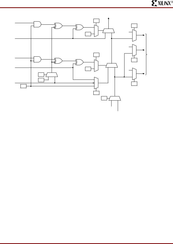
Fast Carry Logic
Each CLB F and G function generator contains dedicated arithmetic logic for the fast generation of carry and borrow signals. This extra output is passed on to the function generator in the adjacent CLB. The carry chain is independent of normal routing resources.
Dedicated fast carry logic greatly increases the efficiency and performance of adders, subtractors, accumulators, comparators and counters. It also opens the door to many new applications involving arithmetic operation, where the previous generations of FPGAs were not fast enough or too inefficient. High-speed address offset calculations in microprocessor or graphics systems, and high-speed addition in digital signal processing are two typical applications.
The two 4-input function generators can be configured as a 2-bit adder with built-in hidden carry that can be expanded to any length. This dedicated carry circuitry is so fast and efficient that conventional speed-up methods like carry generate/propagate are meaningless even at the 16-bit level, and of marginal benefit at the 32-bit level.
This fast carry logic is one of the more significant features of the XC4000 Series, speeding up arithmetic and counting into the 70 MHz range.
The carry chain in XC4000E devices can run either up or down. At the top and bottom of the columns where there are no CLBs above or below, the carry is propagated to the right. (See Figure 11.) In order to improve speed in the high-capacity XC4000X devices, which can potentially have very long carry chains, the carry chain travels upward only, as shown in Figure 12. Additionally, standard interconnect can be used to route a carry signal in the downward direction.
Figure 13 on page 19 shows an XC4000E CLB with dedicated fast carry logic. The carry logic in the XC4000X is similar, except that COUT exits at the top only, and the signal CINDOWN does not exist. As shown in Figure 13, the carry logic shares operand and control inputs with the function generators. The carry outputs connect to the function generators, where they are combined with the operands to form the sums.
Figure 14 on page 20 shows the details of the carry logic for the XC4000E. This diagram shows the contents of the box labeled “CARRY LOGIC” in Figure 13. The XC4000X carry logic is very similar, but a multiplexer on the pass-through carry chain has been eliminated to reduce delay. Additionally, in the XC4000X the multiplexer on the G4 path has a memory-programmable 0 input, which permits G4 to directly connect to COUT. G4 thus becomes an additional high-speed initialization path for carry-in.
The dedicated carry logic is discussed in detail in Xilinx document XAPP 013: “Using the Dedicated Carry Logic in
XC4000.” This discussion also applies to XC4000E devices, and to XC4000X devices when the minor logic changes are taken into account.
The fast carry logic can be accessed by placing special library symbols, or by using Xilinx Relationally Placed Macros (RPMs) that already include these symbols.
CLB  CLB
CLB 
 CLB
CLB  CLB
CLB
|
CLB |
|
|
CLB |
|
|
CLB |
|
|
CLB |
||||
|
|
|
|
|
|
|
|
|
|
|
|
|
|
|
|
|
|
|
|
|
|
|
|
|
|
|
|
|
|
|
|
|
|
|
|
|
|
|
|
|
|
|
|
|
|
|
|
|
|
|
|
|
|
|
|
|
|
|
|
CLB |
|
CLB |
|
CLB |
|
CLB |
|
|
|
|
|
|
|
CLB  CLB
CLB 
 CLB
CLB  CLB
CLB
X6687
Figure 11: Available XC4000E Carry Propagation
Paths
CLB  CLB
CLB  CLB
CLB  CLB
CLB
CLB  CLB
CLB  CLB
CLB  CLB
CLB
CLB  CLB
CLB  CLB
CLB  CLB
CLB
CLB |
CLB |
CLB |
CLB |
X6610
Figure 12: Available XC4000X Carry Propagation Paths (dotted lines use general interconnect)
6-18 |
May 14, 1999 (Version 1.6) |
R
XC4000E and XC4000X Series Field Programmable Gate Arrays
CARRY |
C OUT C IN DOWN |
D IN |
LOGIC |
|
|
|
|
G |
|
|
|
|
|
H |
|
|
Y |
G |
|
|
|
|
|
CARRY |
|
|
|
|
|
G4 |
|
|
|
|
|
G3 |
|
|
|
|
|
|
|
G |
|
|
|
G2 |
|
DIN |
|
|
|
|
|
H |
|
S/R |
|
|
|
G |
D |
Q |
YQ |
|
|
F |
|
|
|
G1 |
|
|
|
|
|
|
|
|
|
EC |
|
COUT0 |
|
|
|
|
|
|
|
H |
|
|
6 |
H1 |
|
|
|
|
|
|
|
DIN |
|
|
|
F |
|
H |
|
S/R |
|
CARRY |
|
G |
D |
Q |
XQ |
|
|
F |
|
|
|
F4 |
|
|
|
EC |
|
|
|
|
|
|
|
F3 |
|
F |
|
|
|
|
|
|
|
|
|
F2 |
|
|
|
|
|
F1 |
|
H |
|
|
|
|
|
|
|
|
|
|
|
|
|
|
X |
|
|
F |
|
|
|
CINUP |
C OUT |
K |
S/R |
EC |
|
|
|
|
|
|
X6699 |
Figure 13: Fast Carry Logic in XC4000E CLB (shaded area not present in XC4000X)
May 14, 1999 (Version 1.6) |
6-19 |
R
XC4000E and XC4000X Series Field Programmable Gate Arrays
|
|
|
|
COUT |
|
G1 |
|
|
M |
|
|
|
|
|
|
|
|
|
|
|
1 |
|
M |
|
|
|
|
|
|
|
|
|
0 |
1 |
G2 |
|
|
I |
0 |
|
|
G4 |
|
|
|
|
|
|
|
|
|
|
G3 |
|
|
|
|
|
C OUT0 |
|
|
|
|
|
TO |
|
|
|
M |
|
FUNCTION |
|
|
|
|
GENERATORS |
|
F2 |
|
|
|
|
|
|
|
|
|
M |
|
|
|
|
1 |
|
|
|
|
|
|
|
|
F1 |
|
|
|
0 |
1 |
|
M |
0 |
|
|
|
|
|
|
F4 |
||
|
|
|
|
|
|
M |
0 |
1 |
|
|
|
M |
|
|
3 |
|
|
F3 |
|
|
1 |
|
M |
|
|
|
|
|
|
M |
|
|
0 |
|
|
|
|
|
M |
|
|
|
|
|
M |
1 |
0 |
X2000 |
|
|
|
C IN UP |
|
|
|
|
|
|
|
|
|
|
|
|
C IN DOWN |
Figure 14: Detail of XC4000E Dedicated Carry Logic
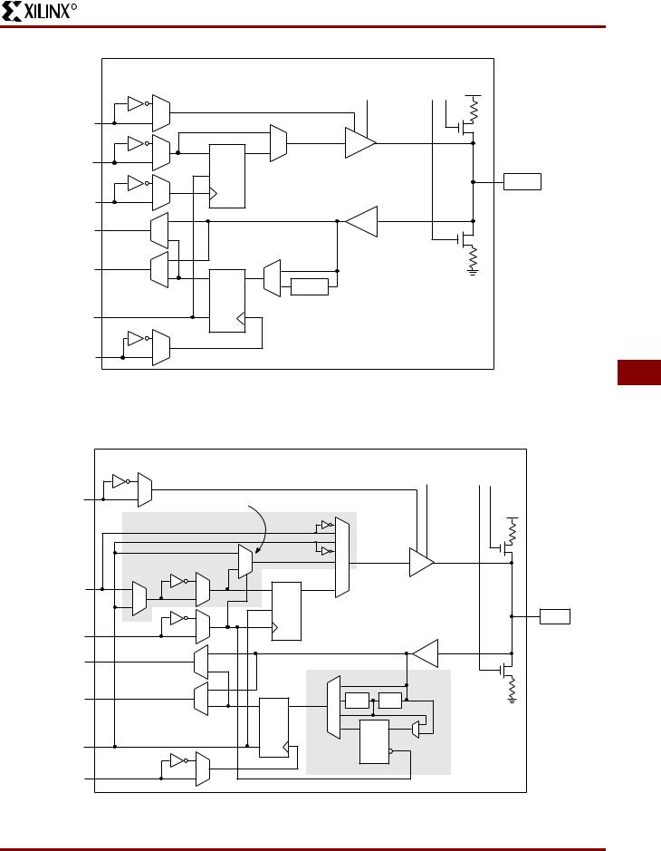
Input/Output Blocks (IOBs)
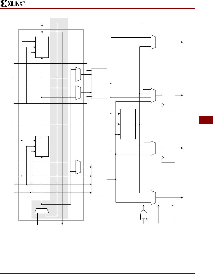
User-configurable input/output blocks (IOBs) provide the interface between external package pins and the internal logic. Each IOB controls one package pin and can be configured for input, output, or bidirectional signals.
Figure 15 shows a simplified block diagram of the XC4000E IOB. A more complete diagram which includes the boundary scan logic of the XC4000E IOB can be found in Figure 40 on page 43, in the “Boundary Scan” section.
The XC4000X IOB contains some special features not included in the XC4000E IOB. These features are highlighted in a simplified block diagram found in Figure 16, and discussed throughout this section. When XC4000X special features are discussed, they are clearly identified in the text. Any feature not so identified is present in both XC4000E and XC4000X devices.
IOB Input Signals
Two paths, labeled I1 and I2 in Figure 15 and Figure 16, bring input signals into the array. Inputs also connect to an input register that can be programmed as either an edge-triggered flip-flop or a level-sensitive latch.
The choice is made by placing the appropriate library symbol. For example, IFD is the basic input flip-flop (rising edge triggered), and ILD is the basic input latch (transpar- ent-High). Variations with inverted clocks are available, and some combinations of latches and flip-flops can be implemented in a single IOB, as described in the XACT Libraries Guide.
The XC4000E inputs can be globally configured for either TTL (1.2V) or 5.0 volt CMOS thresholds, using an option in the bitstream generation software. There is a slight input hysteresis of about 300mV. The XC4000E output levels are also configurable; the two global adjustments of input threshold and output level are independent.
Inputs on the XC4000XL are TTL compatible and 3.3V CMOS compatible. Outputs on the XC4000XL are pulled to the 3.3V positive supply.
The inputs of XC4000 Series 5-Volt devices can be driven by the outputs of any 3.3-Volt device, if the 5-Volt inputs are in TTL mode.
Supported sources for XC4000 Series device inputs are shown in Table 8.
6-20 |
May 14, 1999 (Version 1.6) |
R
XC4000E and XC4000X Series Field Programmable Gate Arrays
Slew Rate |
|
Passive |
|
Pull-Up/ |
|
Control |
|
|
|
Pull-Down |
|
|
|
T |
|
|
|
|
Flip-Flop |
|
|
Out |
D |
Q |
|
|
|
Output |
|
|
CE |
|
Buffer |
|
|
|
Pad |
Output |
|
|
|
Clock |
|
|
|
I1 |
|
|
|
|
Flip- |
Input |
|
|
Flop/ |
Buffer |
|
I2 |
Latch |
|
|
Q |
D |
|
|
|
Delay |
||
|
|
|
|
Clock |
CE |
|
|
Enable |
|
|
|
|
|
|
|
Input |
|
|
|
Clock |
|
|
|
6
X6704
Figure 15: Simplified Block Diagram of XC4000E IOB
Slew Rate |
|
Passive |
|
Pull-Up/ |
|
Control |
|
|
|
Pull-Down |
|
|
|
T
Output MUX
|
0 |
|
|
|
|
1 |
|
|
|
|
Flip-Flop |
|
||
Out |
|
D |
Q |
|
|
|
|
|
Output |
|
|
CE |
|
Buffer |
|
|
|
|
Pad |
Output Clock |
|
|
|
Input |
|
|
|
|
Buffer |
I1 |
|
|
|
|
|
Flip-Flop/ |
|
||
I2 |
Latch |
|
|
|
Q |
D |
Delay |
Delay |
|
|
|
|
||
|
|
|
Q |
D |
Clock Enable |
CE |
|
Latch |
|
|
Fast |
G |
||
|
|
|
Capture |
|
|
|
|
|
|
|
|
|
Latch |
|
Input Clock |
|
|
|
|
|
|
|
|
X5984 |
Figure 16: Simplified Block Diagram of XC4000X IOB (shaded areas indicate differences from XC4000E)
May 14, 1999 (Version 1.6) |
6-21 |

R
XC4000E and XC4000X Series Field Programmable Gate Arrays
Table 8: Supported Sources for XC4000 Series Device Inputs
|
|
XC4000E/EX |
XC4000XL |
||
|
|
Series Inputs |
Series Inputs |
||
Source |
|
|
|
|
|
|
5 V, |
5 V, |
3.3 V |
||
|
|
TTL |
CMOS |
CMOS |
|
|
|
|
|
||
Any device, Vcc = 3.3 V, |
Ö |
|
Ö |
||
CMOS outputs |
|
|
|||
|
|
Unreli |
|
||
|
|
|
|
||
XC4000 Series, Vcc = 5 V, |
Ö |
Ö |
|||
-able |
|||||
TTL outputs |
|
||||
|
|
Data |
|
||
|
|
|
|
||
Any device, Vcc = 5 V, |
Ö |
Ö |
|||
|
|||||
TTL outputs (Voh £ |
3.7 V) |
|
|||
|
|
|
|||
|
|
|
|
||
Any device, Vcc = 5 V, |
Ö |
Ö |
Ö |
||
CMOS outputs |
|
||||
|
|
|
|
||
|
|
|
|
||
XC4000XL 5-Volt Tolerant I/Os |
|
|
|||
The I/Os on the XC4000XL are fully 5-volt tolerant even though the VCC is 3.3 volts. This allows 5 V signals to directly connect to the XC4000XL inputs without damage, as shown in Table 8. In addition, the 3.3 volt VCC can be applied before or after 5 volt signals are applied to the I/Os. This makes the XC4000XL immune to power supply sequencing problems.
Registered Inputs
The I1 and I2 signals that exit the block can each carry either the direct or registered input signal.
The input and output storage elements in each IOB have a common clock enable input, which, through configuration, can be activated individually for the input or output flip-flop, or both. This clock enable operates exactly like the EC pin on the XC4000 Series CLB. It cannot be inverted within the IOB.
The storage element behavior is shown in Table 9.
Table 9: Input Register Functionality (active rising edge is shown)
Mode |
Clock |
Clock |
D |
Q |
|||||
Enable |
|||||||||
|
|
|
|
|
|
|
|
||
|
|
|
|
|
|||||
Power-Up or |
X |
X |
X |
SR |
|||||
GSR |
|
|
|
|
|
|
|||
|
|
|
|
|
|
|
|||
Flip-Flop |
__/ |
|
|
1* |
D |
D |
|||
|
|
||||||||
|
|
|
|
|
|
|
|
|
|
|
|
|
0 |
|
|
X |
X |
Q |
|
|
|
|
|
|
|
|
|||
Latch |
1 |
|
|
1* |
X |
Q |
|||
|
|
|
|
|
|
|
|
|
|
|
|
|
0 |
|
|
1* |
D |
D |
|
|
|
|
|
|
|||||
Both |
X |
0 |
X |
Q |
|||||
|
|
|
|
|
|
|
|||
Legend: |
|
|
|
|
|
|
|||
X |
Don’t care |
|
|
|
|||||
__/ |
|
|
Rising edge |
|
|
|
|||
SR |
Set or Reset value. Reset is default. |
|
|||||||
0* |
|
|
Input is Low or unconnected (default value) |
||||||
1* |
|
|
Input is High or unconnected (default value) |
||||||
Optional Delay Guarantees Zero Hold Time
The data input to the register can optionally be delayed by several nanoseconds. With the delay enabled, the setup time of the input flip-flop is increased so that normal clock routing does not result in a positive hold-time requirement. A positive hold time requirement can lead to unreliable, temperatureor processing-dependent operation.
The input flip-flop setup time is defined between the data measured at the device I/O pin and the clock input at the IOB (not at the clock pin). Any routing delay from the device clock pin to the clock input of the IOB must, therefore, be subtracted from this setup time to arrive at the real setup time requirement relative to the device pins. A short specified setup time might, therefore, result in a negative setup time at the device pins, i.e., a positive hold-time requirement.
When a delay is inserted on the data line, more clock delay can be tolerated without causing a positive hold-time requirement. Sufficient delay eliminates the possibility of a data hold-time requirement at the external pin. The maximum delay is therefore inserted as the default.
The XC4000E IOB has a one-tap delay element: either the delay is inserted (default), or it is not. The delay guarantees a zero hold time with respect to clocks routed through any of the XC4000E global clock buffers. (See “Global Nets and Buffers (XC4000E only)” on page 35 for a description of the global clock buffers in the XC4000E.) For a shorter input register setup time, with non-zero hold, attach a NODELAY attribute or property to the flip-flop.
The XC4000X IOB has a two-tap delay element, with choices of a full delay, a partial delay, or no delay. The attributes or properties used to select the desired delay are shown in Table 10. The choices are no added attribute, MEDDELAY, and NODELAY. The default setting, with no added attribute, ensures no hold time with respect to any of the XC4000X clock buffers, including the Global Low-Skew buffers. MEDDELAY ensures no hold time with respect to the Global Early buffers. Inputs with NODELAY may have a positive hold time with respect to all clock buffers. For a description of each of these buffers, see “Global Nets and Buffers (XC4000X only)” on page 37.
Table 10: XC4000X IOB Input Delay Element
Value |
When to Use |
|
|
full delay |
Zero Hold with respect to Global |
(default, no |
Low-Skew Buffer, Global Early Buffer |
attribute added) |
|
|
|
MEDDELAY |
Zero Hold with respect to Global Early |
|
Buffer |
|
|
NODELAY |
Short Setup, positive Hold time |
|
|
6-22 |
May 14, 1999 (Version 1.6) |
R
XC4000E and XC4000X Series Field Programmable Gate Arrays
Additional Input Latch for Fast Capture (XC4000X only)
The XC4000X IOB has an additional optional latch on the input. This latch, as shown in Figure 16, is clocked by the output clock — the clock used for the output flip-flop — rather than the input clock. Therefore, two different clocks can be used to clock the two input storage elements. This additional latch allows the very fast capture of input data, which is then synchronized to the internal clock by the IOB flip-flop or latch.
To use this Fast Capture technique, drive the output clock pin (the Fast Capture latching signal) from the output of one of the Global Early buffers supplied in the XC4000X. The second storage element should be clocked by a Global Low-Skew buffer, to synchronize the incoming data to the internal logic. (See Figure 17.) These special buffers are described in “Global Nets and Buffers (XC4000X only)” on page 37.
The Fast Capture latch (FCL) is designed primarily for use with a Global Early buffer. For Fast Capture, a single clock signal is routed through both a Global Early buffer and a Global Low-Skew buffer. (The two buffers share an input pad.) The Fast Capture latch is clocked by the Global Early buffer, and the standard IOB flip-flop or latch is clocked by the Global Low-Skew buffer. This mode is the safest way to use the Fast Capture latch, because the clock buffers on both storage elements are driven by the same pad. There is no external skew between clock pads to create potential problems.
To place the Fast Capture latch in a design, use one of the special library symbols, ILFFX or ILFLX. ILFFX is a trans- parent-Low Fast Capture latch followed by an active-High input flip-flop. ILFLX is a transparent-Low Fast Capture latch followed by a transparent-High input latch. Any of the clock inputs can be inverted before driving the library element, and the inverter is absorbed into the IOB. If a single BUFG output is used to drive both clock inputs, the software automatically runs the clock through both a Global Low-Skew buffer and a Global Early buffer, and clocks the Fast Capture latch appropriately.
Figure 16 on page 21 also shows a two-tap delay on the input. By default, if the Fast Capture latch is used, the Xilinx software assumes a Global Early buffer is driving the clock, and selects MEDDELAY to ensure a zero hold time. Select
|
|
ILFFX |
|
IPAD |
D |
Q |
to internal |
|
|
|
logic |
|
GF |
|
|
|
BUFGE |
|
|
|
CE |
|
|
IPAD |
C |
|
|
|
|
|
|
|
BUFGLS |
|
|
|
|
|
X9013 |
the desired delay based on the discussion in the previous subsection.
IOB Output Signals
Output signals can be optionally inverted within the IOB, and can pass directly to the pad or be stored in an edge-triggered flip-flop. The functionality of this flip-flop is shown in Table 11.
An active-High 3-state signal can be used to place the output buffer in a high-impedance state, implementing 3-state outputs or bidirectional I/O. Under configuration control, the output (OUT) and output 3-state (T) signals can be inverted. The polarity of these signals is independently configured for each IOB.
The 4-mA maximum output current specification of many |
|
FPGAs often forces the user to add external buffers, which |
|
are especially cumbersome on bidirectional I/O lines. The |
|
XC4000E and XC4000EX/XL devices solve many of these |
|
problems by providing a guaranteed output sink current of |
|
12 mA. Two adjacent outputs can be interconnected exter- |
|
nally to sink up to 24 mA. The XC4000E and XC4000EX/XL |
|
FPGAs can thus directly drive buses on a printed circuit |
|
board. |
6 |
By default, the output pull-up structure is configured as a |
|
|
|
TTL-like totem-pole. The High driver is an n-channel pull-up |
|
transistor, pulling to a voltage one transistor threshold |
|
below Vcc. Alternatively, the outputs can be globally config- |
|
ured as CMOS drivers, with p-channel pull-up transistors |
|
pulling to Vcc. This option, applied using the bitstream gen- |
|
eration software, applies to all outputs on the device. It is |
|
not individually programmable. In the XC4000XL, all out- |
|
puts are pulled to the positive supply rail. |
|
Table 11: Output Flip-Flop Functionality (active rising edge is shown)
|
|
|
|
Clock |
|
|
|
Mode |
Clock |
|
Enable |
T |
D |
Q |
|
|
|
|
|
|
|
|
|
Power-Up |
X |
|
X |
0* |
X |
SR |
|
or GSR |
|
|
|
|
|
|
|
|
|
|
|
|
|
|
|
|
X |
|
0 |
0* |
X |
Q |
|
|
|
|
|
|
|
|
|
Flip-Flop |
__/ |
|
|
1* |
0* |
D |
D |
|
|||||||
|
|
|
|
|
|
|
|
|
X |
|
X |
1 |
X |
Z |
|
|
|
|
|
|
|
|
|
|
0 |
|
|
X |
0* |
X |
Q |
|
|
|
|
|
|
|
|
Legend:
X Don’t care __/ Rising edge
SR Set or Reset value. Reset is default.
0* Input is Low or unconnected (default value)
1* Input is High or unconnected (default value) Z 3-state
Figure 17: Examples Using XC4000X FCL
May 14, 1999 (Version 1.6) |
6-23 |
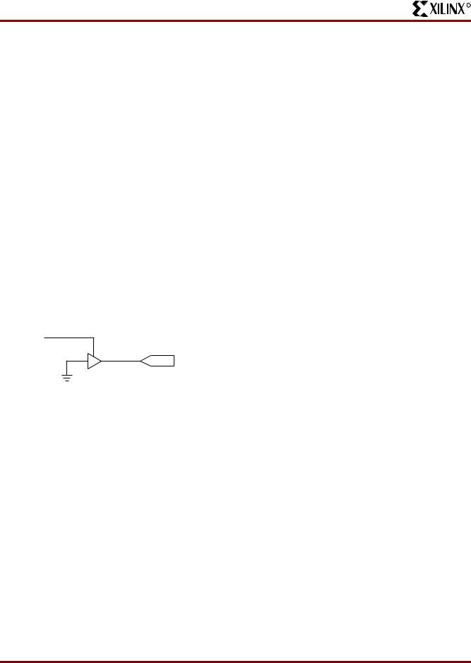
R
XC4000E and XC4000X Series Field Programmable Gate Arrays
Any XC4000 Series 5-Volt device with its outputs configured in TTL mode can drive the inputs of any typical 3.3-Volt device. (For a detailed discussion of how to interface between 5 V and 3.3 V devices, see the 3V Products section of The Programmable Logic Data Book.)
Supported destinations for XC4000 Series device outputs are shown in Table 12.
An output can be configured as open-drain (open-collector) by placing an OBUFT symbol in a schematic or HDL code, then tying the 3-state pin (T) to the output signal, and the input pin (I) to Ground. (See Figure 18.)
Table 12: Supported Destinations for XC4000 Series Outputs
|
XC4000 Series |
|||
|
|
Outputs |
|
|
Destination |
|
|
|
|
3.3 V, |
5 V, |
|
5 V, |
|
|
CMOS |
TTL |
|
CMOS |
|
|
|
|
|
Any typical device, Vcc = 3.3 V, |
Ö |
Ö |
|
some1 |
CMOS-threshold inputs |
|
|
|
|
|
|
|
|
|
Any device, Vcc = 5 V, |
Ö |
Ö |
|
Ö |
TTL-threshold inputs |
|
|
|
|
|
|
|
|
|
Any device, Vcc = 5 V, |
Unreliable |
|
Ö |
|
CMOS-threshold inputs |
Data |
|
|
|
|
|
|
|
|
1. Only if destination device has 5-V tolerant inputs
OPAD
OBUFT
X6702
Figure 18: Open-Drain Output
Output Slew Rate
The slew rate of each output buffer is, by default, reduced, to minimize power bus transients when switching non-criti- cal signals. For critical signals, attach a FAST attribute or property to the output buffer or flip-flop.
For XC4000E devices, maximum total capacitive load for simultaneous fast mode switching in the same direction is 200 pF for all package pins between each Power/Ground pin pair. For XC4000X devices, additional internal
Power/Ground pin pairs are connected to special Power and Ground planes within the packages, to reduce ground bounce. Therefore, the maximum total capacitive load is 300 pF between each external Power/Ground pin pair. Maximum loading may vary for the low-voltage devices.
For slew-rate limited outputs this total is two times larger for each device type: 400 pF for XC4000E devices and 600 pF for XC4000X devices. This maximum capacitive load should not be exceeded, as it can result in ground bounce of greater than 1.5 V amplitude and more than 5 ns duration. This level of ground bounce may cause undesired transient behavior on an output, or in the internal logic. This restriction is common to all high-speed digital ICs, and is not particular to Xilinx or the XC4000 Series.
XC4000 Series devices have a feature called “Soft Start-up,” designed to reduce ground bounce when all outputs are turned on simultaneously at the end of configuration. When the configuration process is finished and the device starts up, the first activation of the outputs is automatically slew-rate limited. Immediately following the initial activation of the I/O, the slew rate of the individual outputs is determined by the individual configuration option for each IOB.
Global Three-State
A separate Global 3-State line (not shown in Figure 15 or Figure 16) forces all FPGA outputs to the high-impedance state, unless boundary scan is enabled and is executing an EXTEST instruction. This global net (GTS) does not compete with other routing resources; it uses a dedicated distribution network.
GTS can be driven from any user-programmable pin as a global 3-state input. To use this global net, place an input pad and input buffer in the schematic or HDL code, driving the GTS pin of the STARTUP symbol. A specific pin location can be assigned to this input using a LOC attribute or property, just as with any other user-programmable pad. An inverter can optionally be inserted after the input buffer to invert the sense of the Global 3-State signal. Using GTS is similar to GSR. See Figure 2 on page 11 for details.
Alternatively, GTS can be driven from any internal node.
6-24 |
May 14, 1999 (Version 1.6) |
R
XC4000E and XC4000X Series Field Programmable Gate Arrays
Output Multiplexer/2-Input Function Generator (XC4000X only)
As shown in Figure 16 on page 21, the output path in the XC4000X IOB contains an additional multiplexer not available in the XC4000E IOB. The multiplexer can also be configured as a 2-input function generator, implementing a pass-gate, AND-gate, OR-gate, or XOR-gate, with 0, 1, or 2 inverted inputs. The logic used to implement these functions is shown in the upper gray area of Figure 16.
When configured as a multiplexer, this feature allows two output signals to time-share the same output pad; effectively doubling the number of device outputs without requiring a larger, more expensive package.
When the MUX is configured as a 2-input function generator, logic can be implemented within the IOB itself. Combined with a Global Early buffer, this arrangement allows very high-speed gating of a single signal. For example, a wide decoder can be implemented in CLBs, and its output gated with a Read or Write Strobe Driven by a BUFGE buffer, as shown in Figure 19. The critical-path pin-to-pin delay of this circuit is less than 6 nanoseconds.
As shown in Figure 16, the IOB input pins Out, Output Clock, and Clock Enable have different delays and different flexibilities regarding polarity. Additionally, Output Clock sources are more limited than the other inputs. Therefore, the Xilinx software does not move logic into the IOB function generators unless explicitly directed to do so.
The user can specify that the IOB function generator be used, by placing special library symbols beginning with the letter “O.” For example, a 2-input AND-gate in the IOB function generator is called OAND2. Use the symbol input pin labelled “F” for the signal on the critical path. This signal is placed on the OK pin — the IOB input with the shortest delay to the function generator. Two examples are shown in Figure 20.
IPAD
BUFGE
F
OPAD
from
internal OAND2 FAST logic
X9019
Figure 19: Fast Pin-to-Pin Path in XC4000X
|
|
|
|
OMUX2 |
||
F |
|
|
D0 |
|||
|
|
|
|
|
O |
|
|
|
|
|
|
|
|
|
|
|
D1 |
|
||
OAND2 |
|
|
|
|||
X6598 |
S0 |
|
||||
|
|
|
||||
|
|
|
|
|
|
X6599 |
Figure 20: AND & MUX Symbols in XC4000X IOB
Other IOB Options
There are a number of other programmable options in the XC4000 Series IOB.
Pull-up and Pull-down Resistors
Programmable pull-up and pull-down resistors are useful for tying unused pins to Vcc or Ground to minimize power consumption and reduce noise sensitivity. The configurable pull-up resistor is a p-channel transistor that pulls to Vcc. The configurable pull-down resistor is an n-channel transistor that pulls to Ground.
The value of these resistors is 50 kΩ − 100 kΩ. This high value makes them unsuitable as wired-AND pull-up resistors.
The pull-up resistors for most user-programmable IOBs are active during the configuration process. See Table 22 on page 58 for a list of pins with pull-ups active before and during configuration.
After configuration, voltage levels of unused pads, bonded or un-bonded, must be valid logic levels, to reduce noise sensitivity and avoid excess current. Therefore, by default,
unused pads are configured with the internal pull-up resis- 6 tor active. Alternatively, they can be individually configured
with the pull-down resistor, or as a driven output, or to be driven by an external source. To activate the internal pull-up, attach the PULLUP library component to the net attached to the pad. To activate the internal pull-down, attach the PULLDOWN library component to the net attached to the pad.
Independent Clocks
Separate clock signals are provided for the input and output flip-flops. The clock can be independently inverted for each flip-flop within the IOB, generating either falling-edge or ris- ing-edge triggered flip-flops. The clock inputs for each IOB are independent, except that in the XC4000X, the Fast Capture latch shares an IOB input with the output clock pin.
Early Clock for IOBs (XC4000X only)
Special early clocks are available for IOBs. These clocks are sourced by the same sources as the Global Low-Skew buffers, but are separately buffered. They have fewer loads and therefore less delay. The early clock can drive either the IOB output clock or the IOB input clock, or both. The early clock allows fast capture of input data, and fast clock-to-output on output data. The Global Early buffers that drive these clocks are described in “Global Nets and Buffers (XC4000X only)” on page 37.
Global Set/Reset
As with the CLB registers, the Global Set/Reset signal (GSR) can be used to set or clear the input and output registers, depending on the value of the INIT attribute or property. The two flip-flops can be individually configured to set
May 14, 1999 (Version 1.6) |
6-25 |
 Loading...