

Page 1

CAN FD v2.0
LogiCORE IP Product Guide
Vivado Design Suite
PG223 December 5, 2018
Page 2

Table of Contents
Send Feedback
IP Facts
Chapter 1: Overview
Core Description. . . . . . . . . . . . . . . . . . . . . . . . . . . . . . . . . . . . . . . . . . . . . . . . . . . . . . . . . . . . . . . . . . . 7
Licensing and Ordering . . . . . . . . . . . . . . . . . . . . . . . . . . . . . . . . . . . . . . . . . . . . . . . . . . . . . . . . . . . . . 8
Chapter 2: Product Specification
Standards . . . . . . . . . . . . . . . . . . . . . . . . . . . . . . . . . . . . . . . . . . . . . . . . . . . . . . . . . . . . . . . . . . . . . . . . 9
Performance. . . . . . . . . . . . . . . . . . . . . . . . . . . . . . . . . . . . . . . . . . . . . . . . . . . . . . . . . . . . . . . . . . . . . . 9
Resource Utilization. . . . . . . . . . . . . . . . . . . . . . . . . . . . . . . . . . . . . . . . . . . . . . . . . . . . . . . . . . . . . . . . 9
Port Descriptions . . . . . . . . . . . . . . . . . . . . . . . . . . . . . . . . . . . . . . . . . . . . . . . . . . . . . . . . . . . . . . . . . . 9
Register Space . . . . . . . . . . . . . . . . . . . . . . . . . . . . . . . . . . . . . . . . . . . . . . . . . . . . . . . . . . . . . . . . . . . 10
Chapter 3: Designing with the Core
Operating Modes and States. . . . . . . . . . . . . . . . . . . . . . . . . . . . . . . . . . . . . . . . . . . . . . . . . . . . . . . . 63
Programming Model . . . . . . . . . . . . . . . . . . . . . . . . . . . . . . . . . . . . . . . . . . . . . . . . . . . . . . . . . . . . . . 68
Clocking. . . . . . . . . . . . . . . . . . . . . . . . . . . . . . . . . . . . . . . . . . . . . . . . . . . . . . . . . . . . . . . . . . . . . . . . . 77
Resets . . . . . . . . . . . . . . . . . . . . . . . . . . . . . . . . . . . . . . . . . . . . . . . . . . . . . . . . . . . . . . . . . . . . . . . . . . 77
Interrupts . . . . . . . . . . . . . . . . . . . . . . . . . . . . . . . . . . . . . . . . . . . . . . . . . . . . . . . . . . . . . . . . . . . . . . . 78
CAN FD v2.0 2
PG223 December 5, 2018 www.xilinx.com
Chapter 4: Design Flow Steps
Customizing and Generating the Core . . . . . . . . . . . . . . . . . . . . . . . . . . . . . . . . . . . . . . . . . . . . . . . . 80
Constraining the Core . . . . . . . . . . . . . . . . . . . . . . . . . . . . . . . . . . . . . . . . . . . . . . . . . . . . . . . . . . . . . 83
Simulation . . . . . . . . . . . . . . . . . . . . . . . . . . . . . . . . . . . . . . . . . . . . . . . . . . . . . . . . . . . . . . . . . . . . . . 84
Synthesis and Implementation . . . . . . . . . . . . . . . . . . . . . . . . . . . . . . . . . . . . . . . . . . . . . . . . . . . . . . 84
Chapter 5: Example Design
Overview . . . . . . . . . . . . . . . . . . . . . . . . . . . . . . . . . . . . . . . . . . . . . . . . . . . . . . . . . . . . . . . . . . . . . . . 85
Simulating the Example Design. . . . . . . . . . . . . . . . . . . . . . . . . . . . . . . . . . . . . . . . . . . . . . . . . . . . . . 86
Page 3

Chapter 6: Test Bench
Send Feedback
Appendix A: Verification, Compliance, and Interoperability
Compliance Testing . . . . . . . . . . . . . . . . . . . . . . . . . . . . . . . . . . . . . . . . . . . . . . . . . . . . . . . . . . . . . . . 89
Appendix B: Upgrading
Upgrading in the Vivado Design Suite . . . . . . . . . . . . . . . . . . . . . . . . . . . . . . . . . . . . . . . . . . . . . . . . 90
Appendix C: Debugging
Finding Help on Xilinx.com . . . . . . . . . . . . . . . . . . . . . . . . . . . . . . . . . . . . . . . . . . . . . . . . . . . . . . . . . 91
Debug Tools . . . . . . . . . . . . . . . . . . . . . . . . . . . . . . . . . . . . . . . . . . . . . . . . . . . . . . . . . . . . . . . . . . . . . 93
Hardware Debug . . . . . . . . . . . . . . . . . . . . . . . . . . . . . . . . . . . . . . . . . . . . . . . . . . . . . . . . . . . . . . . . . 93
Interface Debug . . . . . . . . . . . . . . . . . . . . . . . . . . . . . . . . . . . . . . . . . . . . . . . . . . . . . . . . . . . . . . . . . . 94
Appendix D: Additional Resources and Legal Notices
Xilinx Resources . . . . . . . . . . . . . . . . . . . . . . . . . . . . . . . . . . . . . . . . . . . . . . . . . . . . . . . . . . . . . . . . . . 96
Documentation Navigator and Design Hubs . . . . . . . . . . . . . . . . . . . . . . . . . . . . . . . . . . . . . . . . . . . 96
References . . . . . . . . . . . . . . . . . . . . . . . . . . . . . . . . . . . . . . . . . . . . . . . . . . . . . . . . . . . . . . . . . . . . . . 97
Revision History . . . . . . . . . . . . . . . . . . . . . . . . . . . . . . . . . . . . . . . . . . . . . . . . . . . . . . . . . . . . . . . . . . 98
Please Read: Important Legal Notices . . . . . . . . . . . . . . . . . . . . . . . . . . . . . . . . . . . . . . . . . . . . . . . . 98
CAN FD v2.0 3
PG223 December 5, 2018 www.xilinx.com
Page 4

IP Facts
Send Feedback
Introduction
The Xilinx® LogiCORE™ IP CAN with Flexible
Data Rate (CAN FD) core is ideally suited for
automotive and industrial applications such as
automotive body control units, automotive test
equipment, instrument clusters, sensor
controls, and industrial networks. The core can
be used in standalone mode or connected to
Xilinx MicroBlaze™ processors or the Arm
Cortex-A9 processors in Zynq
®
-7000 SoCs.
®
Features
• Designed to ISO 11898-1/2015
specification [Ref 1]
• Supports both CAN and CAN FD frames
• Supports the CAN FD frame format
specified in the ISO 11898:2015
specification [Ref 1]
• Supports up to 64 byte CAN FD frames
• Supports flexible data rates up to 8 Mb/s
• Supports nominal data rates up to 1Mb/s
• Up to three data bit transmitter delay
compensation
• TX and RX mailbox buffers with
configurable depth
• Two 64-deep RX FIFOs with 32 ID
Filter-Mask pairs
• Message with lowest ID transmitted first
• Supports TX message cancellation
IMPORTANT: It is required to have a valid Bosch CAN
FD protocol license before selling a device containing
the Xilinx CAN FD IP core.
LogiCORE™ IP Facts Table
Core Specifics
UltraScale+™
Supported
Device Family
Supported User
Interfaces
Resources Performance and Resource Utilization web page
(1)
Zynq UltraScale+ MPSoC Architecture
Zynq
®
UltraScale™
-7000 SoC, 7 Series,
AXI4-Lite, APB
Provided with Core
Design Files Encrypted RTL
Example Design Verilog
Test Bench Verilog
Constraints File XDC
Simulation
Model
Supported
S/W Driver
(2)
Tested Design Flows
Design Entry Vivado® Design Suite
Simulation
Synthesis Vivado Synthesis
For supported simulators, see the
Xilinx Design Tools: Release Notes Guide.
Not Provided
Standalone and Linux
(3)
Support
Provided by Xilinx at the Xilinx Support web page
Notes:
1. For a complete listing of supported devices, see the Vivado IP
catalog
.
2. Standalone driver details can be found in the SDK directory
(\Xilinx\SDK\<release_version>\data\embeddedsw\XilinxPro
cessorIPLib\drivers\canfd_version). Linux OS and driver
support information is available from the Linux CAN FD
Driver Page.
3. For the supported versions of the tools, see the
Xilinx Design Tools: Release Notes Guide.
• Separate error logging for fast data rate
CAN FD v2.0 4
PG223 December 5, 2018 www.xilinx.com Product Specification
Page 5

Other Features
Send Feedback
• Timestamp for transmitted and received messages
• Supports transmit event FIFO
• Supports the following modes:
Disable Auto-Retransmission (DAR) mode
°
Snoop (Bus Monitoring) mode
°
Sleep mode with Wake-Up Interrupt
°
Internal Loopback mode
°
Bus-Off Recovery mode
°
-Auto-Recovery
- User intervention for Auto-Recovery
Disable Protocol Exception Event mode
°
IP Facts
CAN FD v2.0 5
PG223 December 5, 2018 www.xilinx.com
Page 6

Overview
CAN FD Core
Host
Control
Object Layer/LLC
AXI4-Lite
I/F
TX Block
RAM
TBMM
Register Module
RX Block
RAM
RBMM
CDC
Sync
AXI Clock Domain
CAN FD Protocol Engine
Transfer Layer/MAC
CAN Clock Domain
PHY
CAN Bus
TX
RX
AXI4-Lite Bus
X14811-081418
Send Feedback
This product guide describes features of the CAN FD core and the functionality of the
various registers in the design. In addition, the core interface and its customization options
are defined in this document. Information on the CAN or CAN FD protocol is outside the
scope of this document, and knowledge of the relevant CAN and CAN FD specifications is
assumed. Figure 1-1 illustrates the high-level architecture of the CAN FD core and provides
the interface connectivity.
X-Ref Target - Figure 1-1
Chapter 1
CAN FD v2.0 6
PG223 December 5, 2018 www.xilinx.com
Note:
Figure 1-1: CAN FD Core Layered Architecture and Connectivity
The core requires an external PHY to be connected to communicate on the CAN bus.
Page 7

Chapter 1: Overview
Send Feedback
Core Description
The core functions are divided into two independent layers as shown in Figure 1-1. The
object layer interfaces with the host control through the AXI4-Lite/APB interface and works
in the AXI4-Lite/APB clock domain. The transfer layer interfaces with the external PHY and
operates in the CAN clock domain. Information exchange between the two layers is done
through the CDC synchronizers. The CAN FD object layer provides a state-of-the-art
transmission and reception method to manage message buffers.
Object Layer (Logical Link Layer)
The object layer is divided into the following submodules:
• Register Module – This module allows for read and write access to the registers
through the external host interface.
• TX Buffer Management Module – The TX Buffer Management Module (TBMM)
interfaces with the CAN FD protocol engine to provide the next buffer to transmit on
the CAN bus. It manages the host access to the TX block RAM.
• RX Buffer Management Module – The RX Buffer Management Module (RBMM)
interfaces with the CAN FD protocol engine to provide storage for message reception
from the CAN bus. It manages the host access to the RX block RAM.
Transfer Layer (Medium Access Control Layer)
The transfer layer provides the following main functions:
• Initiation of the transmission process after recognizing bus idle (compliance with
inter-frame space)
Serialization of the frame
°
Bit stuffing
°
Arbitration and passing into receive mode in case of loss of arbitration
°
ACK check
°
Presentation of a serial bitstream to PHY for transmission
°
CRC sequence calculation including stuff bit count for FD frames
°
Bit rate switching
°
CAN FD v2.0 7
PG223 December 5, 2018 www.xilinx.com
• Reception of a serial bitstream from the PHY
Deserialization and recompiling of the frame structure
°
Bit destuffing
°
Page 8

Chapter 1: Overview
Send Feedback
Transmission of ACK
°
Bit rate switching
°
• Bit timing functions
• Error detection and signaling
• Recognition of an overload condition and reaction
Licensing and Ordering
IMPORTANT: It is required to have a valid Bosch CAN FD protocol license before selling a device
containing the Xilinx CAN FD IP core.
License Checkers
If the IP requires a license key, the key must be verified. The Vivado® design tools have
several license checkpoints for gating licensed IP through the flow. If the license check
succeeds, the IP can continue generation. Otherwise, generation halts with error. License
checkpoints are enforced by the following tools:
• Vivado synthesis
• Vivado implementation
• write_bitstream (Tcl command)
IMPORTANT: IP license level is ignored at checkpoints. The test confirms a valid license exists. It does
not check IP license level.
License Type
The core is provided under the terms of the CAN FD LogiCORE™ IP License Agreement for
Automotive or Non-Automotive applications. Click here for more information about
obtaining a CAN FD license.
For more information, visit the CAN FD product web page.
Information about other Xilinx LogiCORE IP modules is available at the Xilinx Intellectual
Property page. For information on pricing and availability of other Xilinx LogiCORE IP
modules and tools, contact your local Xilinx sales representative.
CAN FD v2.0 8
PG223 December 5, 2018 www.xilinx.com
Page 9

Product Specification
Send Feedback
Standards
The CAN FD core conforms to the ISO-11898-1/2015 standard specification [Ref 1].
Performance
For full details about performance, visit the Performance and Resource Utilization web
page.
Chapter 2
Resource Utilization
For full details about resource utilization, visit the Performance and Resource Utilization
web page.
Port Descriptions
The host interface of the CAN FD core is either the AXI4-Lite or the APB interface,
depending on the parameter selected in the Vivado™ IDE. Ta bl e 2-1 defines the core
interface signaling.
Table 2-1: CAN FD Core I/O Signals
Signal Name Interface Type Default Description
AXI4-Lite Interface Signals
(1)
s_axi_*
ip2bus_intrevent Interrupt O 0x0 Active-High interrupt line.
S_AXI_LITE – –
Clock, Interrupt, and PHY Signals
See the Vivado AXI Reference Guide (UG1037)
[Ref 7] for the description of the AXI4 signals.
(2)(3)
CAN FD v2.0 9
PG223 December 5, 2018 www.xilinx.com
Page 10

Chapter 2: Product Specification
Send Feedback
Table 2-1: CAN FD Core I/O Signals
Signal Name Interface Type Default Description
can_clk Clock
can_phy_tx PHY O 1 CAN bus transmit signal to PHY.
can_phy_rx PHY I – CAN bus receive signal from PHY.
can_clk_x2 Clock I - This is fully synchronous to the CAN clock and is
I–
CAN clock input. Oscillator frequency tolerance
according to the standard specification.
a multiple by 2 in frequency.
APB Interface Signals
apb_clk Clock I - APB clock.
apb_resetn Reset I - Active-Low synchronous reset.
apb_pwdata[31:0] APB I - Write data bus.
apb_paddr[14:0] I - Address bus.
apb_pwrite I - Read or Write signaling:
• 0 for Read Transaction.
• 1 for Write Transaction.
apb_psel I - Active-High select.
apb_penable I - Active-High enable.
apb_prdata[31:0] O 0x0 Read Data bus.
apb_pready O 0x0 Active-High ready signal.
apb_perror APB O 0x0 Active-High R/W er ro r s ignal. Re served fo r f ut ure
use.
Notes:
1. The core does not support the wstrb signal on the AXI4-Lite interface.
2. The interrupt line is level-sensitive. Interrupts are indicated by the transition of the interrupt line logic from 0 to 1.
3. The AXI4-Lite interface signals and ip2bus_intrevent are synchronous to the s_axi_aclk clock.
Register Space
The CAN FD core requires a 32 KB memory mapped space to be allocated in the system
memory. Division of this addressable space within the core is shown in Tab le 2 -2.
Note:
and is not impacted by the AXI Write Data Strobe (*_wstrb) signal. For write access, both the AXI
Write Address Valid (*_awvalid) and AXI Write Data Valid (*_wvalid) signals should be asserted
together.
The AXI4-Lite write access register is updated by the 32-bit AXI Write Data (*_wdata) signal,
CAN FD v2.0 10
PG223 December 5, 2018 www.xilinx.com
Page 11

Chapter 2: Product Specification
Send Feedback
Table 2-2: CAN FD Address Space Division
Start Address End Address Section Notes
0x0000 0x00FF Core Registers Space
0x0100 0x1FFF TX Message Space
0x2000 0x7FFF RX Message Space
This space is implemented with flip-flops. See
Tabl e 2- 3 and Ta ble 2 -4.
This space is implemented with TX block RAM
and provides storage for a maximum 32 TX
buffers. For RX Sequential buffer mode (FIFO
mode), it also
provides storage for 32 ID Filter-Mask pairs. See
Tabl e 2- 30 .
This space is implemented with RX block RAM.
For RX Sequential buffer mode (FIFO mode), it
provides storage for two 64-deep message RX
FIFO's. See Table 2- 37 and Table 2 -38.
It provides storage for 32 deep TX Event FIFO.
See Tabl e 2- 34 .
For RX Ma il box buff er mo de, it provides storage
for maximum 48 RX Buffers and respective ID
Masks. See Ta bl e 2 -44.
Table 2-3: CAN FD Core Register Address Map
Start
Address
0x0000 SRR Read, Write Software Reset Register
Name Access Description Notes
0x0004 MSR Read, Write Mode Select Register
0x0008 BRPR Read, Write
0x000C BTR Read, Write Arbitration Phase Bit Register
0x0010 ECR Read Error Counter Register
0x0014 ESR
0x0018 SR Read Status Register
0x001C ISR Read Interrupt Status Register
0x0020 IER Read, Write Interrupt Enable Register
0x0024 ICR Write Interrupt Clear Register
0x0028 TSR Read, Write Timestamp Register
0x002C0x0084
0x0088 DP_BRPR Read, Write Data Phase Baud Rate Prescaler Register
0x008C DP_BTR Read, Write Data Phase Bit Timing Register
0x0090 TRR Read, Write TX Buffer Ready Request Register
0x0094 IETRS Read, Write
Reserved –
Read, Write
1 to clear
Arbitration Phase Baud Rate Prescaler
Register
Error Status Register
Reserved space. Write has no effect. Read
always returns 0.
Interrupt Enable TX Buffer Ready Request
Served/Cleared Register
Registers present in
both RX Mailbox
and RX Sequential/
FIFO buffer modes.
CAN FD v2.0 11
PG223 December 5, 2018 www.xilinx.com
Page 12

Table 2-3: CAN FD Core Register Address Map (Cont’d)
Send Feedback
Chapter 2: Product Specification
Start
Address
Name Access Description Notes
0x0098 TCR Read, Write TX Buffer Cancel Request Register
0x009C IETCS Read, Write
Interrupt Enable TX Buffer Cancellation
Request Served/Cleared Register
0x00A0 TxE_FSR Read, Write TX Event FIFO Status Register.
0x00A4 TxE_WMR Read, Write TX Event FIFO Watermark Register.
0x00A80x00AC
Reserved –
Reserved space. Write has no effect. Read
always returns 0.
0x00B0 RCS0 Read, Write RX Buffer Control Status Register 0
0x00B4 RCS1 Read, Write
See RX Buffer Control Status Register 0
0x00B8 RCS2 Read, Write
0x00BC Reserved –
Reserved space. Write has no effect. Read
always returns 0.
0x00C0 IERBF0 Read, Write Interrupt Enable RX Buffer Full Register 0
0x00C4 IEBRF1 Read, Write Interrupt Enable RX Buffer Full Register 1
0x00C80x00DC
Reserved –
Reserved space. Write has no effect. Read
always returns 0.
0x00E0 AFR Read, Write Acceptance Filter (Control) Register
Registers present in
both RX Mailbox
and RX Sequential/
FIFO buffer modes.
Registers present
only in RX Mailbox
buffer mode.
Otherwise reserved.
0x00E4 Reserved –
0x00E8 FSR Read, Write RX FIFO Status Register
0x00EC WMR Read, Write RX FIFO Watermark Register
0x00F00x00FF
Reserved –
Core Register Descriptions
Tab le 2 -4 shows the CAN FD core register space. The thick ruling represents the RX Mailbox
specific register bits and the gray represents the RX FIFO specific register bits. Register bits
tha t are us ed in both RX Ma ilbox a nd RX FI FO mode and dif fer in d escription a re show n with
a / separator.
Table 2-4: CAN FD Core Register Space
Start
Address
0x0000
313029282726252423222120191817161514131211109876543210
RSVD
Reserved space. Write has no effect. Read
always returns 0.
Reserved space. Write has no effect. Read
always returns 0.
Registers present
only in RX
Sequential/FIFO
buffer mode
otherwise reserved.
Name
(Reset
Val ue)
SRR (0x0)
CEN
SRST
0x0004
CAN FD v2.0 12
PG223 December 5, 2018 www.xilinx.com
RSVD RSVD
MSR (0x0)
ABR
SBR
DPEE
DAR
BRSD
SNOOP
LBACK
SLEEP
Page 13

Table 2-4: CAN FD Core Register Space (Cont’d)
Send Feedback
Start
Address
0x0008
313029282726252423222120191817161514131211109876543210
RSVD BRP [7:0]
Chapter 2: Product Specification
Name
(Reset
Val ue)
BRPR
(0x0)
0x000C
0x0010
0x0014
0x0018
0x001C
0x0020
RSVD SJW[6:0]
RSVD REC[7:0] TEC[7:0] ECR (0x0)
RSVD
RSVD TDCV[6:0] RSVD
RXBOFLW_I [5:0] RXLRM_BI [5:0]
TXEWMFLL
TXEOFLW
RSVD
RXMNF
TS2[6:0] TS1[7:0] BTR (0x0)
RSVD
F_BERR
F_STER
F_FMER
F_CRCER
RSVD
SNOOP
RSVD
BSFR_CONFIG
PEE_CONFIG
ESTAT [1:0]
RXBOFLW/RXFWMFLL_1
RXBFL/RXFOFLW_1
TXCRS
TXRRS
RXFWMFLL
WKUP
SLP
BSOFF
ERROR
RSVD
ERRWRN
RXFOFLW
ACKER
BERR
STER
FMER
BBSY
BIDLE
NORMAL
SLEEP
LBACK
TSCNT_OFLW
RXOK
BSFRD
PEE
TXOK
ESR (0x0)
CRCER
SR (0x1)
CONFIG
ISR (0x0)
ARBLST
IER (0x0)
0x0024
0x0028
0x002C
0x0084
0x0088
0x008C
0x0090
ETXEWMFLL
ETXEOFLW
RSVD
CTXEWMFLL
CTXEOFLW
TIMESTAMP_CNT[15:0] RSVD
RSVD Reserved
RSVD
RR21
DP_SJW
[3:0]
RR20
RSVD
RR31
RR30
RR29
RR28
RR27
RR26
RR25
RR24
RR23
RR22
RR19
RR18
ERXMNF
CRXMNF
TDC_EN
RR17
ERXBOFLW/ERXFWMFLL_1
CRXBOFLW/CRXFWMFLL_1
RSVD
RR16
ERXBFL/ERXFOFLW_1
ETXCRS
ETXRRS
ERXFWMFLL
EWKUP
ESLP
EBSOFF
CRXBFL/CRXFOFLW_1
CTXCRS
CTXRRS
CRXFWMFLL
CWKUP
CSLP
CBSOFF
TDCOFF [5:0] DP_BRP [7:0]
RSVD
DP_TS2
[3:0]
RR15
RR14
RR13
RR12
RR11
RR10
RR9
EERROR
RSVD
ERXOFLW
ETSCNT_OFLW
ERXOK
CERROR
RSVD
CRXOFLW
CTSCNT_OFLW
CRXOK
RSVD DP_TS1[4:0]
RR8
RR7
RR6
RR5
RR4
EBSFRD
CBSFRD
RR3
EPEE
CPEE
RR2
ETXOK
CTXOK
RR1
EARBLST
ICR (0x0)
CARBLST
TSR (0x0)
CTS
DP_BRPR
(0x0)
DP_BTR
(0x0)
TRR (0x0)
RR0
CAN FD v2.0 13
PG223 December 5, 2018 www.xilinx.com
Page 14

Table 2-4: CAN FD Core Register Space (Cont’d)
Send Feedback
Start
Address
313029282726252423222120191817161514131211109876543210
Chapter 2: Product Specification
Name
(Reset
Val ue)
0x0094
0x0098
0x009C
0x00A0
0x00A4
0x00A8
0x00AC
0x00B0
0x00B4
0x00B8
0x00BC
IETRS
ERRS31
ERRS30
ERRS29
ERRS28
ERRS27
ERRS26
ERRS25
ERRS24
ERRS23
ERRS22
ERRS21
ERRS20
ERRS19
ERRS18
ERRS17
ERRS16
ERRS15
ERRS14
ERRS13
ERRS12
ERRS11
ERRS10
ERRS9
ERRS8
ERRS7
ERRS6
ERRS5
ERRS4
ERRS3
ERRS2
CR31
CR30
CR29
CR28
CR27
CR26
CR25
CR24
CR23
CR22
CR21
CR20
CR19
CR18
CR17
CR16
CR15
CR14
CR13
CR12
CR11
CR10
CR9
CR8
CR7
CR6
CR5
CR4
CR3
CR2
ECRS31
ECRS30
ECRS29
ECRS28
ECRS27
ECRS26
ECRS25
ECRS24
ECRS23
ECRS22
ECRS21
ECRS20
ECRS19
ECRS18
ECRS17
ECRS16
ECRS15
ECRS14
ECRS13
ECRS12
ECRS11
ECRS10
ECRS9
ECRS8
ECRS7
ECRS6
ECRS5
ECRS4
ECRS3
ECRS2
RSVD TXE_FL[5:0]
RSVD TXE_FWM[4:0]
RSVD Reserved
RSVD Reserved
CSB15
CSB14
CSB13
CSB12
CSB11
CSB10
CSB9
CSB8
CSB7
CSB6
CSB5
CSB4
CSB3
CSB2
CSB1
CSB0
HCB15
HCB14
HCB13
HCB12
HCB11
HCB10
CSB31
CSB30
CSB29
CSB28
CSB27
CSB26
CSB25
CSB24
CSB23
CSB22
CSB21
CSB20
CSB19
CSB18
CSB17
CSB16
HCB31
HCB30
HCB29
HCB28
HCB27
HCB26
CSB47
CSB46
CSB45
CSB44
CSB43
CSB42
CSB41
CSB40
CSB39
CSB38
CSB37
CSB36
CSB35
CSB34
CSB33
CSB32
HCB47
HCB46
HCB45
HCB44
HCB43
HCB42
RSVD Reserved
HCB9
HCB8
HCB25
HCB24
HCB41
HCB40
TXE_IRI
HCB7
HCB23
HCB39
RSVD
HCB6
HCB5
HCB22
HCB21
HCB38
HCB37
TXE_RI[4:0]
HCB4
HCB3
HCB20
HCB19
HCB36
HCB35
HCB2
HCB18
HCB34
ERRS1
ERRS0
CR1
CR0
ECRS1
ECRS0
HCB1
HCB0
HCB17
HCB16
HCB33
HCB32
(0x0)
TCR (0x 0)
IETCS
(0x0)
TxE _F SR
(0x0)
TxE _W MR
(0xF)
RCS0
(0x0)
RCS1
(0x0)
RCS2
(0x0)
0x00C0
0x00C4
0x00C8
0x00CC
0x00D0
0x00D4
0x00D8
0x00DC
0x00E0
0x00E4
0x00E8
0x00EC
0x00F0
0x00F4
IERBF
ERBF31
ERBF30
ERBF29
ERBF28
ERBF27
ERBF26
ERBF25
ERBF24
ERBF23
ERBF22
ERBF21
ERBF20
ERBF19
ERBF18
ERBF17
ERBF16
ERBF15
ERBF14
ERBF13
ERBF12
ERBF11
ERBF10
ERBF9
ERBF8
ERBF7
ERBF6
ERBF5
ERBF4
ERBF3
ERBF2
RSVD
ERBF47
ERBF46
ERBF45
ERBF44
ERBF43
ERBF42
ERBF41
ERBF40
ERBF39
ERBF38
ERBF37
ERBF36
ERBF35
ERBF34
RSVD Reserved
RSVD Reserved
RSVD Reserved
RSVD Reserved
RSVD Reserved
RSVD Reserved
UAF31
UAF30
UAF29
UAF28
UAF27
UAF26
UAF25
UAF24
UAF23
UAF22
UAF21
UAF20
UAF19
UAF18
UAF17
UAF16
UAF15
UAF14
UAF13
UAF12
UAF11
UAF10
UAF9
UAF8
UAF7
UAF6
UAF5
UAF4
UAF3
UAF2
RSVD Reserved
(1)
FL_1[6:0]
RSVD
RSVD RXFP[4:0]
RSVD Reserved
RSVD Reserved
(1)
IRI_1
RSVD
RI_1[5:0]
(1)
FL[6:0]
RSVD
RSVD
RXFWM_1[5:0]
RI[5:0] FSR (0x0)
IRI
RSVD
RXFWM[5:0]
RSVD
ERBF1
ERBF33
UAF1
(0x0)
ERBF0
IERBF
(0x0)
ERBF32
AFR (0x0)
UAF0
WMR
(0xF)
CAN FD v2.0 14
PG223 December 5, 2018 www.xilinx.com
Page 15

Chapter 2: Product Specification
Send Feedback
Table 2-4: CAN FD Core Register Space (Cont’d)
Start
Address
0x00F8
0x00FC
Notes:
1. These fields are only available when the IP is configured in FIFO (Sequential) Mode and RX FIFO-1 is enabled.
313029282726252423222120191817161514131211109876543210
RSVD Reserved
RSVD Reserved
Software Reset Register (Address Offset + 0x0000)
Writing to the Software Reset register (SRR) places the core in Configuration mode. In
Configuration mode, the core drives recessive on the bus line and does not transmit or
receive messages. During power-up, the CEN and SRST bits are 0 and the CONFIG bit in the
Status register (SR) is 1. The Transfer Layer Configuration registers can be changed only
when the CEN bit in the SRR is 0. Mode Select register bits (except SLEEP and SBR) can be
changed only when the CEN bit is 0. If the CEN bit is changed during core operation, Xilinx
recommends resetting the core so that operation starts over.
Name
(Reset
Val ue)
Table 2-5: Software Reset Register
Bits Name Access
31:2 Reserved – 0 Reserved.
1CENR/W0
0SRSTWO0
Default
Value
CAN Enable.
This is the Enable bit for the core.
• 1 = The core is in Loopback, Sleep, Snoop, or Normal mode,
depending on the LBACK, SLEEP, and SNOOP bits in the MSR.
• 0 = The core is in Configuration mode.
Note:
If the CEN bit is cleared during core operation, Xilinx recommends
resetting the core so that operation starts over.
Reset.
This is the software reset bit for the core.
• 1 = Core is reset.
If a 1 is written to this bit, all core configuration registers
(including the SRR) are reset. Reads to this bit always return 0.
After performing a soft or hard reset, wait for 16 AXI4-Lite/APB
Note:
clock cycles before initiating next AXI4-Lite/APB transaction.
Mode Select Register (Address Offset + 0x0004)
Description
CAN FD v2.0 15
PG223 December 5, 2018 www.xilinx.com
Writing to the Mode Select register (MSR) enables the core to enter Snoop, Sleep,
Loopback, or Normal modes. In Normal mode, the core participates in normal bus
communication. If the SLEEP bit is set to 1, the core enters Sleep mode. If the LBACK bit is
set to 1, the core enters Loopback mode. If the SNOOP mode is set to 1, the core enters
Snoop mode and does not participate in bus communication but only receives messages.
Page 16

Chapter 2: Product Specification
Send Feedback
IMPORTANT: LBACK, SLEEP, and SNOOP bits should never be set to 1 at the same time. At any given
point, the core can either be in Loopback, Sleep, or Snoop mode. When all three bits are set to 0, the
core can enter Normal mode subject to other conditions.
Table 2-6: Mode Select Register
Bits Name Access
31:16 Reserved – 0 Reserved.
15:8 Reserved – 0 Reserved.
7ABRR/W0
6SBRR/W0
5DPEER/W 0
Default
Value
Auto Bus-Off Recovery Request.
• 1 = Auto Bus-Off Recovery request.
• 0 = No such request.
If this bit is set, the node does auto Bus-Off Recovery
irrespective of the SBR bit setting in this register. This bit can be
written only when the CEN bit in SRR is 0.
Start Bus-Off Recovery Request.
• 1 = Start Bus-Off Recovery request.
• 0 = No such request.
Node stays i n Bus-Of f state until th e SBR bi t is set to 1 (pro viding
that the ABR bit in this register is not set).
This bit can be written only when node is in Bus-Off state.
This bit auto clears after node completes the Bus-Off Recovery
or leaves Bus-Off state due to hard/soft reset or CEN
deassertion.
Disable Protocol Exception Event Detection/Generation.
• 1 = Disable Protocol Exception Event detection/generation by
CAN FD receiver if “res” bit in CAN FD frame is detected as 1.
In this case, CAN FD receiver generates Form error.
• 0 = PEE detection/generation is enabled. If the CAN FD
receiver detects th e res bit as 1, it go es to Bus In teg rat ion state
(PEE_config) and waits for Bus Idle condition (11 consecutive
nominal recessive bits). The error counter remains unchanged.
This bit can be written only when the CEN bit in SRR is 0.
Description
CAN FD v2.0 16
PG223 December 5, 2018 www.xilinx.com
Disable Auto-Retransmission.
• 1 = Disable auto retransmission on the CAN bus to provide
4DARR/W0
• 0 = Auto retransmission enabled.
This bit can be written only when the CEN bit in SRR is 0.
CAN FD Bit Rate Switch Disable Override.
• 1 = Makes the core transmit CAN FD frames only in nominal
3BRSDR/W 0
• 0 = Makes the core transmit CAN FD frames as per BRS bit in
This bit can be written only when the CEN bit in SRR is 0.
single shot transmission.
bit rate (by overriding the TX Message element BRS bit
setting).
the TX Message element.
Page 17

Table 2-6: Mode Select Register (Cont’d)
Send Feedback
Chapter 2: Product Specification
Bits Name Access
2 SNOOP R/W 0
1LBACKR/W 0
Default
Value
Description
SNOOP Mode Select/Request.
This is the Snoop mode request bit.
• 1 = Request core to be in Snoop mode.
• 0 = No such request.
This bit can be written only when CEN bit in SRR is 0.
Make sure that Snoop mode is programmed only after system
reset or software reset. For the core to enter Snoop mode, LBACK
and SLEEP bits in this register should be set to 0. The features of
Snoop mode are as follows:
• The core transmits recessive bits onto the CAN bus.
• The core receives messages that are transmitted by other
node s but do es not AC K. St o res re ceived message s in RX b lock
RAM based on programmed ID filtering.
• Error counters are disabled and cleared to 0. Reads to the error
counter register return zero.
Loopback Mode Select/Request.
This is the Loopback mode request bit.
• 1 = Request core to be in Loopback mode.
• 0 = No such request.
This bit can be written only when the CEN bit in SRR is 0. For the
core to enter Loopback mode, SLEEP and SNOOP bits in this
register should be set to 0.
Sleep Mode Select/Request.
This is the Sleep mode request bit.
• 1 = Request core to be in Sleep mode.
0SLEEPR/W 0
• 0 = No such request.
Th is bit is cleare d when the core wakes up fr om Sleep m ode. Fo r
the core to enter Sleep mode, LBACK and SNOOP bits in this
register should be set to 0.
Arbitration Phase (Nominal) Baud Rate Prescaler Register (Address Offset + 0x0008)
The CAN clock for the core is divided by (programmed prescaler value + 1) to generate the
quantum clock needed for sampling and synchronization.
Table 2-7: Arbitration Phase Baud Rate Prescaler Register
Bits Name Access
31:8 Reserved – 0 Reserved.
7:0 BRP[7:0] R/W 0
Default
Value
Description
Arbitration Phase (Nominal) Baud Rate Prescaler.
These bits indicate the prescaler value.
The a c tual v alue is o ne more than the value w ritten t o the re gister.
These bits can be written only when the CEN bit in SRR is 0.
CAN FD v2.0 17
PG223 December 5, 2018 www.xilinx.com
Page 18

Chapter 2: Product Specification
Send Feedback
Arbitration Phase (Nominal) Bit Timing Register (Address Offset + 0x000C)
Table 2-8: Arbitration Phase Bit Register
Bits Name Access
31:23 Reserved – 0 Reserved.
22:16 SJW[6:0] R/W 0
15 Reserved – 0 Reserved.
14:8 TS2[6:0] R/W 0
7:0 TS1[7:0] R/W 0
Default
Value
Synchronization Jump Width.
Indicates the Synchronization Jump Width as specified in the
standard for Nominal Bit Timing.
The actual value is one more than the value written to the register.
These bits can be written only when the CEN bit in SRR is 0.
Time Segment 2
Indicates the Phase Segment 2 as specified in the standard for
Nominal Bit Timing.
The actual value is one more than the value written to the register.
These bits can be written only when the CEN bit in SRR is 0.
Time Segment 1
Indicates the Sum of Propagation Segment and Phase Segment 1
as specified in the standard for Nominal Bit Timing.
The actual value is one more than the value written to the register.
These bits can be written only when the CEN bit in SRR is 0.
Error Count Register (Address Offset + 0x0010)
Description
The ECR is a read-only register. Writes to the ECR have no effect. The values of the error
counters in the register reflect the values of the transmit and receive error counters in the
core. The following conditions reset the Transmit and Receive Error counters:
• When 1 is written to the SRST bit in the SRR.
• When 0 is written to the CEN bit in the SRR.
• When the core enters Bus-Off state.
• During Bus-Off recovery until the core enters Error Active state (after 128 occurrences
of 11 consecutive recessive bits).
IMPORTANT: When in Bus-Off recovery, the Receive Error counter is advanced/incremented by 1 when
a sequence of 11 consecutive nominal recessive bits is seen.
Note: In SNOOP mode, error counters are disabled and cleared to 0. Reads to the Error Counter
register return 0.
CAN FD v2.0 18
PG223 December 5, 2018 www.xilinx.com
Page 19

.
Send Feedback
Table 2-9: Error Counter Register
Chapter 2: Product Specification
Bits Name Access
31:16 Reserved – 0 Reserved.
15:8 REC[7:0] R 0
7:0 TEC[7:0] R 0
Default
Value
Description
Receive Error Count.
Indicates the value of Receive Error Counter.
Transmit Error Count.
Indicates the value of Transmit Error Counter.
Error Status Register (Address Offset + 0x0014)
The Error Status register (ESR) indicates the type of error that has occurred on the bus. If
more than one error occurs, all relevant error flag bits are set in this register. The ESR is a
write 1 to clear register. Writes to this register do not set any bits, but clear the bits that are
set.
Table 2-10: Error Status Register
Bits Name
31:12 Reserved 0 Reserved
11 F_BERR 0
Default
Value
Description
Bit Error in CAN FD Data Phase
• 1 = Indicates a bit error occurred in Data Phase (Fast) data rate.
• 0 = Indicates a b it error h as not occurred in Data Phase (Fast) data rate
after the last write to this bit.
If this bit is set, writing a 1 clears it.
(1)
.
Stuff Error in CAN FD Data Phase.
• 1 = Indicates stuff error occurred in Data Phase (Fast) data rate.
10 F_STER 0
9F_FMER 0
8F_CRCER 0
7:5 Reserved 0 Reserved.
• 0 = Ind icate s stu f f err o r has not occurred in Data Phase (Fast) data rate.
after the last write to this bit.
If this bit is set, writing a 1 clears it.
Form Error in CAN FD Data Phase.
• 1 = Indicates form error occurred in Data Phase (Fast) data rate.
• 0 = Indicates form error has not occurred in Data Phase (Fast) da ta rate .
after the last write to this bit.
If this bit is set, writing a 1 clears it.
CRC Error in CAN FD Data Phase.
• 1 = Indicates CRC error occurred in Data Phase (Fast) data rate.
• 0 = Indicates CRC error has not occurred in Data Phase (Fast) data rate
after the last write to this bit.
If this bit is set, writing a 1 clears it.
CAN FD v2.0 19
PG223 December 5, 2018 www.xilinx.com
Page 20

Table 2-10: Error Status Register (Cont’d)
Send Feedback
Chapter 2: Product Specification
Bits Name
4ACKER 0
3BERR 0
2STER 0
Default
Value
Description
ACK Error.
Indicates an acknowledgment error.
• 1 = Indicates an acknowledgment error has occurred.
• 0 = Indicates an acknowledgment error has not occurred on the bus
after the last write to this bit.
If this bit is set, writing a 1 clears it.
Bit Error.
Indicates the received bit is not the same as the transmitted
bit during bus communication.
• 1 = Indicates a bit error has occurred.
• 0 = I ndi cat es a bit error ha s not oc cur red on t he b us after the last write
to this bit.
If this bit is set, writing a 1 clears it.
Stuff Error.
Indicates an error if there is a stuffing violation.
• 1 = Indicates a stuff error has occurred.
• 0 = Indicates a stuff error has not occurred on the bus after the last
write to this bit.
If this bit is set, writing a 1 clears it.
Form Error.
Indicates an error in one of the fixed form fields in the message frame.
1FMER 0
0CRCER 0
Notes:
1. In transmitter delay compensation phase, any error is reported as fast bit error (by the transmitter).
2. Fixed stuff bit errors are reported as form error.
3. In case of a CRC Error and a CRC delimiter corruption, only the FMER bit is set.
• 1 = Indicates a form error has occurred.
• 0 = Indicates a form error has not occurred on the bus after the last
write to this bit.
If this bit is set, writing a 1 clears it.
CRC Error
Indicates a CRC error has occurred.
• 1 = Indicates a CRC error has occurred.
• 0 = Indicates a CRC error has not occurred on the bus after the last
write to this bit.
If this bit is set, writing a 1 clears it.
(3)
.
CAN FD v2.0 20
PG223 December 5, 2018 www.xilinx.com
Page 21

Status Register (Address Offset + 0x0018)
Send Feedback
Table 2-11: Status Register
Chapter 2: Product Specification
Bits Name Access
31:21 Reserved – 0 Reserved.
22:16 TDCV[6:0] R 0
15:13 Reserved – 0 Reserved.
12 SNOOP R 0
11 Reserved – 0 Reserved.
10 BSFR_CONFIG R 0
9PEE_CONFIG R 0
Default
Value
Transmitter Delay Compensation Value.
This field gives the position of secondary sample point
(d efined as sum of TDCOFF a nd measured del ay for FDF to
res bit falling edge from TX to RX in CAN FD frame) in CAN
clocks. This field is for status purposes.
Snoop Mode.
• 1 = Indicates controller is in Snoop mode provided
Normal mode bit is also set in this register.
Bus-Off Recovery Mode Indicator.
• 1 = Indicates the core is in Bus-Off Recovery mode (Bus
Integration State).
When this bit is set, the BBSY and NORMAL status bits in
this register do not mean anything.
PEE Mode Indicator.
• 1 = Indicates the core is in PEE mode (Bus Integration
State).
When this bit is set, the BBSY and NORMAL status bits in
this register do not mean anything.
Description
8:7 ESTAT[1:0] R 0
6 ERRWRN R 0
5BBSY R0
Error Status.
Indicates the error status of the core.
• 00 = Indicates Configuration mode (CONFIG = 1). Error
state is undefined.
• 01 = Indicates error active state.
• 11 = Indicates error passive state.
• 10 = Indicates Bus-Off state.
Error Warning.
Indicates that either the Transmit Error counter or the
Receive Error counter has exceeded a value of 96.
• 1 = one or more error counters have a value of 96.
• 0 = neither of the error counters has a value of 96.
Indicates the CAN bus status.
• 1 = Indicates that the core is either receiving a message
or transmitting a message.
• 0 = Indicates that the core is either in Configuration
mode or the bus is idle.
CAN FD v2.0 21
PG223 December 5, 2018 www.xilinx.com
Page 22

Table 2-11: Status Register (Cont’d)
Send Feedback
Chapter 2: Product Specification
Bits Name Access
4BIDLE R 0
3NORMAL R 0
2SLEEP R 0
1LBACK R 0
0CONFIG R 1
Default
Value
Description
Bus Idle.
Indicates the CAN bus status.
• 1 = Indicates no bus communication is taking place.
• 0 = In dica tes t he co re is eit her in Configuration mode or
the bus is busy.
Normal Mode.
Indicates that the core is in Normal mode.
• 1 = Indicates that the core is in Normal mode.
• 0 = Indicates that the core is not in Normal mode.
Sleep Mode.
Indicates that the core is in Sleep mode.
• 1 = Indicates that the core is in Sleep mode.
• 0 = Indicates that the core is not in Sleep mode.
Loopback Mode.
Indicates that the core is in Loopback mode.
• 1 = Indicates that the core is in Loopback mode.
• 0 = Indicates that the core is not in Loopback mode.
Configuration Mode Indicator.
Indicates that the core is in Configuration mode.
• 1 = Indicates that the core is in Configuration mode.
• 0 = Indicates that the core is not in Configuration mode.
Interrupt Status Register (Address Offset + 0x001C)
Interrupt status bits in the ISR can be cleared by writing to the Interrupt Clear register. For
all bits in the ISR, a set condition takes priority over the clear condition and the bit
continues to remain 1.
Table 2-12: Interrupt Status Register
Bits Name Access
31 TXEWMFLL R 0
30 TXEOFLW R 0
Default
Value
Description
TX Event FIFO Watermark Full Interrupt.
• 1 = Indicates that TX Event FIFO is full based on watermark
programming.
The interrupt continues to assert as long as the TX Event FIFO Fill Level
is above TX Event FIFO Full watermark. This bit can be cleared by
writing to the respective bit in the ICR.
TX Event FIFO Overflow Interrupt.
• 1 = Indicates that a message has been lost. This condition occurs
when the core has successfully transmitted a message for which an
event store is requested but the TX Event FIFO is full.
This bit can be cleared by writing to the respective bit in the ICR.
This bit is also cleared when a 0 is written to the CEN bit in the SRR.
CAN FD v2.0 22
PG223 December 5, 2018 www.xilinx.com
Page 23

Table 2-12: Interrupt Status Register (Cont’d)
Send Feedback
Chapter 2: Product Specification
Bits Name Access
29:24 RXBOFLW_BI R 0
23:18 RXLRM_BI R 0
17 RXMNF R 0
Default
Value
Description
RX Buffer Index for Overflow Interrupt (Mailbox mode).
Gives RX Buffer index for which overflow event is generated. This field
is automatically cleared to default if RXBOFLW bit is cleared in this
register. In case more than one overflow event happens (before Host
could clear RXBOFLW), RXBOFLW_BI shows the overflow index for the
last event. This field has meaning only if the overflow interrupt
RXBOFLW bit is set. This field is also cleared at hard/soft reset or when
a 0 is written to the CEN bit in the SRR.
RX Buffer Index for Last Received Message (Mailbox mode).
Gives the RX Buffer index for the last received message. This field has
meaning only if the RXOK bit is set in this register. This field is cleared
at hard/soft reset or when a 0 is written to the CEN bit in the SRR.
RX Match Not Finished.
• 1 = Indicates that Match process did not finish until the start of sixth
bit in EOF field and frame was discarded.
This bit can be cleared by writing to the respective bit in the ICR.
RX Buffer Overflow Interrupt (Mailbox mode).
• 1 = Indicates that a message has been lost due to buffer overflow
condition. Buffer index is captured in RXBOFLW_BI field.
This bit can be cleared by writing to the respective bit in the ICR.
16
15
14 TXCRS R 0
RXBOFLW/
RXFWMFLL_1
RXRBF/
RXFOFLW_1
R0
R0
RX FIFO 1 Watermark Full Interrupt (Sequential/FIFO Mode).
• 1 = Indicates that RX FIFO-1 is full based on watermark
programming.
This interrupt is only available when RX FIFO-1 is enabled.
Note:
The interrupt continues to assert as long as the RX FIFO-1 Fill Level is
above the RX FIFO-1 Full watermark.
This bit can be cleared by writing to the respective bit in the ICR.
RX Buffer Full Interrupt (Mailbox mode).
• 1 = Indicates that a receive buffer has received a message and
become full.
This bit can be cleared by writing to the respective bit in the ICR.
RX FIFO-1 Overflow Interrupt (Sequential/FIFO Mode).
• 1 = Indicates that a message has been lost. This condition occurs
when a new message with ID matching to Receive FIFO 1 is received
and the Receive FIFO 1 is full.
This interrupt is only available when RX FIFO-1 is enabled.
Note:
This bit can be cleared by writing to the respective bit in the ICR.
This bit is also cleared when a 0 is written to the CEN bit in the SRR.
TX Cancellation Request Served Interrupt.
• 1 = Indicates that a cancellation request was cleared.
This bit can be cleared by writing to the respective bit in the ICR.
CAN FD v2.0 23
PG223 December 5, 2018 www.xilinx.com
Page 24

Table 2-12: Interrupt Status Register (Cont’d)
Send Feedback
Chapter 2: Product Specification
Bits Name Access
13 TXRRS R 0
12 RXFWMFLL R 0
11 WKUP R 0
10 SLP R 0
9BSOFFR0
Default
Value
Description
TX Buffer Ready Request Served Interrupt.
• 1 = Indicates that a Buffer Ready request was cleared.
This bit can be cleared by writing to the respective bit in the ICR.
RX FIFO-0 Watermark Full Interrupt (Sequential/FIFO Mode).
• 1 = Indicates that RX FIFO-0 is full based on watermark
programming.
The interrupt continues to assert as long as the RX FIFO-0 Fill Level is
above RX FIFO-0 Full watermark.
This bit can be cleared by writing to the respective bit in the ICR.
Wake-Up Interrupt
• 1 = Indicates that the core entered Normal mode from Sleep mode.
This bit can be cleared by writing to the respective bit in the ICR. This
bit is also cleared when a 0 is written to the CEN bit in the SRR.
Sleep Interrupt.
• 1 = Indicates that the CAN core entered Sleep mode.
This bit can be cleared by writing to the respective bit in the ICR.
This bit is also cleared when a 0 is written to the CEN bit in the SRR.
Bus-Off Interrupt.
• 1 = Indicates that the CAN core entered the Bus-Off state.
This bit can be cleared by writing to the respective bit in the ICR.
This bit is also cleared when a 0 is written to the CEN bit in the SRR.
Error Interrupt.
• 1 = Indicates that an error occurred during message transmission or
8ERRORR0
7 Reserved – 0 Reserved.
6RXFOFLWR 0
5TSCNT_OFLWR 0
4RXOK(1)R0
reception.
This bit can be cleared by writing to the respective bit in the ICR.
This bit is also cleared when a 0 is written to the CEN bit in the SRR.
RX FIFO-0 Overflow Interrupt (Sequential/FIFO Mode).
• 1 = Indicates that a message has been lost. This condition occurs
when a new message with ID matching to RX FIFO-0 is received and
the RX FIFO-0 is full.
This bit can be cleared by writing to the respective bit in the ICR.
This bit is also cleared when a 0 is written to the CEN bit in the SRR.
Timestamp Counter Overflow Interrupt.
• 1 = Indicates that Timestamp counter rolled over (from 0xffff to 0x0).
This bit can be cleared by writing to the respective bit in the ICR.
This bit is also cleared when a 0 is written to the CEN bit in the SRR.
New Message Received Interrupt
• 1 = Indicates that a message was received successfully and stored
into the RX FIFO-0 or RX FIFO-1 or RX Mailbox buffer.
This bit can be cleared by writing to the respective bit in the ICR.
This bit is also cleared when a 0 is written to the CEN bit in the SRR.
CAN FD v2.0 24
PG223 December 5, 2018 www.xilinx.com
Page 25

Table 2-12: Interrupt Status Register (Cont’d)
Send Feedback
Chapter 2: Product Specification
Bits Name Access
3BSFRDR0
2PEER0
1TXOK(1)R0
0ARBLSTR0
Notes:
1. In Loopback mode, both TXOK and RXOK bits are set. The RXOK bit is set before the TXOK bit.
Default
Value
Description
Bus-Off Recovery Done Interrupt.
• 1 = Indicates that the core recovered from Bus-Off state.
This bit can be cleared by writing to the respective bit in the ICR.
This bit is also cleared when a 0 is written to the CEN bit in the SRR.
Protocol Exception Event Interrupt.
• 1 = Indicates that the core (CAN FD receive r) has detected PEE event.
This bit can be cleared by writing to the respective bit in the ICR.
This bit is also cleared when a 0 is written to the CEN bit in the SRR.
Transmission Successful Interrupt.
• 1 = Indicates that a message was transmitted successfully.
This bit can be cleared by writing to the respective bit in the ICR. This
bit is also cleared when a 0 is written to the CEN bit in the SRR.
Arbitration Lost Interrupt.
• 1 = Indicates that arbitration was lost during message transmission.
This bit can be cleared by writing to the respective bit in the ICR. This
bit is also cleared when a 0 is written to the CEN bit in the SRR.
Interrupt Enable Register (Address Offset + 0x0020)
The Interrupt Enable register (IER) bits are used to enable interrupt generation when
respective event happens.
Table 2-13: Interrupt Enable Register
Bits Name Access
31 ETXEWMFLL R/W 0
30 ETXEOFLW R/W 0
17 ERXMNF R/W 0
Default
Value
Description
TX Event FIFO Watermark Full Interrupt Enable.
• 1 = Enables interrupt generation if TXEWMFLL bit in the ISR is set.
• 0 = Disables interrupt generation if TXEWMFLL bit in the ISR is set.
TX Event FIFO Overflow Interrupt Enable.
• 1 = Enables interrupt generation if TXEOFLW bit in the ISR is set.
• 0 = Disables interrupt generation if TXEOFLW bit in the ISR is set.
RX Match Not Finished interrupt Enable.
• 1 = Enables interrupt generation if RXMNF bit in the ISR is set.
• 0 = Disables interrupt generation if RXMNF bit in the ISR is set.
CAN FD v2.0 25
PG223 December 5, 2018 www.xilinx.com
Page 26

Table 2-13: Interrupt Enable Register (Cont’d)
Send Feedback
Chapter 2: Product Specification
Bits Name Access
16
15
14 ETXCRS R/W 0
13 ETXRRS R/W 0
ERXBOFLW/
ERXFWMFLL_1
ERXRBF/
ERXFOFLW_1
R/W 0
R/W 0
Default
Value
Description
RX Buffer Overflow interrupt Enable (Mailbox mode).
• 1 = Enables interrupt generation if RXBOFLW bit in the ISR is set.
• 0 = Disables interrupt generation if RXBOFLW bit in the ISR is set.
RX FIFO-1 Watermark Full Interrupt Enable (Sequential/FIFO Mode).
• 1 = E nab les int err upt genera tion if RXFWMFLL_1 bit in the ISR is set.
• 0 = Disables interrupt generation if RXFWMFLL_1 bit in the ISR is
set.
RX Buffer Bull Interrupt Enable (Mailbox mode).
• 1 = Enables interrupt generation if RXRBF bit in the ISR is set.
• 0 = Disables interrupt generation if RXRBF bit in the ISR is set.
RX FIFO-1 Overflow Interrupt Enable (Sequential/FIFO Mode).
• 1 = Enables interrupt generation if RFXOFLW_1 bit in the ISR is set.
• 0 = Disables interrupt generation if RFXOFLW_1 bit in the ISR is set.
TX Cancellation Request Served Interrupt Enable.
• 1 = Enables interrupt generation if TXCRS bit in the ISR is set.
• 0 = Disables interrupt generation if TXCRS bit in the ISR is set.
TX Buffer Ready Request Served Interrupt Enable.
• 1 = Enables interrupt generation if TXRRS bit in the ISR is set.
• 0 = Disables interrupt generation if TXRRS bit in the ISR is set.
RX FIFO-0 Watermark Full Interrupt Enable (Sequential/FIFO Mode).
12 ERXFWMFLL R/W 0
11 EWKUP R/W 0
10 ESLP R/W 0
9EBSOFFR/W0
8EERRORR/W0
7 Reserved – 0 Reserved
6ERFXOFLWR/W0
• 1 = Enables interrupt generation if RXFWMFLL bit in the ISR is set.
• 0 = Disables interrupt generation if RXFWMFLL bit in the ISR is set.
Wake-Up Interrupt Enable.
• 1 = Enables interrupt generation if WKUP bit in the ISR is set.
• 0 = Disables interrupt generation if WKUP bit in the ISR is set.
Sleep Interrupt Enable.
• 1 = Enables interrupt generation if SLP bit in the ISR is set.
• 0 = Disables interrupt generation if SLP bit in the ISR is set.
Bus-Off Interrupt Enable.
• 1 = Enables interrupt generation if BSOFF bit in the ISR is set.
• 0 = Disables interrupt generation if BSOFF bit in the ISR is set.
Error Interrupt Enable.
• 1 = Enables interrupt generation if ERROR bit in the ISR is set.
• 0 = Disables interrupt generation if ERROR bit in the ISR is set.
RX FIFO-0 Overflow Interrupt Enable (Sequential/FIFO Mode).
• 1 = Enables interrupt generation if RFXOFLW bit in the ISR is
• 0 = Disables interrupt generation if RFXOFLW bit in the ISR is set.
set.
CAN FD v2.0 26
PG223 December 5, 2018 www.xilinx.com
Page 27

Table 2-13: Interrupt Enable Register (Cont’d)
Send Feedback
Chapter 2: Product Specification
Bits Name Access
5ETSCNT_OFLWR/W 0
4ERXOKR/W0
3EBSFRDR/W0
2EPEER/W0
1ETXOKR/W0
0EARBLOSTR/W0
Default
Value
Timestamp Counter Overflow Interrupt Enable.
• 1 = Enables interrupt generation if TSCNT_OFLW bit in the ISR is set.
• 0 = Disables interrupt generation if TSCNT_OFLW bit in the ISR is set.
Description
New Message Received Interrupt Enable.
• 1 = Enables interrupt generation if RXOK bit in the ISR is set.
• 0 = Disables interrupt generation if RXOK bit in the ISR is set.
Bus-Off Recovery Done Interrupt Enable.
• 1 = Enables interrupt generation if BSFRD bit in the ISR is set.
• 0 = Disables interrupt generation if BSFRD bit in the ISR is set.
Protocol Exception Event Interrupt Enable.
• 1 = Enables interrupt generation if PEE bit in the ISR is set.
• 0 = Disables interrupt generation if PEE bit in the ISR is set.
Transmission Successful Interrupt Enable.
• 1 = Enables interrupt generation if TXOK bit in the ISR is set.
• 0 = Disables interrupt generation if TXOK bit in the ISR is set.
Arbitration Lost Interrupt Enable
• 1 = Enables interrupt generation if ARBLST bit in the ISR is set.
• 0 = Disables interrupt generation if ARBLST bit in the ISR is set.
Interrupt Clear Register (Address Offset + 0x0024)
The Interrupt Clear register (ICR) is used to clear interrupt status bits in the ISR register.
Table 2-14: Interrupt Clear Register
Bits Name Access
31 CTXEWMFLL W 0
30 CTXEOFLW W 0
17 CRXMNF W 0
16
CRXBOFLW/
CRXFWMFLL_1
Default
Value
W0
Description
• 1 = Clears TX Event FIFO Watermark Full interrupt status bit.
Writing a 1 to this bit clears the respective bit in the ISR. Reads
always 0.
• 1 = Clears TX Event FIFO Overflow interrupt status bit.
Writing a 1 to this bit clears the respective bit in the ISR. Reads
always 0.
• 1 = Clears RX Match Not Finished interrupt status bit.
Writing a 1 to this bit clears the respective bit in the ISR. Reads
always 0.
• 1 = Cle ars RX Buffer Overflow inte rrupt statu s bit (Mailbox mode).
Writing a 1 to this bit clears the respective bit in the ISR. Reads
always 0.
• 1 = Clears RX FIFO-1 Watermark Full interrupt status bit
(Sequential/FIFO Mode).
Writing a 1 to this bit clears the respective bit in the ISR. Reads
always 0.
CAN FD v2.0 27
PG223 December 5, 2018 www.xilinx.com
Page 28

Table 2-14: Interrupt Clear Register (Cont’d)
Send Feedback
Chapter 2: Product Specification
Bits Name Access
15
14 CTXCRS W 0
13 CTXRRS W 0
12 CRXFWMFLL W 0
11 CWKUP W 0
CRXRBF/
CRXFWMFLL_1
Default
W0
Value
Description
• 1 = Clears RX Buffer Bull Interrupt status bit (Mailbox mode).
Writing a 1 to this bit clears the respective bit in the ISR. Reads
always 0.
• 1 = Clears RX FIFO-1 Overflow interrupt status bit (Sequential/
FIFO Mode).
Writing a 1 to this bit clears the respective bit in the ISR. Reads
always 0.
• 1 = Clears TX Cancellation Request Served Interrupt status bit.
Writing a 1 to this bit clears the respective bit in the ISR. Reads
always 0.
• 1 = Clears TX Buffer Ready Request Served Interrupt status bit.
Writing a 1 to this bit clears the respective bit in the ISR. Reads
always 0.
• 1 = Clears RX FIFO-0 Watermark Full interrupt status bit
(Sequential/FIFO Mode).
Writing a 1 to this bit clears the respective bit in the ISR. Reads
always 0.
• 1 = Clears Wake-Up interrupt status bit.
Writing a 1 to this bit clears the respective bit in the ISR. Reads
always 0.
• 1 = Clears Sleep interrupt status bit.
10 CSLP W 0
9CBSOFFW0
8CERRORW0
7 Reserved – 0 Reserved.
6CRFXOFLWW0
5ETSCNT_OFLWW 0
4CRXOKW0
3CBSFRDW0
Writing a 1 to this bit clears the respective bit in the ISR. Reads
always 0.
• 1 = Clears Bus-Off interrupt status bit.
Writing a 1 to this bit clears the respective bit in the ISR. Reads
always 0.
• 1 = Clears Error interrupt status bit.
Writing a 1 to this bit clears the respective bit in the ISR. Reads
always 0.
• 1 = Clears RX FIFO-0 Overflow interrupt status bit (Sequential/
FIFO Mode).
Writing a 1 to this bit clears the respective bit in the ISR. Reads
always 0.
• 1 = Clears Timestamp Counter Overflow Interrupt status bit.
Writing a 1 to this bit clears the respective bit in the ISR. Reads always 0.
• 1 = Clears New Message Received interrupt status bit.
Writing a 1 to this bit clears the respective bit in the ISR. Reads
always 0.
• 1 = Clears Bus-Off Recovery Done interrupt status bit.
Writing a 1 to this bit clears the respective bit in the ISR. Reads
always 0.
CAN FD v2.0 28
PG223 December 5, 2018 www.xilinx.com
Page 29

Table 2-14: Interrupt Clear Register (Cont’d)
Send Feedback
Chapter 2: Product Specification
Bits Name Access
2CPEEW0
1 CTXOK W 0 • 1 = Clears Transmission Successful interrupt status bit.
0CARBLOSTW0
Default
Value
Description
• 1 = Clears Protocol Exception Event interrupt status bit.
Writing a 1 to this bit clears the respective bit in the ISR. Reads
always 0.
• 1 = Clears Arbitration Lost interrupt status bit.
Writing a 1 to this bit clears the respective bit in the ISR. Reads
always 0.
Timestamp Register (Address Offset + 0x0028)
A 16-bit free running counter increments once every sixteen CAN clock cycles. A timestamp
is captured after the SOF bit; that is, when the ID field starts on the CAN bus. It is stamped
in DLC field of the message element when frame is successfully received or transmitted. The
timestamp counter can be reset by software. There is no register bit to indicate counter
rollover.
Table 2-15: Timestamp Register
Bits Name Access
Default
Value
Description
Timestamp Counter Value.
31:16 TIMESTAMP_CNT[15:0] R 0
15:1 Reserved – 0 Reserved
0CTSW0
This Status field gives running value of the timestamp counter.
This field is cleared when a 0 is written to the CEN bit in the
SRR.
Clear Timestamp Counter.
Internal free running counter is cleared to 0 when CTS = 1.
This bit only needs to be written once with a 1 to clear the
counter.
The bit always reads as 0.
Data Phase Baud Rate Prescaler Register (Address Offset + 0x0088)
Table 2-16: Data Phase Baud Rate Prescaler Register
Bits Name Access
31:17 Reserved – 0 Reserved
16 TDC R/W 0
Default
Value
Transmitter Delay Compensation (TDC) Enable
• 1 = Enables TDC function as specified in the CAN FD standard.
• 0 = TDC is disabled.
This bit can be written only when CEN bit in SRR is 0.
Description
15:14 Reserved – 0 Reserved
CAN FD v2.0 29
PG223 December 5, 2018 www.xilinx.com
Page 30

Table 2-16: Data Phase Baud Rate Prescaler Register (Cont’d)
Send Feedback
Chapter 2: Product Specification
Bits Name Access
13:8 TDCOFF[5:0] R/W 0
7:0 DP_BRP[7:0] R/W 0
IMPORTANT: The following boundary conditions are imposed on sum of measured loop delay and TDC
Offset:
Measured loop delay + TDCOFF < 3 bit times in the data phase
Default
Value
Description
Transmitter Delay Compensation Offset
Thi s offs et is s peci f ied i n CAN c lock c ycles and i s adde d to th e measured
transmitter delay to place the Secondary Sample Point (SSP) at
appropriate position (for example, set this to half data bit time in terms
of CAN clock cycles to place SSP in the middle of the data bit).
This bit can be written only when CEN bit in SRR is 0.
Data Phase Baud Rate Prescaler
These bits indicate the prescaler value for Data Bit Timing as specified
in the CAN FD standard.
The actual value is one more than the value written to the register.
This bit can be written only when CEN bit in SRR is 0.
Ensure that the boundary condition is respected while programming the offset and data
phase bit rate. In case this sum exceeds 127 CAN clock periods, the maximum value of 127
CAN clock periods is used by the core for transmitter delay compensation.
Note:
If loop delay is < 1 data phase bit time, then TDC/SSP method is not needed.
Data Phase Bit Timing Register (Address Offset + 0x008C)
Table 2-17: Data Phase Bit Timing Register
Bits Name Access
31:20 Reserved – 0 Reserved
19:16 DP_SJW[3:0] R/W 0
15:12 Reserved – 0 Reserved
11:8 DP_TS2[3:0] R/W 0
Default
Val ue
Data Phase Synchronization Jump Width
Indicates the Synchronization Jump Width as specified in the CAN FD
standard for Data Bit Timing.
The actual value is one more than the value written to the register.
This bit can be written only when CEN bit in SRR is 0.
Data Phase Time Segment 2
Indicates the Phase Segment 2 as specified in the CAN FD standard for
Data Bit Timing.
The actual value is one more than the value written to the register.
This bit can be written only when CEN bit in SRR is 0.
Description
CAN FD v2.0 30
PG223 December 5, 2018 www.xilinx.com
Page 31

Table 2-17: Data Phase Bit Timing Register (Cont’d)
Send Feedback
Chapter 2: Product Specification
Bits Name Access
7:5 Reserved – 0 Reserved
4:0 DP_TS1[4:0] R/W 0
Default
Val ue
Data Phase Time Segment 1
Indicates the Sum of Propagation Segment and Phase Segment 1 as
specified in the CAN FD standard for Data Bit Timing.
The actual value is one more than the value written to the register.
This bit can be written only when CEN bit in SRR is 0.
TX Buffer Ready Request Register (Address Offset + 0x0090)
Table 2-18: TX Buffer Ready Request Register
Bits Name Access
31:8 RR31/RR8
7 RR7
6 RR6
5 RR5
4 RR4
3 RR3
2 RR2
1 RR1
0 RR0
R/W, Host writes 1
and core clears
R/W, Host writes 1
and core clears
Default
Value
0
0
Description
Description
These bits exist based on the number of TX buffers.
Note:
TX Buffer_0 Ready Request
This is control bit corresponds to TB0 message in TX block
RAM.
Host writes 1 to indicate buffer is ready for transmission.
Core clears this bit when:
• Buffer transmission is completed on CAN Bus
• If core is in DAR mode, then after one transmission
attempt on the CAN bus [either successful or
unsuccessful (that is, arbitration lost or error)]
• If message is cancelled due to cancellation request
• Any combination of the above three.
Host writes to this bit are ignored when this bit is 1.
Note:
This register remains in reset when SNOOP mode is
enabled.
Notes:
1. Host can set transmission requests for multiple buffers in one write to this register.
2. Write with any value to this register triggers buffer scheduler to redo the scheduling round to find winning buffer
(exceptions: when Transfer Layer is in 3-bit Intermission space without locked buffer or if previous scheduling round is
already running. In those situation, buffer scheduler trigger is postponed till the event is over).
CAN FD v2.0 31
PG223 December 5, 2018 www.xilinx.com
IMPORTANT: Unnecessary writes to this register might reduce core throughput on the CAN bus. Ensure
this register is written only when it is required.
Page 32

Chapter 2: Product Specification
Send Feedback
Interrupt Enable TX Buffer Ready Request Served/Cleared (Address Offset + 0x0094)
Table 2-19: Interrupt Enable TX Buffer Ready Request Served/Cleared Register
Bits Name Access
31:8 ERRS31/ERRS8 R/W 0
7ERRS7
6ERRS6
5ERRS5
4ERRS4
R/W 0
3ERRS3
2ERRS2
1ERRS1
0ERRS0
Default
Value
Note:
TX Buffer_0 Ready Req Served/Cleared Interrupt Enable
• 1 = Enables setting TXRRS bit in the ISR when RR0 bit in TRR
register clears.
• 0 = TXRRS bit in the ISR does not set if RR0 bit in TRR register
clears.
TX Buffer Cancel Request (Address Offset + 0x0098)
Table 2-20: TX Buffer Cancel Request Register
Bits Name Access
31:8 CR31/CR8
R/W, Host writes 1
and core clears
Default
Value
0
Description
These bits exist based on the number of TX buffers.
Description
These bits exist based on the number of TX buffers.
Note:
7CR7
6CR6
5CR5
4CR4
3CR3
2CR2
1CR1
0CR0
Notes:
1. Host can set cancellation requests for multiple buffers in one write to this register.
R/W, Host writes 1
and core clears
TX Buffer_0 Cancel Request
This is cancellation request bit corresponds to RR0 bit in TRR
register.
Host writes 1 to indicate cancellation request of corresponding
buffer ready request (that is, RR0 bit in TRR register). The core
clears this bit when cancellation request is completed.
Host writes to this bit are ignored if CR0 is 1 or RR0 bit of TRR
register is 0.
If the b uffe r is alre ady l ocke d for transmission by Transfer Layer
0
then cancellation is performed at the end of transmission cycle
irrespective whether frame transmitted successfully or failed.
Tha t is, i f mess age is faile d due t o arb i trat ion lo ss or a ny err or,
then the message is cancelled (no retransmission attempt) and
cancellation request is cleared. Along with RR0 bit this is
cleared.
If message is transmitted successfully, then RR0 bit clears and
cancellation request is cleared anyway.
If internal buffer scheduling round is in progress, then
Note:
cancellation consideration is postponed till it is over.
CAN FD v2.0 32
PG223 December 5, 2018 www.xilinx.com
Page 33

Chapter 2: Product Specification
Send Feedback
IMPORTANT: Performing unnecessary cancellation of TX buffers might reduce core throughput on the
CAN bus. Ensure that buffer cancellation is requested only when it is required.
Interrupt Enable TX Buffer Cancellation Served/Cleared (Address Offset + 0x009C)
Table 2-21: Interrupt Enable TX Buffer Cancellation Request Served/Cleared Register
Bits Name Access
31:8 ECRS31/ECRS8 R/W 0
7ECRS7
6ECRS6
5ECRS5
4ECRS4
R/W 0
3ECRS3
2ECRS2
1ECRS1
0ECRS0
Default
Value
Description
These bits exist based on the number of TX buffers.
Note:
TX Buffer_0 Transmission Served/Cleared Interrupt Enable
• 1 = Enables setting TXCRS bit in the ISR when CR0 bit in
TCS register clears.
• 0 = TXCRS bit in the ISR does not set if CR0 bit in TCS
register clears.
TX Event FIFO Status Register (Address Offset + 0x00A0)
Table 2-22: TX Event FIFO Status Register
Bits Name Access
31:14 Reserved - 0 Reserved
Default
Value
Description
CAN FD v2.0 33
PG223 December 5, 2018 www.xilinx.com
Fill Level (0-32)
Number of stored message in TX Event FIFO
starting from RI index given in this register.
13:8 TXE_FL[5:0] R 0
7TXE_IRIW0
For example, if FL = 0x5 and RI = 0x3 then TX Event
FIFO has five messages starting from Read Index 3
(Start address 0x2018).
FL is maintained if CEN bit is cleared.
FL gets reset to 0 if soft or hard reset is asserted.
Increment Read Index by 1
With each Host writes setting this bit as 1, core
increments Read index
(RI field) by 1 and update fill level (that is,
decrement by 1).
If FILL level is 0, setting this bit has no effect. The
FILL level might remain unchanged when IRI is
written if core is just finishing a successful
transmission and incrementing internal write index.
This bit always read as 0.
Page 34

Table 2-22: TX Event FIFO Status Register (Cont’d)
Send Feedback
Chapter 2: Product Specification
Bits Name Access
6:5 Reserved - 0 Reserved
4:0 TXE_RI[4:0] R 0
Default
Value
Description
Read Index (0 to 31)
Each time IRI bit is set, core increments read index
by + 1 (provided FILL level is not 0) and maintains
it for Host to access next available message.
RI = 0x0 -> Ne xt mes sage read starts from location
= 0x2000
RI = 0x1 -> Ne xt mes sage read starts from location
= 0x2008
RI is maintained if CEN bit is cleared.
RI gets reset to 0 if soft or hard reset is asserted.
TX Event FIFO Watermark Register (Address Offset + 0x00A4)
Table 2-23: TX Event FIFO Watermark Register
Bits Name Access
4:0 TXE_FWM R/W 0xf
Default
Value
Description
TX Event FIFO Full Watermark
TX Event FIFO generates FULL interrupt based on
the value programmed in this field.
Set it within (1-31) range.
The TX FIFO Full Watermark interrupt in the ISR
register continues to assert as long as the TX Event
FIFO Fill Level is above TX Event FIFO Full
watermark.
This field can be written to only when CEN bit in
SRR is 0.
CAN FD v2.0 34
PG223 December 5, 2018 www.xilinx.com
31:5 Reserved - 0 Reserved.
Page 35

RX Buffer Control Status Register 0 (Address Offset + 0x00B0) (0 to 15 RX
Send Feedback
Mailbox Buffers)
Table 2-24: RX Buffer Control Status Register 0
Chapter 2: Product Specification
Bits Name Access
31 CSB15
::
18 CSB2
17 CSB1
16 CSB0
15 HCB15
::
2HCB2
1HCB1
0HCB0
Write 1
to Clear
R/W 0
Default
Value
0
Description Combined Meaning of CSBx:HCBx
Core Status bit for RX Buffer0
1 = Indicates buffer is full,
that is the core has received
message in this buffer
0 = buffer is not full
Host clears this bit by writing
1.
This description is valid for
CSB0.
For CSB1 to CSB15,
description similar to CSB0.
Host Control bit for RX
Buffer0
1 = Indicates buffer is active,
that is ID Field of RB0 buffer
and corresponding Mask
register are programmed by
Host and this buffer can
receive message.
0 = buffer is inactive
Host might change this bit
anytime.
This description is valid for
HCB0.
For HCB1 to HCB15,
description similar to HCB0.
CSBx:HCBx = “00” ->
Buffer is inactive (it is not considered in ID
match process).
CSBx:HCBx = “01” ->
Buffer is active (it can receive message if
receive ID matches with buffer ID).
CSBx:HCBx = “11” ->
Buffer is full (it has received message)
CSBx:HCBx = “10” ->
Buffer is invalid. This condition can happen
when core updates CS0 bit to indicate
Buffer is full and at t he s ame time Host tries
to make Buffer Inactive.
When changing status of a Buffer from
Note:
active to inactive, Host should verify the update
by read back (to check if buffer status has
changed to Invalid due to core indicating buffer
full at the same time).
Note: Full(11) -> Active(01) or Inactive(00) can
or c ann ot b e ta ken into acc oun t in cur ren t ma tch
process if running.
Note: Inactive(00) -> Active(01) can or cannot
be tak en int o acco unt in current match process if
running.
Note: Invalid buffers do not participate in ID
match process.
Notes:
1. This register space is reserved for RX sequential/FIFO buffer mode. Write has no effect and read returns 0.
CAN FD v2.0 35
PG223 December 5, 2018 www.xilinx.com
RX Buffer Control Status Register 1 (Address Offset + 0x00B4) (16 to 31 RX Mailbox Buffers)
Description similar to Table2-24, page35.
Note:
buffers are 16. When reserved, write has no effect and read returns 0.
This register space is reserved for RX Sequential/FIFO mode or when number of RX mailbox
Page 36

Chapter 2: Product Specification
Send Feedback
RX Buffer Control Status Register 2 (Address Offset + 0x00B8) (32 to 48 RX Mailbox Buffers)
Description similar as Table2-24, page35.
Note:
mailbox buffers is 16/32. When reserved, write has no effect and read returns 0.
This register space is reserved for RX Sequential/FIFO mode or when the number of RX
Interrupt Enable RX Buffer Full Register 0 (Address Offset + 0x00C0)
Table 2-25: Interrupt Enable RX Buffer Full Register 0
Bits Name Access
31:16 ERBF31/ERBF16 R/W 0
15 ERBF15
14 ERBF14
13 ERBF13
12 ERBF12
11 ERBF11
10 ERBF10
9ERBF9
8ERBF8
R/W 0
7ERBF7
6ERBF6
5ERBF5
Default
Value
Description
These bits exist based on the number of RX buffers.
Note:
RX Buffer_15/1 Full Interrupt Enable
Description same as ERBF0.
RX Buffer_0 Full Interrupt Enable is for ERBF0.
• 1 = Enables setting RXBFL bit in the ISR when RX Buffer 0
becomes Full.
• 0 = RXBFL bit in the ISR does not set if RX Buffer 0
becomes Full.
CAN FD v2.0 36
PG223 December 5, 2018 www.xilinx.com
4ERBF4
3ERBF3
2ERBF2
1ERBF1
0ERBF0
Notes:
1. This register space is reserved for RX sequential/FIFO buffer mode. Write has no effect and read returns 0.
Interrupt Enable RX Buffer Full Register 1 (Address Offset + 0x00C4)
Table 2-26: Interrupt Enable RX Buffer Full Register 1
Bits Name Access
31:16 Reserved – 0 Reserved
15:1 ERBF47/ERBF33 R/W 0
Default
Value
Description
RX Buffer_47/33 Full Interrupt Enable
Description same as ERBF32.
Page 37

Table 2-26: Interrupt Enable RX Buffer Full Register 1 (Cont’d)
Send Feedback
Chapter 2: Product Specification
Bits Name Access
0ERBF32R/W0
Notes:
1. This register space is reserved for RX Sequential/FIFO mode or when the number of RX mailbox buffers are 16 or
32. When reserved, write has no effect and read returns 0.
Default
Value
Description
RX Buffer_32 Full Interrupt Enable
• 1 = Enables setting RXBFL bit in the ISR when RX Buffer
32 becomes Full.
• 0 = RXBFL bit in the ISR does not set if RX Buffer 32
becomes Full.
Acceptance Filter (Control) Register (Address Offset + 0x00E0)
In RX Sequential/FIFO buffer mode, the Acceptance Filter (Control) register (AFR) defines
which acceptance filters to use. Each Acceptance Filter ID register (AFIR) and Acceptance
Filter Mask register (AFMR) pair is associated with a UAF bit.
• When the UAF bit is 1, the corresponding acceptance filter pair is used for acceptance
filtering. When the UAF bit is 0, the corresponding acceptance filter pair is not used for
acceptance filtering.
• To modify an acceptance filter pair in Normal mode, the corresponding UAF bit in this
register must be set to 0.
• After the acceptance filter is modified, the corresponding UAF bit must be set to 1.
• If all UAF bits are set to 0, the received messages are not stored in the RX Sequential/
FIFO buffers.
• If the UAF bits are changed from a 1 to 0 during reception of a message, then that
message might or might not be stored.
Table 2-27: Acceptance Filter (Control) Register
Bits Name Access
31 UAF31 R/W 0
30 UAF30 R/W 0
29 UAF29 R/W 0
28 UAF28 R/W 0
27 UAF27 R/W 0
Default
Value
Description
Use Acceptance Filter Mask Pair 31.
Description same as UAF0.
Use Acceptance Filter Mask Pair 30.
Description same as UAF0.
Use Acceptance Filter Mask Pair 29.
Description same as UAF0.
Use Acceptance Filter Mask Pair 28.
Description same as UAF0.
Use Acceptance Filter Mask Pair 27.
Description same as UAF0.
CAN FD v2.0 37
PG223 December 5, 2018 www.xilinx.com
Page 38

Table 2-27: Acceptance Filter (Control) Register (Cont’d)
Send Feedback
Chapter 2: Product Specification
Bits Name Access
26 UAF26 R/W 0
25 UAF25 R/W 0
24 UAF24 R/W 0
23 UAF23 R/W 0
22 UAF22 R/W 0
21 UAF21 R/W 0
20 UAF20 R/W 0
19 UAF19 R/W 0
18 UAF18 R/W 0
Default
Value
Description
Use Acceptance Filter Mask Pair 26.
Description same as UAF0.
Use Acceptance Filter Mask Pair 25.
Description same as UAF0.
Use Acceptance Filter Mask Pair 24.
Description same as UAF0.
Use Acceptance Filter Mask Pair 23.
Description same as UAF0.
Use Acceptance Filter Mask Pair 22.
Description same as UAF0.
Use Acceptance Filter Mask Pair 21.
Description same as UAF0.
Use Acceptance Filter Mask Pair 20.
Description same as UAF0.
Use Acceptance Filter Mask Pair 19.
Description same as UAF0.
Use Acceptance Filter Mask Pair 18.
Description same as UAF0.
17 UAF17 R/W 0
16 UAF16 R/W 0
15 UAF15 R/W 0
14 UAF14 R/W 0
13 UAF13 R/W 0
12 UAF12 R/W 0
11 UAF11 R/W 0
10 UAF10 R/W 0
9UAF9R/W0
8UAF8R/W0
Use Acceptance Filter Mask Pair 17.
Description same as UAF0.
Use Acceptance Filter Mask Pair 16.
Description same as UAF0.
Use Acceptance Filter Mask Pair 15.
Description same as UAF0.
Use Acceptance Filter Mask Pair 14.
Description same as UAF0.
Use Acceptance Filter Mask Pair 13.
Description same as UAF0.
Use Acceptance Filter Mask Pair 12.
Description same as UAF0.
Use Acceptance Filter Mask Pair 11.
Description same as UAF0.
Use Acceptance Filter Mask Pair 10.
Description same as UAF0.
Use Acceptance Filter Mask Pair 9.
Description same as UAF0.
Use Acceptance Filter Mask Pair 8.
Description same as UAF0.
CAN FD v2.0 38
PG223 December 5, 2018 www.xilinx.com
Page 39

Table 2-27: Acceptance Filter (Control) Register (Cont’d)
Send Feedback
Chapter 2: Product Specification
Bits Name Access
7UAF7R/W0
6UAF6R/W0
5UAF5R/W0
4UAF4R/W0
3UAF3R/W0
2UAF2R/W0
1UAF1R/W0
0UAF0R/W0
Default
Value
Description
Use Acceptance Filter Mask Pair 7.
Description same as UAF0.
Use Acceptance Filter Mask Pair 6.
Description same as UAF0.
Use Acceptance Filter Mask Pair 5.
Description same as UAF0.
Use Acceptance Filter Mask Pair 4.
Description same as UAF0.
Use Acceptance Filter Mask Pair 3.
Description same as UAF0.
Use Acceptance Filter Mask Pair 2.
Description same as UAF0.
Use Acceptance Filter Mask Pair 1.
Description same as UAF0.
Use Acceptance Filter Mask Pair 0.
Enables the use of acceptance filter mask pair 0.
• 1 = Indicates Acceptance Filter Mask register 0 (AFMR0 or
M0) and Acceptance Filter ID register 0 (AFID0 or F0) pair is
used for acceptance filtering.
• 0 = Indicates AFMR0 and AFID0 pair is not used for
acceptance filtering.
Notes:
1. This register space is reserved for RX Mailbox buffer mode. Write has no effect and read returns 0.
RX FIFO Status Register (Address Offset + 0x00E8)
Table 2-28: RX FIFO Status Register
Bits Name Access
31 Reserved – 0 Reserved.
30:24 FL_1[6:0] R 0
Default
Val ue
Description
RX FIFO-1 Fill Level (0-64).
Note:
This field is reserved if RX FIFO-1 is not enabled.
Number of stored messages in RX FIFO-1 starting from the
read index (RI) given in this register.
For example, if FL = 0x5 and RI = 0x2 then RX FIFO-1 has five
messages starting from Read Index 2 (Start address 0x4190).
FL is maintained if CEN bit is cleared.
FL gets reset to 0 if soft or hard reset is asserted.
CAN FD v2.0 39
PG223 December 5, 2018 www.xilinx.com
Page 40

Table 2-28: RX FIFO Status Register (Cont’d)
Send Feedback
Chapter 2: Product Specification
Bits Name Access
23 IRI_1 W 0
22 Reserved – 0 Reserved.
21:16 RI_1[5:0] R 0
Default
Val ue
RX FIFO-1 Increment Read Index by 1.
Note:
Wi th each Host writes set tin g th is bit as 1, core increments the
Read Index (RI) field by 1 and updates the fill level (that is,
decrements it by 1). If the FILL level is 0, setting this bit has no
effect. The FILL level might remain unchanged when IRI is
written if the core is finishing a successful receive and is
incrementing the internal write index.
This bit always read as 0.
RX FIFO-1 Read Index (0 to 63).
Note:
Each time the IRI bit is set, the core increments the read index
by + 1 (provided FILL level is not 0) and maintains it for Host
to access next available message.
• RI = 0x0 -> Next message read starts from location =
0x4100.
• RI = 0x1 -> Next message read starts from location =
0x4148.
RI is maintained if CEN bit is cleared.
RI gets reset to 0 if soft or hard reset is asserted.
Description
This field is reserved if RX FIFO-1 is not enabled.
This field is reserved if RX FIFO-1 is not enabled.
15 Reserved – 0 Reserved.
RX FIFO-1 Fill Level (0 to 64).
The number of stored messages in Receive FIFO 0 starting
from the RI (Read Index) is given in this register.
14:8 FL[6:0] R 0
7IRI W0
6 Reserved – 0 Reserved.
For example, if FL = 0x5 and RI = 0x2, then RX FIFO-0 has five
messages starting from Read Index 2 (Start address 0x4190).
FL is maintained if CEN bit is cleared.
FL is reset to 0 if a soft or hard reset is asserted.
RX FIFO-0 Increment Read Index by 1.
Wi th each Host writes set tin g th is bit as 1, the core increme nts
the Read Index (RI field) by 1 and updates fill level (that is,
decrement by 1).
If FILL level is 0, setting this bit has no effect. The FILL level
might remain unchanged when IRI is written if core is just
finishing a successful receive and incrementing internal write
index.
This bit always read as 0.
CAN FD v2.0 40
PG223 December 5, 2018 www.xilinx.com
Page 41

Table 2-28: RX FIFO Status Register (Cont’d)
Send Feedback
Chapter 2: Product Specification
Bits Name Access
5:0 RI R 0
Notes:
1. This register space is reserved for RX Mailbox buffer mode. Write has no effect and read returns 0.
Default
Val ue
Description
RX FIFO-0 Read Index (0 to 63).
Each time IRI bit is set, core increments read index by + 1
(provided FILL level is not 0) and maintains it for Host to access
next available message.
• RI = 0x0 -> Next message read starts from location =
0x2100.
• RI = 0x1 -> Next message read starts from location =
0x2148.
RI is maintained if CEN bit is cleared.
RI gets reset to 0 if soft or hard reset is asserted.
RX FIFO Watermark Register (Address Offset + 00EC)
Table 2-29: RX FIFO Watermark Register
Bits Name Access
31:21 Reserved – 0 Reserved.
Default
Value
Description
Receive Filter Partition.
Received messages which match Filter-Mask pairs from 0 to RXFP
are stored in RX FIFO-0.
20:16 RXFP R/W 0x1f
13:8 RXFWM_1 R/W 0xf
7:6 Reserved – 0 Reserved.
Received messages which match Filter-Mask pairs RXFP+1 and
above are stored into RX FIFO-1.
Note:
This field can be changed when CEN = 0.
RX FIFO-1 Full Watermark.
Note:
RX FIFO-1 generates FULL interrupt based on the value
programmed in this field. Set it within a 1-63 range.
The RX FIFO-1 Full Watermark interrupt in the ISR register
continues to assert as long as the RX FIFO-1 Fill Level is above
RX FIFO-1 Full watermark.
This field can be written to only when CEN bit in SRR is 0.
This field is available only when RX FIFO-1 is enabled.
This field is available only when RX FIFO-1 is enabled.
CAN FD v2.0 41
PG223 December 5, 2018 www.xilinx.com
Page 42

Table 2-29: RX FIFO Watermark Register (Cont’d)
Send Feedback
Chapter 2: Product Specification
Bits Name Access
5:0 RXFWM R/W 0xf
Notes:
1. This register space is reserved for RX Mailbox buffer mode. Write has no effect and read returns 0.
Default
Value
Description
RX FIFO-0 Full Watermark.
RX FIFO-0 generates FULL interrupt based on the value
programmed in this field.
Set it within (1-63) range.
The RX FIFO-0 Full Watermark interrupt in the ISR register
continues to assert as long as the RX FIFO-0 Fill Level is above
RX FIFO-0 Full watermark.
This field can be written to only when CEN bit in SRR is 0.
CAN FD TX Message Space Register Descriptions
Table 2-30: CAN FD TX Message Space
Start
Address
0x0100 TB0-ID Read, Write
Name Access Description Notes
TB ID Register
TB0 Message space inside
memory mapped TX block
RAM.
0x0104 TB0-DLC Read, Write TB DLC Register
0x0108 TB0-DW0 Read, Write TB DW0 Register
0x010C TB0-DW1 Read, Write
0x0110 TB0-DW2 Read, Write
0x0114 TB0-DW3 Read, Write
0x0118 TB0-DW4 Read, Write
0x011C TB0-DW5 Read, Write
0x0120 TB0-DW6 Read, Write
0x0124 TB0-DW7 Read, Write
0x0128 TB0-DW8 Read, Write
0x012C TB0-DW9 Read, Write
0x0130 TB0-DW10 Read, Write
0x0134 TB0-DW11 Read, Write
0x0138 TB0-DW12 Read, Write
0x013C TB0-DW13 Read, Write
0x0140 TB0-DW14 Read, Write
0x0144 TB0-DW15 Read, Write
See TB DW0 Register
Only required DW locations
needs to be written as per
FDF and DLC field for a given
message.
CAN FD v2.0 42
PG223 December 5, 2018 www.xilinx.com
Page 43

Table 2-30: CAN FD TX Message Space (Cont’d)
Send Feedback
Chapter 2: Product Specification
Start
Address
0x0148-
0x018C
0x0190-
0x01D4
0x01D8-
0x021C
0x0220-
0x0264
0x0268-
0x02AC
0x02B0-
0x02F4
0x02F8-
0x033C
0x0340-
0x0384
Name Access Description Notes
TB1 to TB7 Message Space
TB1 Read, Write
TB2 Read, Write
TB3 Read, Write
TB4 Read, Write
TB5 Read, Write
TB6 Read, Write
TB7 Read, Write
TB8 to TB15 Message Space
TB8 Read, Write
0x0388-
0x03CC
0x03D0-
0x0414
0x0418-
0x045C
0x0460-
0x04A4
0x04A8-
0x04EC
0x04F0-
0x0534
0x0538-
0x057C
TB9 Read, Write
TB10 Read, Write
TB11 Read, Write
TB12 Read, Write
TB13 Read, Write
TB14 Read, Write
TB15 Read, Write
Reserved if number of TX
buffers = 8. In this case, core
does not allow any write
access to this address space
and read access returns 0.
CAN FD v2.0 43
PG223 December 5, 2018 www.xilinx.com
Page 44

Table 2-30: CAN FD TX Message Space (Cont’d)
Send Feedback
Chapter 2: Product Specification
Start
Address
0x0580-
0x05C4
0x05C8-
0x060C
0x0610-
0x0654
0x0658-
0x069C
0x06A0-
0x06E4
0x06E8-
0x072C
0x0730-
0x0774
0x0778-
0x07BC
0x07C0-
0x0804
Name Access Description Notes
TB16 to TB31 Message Space
TB16 Read, Write
TB17 Read, Write
TB18 Read, Write
TB19 Read, Write
TB20 Read, Write
TB21 Read, Write
TB22 Read, Write
TB23 Read, Write
TB24 Read, Write
Reserved if number of TX
buffers = 8 or 16. In this case,
core does not allow any write
access to this address space
and read access returns 0.
0x0808-
0x084C
0x0850-
0x0894
0x0898-
0x08DC
0x08E0-
0x0924
0x0928-
0x096C
0x0970-
0x09B4
0x09B8-
0x09FC
TB25 Read, Write
TB26 Read, Write
TB27 Read, Write
TB28 Read, Write
TB29 Read, Write
TB30 Read, Write
TB31 Read, Write
32 ID Filter-Mask Pairs
0x0A00 M0/AFMR0 Read, Write Acceptance Filter Mask Register
0x0A04 F0/AFIR0 Read, Write Acceptance Filter ID Registers
Reserved if number of TX
buffers = 8 or 16. In this case,
core does not allow any write
access to this address space
and read access returns 0.
ID Filter Mask pair 0
CAN FD v2.0 44
PG223 December 5, 2018 www.xilinx.com
Page 45

Table 2-30: CAN FD TX Message Space (Cont’d)
Send Feedback
Chapter 2: Product Specification
Start
Address
0x0A08 M1/AFMR1 Read, Write
0x0A0C F1/AFIR1 Read, Write
0x0A10-
0x0AFC
Notes:
1. Read from uninitialized memory location might return X or invalid data. Asserting a soft or hard reset does not
clear block RAM locations.
2. Each TB is linked to a bit in TRR register. Core a ccess TB elements inside TX block RAM only if respective TRR bit is
se t. After se tt ing TRR b it , Host shou ld not acce ss the TX me ss age elements until TRR is cleared by the core to avoid
memory collision issues.
Name Access Description Notes
ID Filter Mask pair 1
See Acceptance Filter Mask
M2,
F2-M31,
F31
Read, Write ID Filter Mask pairs 2 to 31
Register
TB*-ID Register (Address Offset + 0x0100, 0x0148 …)
Table 2-31: TB ID Register
Bits Name
31:21 ID[28:18] Control N/A
Control/
Status
Default
Value
Description
Standard Message ID.
Identif
The
These bits indicate the Standard Frame ID. This
valid for both CAN and CAN FD Standard and Extended
Frames.
ier portion for a Standard Frame is 11 bits.
f
ield is
20 SRR/RTR/RRS Control N/A
19 IDE Control N/A
Substitute Remote Transmission Request.
For Extended CAN frames and Extended CAN FD frame
this bit is transmitted at SRR position of the respective
frame and must be set as 1.
For Standard CAN FD frame this bit is transmitted at RRS
position of the frame and must be set as 0.
This bit differentiates between standard CAN data frames
and standard CAN remote frames as the following:
• 1 = Indicates that the message frame is a Standard
Remote CAN Frame.
• 0 = Indicates that the message frame is a Standard
Data CAN Frame.
Note:
There are no CAN FD remote frames.
Identif
ier Extension
This bit differentiates between frames using the Standard
Identif
ier and those using the Extended
Valid for both CAN and CAN FD Standard and Extended
Frames.
• 1 = Indicates the use of an Extended Message
Identif
ier.
• 0 = Indicates the use of a Standard Message
Identif
ier.
Identif
ier.
CAN FD v2.0 45
PG223 December 5, 2018 www.xilinx.com
Page 46

Table 2-31: TB ID Register (Cont’d)
Send Feedback
Chapter 2: Product Specification
Bits Name
18:1 ID[17:0] Control N/A
0 RTR/RRS Control N/A
Control/
Status
Default
Value
Description
Extended Message ID.
This
f
ield Indicates the Extended
Valid only for Extended CAN and CAN FD Frames.
For Sta ndar d CA N an d CAN FD Fr ames , wri tes to thi s
should be 0.
Remote Transmission Request.
This bit differentiates between CAN extended data
frames and CAN extended remote frames.
• 1 = Indicates the message frame is a CAN Remote
Frame.
• 0 = Indicates the message frame is a CAN Data Frame.
For Extended CAN FD frame this bit is transmitted at RRS
position of the frame and must be set as 0.
For Standard CAN and CAN FD Frames, writes to this bit
should be 0.
Note:
There are no CAN FD remote frames.
TB*-DLC Register (Address Offset + 0x0104, 0x014C …)
Table 2-32: TB DLC Register
Identif
ier.
f
ield
Bits Name
31:28 DLC[3:0] Control N/A
27 EDL/FDF Control N/A
26 BRS Control N/A
25 Reserved N/A N/A Reserved. Write to this field should be 0.
24 EFC Control N/A
Control/
Status
Default
Value
Description
Data Length Code
This is the data length code of the control field of the CAN
and CAN FD frame.
Extended Data Length/FD Frame Format
This bit distinguishes between CAN format and CAN FD
format frames.
• 1 = CAN FD format frame.
• 0 = CAN format frame.
Bit Rate Switch
The BRS bit decides whether the bit rat e is switched inside a
CAN FD format frame or not (pr ovided BRS D bit is not se t in
MSR register).
• 1 = Bit rate is switched from the standard bit rate of the
Arbitration phase to the preconfigured alternate bit rate
of the Data phase inside a CAN FD frame.
• 0 = Bit rate is not switched inside a CAN FD frame.
Note:
BRS does not exist in CAN format frames and should be set
to 0.
Event FIFO Control.
• 0 = Don't store TX events.
• 1 = Store TX Events.
CAN FD v2.0 46
PG223 December 5, 2018 www.xilinx.com
Page 47

Table 2-32: TB DLC Register (Cont’d)
Send Feedback
Chapter 2: Product Specification
Bits Name
23:16 MM Control N/A
15:0 Reserved N/A N/A Reserved. Write to this field should be 0.
Control/
Status
Default
Value
Description
Written by CPU during TX Buffer configuration. Copied into
Tx Event FIFO element for identification of TX message
status.
TB*-DW0 Register (Address Offset + 0x0108,…, 0x0150,…)
Table 2-33: TB DW0 Register
Bits Name
31:24 Data bytes0 [7:0] N/A
23:16 Data bytes1 [7:0] N/A
15:8 Data bytes2 [7:0] N/A
Default
Value
Description
Data Byte 0.
Data byte needs to be transmitted with CAN or CAN FD frame
based on the DLC control field.
Data Byte 1.
Data byte needs to be transmitted with CAN or CAN FD frame
based on the DLC control field.
Data Byte 2.
Data byte needs to be transmitted with CAN or CAN FD frame
based on the DLC control field.
Data Byte 3.
7:0 Data bytes3 [7:0] N/A
Notes:
1. Only required DW locations needs to be written as per FDF and DLC field for a given message.
Data byte needs to be transmitted with CAN or CAN FD frame
based on the DLC control field.
TB*-DW1-15 Register (Address Offset + 0x010C …, 0x0154,…)
Description similar to Table2-33, page47.
Note:
Only required DW locations needs to be written as per FDF and DLC field for a given message.
TX Event FIFO Status Register
CAN FD TX Event FIFO Register Descriptions
Table 2-34: CAN FD TXE Message Space
Start
Address
0x2000 TXE FIFO TB0-ID Read Only TXE FIFO TB ID Register
Name Access Description
CAN FD v2.0 47
PG223 December 5, 2018 www.xilinx.com
0x2004 TXE FIFO TB0-DLC Read Only TXE FIFO TB DLC Register
0x2008 TXE FIFO TB1-ID Read Only TXE FIFO TB ID Register
Page 48

Table 2-34: CAN FD TXE Message Space (Cont’d)
Send Feedback
Chapter 2: Product Specification
Start
Address
0x200C TXE FIFO TB1-DLC Read Only
:
:
0x20F8 TXE FIFO TB31-ID Read Only TXE FIFO TB ID Register
0x20FC TXE FIFO TB31-DLC Read Only TXE FIFO TB DLC Register
Notes:
1. Read from uninitialized memory location might return X or invalid data. Asserting a soft or hard reset does not
clear block RAM locations.
2. Message Buffer element resides in TX block RAM. Host should respect read access rules to avoid memory
collisions.
Name Access Description
TXE FIFO TB DLC Register
TXE FIFO TB* ID Register (Address Offset + 0x2000, 0x2008 …)
Table 2-35: TXE FIFO TB ID Register
Bits Name
31:21 ID Status N/A
Control/
Status
Default
Value
Description
Standard Message ID.
The Identifier portion for a Standard Frame is 11 bits.
These bits indicate the Standard Frame ID.
Th is field i s valid for both CAN and CA N FD Stan dard and
Extended Frames.
20 SRR/RTR/RRS Status N/A
19 IDE Status N/A
Substitute Remote Transmission Request
For Extended CAN frames and Extended CAN FD frame
this bit is transmitted at SRR position of the respective
frame and must be set as 1. For Standard CAN FD frames,
this bit is transmitted at the RRS position of the frame
and must be set as 0. This bit differentiates between
standard CAN data frames and standard CAN remote
frames as the following:
• 1 = Indicates that the message frame is a Standard
Remote CAN Frame.
• 0 = Indicates that the message frame is a Standard
Data CAN Frame.
There are no CAN FD remote frames.
Note:
Identifier Extension
This bit differentiates between frames using the Standard
Identifier and those using the Extended Identifier.
Valid for both CAN and CAN FD Standard and Extended
Frames.
• 1 = Indicates the use of an Extended Message
Identifier.
• 0 = Indicates the use of a Standard Message Identifier.
CAN FD v2.0 48
PG223 December 5, 2018 www.xilinx.com
Page 49

Table 2-35: TXE FIFO TB ID Register (Cont’d)
Send Feedback
Chapter 2: Product Specification
Bits Name
18:1 ID[17:0] Status N/A
0RTR/RRSStatusN/A
Control/
Status
Default
Value
Description
Extended Message ID.
This
f
ield indicates the Extended
Valid only for Extended CAN and CAN FD frames.
Fo r Standard CAN and CAN FD fra mes, writes to this
should be 0.
Remote Transmission Request.
This bit differentiates between CAN extended data
frames and CAN extended remote frames.
• 1 = Indicates the message frame is a CAN Remote
Frame.
• 0 = Indicates the message frame is a CAN Data Frame.
For Ex te nd ed CAN FD fr am es this bit i s t ra nsmitted at RR S
position of the frame and must be set as 0.
For Standard CAN and CAN FD frames, writes to this bit
should be 0.
Note:
There are no CAN FD remote frames.
Identif
TXE FIFO TB* DLC Register (Address Offset + 0x2004, 0x200C …)
Table 2-36: TXE FIFO TB DLC Register
ier.
f
ield
Bits Name
31:28 DLC Status N/A
27 FDF Status N/A
26 BRS Status N/A
Control/
Status
Default
Value
Description
Data Length Code.
This is the data length code of the control field of the CAN
and CAN FD frame.
Extended Data Length/FD Frame Format.
This bit distinguishes between CAN format and CAN FD
format frames.
• 1 = CAN FD format frame.
• 0 = CAN format frame.
Bit Rate Switch.
The BRS bit decides whether the bit rate is switched inside a
CAN FD format frame or not (provided the BRSD bit is not
set in the MSR register).
• 1 = Bit rate is switched from the standard bit rate of the
Arbitration phase to the preconfigured alternate bit rate
of the Data phase inside a CAN FD frame
• 0 = Bit rate is not switched inside a CAN FD frame.
Note:
BRS does not exist in CAN format frames and should be set
to 0.
CAN FD v2.0 49
PG223 December 5, 2018 www.xilinx.com
Page 50

Table 2-36: TXE FIFO TB DLC Register (Cont’d)
Send Feedback
Chapter 2: Product Specification
Bits Name
25:24 ET Status N/A
23:16 MM Status N/A
15:0 Timestamp Status N/A
Control/
Status
Default
Value
Description
Event Type.
• 11 -> Transmitted.
• 01 -> Transmitted in spite of cancellation request or DAR
mode transmissions.
• 00 -> Reserved.
• 10 -> Reserved.
Message Marker.
Written by CPU during TX Buffer configuration. Copied into
Tx Event FIFO element for identification of TX message
status.
Tim estam p capt ured a fter S OF bi t . Thi s is wr itten by the core
for status purpose for successfully transmitted message.
CAN FD RX Message Space (Sequential/FIFO Buffers-RX FIFO-0) Register Descriptions
Table 2-37: CAN FD RX Message Space (Sequential/FIFO Buffers - RX FIFO-0)
Start
Address
Name Access Description Notes
64 Message Deep Sequential (FIFO) Buffer Space
RB ID Register
0x2100 RB0-ID Read Only
0x2104 RB0-DLC Read Only RB DLC Register
0x2108 RB0-DW0 Read Only RB DW0 Register
RB0 Message space inside
memory mapped RX block
RAM.
Only required DW locations
needs to be read as per FDF
and DLC field for a given
message.
IMPORTANT: Ensure no
unintended writes are done
from Host interface to RX
block RAM message space
(core does not block writes to
RX block RAM message
space).
CAN FD v2.0 50
PG223 December 5, 2018 www.xilinx.com
Page 51

Chapter 2: Product Specification
Send Feedback
Table 2-37: CAN FD RX Message Space (Sequential/FIFO Buffers - RX FIFO-0) (Cont’d)
Start
Address
0x210C RB0-DW1 Read Only
0x2110 RB0-DW2 Read Only
0x2114 RB0-DW3 Read Only
0x2118 RB0-DW4 Read Only
0x211C RB0-DW5 Read Only
0x2120 RB0-DW6 Read Only
0x2124 RB0-DW7 Read Only
0x2128 RB0-DW8 Read Only
0x212C RB0-DW9 Read Only
0x2130 RB0-DW10 Read Only
0x2134 RB0-DW11 Read Only
0x2138 RB0-DW12 Read Only
0x213C RB0-DW13 Read Only
0x2140 RB0-DW14 Read Only
0x2144 RB0-DW15 Read Only
Name Access Description Notes
See RB DW0 Register
Only required DW locations
needs to be read as per FDF
and DLC field for a given
message.
IMPORTANT: Ensure no
unintended writes are done
from Host interface to RX
block RAM message space
(core does not block writes to
RX block RAM message
space).
RB1 to RB63 Message Space
0x2148-
0x218C
0x2190-
0x21D4
:
:
0x29B8-
0x29FC
:
:
0x32B8-
0x32FC
Notes:
1. Read from uninitialized memory location might return X or invalid data. Asserting a soft or hard reset does not
clear block RAM locations.
2. Message Buffer element resides in RX block RAM. Host should respect read access rules to avoid memory
collisions.
RB1 Read Only
RB2 Read Only
RB31 Read Only
RB63 Read Only
CAN FD v2.0 51
PG223 December 5, 2018 www.xilinx.com
Page 52

Chapter 2: Product Specification
Send Feedback
CAN FD RX Message Space (Sequential/FIFO Buffers-RX FIFO-1) Register Descriptions
Table 2-38: CAN FD RX Message Space (Sequential/FIFO Buffers - RX FIFO-1)
Start
Address
Name Access Description Notes
64 Message Deep Sequential (FIFO) Buffer Space
RB ID Register
0x4100 RB0_1-ID Read Only
0x4104 RB0_1-DLC Read Only RB DLC Register
0x4108 RB0_1-DW0 Read Only RB DW0 Register
0x410C RB0_1-DW1 Read Only
0x4110 RB0_1-DW2 Read Only
0x4114 RB0_1-DW3 Read Only
0x4118 RB0_1-DW4 Read Only
0x411C RB0_1-DW5 Read Only
0x4120 RB0_1-DW6 Read Only
0x4124 RB0_1-DW7 Read Only
0x4128 RB0_1-DW8 Read Only
0x412C RB0_1-DW9 Read Only
RB0 Message space inside
memory mapped RX block
RAM.
See RB DW0 Register
Only required DW locations
needs to be read as per FDF
and DLC field for a given
message.
IMPORTANT: Ensure no
unintended writes are done
from Host interface to RX
block RAM message space
(core does not block writes
to RX block RAM message
space).
0x4130 RB0_1-DW10 Read Only
0x4134 RB0_1-DW11 Read Only
0x4138 RB0_1-DW12 Read Only
0x413C RB0_1-DW13 Read Only
0x4140 RB0_1-DW14 Read Only
0x4144 RB0_1-DW15 Read Only
CAN FD v2.0 52
PG223 December 5, 2018 www.xilinx.com
Page 53

Chapter 2: Product Specification
Send Feedback
Table 2-38: CAN FD RX Message Space (Sequential/FIFO Buffers - RX FIFO-1) (Cont’d)
Start
Address
Name Access Description Notes
RB1 to RB63 Message Space
0x4148-
0x418C
0x4190-
0x41D4
:
:
0x49B8-
0x49FC
:
:
0x52B8-
0x52FC
Notes:
1. Read from uninitialized memory location might return X or invalid data. Asserting a soft or hard reset does not
clear block RAM locations.
2. Message Buffer element resides in RX block RAM. Host should respect read access rules to avoid memory
collisions.
RB1_1 Read Only
RB2_1 Read Only
RB31_1 Read Only
RB63_1 Read Only
RB*-ID Register (Address Offset + 0x2100, 0x2148 …0x4100, 0x4148 …)
Table 2-39: RB ID Register
Bits Name
31:21 ID[28:18] Status N/A
20
SRR/RTR/
RRS
Control/
Status
Status N/A
Default
Value
Description
Standard Message ID.
The
Identif
ier portion for a Standard Frame is 11 bits.
These bits indicate the Standard Frame ID.
f
ield is valid for both CAN and CAN FD Standard and
This
Extended Frames.
Substitute Remote Transmission Request.
For Extended CAN frames and Extended CAN FD frame this bit
was received at SRR position of the respective frame.
For Standard CAN FD frame this bit was received at RRS
position of the frame.
This bit differentiates between received standard CAN data
frames and standard CAN remote frames as following
• 1 = Indicates that the received message is a Standard
Remote CAN Frame.
• 0 = Indicates that the received message is a Standard Data
CAN Frame.
CAN FD v2.0 53
PG223 December 5, 2018 www.xilinx.com
Page 54

Table 2-39: RB ID Register (Cont’d)
Send Feedback
Chapter 2: Product Specification
Bits Name
19 IDE Status N/A
18:1 ID[17:0] Status N/A
0RTR/RRSStatusN/A
Control/
Status
Default
Value
Description
Identif
ier Extension.
This bit differentiates between frames using the Standard
Identif
ier and those using the Extended
Valid for both CAN and CAN FD Standard and Extended
Frames.
• 1 = Indicates the use of an Extended Message
• 0 = Indicates the use of a Standard Message
Extended Message ID.
f
ield indicates the Extended
This
Valid only for Extended CAN and CAN FD Frames.
For Standard CAN and CAN FD Frames, this field is reserved
and has no meaning.
Remote Transmission Request.
This bit differentiates between CAN extended data frames and
CAN extended remote frames.
• 1 = Indicates the received message is a CAN Remote Frame.
• 0 = Indicates the received message is a CAN Data Frame.
For Extended CAN FD frames this bit is received at the RRS
position of the frame and must be set as 0.
For Sta nd ard CAN a nd CAN FD frames, th is fi eld is reser ve d a nd
has no meaning.
Identif
Identif
ier.
ier.
Identif
Identif
ier.
ier.
RB*DLC Register (Address Offset + 0x2104, 0x214C …0x4104, 0x414C …)
Table 2-40: RB DLC Register
Bits Name
31:28 DLC[3:0] Status N/A
27 EDL/FDF Status N/A
Control/
Status
Default
Value
Description
Data Length Code
Received data length code of the control field of the CAN
and CAN FD frame.
Extended Data Length/FD Frame Format
This bit distinguishes between CAN format and CAN FD
format frames.
• 1 = Received frame is a CAN FD format frame.
• 0 = Received frame is a CAN format frame.
CAN FD v2.0 54
PG223 December 5, 2018 www.xilinx.com
Page 55

Table 2-40: RB DLC Register (Cont’d)
Send Feedback
Chapter 2: Product Specification
Bits Name
26 BRS Status N/A
25 ESI Status N/A
24:21 Reserved N/A N/A Reserved. Read from this field return 0.
20:16
Matched_Filter
_Index[4:0]
Control/
Status
Status N/A
Default
Value
Description
Bit Rate Switch
The BRS bit provides status whether the bit rate was
switched inside the received CAN FD format frame or not.
• 1 = Bit rate was switched from the standard bit rate of
th e ARBITRATION PHASE to the preconfi gured alt ernate
bit rate of the DATA PHASE inside the received CAN FD
frame.
• 0 = Bit rate w as no t swit c hed i nside the re ceiv e d CAN FD
frame.
This bit has no meaning if received frame is CAN frame.
Error State Indicator/
The ESI bit provides the error status of the sender/
transmitter of the message.
• 1 = Received frame was sent by error passive transmitter
• 0 = Received frame was sent by error active transmitter
This bit has no meaning if the received frame is a CAN
frame.
This status field is written by the core in RX FIFO mode to
provide the matched filter index for received message.
Note:
This field is Reserved in RX Mailbox mode and read from
this field returns 0.
15:0 Timestamp Status N/A
Timestamp captured after SOF bit. This is written by the
core for status purpose for successfully received message.
RB*-DW0 Register (Address Offset + 0x2108, 0x2150…0x4108, 0x4150…)
Table 2-41: RB DW0 Register
Bits Name
31:24 Data bytes0 [7:0] N/A
23:16 Data bytes1 [7:0] N/A
15:8 Data bytes2 [7:0] N/A
Default
Value
Description
Data Byte 0.
Data byte that was received with CAN or CAN FD frame based on
DLC control field.
Data Byte 1.
Data byte that was received with CAN or CAN FD frame based on
DLC control field.
Data Byte 2.
Data byte that was received with CAN or CAN FD frame based on
DLC control field.
CAN FD v2.0 55
PG223 December 5, 2018 www.xilinx.com
Page 56

Table 2-41: RB DW0 Register (Cont’d)
Send Feedback
Chapter 2: Product Specification
Bits Name
7:0 Data bytes3 [7:0] N/A
Notes:
1. Only required DW locations needs to be read as per FDF and DLC field for a given message.
Default
Value
Description
Data Byte 3.
Data byte that was received with CAN or CAN FD frame based on
DLC control field.
RB*-DW1-15 Register (Address Offset + 0x210C, 0x2154…0x410C, 0x4154...)
Description similar to Table2-41, page55.
Note:
Only required DW locations needs to be read as per FDF and DLC field for a given message.
Acceptance Filters
There are 32 acceptance filters in RX Sequential/FIFO mode. Each acceptance filter has an
Acceptance Filter Mask register and an Acceptance Filter ID register (which is controlled by
the Acceptance Filter (Control) register bits described in Table2-27, page37).
Acceptance Filtering when RX FIFO-1 is absent or disabled
Acceptance filtering is performed in this sequence:
1. The incoming
2. The Acceptance Filter ID register is also masked with the bits in the Acceptance Filter
Mask register.
3. Both resulting values are compared.
4. If both these values are equal, the message is stored in RX FIFO-0.
5. Acceptance
passes through any acceptance
Note:
RXFP as 'd31 (in the RX FIFO Watermark register).
RX FIFO-1 can be disabled (that is, stop routing messages to RX FIFO-1) by programming
Identif
f
iltering is processed by each of the
ier is masked with the bits in the Acceptance Filter Mask register.
f
ilter, the message is stored in RX FIFO-0.
def
ined filters. If the incoming
identif
ier
Acceptance Filtering when RX FIFO-1 is enabled
In this case, the RXFP field (in the RX FIFO Watermark register) along with the Acceptance
Filter (Control) register determines whether received messages are stored in RX FIFO-0 or
RX FIFO-1. In this case, the RXFP field should be less than 'd31. The incoming Identifier is
masked with the bits in the Acceptance Filter Mask register.
CAN FD v2.0 56
PG223 December 5, 2018 www.xilinx.com
6. The Acceptance Filter ID register is also masked with the bits in the Acceptance Filter
Mask register.
Page 57

Chapter 2: Product Specification
Incoming Message
RX FIFO 1RX FIFO 0
Match = Yes
FPj = Filter Mask Pair (j = 0,1...31)
Receive Filter Partition (RXFP) = i
FPx FPiFP0 FP31
X21313-081618
Incoming Message
RX FIFO 1RX FIFO 0
Match = Yes
FPj = Filter Mask Pair (j = 0,1...31)
Receive Filter Partition (RXFP) = i
FPi
FPx
FP0
FP31
X21312-081618X21311-081518
X21311-081518
X21310-081518
Send Feedback
7. Both resulting values are compared.
8. If both these values are equal and the matched filter index is less than or equal to the
RXFP field, the message is stored in RX FIFO-0.
9. Else, if both the se values are equal and the ma tched filter index is greater than the RXFP
field, the message is stored in RX FIFO-1.
The ID match process is a sequential process. It starts from the lowest enabled filter and
stops at the first match. Therefore, if an incoming message fulfills condition 4 but RX FIFO-0
is full, the message is dropped (irrespective of RX FIFO-1 status) and RX FIFO-0 overflow is
indicated.
Similarly, if the incoming message fulfills condition 5 and RX FIFO-1 is full, the message is
dropped (irrespective of RX FIFO-0 status) and RX FIFO-1 overflow is indicated. See
Figure 2-1 to Figure 2-4 for details.
X-Ref Target - Figure 2-1
Figure 2-1: Normal Operation (RX FIFO-0)
X-Ref Target - Figure 2-2
Figure 2-2: Normal Operation (RX FIFO-1)
CAN FD v2.0 57
PG223 December 5, 2018 www.xilinx.com
Page 58

X-Ref Target - Figure 2-3
Incoming Message
RX FIFO 1RX FIFO 0
Match = Yes
Dropped because
RX FIFO 0 is full
FPj = Filter Mask Pair (j = 0,1...31)
Receive Filter Partition (RXFP) = i
FPx FPi
FP0
FP31
X21311-081618
X21311-08161
8
X21310-081518
Incoming Message
RX FIFO 0 RX FIFO 1
Match = Yes
Dropped because
RX FIFO 1 is full
FPj = Filter Mask Pair (j = 0,1.31)
Receive Filter Partition (RXFP) = i
FPi FPx
FP0 FP31
X21310-081618
Send Feedback
X-Ref Target - Figure 2-4
Chapter 2: Product Specification
Figure 2-3: Message Drop (RX FIFO-0 Full and Match = Yes)
Figure 2-4: Message Drop (RX FIFO-1 Full and Match = Yes)
Note: If all UAF bits are set to 0, then the received messages are not stored in any RX FIFO.
IMPORTANT: Ensure proper programming of the IDE bit for standard and extended frames in the Mask
register and ID register. If you set the IDE bit in the Mask register as 0, it is considered to be a standard
frame ID check only and therefore if Standard ID bits of the incoming message match with the
respective bits of Filter ID (after applying Mask register bits), the message is stored.
AFMR* Register (Address Offset + 0x0A00, 0x0A08,…)
The Acceptance Filter Mask registers (AFMR) contain mask bits used for acceptance
f
iltering. The incoming message
message
identif
message
All bit
Extended frames. Only AMID[28:18], AMSRR, and AMIDE need to be
identif
ier stored in the acceptance filter ID register. The mask bits
ier bits stored in the Acceptance Filter ID register are compared to the incoming
identif
f
ields (AMID[28:18], AMSRR, AMIDE, AMID[17:0], and AMRTR) need to be
ier for CAN or CAN FD frames.
frames. AMID[17:0] and AMRTR should be written as 0 for Standard frames.
identif
ier portion of a message frame is compared with the
def
ine which
def
ined for
def
ined for Standard
CAN FD v2.0 58
PG223 December 5, 2018 www.xilinx.com
Page 59

Table 2-42: Acceptance Filter Mask Register
Send Feedback
Chapter 2: Product Specification
Bits Name Access
31:21 AMID[28:18] R/W 0
20 AMSRR R/W 0
19 AMIDE R/W 0
Default
Value
Description
Mask
Standard Message ID
These bits are used for masking the
• 1 = Indicates the corresponding bit in Acceptance Mask ID register is
used when comparing the incoming message identifier.
• 0 = Indicates the corresponding bit in Acceptance Mask ID register is
not used when comparing the incoming message identifier.
Substitute Remote Transmission Request Mask.
This bit is used for masking the RTR bit in a Standard Frame.
• 1 = Indicates the corresponding bit in Acceptance Mask ID register is
used when comparing the incoming m4essage identifier.
• 0 = Indicates the corresponding bit in Acceptance Mask ID register is
not used when comparing the incoming message
Identif
ier Extension
Used for masking the IDE bit.
• 1 = Indicates the corresponding bit in Acceptance Mask ID register is
used when comparing the incoming message identifier.
• 0 = Indicates the corresponding bit in Acceptance Mask ID register is
not used when comparing the incoming message
If AMIDE = 1 and the AIIDE bit in the corresponding Acceptance ID
register is 0, this mask is applicable to only Standard frames.
If AMIDE = 1 and the AIIDE bit in the corresponding Acceptance ID
register is 1, this mask is applicable to only extended frames.
If AMIDE = 0, this mask is applicable to both Standard and Extended
frames.
Mask
.
Identif
ier in a Standard Frame.
identif
ier.
identif
ier.
Mask
.
Mask
Identif
.
ier in an Extended Frame.
identif
18:1 AMID[17:0] R/W 0
0AMRTRR/W0
Extended Message ID
These bits are used for masking the
• 1 = Indicates the corresponding bit in Acceptance Mask ID register is
used when comparing the incoming message identifier.
• 0 = Indicates the corresponding bit in Acceptance Mask ID register is
not used when comparing the incoming message identifier.
Remote Transmission Request
This bit is used for masking the RTR bit in an Extended Frame.
• 1 = Indicates the corresponding bit in Acceptance Mask ID register is
used when comparing the incoming message identifier.
• 0 = Indicates the corresponding bit in Acceptance Mask ID register is
not used when comparing the incoming message
AFIR* Register (Address Offset + 0x0A04, 0x0A0C,…)
The Acceptance Filter ID registers (AFIR) contain Identifier bits, which are used for
acceptance filtering. All bit fields (AIID[28:18], AISRR, AIIDE, AIID[17:0], and AIRTR) need to
be defined for Extended frames.
ier.
CAN FD v2.0 59
PG223 December 5, 2018 www.xilinx.com
Page 60

Chapter 2: Product Specification
Send Feedback
Only AIID[28:18], AISRR, and AIIDE need to be defined for Standard frames. AIID[17:0] and
AIRTR should be written as 0 for Standard frames.
Table 2-43: Acceptance Filter ID Registers
Bits Name Access
31:21 AIID [28:18] R/W 0 Standard Message ID. Standard
20 AISRR R/W 0
19 AIIDE R/W 0
18:1 AIID[17:0] R/W 0 Extended Message ID. Extended
0 AIRTR R/W 0 Remote Transmission Request. RTR bit for Extended frames.
Default
Value
Description
Identif
ier.
Substitute Remote Transmission Request. Indicates the
Remote Transmission Request bit for Standard frames.
Identif
ier Extension.
Differentiates between Standard and Extended frames.
Identif
ier.
CAN FD RX Message Space (Mailbox Buffers) Register Descriptions
Table 2-44: CAN FD RX Message Space (Mailbox Buffers)
Start
Address
0x2100 RB0-ID Read, Write See RB ID Register.
0x2104 RB0-DLC Read, Write See RB DLC Register.
Name Access Description Notes
Mailbox Buffer Space
0x2108 RB0-DW0 Read, Write
0x210C RB0-DW1 Read, Write
0x2110 RB0-DW2 Read, Write
0x2114 RB0-DW3 Read, Write
0x2118 RB0-DW4 Read, Write
0x211C RB0-DW5 Read, Write
0x2120 RB0-DW6 Read, Write
0x2124 RB0-DW7 Read, Write
0x2128 RB0-DW8 Read, Write
0x212C RB0-DW9 Read, Write
0x2130 RB0-DW10 Read, Write
0x2134 RB0-DW11 Read, Write
0x2138 RB0-DW12 Read, Write
0x213C RB0-DW13 Read, Write
0x2140 RB0-DW14 Read, Write
0x2144 RB0-DW15 Read, Write
See RB DW0 Register.
RB0 Message space inside
memory mapped RX block
RAM.
Only required DW locations
for a given message needs to
be read (as per DLC field).
IMPORTANT: Ensure no
unintended writes are done
from Host interface to RX
block RAM space (core does
not block writes to RX block
RAM locations).
CAN FD v2.0 60
PG223 December 5, 2018 www.xilinx.com
Page 61

Chapter 2: Product Specification
Send Feedback
Table 2-44: CAN FD RX Message Space (Mailbox Buffers) (Cont’d)
Start
Address
0x2148-
0x218C
0x2190-
0x21D4
:
:
0x2538-
0x257C
0x2580-
0x25C4
0x25C8-
0x260C
:
:
0x29B8-
0x29FC
Name Access Description Notes
RB1 to RB15 Message Space
RB1 Read, Write
RB2 Read, Write
RB15 Read, Write
RB16 to RB31 Message Space
RB16 Read, Write
RB17 Read, Write
RB31 Read, Write
Reserved if number of RX
buffers = 16. In this case,
core does not allow any write
access to this address space
and read access returns 0.
0x2A00-
0x2A44
0x2A48-
0x2A8C
:
:
0x2E38-
0x2E7C
RB32 to RB47 Message Space
RB32 Read, Write
RB33 Read, Write
RB47 Read, Write
Reserved if number of RX
buffers = 16 or 32. In this
case, core does not allow any
write access to this address
space and read access
returns 0.
CAN FD v2.0 61
PG223 December 5, 2018 www.xilinx.com
Page 62

Chapter 2: Product Specification
Send Feedback
Table 2-44: CAN FD RX Message Space (Mailbox Buffers) (Cont’d)
Start
Address
0x2F00 MRB0 Read, Write
0x2F04 MRB1 Read, Write
0x2F08 MRB2 Read, Write
0x2F0C MRB3 Read, Write
0x2F10-
0x2FBC
0x2FC0-
0x2FFF
Notes:
1. Read from uninitialized memory location might return X or invalid data. Asserting a soft or hard reset does not
clear block RAM locations.
2. Message Buffer element resides in RX block RAM. Host should respect read access rules to avoid memory
collisions.
Name Access Description Notes
See Acceptance Filter Mask
Register
Mask for mailbox buffer RB0.
See Acceptance Filter Mask
MRB4-MRB47 Read, Write
Reserved –
Register
Mask for mailbox buffer RB1.
See Acceptance Filter Mask
Register
Mask for mailbox buffer RB2.
See Acceptance Filter Mask
Register
Mask for mailbox buffer RB3.
See Acceptance Filter Mask
Register
Mask for mailbox buffer RB4
to RB47.
Reserved space. Write has no
effect. Read always returns 0.
MRB16 to MRB47 are valid
based on number of RX
buffers.
When R X bu ff ers is chosen as
16 or 32, core does not allow
any write access outside the
respective address space and
read access returns 0.
RB*-ID Register (Address Offset + 0x2100, 0x2148,…0x4100,...)
Description same as listed in Ta b le 2-39 , pag e 5 3 .
RB*-DLC Register (Address Offset + 0x2104, 0x214C,…0x4104,...)
Description same as listed in Ta b le 2-40 , pag e 5 4 .
RB*-DW Register (Address Offset + 0x2108, 0x210C,…0x2150, 0x2154, …0x4108,...)
Description same as listed in Ta b le 2-41 , pag e 5 5 .
MRB* Register (Address Offset + 0x2F00, 0x2F04,…)
Description same as listed in Ta b le 2-42 , pag e 5 9 .
CAN FD v2.0 62
PG223 December 5, 2018 www.xilinx.com
Page 63

Designing with the Core
Send Feedback
This chapter includes guidelines and additional information to facilitate designing with the
core.
Operating Modes and States
The CAN FD core supports the following modes and states:
• Configuration
•Normal
• Loopback
Chapter 3
• Sleep
• Snoop
• Protocol Exception (PEE) state
• Bus-Off Recovery State
Figure 3-1 shows the core operating mode transitions and Table 3- 1 defines the modes of
operation with corresponding control and status bits.
CAN FD v2.0 63
PG223 December 5, 2018 www.xilinx.com
Page 64

X-Ref Target - Figure 3-1
Config
System (Hard) or Soft Reset or CEN = 0
Snoop
Lback
PEE
Normal
Sleep
PEE
BSFR
After reset when CEN = 1, core exits Configuration mode after detecting 11
consecutive recessive bits on the CAN bus.
Core Operating Modes
X14812-081518
Send Feedback
Chapter 3: Designing with the Core
Table 3-1: CAN FD Core Operating Mode Transitions
System
Register
(Hard)
Reset
0
(reset)
1
SRST
(SW
Reset)
(reset)
Figure 3-1: Core Operating Modes
SRR
MSR Register Bits SR (Status) Register Bits
Bits
CEN LBACK SLEEP SNOOP Config
BSFR_
Config
XXXXX10 000 0 0
1
XX X X 1 0 0 00 0 0
PEE_
LBACK SLEEP NORMAL SNOOP
Config
Operation Mode
Core is under
reset
Core is under
reset
CAN FD v2.0 64
PG223 December 5, 2018 www.xilinx.com
Page 65

Table 3-1: CAN FD Core Operating Mode Transitions (Cont’d)
Send Feedback
SRR
System
(Hard)
Reset
Register
Bits
SRST
(SW
Reset)
MSR Register Bits SR (Status) Register Bits
CEN LBACK SLEEP SNOOP Config
0X XX 1 0 0 00 0 0Configuration
0000 0 000 1 0Normal
0010 0 000 1 1Snoop
BSFR_
Config
PEE_
LBACK SLEEP NORMAL SNOOP
Config
Chapter 3: Designing with the Core
Operation Mode
10
Notes:
1. X-Control bit don’t care. Status bit does not mean anything.
2. Transition to Bus-Off state depends on Transmit Error Count value as per standard specification. Recovery from Bus-Off state
depends on SBR and ABR bit settings in the MSR register (as per respective bit behavior description). Bus-Off Recovery can
be tra cked t hro ug h st atus b it B SFR_CON FIG in SR r egi ster a nd R EC fie ld in E CR r egist er. Entry and exit f rom Bu s-O ff sta te c an
also generate interrupt.
3. Transition to CAN FD Protocol Exception State (PEE) depends on the DPEE bit in MSR register. The core enters and exits PEE
state as per ISO standard specification and this is reflected by status bit PEE_CONFIG in the SR register. Entry to PEE state
can also generate interrupt.
0100 0 001 0 0Sleep
1
1000 0 010 0 0Loopback
0X0 0 1 000 X 0
0XX0 0 100 X XPEE
Bus-Off
Recovery
(2)
(3)
Configuration Mode
The core enters Configuration mode, irrespective of the operation mode, when any of the
following actions are performed:
• Writing a 0 to the CEN bit in the SRR register.
CAN FD v2.0 65
PG223 December 5, 2018 www.xilinx.com
• Writing a 1 to the SRST bit in the SRR register.
• Driving a 0 on the Reset input.
After reset, the core exits Configuration mode after the CEN bit is set and 11 consecutive
nominal recessive bits are seen on the CAN bus.
Page 66

Chapter 3: Designing with the Core
Send Feedback
Configuration Mode Characteristics
The CAN FD core has the following Configuration mode characteristics:
• The Controller loses synchronization with the CAN bus and drives a constant recessive
bit on the TX line.
• The Error Counter register is reset.
• The Error Status register is reset.
•The BTR and BRPR registers can be modified.
•The CONFIG bit in the status register is 1.
• The core does not receive any new messages.
• The core does not transmit any messages.
• All configuration registers are accessible.
• If there are messages pending for transmission when CEN is written 0, they are
preserved (unless cancelled) and transmitted when normal operation is resumed.
• Message cancellation is permitted.
• New messages can be added for transmission (provided the SNOOP bit is not set in the
MSR register).
• If there are new received messages available, they are preserved until the host reads
them.
• The Interrupt Status register bits ARBLST, TXOK, RXOK, RXOFLW, RXOFLW_1, ERROR,
BSOFF, SLP, and WKUP are cleared.
• Interrupt Status register bits TXTRS and TXCRS can be set due to cancellation.
• Interrupts are generated if the corresponding bits in the IER are 1.
• When in Configuration mode, the Controller stays in this mode until the CEN bit in the
SRR register is set to 1.
•After the CEN bit is set to 1, the Controller waits for a sequence of 11 nominal recessive
bits before exiting Configuration mode.
• CAN FD enters Normal, Loopback, Snoop or Sleep modes from Configuration mode,
depending on the LBACK, SNOOP, and SLEEP bits in the MSR Register.
CAN FD v2.0 66
PG223 December 5, 2018 www.xilinx.com
Page 67

Chapter 3: Designing with the Core
Send Feedback
Normal Mode
IMPORTANT: The core can enter Normal mode only if Sleep, Loopback, and Snoop bits are 0 in the MSR
register.
In Normal mode, the core participates in bus communication by transmitting and receiving
messages.
Note:
In Normal mode, core does not store its own transmitted messages.
(Internal) Loopback Mode
IMPORTANT: This mode is used for diagnostic purposes.
In Loopback mode, the core rece ives any messages that it transmits by an internal loopback
to the RX line and acknowledges them. Received messages are stored in receive buffers
based on ID match result. The core stores its own transmitted message (based on ID match
result) in mailbox buffers or sequential/FIFO buffers in Loopback mode.
It does not participate in normal bus communication and does not receive any messages
transmitted by other CAN nodes (the external TX line is ignored). It drives a recessive
bitstream on the CAN bus (external TX line).
Sleep Mode
The core enters Sleep mode from Configuration or Normal mode when the SLEEP bit is 1
in the MSR register, the CAN bus is idle, and there are no pending transmission requests.
The core enters Configuration mode when any configuration condition is satisfied. The core
enters Normal mode (clearing the SLEEP request bit in the MSR register and also clearing
the corresponding status bit) under the following (wake-up) conditions:
CAN FD v2.0 67
PG223 December 5, 2018 www.xilinx.com
• Whenever the SLEEP bit is set to 0.
• Whenever the SLEEP bit is 1, and bus activity is detected.
• Whenever there is a new message for transmission.
Interrupts are generated when the core enters Sleep mode or wakes up from Sleep mode.
Page 68

Chapter 3: Designing with the Core
Send Feedback
Snoop (Bus Monitoring) Mode
IMPORTANT: This mode is used for diagnostic purposes.
The features of Snoop mode are as follows:
• The core transmits recessive bits onto the CAN bus.
• The core receives messages that are transmitted by other nodes but does not ACK.
Stores received messages based on programmed ID filtering.
• Error counters are disabled and cleared to 0. Reads to the Error Counter Register to
return 0.
RECOMMENDED: Xilinx recommends that Snoop mode is programmed only after system reset or
software reset.
Protocol Exception State
The CAN FD enters CAN FD Protocol Exception (PEE) state if it receives the res bit to be
recessive in the CAN FD frame (provided the DPEE bit is not set in the MSR register). It
comes out of this state after detecting a sequence of 11 nominal recessive bits on the CAN
bus and, as per protocol specification, transmit and receive error count remains unchanged
in this state.
Bus-Off Recovery State
The CAN FD enters Bus-Off state if the Transmit Error count reaches or exceeds its terminal
point. Recovery from Bus-Off states is governed by the auto-recovery (ABR) or manual
recovery (SBR) bit setting in the MSR register and is done according to protocol
specification.
Programming Model
This section covers the various configuration steps that must be performed to program the
CAN FD for operation. The following key configuration steps are detailed in this section:
1. Programming configuration registers to initialize the CAN FD based on the operating
mode.
CAN FD v2.0 68
PG223 December 5, 2018 www.xilinx.com
2. Message transmission, cancellation, and reception.
Page 69

Chapter 3: Designing with the Core
Send Feedback
Register Configuration Sequence
The following are steps to configure the CAN FD when the core is powered on or after
system or software reset.
1. Choose the operating mode:
Normal – Write 0s to the LBACK, SNOOP, and SLEEP bits in the MSR. Write required
°
value for BRS and DAR fields in the MSR register.
Sleep – Write 1 to the SLEEP bit in the MSR and 0 to the LBACK and SNOOP bits in
°
the MSR. Write required value for BRS and DAR fields in the MSR register.
Loopback – Write 1 to the LBACK bit in the MSR and 0 to the SLEEP and SNOOP
°
bits in the MSR. Write required value for BRS fields in the MSR register.
Snoop – Write 1 to the SNOOP bit in the MSR and 0 to the LBACK and SLEEP bits in
°
the MSR register.
2. Configure the Transfer Layer Configuration registers.
IMPORTANT: For proper operations, ensure that all CAN FD nodes in the network are programmed to
have the same Arbitration Phase bit rate, Data Phase bit rate, Arbitration Phase sample point position,
and Data Phase sample point position.
Program the Arbitration Phase (Nominal) Baud Rate Prescaler register and
°
Arbitration Phase (Nominal) Bit Timing register with the value calculated for the
particular arbitration phase bit rate.
Program the Data Phase Baud Rate Prescaler register and Data Phase Bit Timing
°
register with the value to achieve desired data phase bit rate.
- The Data Phase Bit Timing register also contains TDC control fields.
Note:
configured for the arbitration phase. The Transfer Layer Configuration Registers can be
changed only when the CEN bit in the SRR Register is 0.
IMPORTANT: Step 3 is only for Receive Sequential/FIFO mode.
The bit rate configured for the data phase must be higher than or equal to the bit rate
3. Configure the Acceptance Filter registers (AFR, AFMR, AFIR) to the following:
Write a 0 to the UAF bit in the register corresponding to the Acceptance Filter Mask
°
and the ID register pair to be configured.
Write the required mask information to the Acceptance Filter Mask register.
°
Write required ID information to the Acceptance Filter ID register.
°
Write 1 to the UAF bit corresponding to the Acceptance Filter Mask and ID register
°
pair.
CAN FD v2.0 69
PG223 December 5, 2018 www.xilinx.com
Repeat the steps for each Acceptance Filter Mask and ID register pair.
°
Page 70

Chapter 3: Designing with the Core
Send Feedback
If you want to enable RX FIFO-1, you need to arrange the Filter Mask and ID register
°
as per the requirement. The RXFP field in RX FIFO Watermark register also needs to
be set accordingly to a value less than 'd31.
IMPORTANT: Step #4 is only for Receive Mailbox mode.
4. Configure the Mask registers (MRB) for RX Mailbox buffers. Configure the RB-ID register
of the respective buffer and set the control bit in the RCS register to make the buffer
status Active.
5. Program the Interrupt Enable registers as per requirements.
6. Enable protocol controller by writing a 1 to the CEN bit in the SRR register.
After the occurrence of 11 consecutive recessive bits, the CAN FD clears the CONFIG bit
in the Status register to 0 and sets the appropriate Mode Status bit in the Status register.
RECOMMENDED: If the CEN bit is cleared during core operation, Xilinx recommends resetting the core
so that operation starts afresh. Also, the LBACK, SLEEP, and SNOOP bits should never be set to 1 at the
same time.
Message Transmission, Cancellation, and Reception
Transmission
All messages written in the TX buffer must follow the required message format for the ID,
DLC, and DW fields described earlier. Each RR bit of the TX Buffer Ready Request (TRR)
register corresponds to a message element in the TX block RAM.
TX – Host Actions
1. Poll the TRR register to check current pending transmission requests.
2. If all bits of the TRR register are set, a new transmission request can only be added if:
a. One or more buffer transmission requests are cancelled, or
b. One or more buffer transmissions complete.
3. If one or mo r e bits of t he TRR reg i ster are u nset/cle a r, a new transmission request can be
added as follows:
a. First, prepare one or more message elements in the TX block RAM (by writing valid
ID, DLC, and DW fields of each message element of the respective TX Buffer). If you
require event logging for this message element, set the EFC bit in the DLC field.
CAN FD v2.0 70
PG223 December 5, 2018 www.xilinx.com
b. Enable interrupt generation as required.
c. Set corresponding TRR bit(s) to enable buffer ready requests. The Host can enable
many transmission requests in one write to the TRR register.
Page 71

Chapter 3: Designing with the Core
Send Feedback
d. Wait for interrupt (if enabled) or poll the TRR register to gather the request status.
4. The CAN FD clears the TRR bit when a respective buffer request is completed (either due
to transmission, or to cancellation, or due to DAR mode transmission).
5. The Host might read the TX Event FIFO to know the message timestamps and the order
of transmissions.
Note:
bit in the ISR is set if the CAN FD loses bus arbitration while transmitting a message. The ERROR
bit in the ISR is set if the message transmission encountered any error.
The TXOK bit i n the ISR is set af ter the core success fully trans mits a message. The ARBLST
TX – Core Actions
1. The CAN FD figures out the next highest priority buffer to be transmitted. If two buffers
have the same ID, the buffer with the lower index is selected.
2. If enabled, it copies the ID and DLC fields to the TX Event FIFO and adds a message
timestamp and event type.
3. It clears the respective TRR bit when the transmission request is served (either by
successful transmission on the CAN bus, or due to Cancellation, or due to DAR-based
transmission).
4. If enabled through the IETRS and IER, the TXRRS bit is set in the ISR register and
interrupt is generated.
Notes
The CAN FD accesses message element space of a buffer in TX block RAM only if the
respective TRR bit is set. The Host must respect access rules to avoid memory collisions,
that is, after the Host sets a buffer ready request through the TRR register, it should not read
or write the respective message element space until the respective RR bit is in a clear/unset
state.
CAN FD v2.0 71
PG223 December 5, 2018 www.xilinx.com
Transmit Cancellation
Each CR bit of the TX Buffer Cancel Request (TCR) register corresponds to a message
element in the TX block RAM (and therefore corresponds to an RR bit of the TRR register).
TC – Host Actions
1. Poll the TRR register to check current pending transmission requests.
2. Poll the TCR register to check current pending cancellation requests.
a. Transmit Cancellation for a buffer (TXB_i) can be requested only if there is a
corresponding pending transmission request set in TRR register.
b. If there is already a pending cancellation request for TXB_i, no action is required and
the Host should wait (by poll/interrupt) until the core serves a cancellation request
for TXB_i.
Page 72

Chapter 3: Designing with the Core
Send Feedback
3. If the TXB_i buffer has a pending transmission request but no pending cancellation
request, Transmit Cancellation can be requested as follows:
a. Enable interrupt generation if/as required.
b. Set the required CR bit/bits of the TCR register. T h e H ost can request th e c a n cellation
of many buffers in one write to the TCR register.
c. Wait for interrupt or poll the TCR register to check the cancellation status.
4. The CAN FD clears the bit in the TCR register when the respective buffer transmit
cancellation request is completed.
5. The CAN FD also clears the corresponding bit in the TRR register when cancellation is
performed.
TC – Core Actions
1. The CAN FD performs the cancellation of a buffer immediately, except in the following
conditions:
a. When the buffer is locked by the Transfer Layer for transmission on the CAN bus. In
this case, cancellation is performed at the end of transmission irrespective of
whether the transmission succeeds or fails (arbitration loss or error).
b. When the core is performing a scheduling round to find out the next buffer for
transmission. In this case, cancellation is performed after the scheduling round is
over.
2. The CAN FD clears respective bits in the TCR and TRR registers when cancellation is
done.
3. If enabled through IETCS and IER, the TXRCS bit is set in the ISR register (when the core
clears the bit in the TCR register) and interrupt is generated.
Reception (Sequential Buffer/FIFO Mode)
Whenever a new message (that passes the required filtering) is stored into RX FIFOs, the
core updates the respective Fill Level field of the FSR register and sets the RXOK bit in the
ISR register.
RX – Host Actions
1. As per requirement, program the RX FIFO Watermark register to set Full Watermarks and
RXFP field (RX FIFO Watermark Register can be set/changed only when CEN = 0).
2. If required, enable RXOK and RX Overflow interrupt generation.
3. New message availability can be found by polling FSR register or by Watermark Full
interrupts indication.
CAN FD v2.0 72
PG223 December 5, 2018 www.xilinx.com
4. Read a new message (from RX FIFO-0 or RX FIFO-1) starting from its respective Read
Index location (given in FSR register field).
Page 73

Chapter 3: Designing with the Core
Send Feedback
5. After reading the message, write the FSR register by setting the respective IRI bit to 1.
This enables the core to increment the respective Read Index field by +1 and updates
the corresponding Fill Level in the FSR register. If Fill level is 0, setting IRI bit has no
effect.
6. Repeat steps 3 through 5 until all messages are read from either RX FIFO-0 or RX
FIFO-01.
RX – Core Actions
1. When a message is successfully received, the core writes the timestamp and matched
filtered index field of the received message element.
2. The CAN FD increments the Fill Level of its respective RX FIFO in the FSR register by 1
after every successful receive (without error and message passes filtering scheme).
3. The Fill Level is also updated by the core after the Host writes the IRI bit of respective RX
FIFO in the FSR register.
Filtering
Each acceptance filter pair has an Acceptance Filter Mask register and an Acceptance Filter
ID register. Each filter pair a has corresponding UAF bit to control enable/disable.
Filtering when RX FIFO-1 is absent or disabled
Filtering is performed in the following sequence:
1. The incoming
2. The Filter ID register is also masked with the bits in the Acceptance Filter Mask register.
3. Both resulting values are compared.
4. If both these values are equal, then the message is stored in RX FIFO-0.
F
iltering is processed by each of the
5.
through any
Note:
RXFP as 'd31 (in RX FIFO Watermark register). See Register description for more detail.
RX FIFO-1 can be disabled (that is, stop routing messages to RX FIFO-1) by programming
Identif
f
ilter, the message is stored in RX FIFO-0.
ier is masked with the bits in the Acceptance Filter Mask register.
def
ined filters. If the incoming
identif
ier passes
Filtering when RX FIFO-1 is enabled
In this case, the RXFP field (in the RX FIFO Watermark register) along with the Filter
(Control) register determines whether received messages are stored in RX FIFO-0 or RX
FIFO-1. In this case, the RXFP field must be less than 'd31.
CAN FD v2.0 73
PG223 December 5, 2018 www.xilinx.com
1. The incoming Identifier is masked with the bits in the Acceptance Filter Mask register.
2. The Filter ID register is also masked with the bits in the Acceptance Filter Mask register.
Page 74

Chapter 3: Designing with the Core
Send Feedback
3. Both resulting values are compared.
4. If both these values are equal and matched filter index is less than equal to the RXFP
field, the message is stored in RX FIFO-0.
5. Else, if both the se values are equal and the ma tched filter index is greater than the RXFP
field, the message is stored in RX FIFO-1.
The ID match process is a sequential process. It starts from the lowest enabled filter and
stops at the first match. Therefore, if the incoming message fulfills condition 4 but RX
FIFO-0 is full, the message is dropped (irrespective of RX FIFO-1 status) and RX FIFO-0
overflow is indicated.
Similarly, if incoming message fulfills condition 5 but RX FIFO-1 is full, the message is
dropped (irrespective of RX FIFO-0 status) and RX FIFO-1 overflow is indicated. See
Figure 2-1 to Figure 2-4, page 58 for details.
Note:
If all UAF bits are set to 0, the received messages are not stored in any RX FIFO.
a. Filter pair registers are stored in the block RAM memory. Host has to ensure each
used filter pair is properly initialized. Asserting a software reset or system reset does
not clear these register contents.
b. Host must initialize/update/change filter pair only when the corresponding UAF is 0.
IMPORTANT: Ensure proper programming of the IDE bit for standard and extended frames in the Mask
register and ID register. If you set the IDE bit in the Mask register as 0, it is considered to be a standard
frame ID check only and therefore if Standard ID bits of the incoming message match with the
respective bits of Filter ID (after applying Mask register bits), the message is stored.
Reception (Mailbox Mode)
Each receive message element in the RX block RAM has two bits. The HCBx bit gives the
Host control to make a Buffer Active or Inactive and CSBx bit gives the core status (Buffer
is Full). Together, these two bits give the buffer status as Inactive, Active, Full, or Invalid.
These bits are described in detail in the Receive Buffer Control Status (RCS) registers. Each
receive message element also has one ID Mask Register in the RX block RAM.
CAN FD v2.0 74
PG223 December 5, 2018 www.xilinx.com
Page 75

Chapter 3: Designing with the Core
Send Feedback
RX – Host Actions
1. The Host prepares one or more receive buffers for message reception as follows:
a. If a Buffer is Inactive:
- Write the required ID into the ID field of the Receive Buffer_i element in the
block RAM.
- Write the corresponding Mask register for the Receive Buffer_i element in the
block RAM.
b. If a Buffer is in Active/Full/Invalid state and the Host wants to change its ID/Mask:
- Change the buffer state to Inactive.
- Write the required ID into the ID field of the Receive Buffer_i element in the
block RAM.
- Write the corresponding Mask register for the Receive Buffer_i element in the
block RAM.
2. Enable interrupt generation as required.
3. Change the buffer status from Inactive to Active. The Host can change Inactive to
Active status for many buffers in one write to the RCS register.
4. Wait for interrupt, or poll the RCS registers to know the buffer status.
5. The Host can read messages from the RX block RAM which has Full status. After the
read, the Host can change the buffer status back to Active (if you wish to continue with
the same ID/Mask) or Inactive (if you wish to reprogram the ID/Mask).
Note:
Host should not change the Buffer ID when status is Full.
The CAN FD can read the ID field of the Full buffer for the current match process so the
6. If required, the Host can discard the message without reading by changing the status
from Full to Active/Inactive.
Note:
RXOK bit is set in the ISR register and the RXLRM_BI field captures the mailbox index where the
message was stored. There is a provision to get interrupt for any selective buffer or buffers. In case
of overflow, the RXOFLW bit is set in the ISR. The RXOFLW_BI field in the ISR register captures the
overflow index corresponding to the last overflow event and maintains it until the RXOFLW bit is
cleared.
Whenever a new message is received successfully and written in any of the receive buffers, the
RX – Core Actions
1. The CAN FD searches Active buffers starting from the lowest index to match the
incoming message ID. When no match is found in Active Empty buffers but a match is
found in a Full buffer, the overflow condition is generated and th e matchin g buffer i n dex
is captured in the ISR. When there is also no match in the full buffers, the message is
discarded without indication.
CAN FD v2.0 75
PG223 December 5, 2018 www.xilinx.com
Page 76

Chapter 3: Designing with the Core
Send Feedback
2. The CAN FD changes the buffer status to Full when the message is received without
errors and is timestamped. In case of errors (for example, CRC error), the buffer status
remains Active.
3. If enabled through IERBF and IER, the RXRBF bit is set in the ISR register (when the core
changes the RCS buffer status to Full) and interrupt is generated.
Notes
The CAN FD accesses the RX block RAM message element space of a buffer based on the
buffer status.
a. Active: Read access for ID and Mask. Write access for the received message. Read
and Write access for the timestamp.
b. Full: Read access for ID and Mask to find overflow condition.
The host should respect access rules to avoid memory collisions. For example,
a. If the buffer status is Active, do not access the corresponding block RAM space.
b. If the buffer status is Full, do not change the respective ID and Mask.
IMPORTANT: Because ID and Mask registers are in the block RAM, asserting a software reset or system
reset does not clear these register contents. Host has to properly initialize them before use.
Notes on the ID Match Process
1. It is expected that the AXI4-Lite/APB clock frequency is sufficiently fast that the match
process finishes before the frame reception is completed on the CAN bus.
2. If the core is not able to complete the match process before the EOF sixth bit, it sets the
RX MNF bit in the ISR register.
3. The RX Mailbox control logic in the Object layer waits for the Transfer layer to signal
RXOK (EOF sixth bit) before setting the corresponding RCSx(i) bit to indicate that the RX
Buffer is full.
4. It is possible for the CAN bus to encounter an error after the Data field of the current
frame (the sixth bit of the EOF field). In this situation, the Mailbox control logic does not
set the RCSx(i) bit to indicate that the RX Buffer is full. The RX block RAM matched
element might show a partial or full data update.
5. The ID received with the message is written into the ID field of the Mailbox buffer.
CAN FD v2.0 76
PG223 December 5, 2018 www.xilinx.com
Example 1:
Host programmed ID & Mask:
ID reg : 0x1234_5678
Mask reg : 0xFFFF_FF00
Incoming IDs 0x1234_56xx will match this mailbox buffer.
Page 77

Chapter 3: Designing with the Core
Send Feedback
Incoming message had the ID 0x1234_56AB.
Then after message reception, ID reg will be as:
ID reg : 0x1234_56AB
Mask reg : 0xFFFF_FF00
Example 2:
Host programmed ID & Mask:
ID reg : 0xABCD_1234
Mask reg : 0000_0000
Because the mask is 0x0, any incoming IDs would match this buffer.
Incoming message had the ID 0x5678_4321.
Then after message reception, ID reg will be as:
ID reg : 0x5678_4321
Mask reg : 0x0000_0000
Clocking
CAN FD has two clocks: the CAN clock and the AXI4-Lite/APB clock. These two clocks
The
can be asyn chronous or synchro nous to each other. When the two clocks are asynchronous,
it is required that the AXI4-Lite/APB clock has a greater frequency than the CAN clock.
• The CAN clock frequency can be 8 to 80 MHz.
• The AXI4-Lite/APB clock frequency can be 8 to 200 MHz.
The core has another clock, can_clk_x2, which is fully synchronous to can_clk and is a
multiple by two of can_clk in frequency. The can_clk_x2 clock is used to drive two CAN
interface flops.
Note:
clock at 20, 40, or 80 MHz. For more information, see Robustness of a CAN FD Bus System – About
Oscillator Tolerance and Edge Deviations [Ref 5].
IMPORTANT: The CAN clock must be compliant with the oscillator tolerance range given in the
relevant standards.
When implementing the protocol in hardware, Robert Bosch recommends using the CAN
Resets
The CAN FD can be reset by using the system (hard) reset input port or through the
software controlled reset provided in the SRST bit in the SRR register. Both system and
software reset sources reset the complete CAN FD core (that is, both the Object layer and
the Transfer layer).
CAN FD v2.0 77
PG223 December 5, 2018 www.xilinx.com
The Transfer layer remains in reset as long as the CEN (CAN enable) bit in the SRR register
is 0 (that is, the CEN bit is the third source of reset for the Transfer layer). If the CEN bit is
Page 78

Chapter 3: Designing with the Core
Send Feedback
cleared during core operation, Xilinx recommends resetting the core so that operation
starts over.
The Object layer is reset synchronously with respect to the above mentioned two sources
(that is, internal reset assertion and deassertion to Object layer is done synchronous to
AXI4-Lite/APB clock).
The Transfer layer is reset asynchronously with respect to the above mentioned three
sources (that is, internal reset assertion to the Transfer layer is asynchronous whereas reset
deassertion is achieved synchronously with respect to the CAN clock). When the Transfer
layer is reset, the core loses synchronization with the CAN bus and drives the recessive bit
on the TX line.
System (Hard) Reset
The system (hard) reset can be enabled by driving a 0 on the reset input port. All of the
configuration registers are reset to their default values. Read/write transactions cannot be
performed when the reset input is 0. When system reset is applied, the ongoing AXI4-Lite/
APB transaction might terminate abruptly. In general, the system reset pulse should be
greater than at least two CAN clock cycles.
IMPORTANT: Because the Transfer layer is reset asynchronously, ensure that the reset line is glitch-free.
Software Reset
The software reset can be enabled by writing a 1 to the SRST bit in the SRR register. When
a software reset is asserted, all the configuration registers including the SRST bit in the SRR
register are reset to their default values. Read/write transactions can be performed starting
at the next valid transaction window (which starts after sixteen AXI4-Lite/APB clock cycles
after asserting the software reset).
IMPORTANT: The contents of the TX block RAM and RX block RAM are not cleared when any reset is
applied.
Interrupts
The core has a single interrupt output to indicate an interrupt. Interrupts are indicated by
asserting the ip2bus_intrevent line (transition of the line from a logic 0 to a logic 1).
Interrupt assertion and deassertion is synchronous to the AXI4-Lite/APB clock.
CAN FD v2.0 78
PG223 December 5, 2018 www.xilinx.com
Events such as errors on the bus line, message transmission and reception, and various
other conditions can generate interrupts. During power on, the interrupt line is driven Low.
Page 79

Chapter 3: Designing with the Core
Send Feedback
The Interrupt Status register (ISR) indicates the interrupt status bits. These bits are set and
cleared regardless of the status of the corresponding bit in the Interrupt Enable register
(IER). The IER handles the interrupt-enable functionality. The clearing of a status bit in the
ISR is handled by writing a 1 to the corresponding bit in the Interrupt Clear register (ICR).
Two conditions cause the interrupt line to be asserted:
• If a bit in the ISR is 1 and the corresponding bit in the IER is 1.
• Changing an IER bit from a 0 to 1 when the corresponding bit in the ISR is already 1.
Two conditions cause the interrupt line to be deasserted:
• Clearing a 1 bit in the ISR (by writing a 1 to the corresponding bit in the ICR provided
the corresponding bit in the IER is 1).
• Changing an IER bit from 1 to 0 when the corresponding bit in the ISR is 1.
When both deassertion and assertion conditions occur simultaneously, the interrupt line is
deasserted first, and is reasserted if the assert condition remains TRUE.
CAN FD v2.0 79
PG223 December 5, 2018 www.xilinx.com
Page 80

Design Flow Steps
Send Feedback
This chapter describes customizing and generating the core, constraining the core, and the
simulation, synthesis and implementation steps that are specific to this IP core. More
detailed information about the standard Vivado
can be found in the following Vivado Design Suite user guides:
• Vivado Design Suite User Guide: Designing IP Subsystems using IP Integrator (UG994)
[Ref 8]
• Vivado Design Suite User Guide: Designing with IP (UG896) [Ref 6]
• Vivado Design Suite User Guide: Getting Started (UG910) [Ref 9]
• Vivado Design Suite User Guide: Logic Simulation (UG900) [Ref 10]
Chapter 4
®
design flows and the Vivado IP integrator
Customizing and Generating the Core
This section includes information about using Xilinx® tools to customize and generate the
core in the Vivado Design Suite.
If you are customizing and generating the core in the IP integrator, see the Vivado Design
Suite User Guide: Designing IP Subsystems using IP Integrator (UG994) [Ref 8] for detailed
information. IP integrator might auto-compute certain configuration values when
validating or generating the design. To view the parameter value you can run the
validate_bd_design command in the Tcl console.
You can customize the IP for use in your design by specifying values for the various
parameters associated with the core using the following steps:
1. Select the IP from the Vivado IP catalog.
2. Double-click the selected IP or select the Customize IP command from the toolbar or
right-click menu.
For details, see the Vivado Design Suite User Guide: Designing with IP (UG896) [Ref 6] and
the Vivado Design Suite User Guide: Getting Started (UG910) [Ref 9].
Note:
Environment (IDE). This layout might vary from the current version.
Figure in this chapter is an illustration of the CAN FD in the Vivado Integrated Design
CAN FD v2.0 80
PG223 December 5, 2018 www.xilinx.com
Page 81

X-Ref Target - Figure 4-1
Send Feedback
Chapter 4: Design Flow Steps
Figure 4-1 shows the main CAN FD customization screen, which is used to set the
component name and core options, described in the following sections.
CAN FD v2.0 81
PG223 December 5, 2018 www.xilinx.com
Figure 4-1: Customize IP Screen
• Component Name – The component name is the base name of the output files
generated for this core.
IMPORTANT: The name must begin with a letter and be composed of the following characters: a to z,
A to Z, 0 to 9, and "_."
• Processor Interface – This parameter determines if the AXI4-Lite or APB interface is
used to communicate with processor.
• TX Buffers – This parameter decides the number of TX buffers to be present in the
current IP instance. Valid values are 8, 16, and 32.
• RX Mode – This parameter decides the message reception mode used in the current IP
instance. Valid values are as follows:
Page 82

Chapter 4: Design Flow Steps
Send Feedback
- Sequential (First-In-First-Out) – The core stores received messages in RX block
RAM in a sequential manner in a 32-deep message space based on the program
ID matching and provides sequential access to the host.
- Mailbox – Received messages are stored in buffers based on the ID
programmed in the respective buffer. ID match search starts from RX buffers 0
and incoming messages can be stored in any receive buffers based on the ID
match result. The host can access stored messages in any random order.
• RX Buffers – This parameter decides the number of RX buffers enabled for the current
IP instance and is valid and applicable when the RX mode is selected as Mailbox. Valid
values are 16, 32, and 48.
• RX FIFO-0 Depth – This parameter defines the depth of RX Buffer FIFO-0. It is valid and
applicable only when selected RX Mode is Sequential.
• Enable RX FIFO-1 – This parameter determines if the IP has a second RX FIFO. It is valid
and applicable only when the selected RX Mode is Sequential.
• RX FIFO-1 Depth – This parameter defines the depth of RX Buffer FIFO-1. It is valid and
applicable only when the selected RX Mode is Sequential.
User Parameters
Tab le 4 -1 shows the relationship between the fields in the Vivado IDE and the User
Parameters (which can be viewed in the Tcl console).
Table 4-1: Vivado IDE Parameter to User Parameter Relationship
Vivado IDE Parameter/Value User Parameter/Value Default Value
Processor Interfaces
Valid values are 0 and 1.
TX Buffers
Valid values are 8, 16, and 32.
RX Mode
Valid values are:
• Sequential
• MailBox
RX Buffers
Valid values are 16, 32, and 48.
RX FIFO-0 Depth
Valid values are 32 and 64.
C_EN_APB
Valid values are 0 and 1.
NUM_OF_TX_BUF
Valid values are 8, 16, and 32.
RX_MODE
Valid values are:
• 0 = Sequential
• 1 = MailBox
NUM_OF_RX_MB_BUF
Valid values are 16, 32, and 48.
C_RX_FIFO_0_DEPTH
Valid values are 32 and 64.
1
8
0
16
This parameter is valid for
Note:
RX MailBox mode.
64
Note:
This parameter is valid only
when the IP is in FIFO/Sequential
mode.
CAN FD v2.0 82
PG223 December 5, 2018 www.xilinx.com
Page 83

Chapter 4: Design Flow Steps
Send Feedback
Table 4-1: Vivado IDE Parameter to User Parameter Relationship (Cont’d)
Vivado IDE Parameter/Value User Parameter/Value Default Value
true
Enable RX FIFO-1
Valid values are true and false.
RX FIFO-1 Depth
Valid values are 32 and 64.
EN_RX_FIFO_1
Valid values are true and false.
C_RX_FIFO_1_DEPTH
Valid values are 32 and 64.
Note:
This parameter is valid only
when the IP is in FIFO/Sequential
mode and RX FIFO-1 is enabled.
64
Note:
This parameter is valid only
when the IP is in FIFO/Sequential
mode and RX FIFO-1 is enabled.
Output Generation
For details, see the Vivado Design Suite User Guide: Designing with IP (UG896) [Ref 6].
Constraining the Core
This section contains information about constraining the core in the Vivado Design Suite.
Required Constraints
CAN and AXI4 clocks are treated as asynchronous to each other and the core writes out
appropriate clock domain crossing constraints. Tabl e 4 - 2 shows the files delivered in the
<project_name>/<project_name>.srcs/source_1/ip/<component_name>/
directory for core constraints.
Table 4-2: Core Constraint Files
Name Description
<component_name>.xdc Core constraints
Device, Package, and Speed Grade Selections
This section is not applicable for this IP core.
Clock Frequencies
The CAN clo ck and AXI4 clock can be asynchronous or clocked from the same source. When
both clocks are asynchronous to each other, the AXI4 clock is required to run at a higher
frequency.
CAN FD v2.0 83
PG223 December 5, 2018 www.xilinx.com
• The CAN clock frequency can be 8 to 80 MHz.
• The AXI4 clock frequency can be 8 to 200 MHz.
Page 84

Clock Management
Send Feedback
This section is not applicable for this IP core.
Clock Placement
This section is not applicable for this IP core.
Banking
This section is not applicable for this IP core.
Transceiver Placement
This section is not applicable for this IP core.
I/O Standard and Placement
Chapter 4: Design Flow Steps
This section is not applicable for this IP core.
Simulation
For comprehensive information about Vivado simulation components, as well as
information about using supported third-party tools, see the Vivado Design Suite User
Guide: Logic Simulation (UG900) [Ref 10].
IMPORTANT: For cores targeting 7 series or Zynq-7000 SoC devices, UNIFAST libraries are not
supported. Xilinx IP is tested and qualified with UNISIM libraries only.
Synthesis and Implementation
For details about synthesis and implementation, see the Vivado Design Suite User Guide:
Designing with IP (UG896) [Ref 6].
CAN FD v2.0 84
PG223 December 5, 2018 www.xilinx.com
Page 85

Example Design
Clock Generator
Driver/Checker
DUT
CAN FD
Partner
X14810-081418
Send Feedback
Overview
This chapter contains information about the example design provided in the Vivado®
Design Suite environment. The top module instantiates all components of the core and
example design that are needed to implement the design in hardware, as shown in
Figure 5-1. This includes clock generator, traffic generator, and checker modules.
X-Ref Target - Figure 5-1
Chapter 5
CAN FD v2.0 85
PG223 December 5, 2018 www.xilinx.com
Figure 5-1: Example Design
This example design includes the following modules:
• Clock Generator – The clocking wizard is used to generate two clocks, one for the
register interface (AXI4-Lite) and the other for the CAN FD clock.
• Driver/Checker – An AXI4 traffic generator in system test mode is used to configure
the DUT and PARTNER to program and to check the status.
• CAN FD Partner – The CAN FD IP in default mode to transmit and receive the packets
to and from DUT.
Page 86

Chapter 5: Example Design
Send Feedback
IMPORTANT: The XDC delivered with the example design is configured for the KC705 board. The I/O
constraints are commented by default. Remove the comments before implementing the example design
on the KC705 board.
Simulating the Example Design
For more information on Simulation, see the Vivado Design Suite User Guide: Logic
Simulation (UG900) [Ref 10].
Simulation Results
The simulation script compiles the CAN FD example design and supporting simulation files.
It then runs the simulation and checks to ensure that it completed successfully.
If the test passes, the following message is displayed:
Test Completed Successfully
If the test fails, the following message is displayed:
ERROR: Test Failed
If the test hangs, the following message is displayed:
ERROR: Test did not complete (timed-out)
Example Sequence
The demonstration test bench performs the following tasks:
• Writes the Baud Rate Prescaler register and Bit Timing registers for DUT and Partner.
• Programs ID Filter and Masks in Partner.
• Programs ID Filters and Masks in DUT (the programming sequence varies according to
FIFO or Mailbox mode).
• Acceptance filter is enabled in both nodes (applicable to DUT if configured in FIFO
mode).
• Enables the required interrupts in both CAN FD nodes.
CAN FD v2.0 86
PG223 December 5, 2018 www.xilinx.com
• The Software Reset register is written to enable the CEN bit, which enables the DUT and
Partner.
• Writes two packets into DUT TX buffers (one CAN and one CAN FD). This demonstrates
the transmission packet priority in the core.
Page 87

Chapter 5: Example Design
Send Feedback
• Programs Partner to transmit two packets (one CAN and one CAN FD with extended
IDs).
• Enables respective bits in the TRR register in DUT and Partner. This demonstrates
arbitration on the CAN bus.
• Waits for Partner to receive two packets, and compares data for correct reception (DUT
packets are of higher priority than Partner).
• Waits for DUT to receive two packets.
• If DUT is configured in FIFO mode, the packets are read from sequential locations of
the RX buffers and the packet comparison is done.
• If DUT is configured in Mailbox mode, the packets are read from buffers enabled and
compared for correct reception.
Note:
CAN FD frames are transmitted with a dual bit rate.
CAN FD v2.0 87
PG223 December 5, 2018 www.xilinx.com
Page 88

Test B ench
<component_name>_tb
Clock Reset
Generation
Test Status
Checker
Example Design
done
status
reset
clk_in1_p
clk_in1_n
X14809-081418
Send Feedback
This chapter contains information about the test bench provided in the Vivado® Design
Suite. Figure 6-1 shows the test bench for the CAN FD example design. The top-level test
bench generates a 200 MHz clock and drives an initial reset to the example design.
X-Ref Target - Figure 6-1
Chapter 6
CAN FD v2.0 88
PG223 December 5, 2018 www.xilinx.com
Figure 6-1: Test Bench
Page 89

Verification, Compliance, and
Send Feedback
Interoperability
Compliance Testing
The Xilinx® LogiCORE™ CAN FD IP core v2.0 has passed ISO 16845-1:2016 conformance
tests [Ref 2]. The conformance tests were done using the default parameter configuration in
the Vivado™ IDE.
IMPORTANT: For proper interoperation, all of the CAN FD nodes in the network must be programmed
to have the following:
a. Same Arbitration Phase bit rate
Appendix A
b. Same Data Phase bit rate
c. Same Arbitration Phase Sample Point Position
d. Same Data Phase Sample Point Position
Requirements (c) and (d) come from the fact that CAN FD nodes perform bit rate switching at the
respective sample point. For more information on the CAN FD protocol and other recommendations,
see the standard specification and other white paper references in the References, page 97.
If any of the listed requirements are not met, various frame errors can be seen when performing the
CAN FD communication.
CAN FD v2.0 89
PG223 December 5, 2018 www.xilinx.com
Page 90

Upgrading
Send Feedback
This appendix contains information about upgrading to a recent version of the core.
Upgrading in the Vivado Design Suite
Parameter Changes
On the Customize IP screen, the Processor Interface parameter allows you to determine if
the AXI4-Lite or APB interface communicates with the processor.
When Sequential RX mode is selected, you can use the Enable RX FIFO-1 parameter to
determine if the IP should have a second RX FIFO. The RX FIFO-0 Depth and RX FIFO-1
Depth parameters define the depths of RX Buffer FIFO-0 and RX Buffer FIFO-1 respectively.
Appendix B
Port Changes
See Tab le B -1 for a list of new and changed ports in v2.0.
.
Table B-1: New Ports
Port Name Notes
can_clk_x2
apb_clk
apb_resetn
apb_pwdata[31:0]
apb_paddr[14:0]
apb_pwrite
apb_psel
apb_penable
apb_prdata[31:0]
apb_pready
apb_perror
See Port Descriptions for details.
See Port Descriptions for details.
See Port Descriptions for details.
See Port Descriptions for details.
See Port Descriptions for details.
See Port Descriptions for details.
See Port Descriptions for details.
See Port Descriptions for details.
See Port Descriptions for details.
See Port Descriptions for details.
See Port Descriptions for details.
CAN FD v2.0 90
PG223 December 5, 2018 www.xilinx.com
Page 91

Debugging
Send Feedback
This appendix includes details about resources available on the Xilinx® Support website
and debugging tools.
TIP: If the IP generation halts with an error, Please verify if it is a license issue. See License Checkers in
Chapter 1 for more details.
Finding Help on Xilinx.com
To help in the design and debug process when using the CAN FD, the Xilinx Support web
page contains key resources such as product documentation, release notes, answer records,
information about known issues, and links for obtaining further product support.
Appendix C
Documentation
This product guide is the main document associated with the CAN FD. This guide, along
with documentation related to all products that aid in the design process, can be found on
the Xilinx Support web page or by using the Xilinx Documentation Navigator.
Download the Xilinx Documentation Navigator from the Downloads page. For more
information about this tool and the features available, open the online help after
installation.
Answer Records
Answer Records include information about commonly encountered problems, helpful
information on how to resolve these problems, and any known issues with a Xilinx product.
Answer Records are created and maintained daily ensuring that users have access to the
most accurate information available.
CAN FD v2.0 91
PG223 December 5, 2018 www.xilinx.com
Page 92

Appendix C: Debugging
Send Feedback
Answer Records for this core can be located by using the Search Support box on the main
Xilinx support web page. To maximize your search results, use proper keywords such as:
•Product name
• Tool message(s)
• Summary of the issue encountered
A filter search is available after results are returned to further target the results.
Master Answer Record for the CAN FD
AR: 65142
Technical Support
Xilinx provides technical support at the Xilinx Support web page for this LogiCORE™ IP
product when used as described in the product documentation. Xilinx cannot guarantee
timing, functionality, or support if you do any of the following:
• Implement the solution in devices that are not defined in the documentation.
• Customize the solution beyond that allowed in the product documentation.
• Change any section of the design labeled DO NOT MODIFY.
To contact Xilinx Technical Support, navigate to the Xilinx Support web page.
CAN FD v2.0 92
PG223 December 5, 2018 www.xilinx.com
Page 93

Appendix C: Debugging
Send Feedback
Debug Tools
There are many tools available to address CAN FD design issues. It is important to know
which tools are useful for debugging various situations.
Vivado Design Suite Debug Feature
The Vivado® Design Suite debug feature inserts logic analyzer and virtual I/O cores directly
into your design. The debug feature also allows you to set trigger conditions to capture
application and integrated block port signals in hardware. Captured signals can then be
analyzed. This feature in the Vivado IDE is used for logic debugging and validation of a
design running in Xilinx devices.
The Vivado logic analyzer is used with the logic debug LogiCORE IP cores, including:
• ILA 2.0 (and later versions)
• VIO 2.0 (and later versions)
See the Vivado Design Suite User Guide: Programming and Debugging (UG908) [Ref 12].
Hardware Debug
These are some common issues that might be encountered.
1. The desired baud rate is not seen on the TX/RX lines.
Action: Ensure that the desired values are written to the BRPR and BTR registers. The
actual value is one more than the value written into the registers.
2. The core is not achieving CONFIG state after it is enabled.
Action: After the occurrence of 11 consecutive recessive bits, the CAN FD core clears the
CONFIG bit and sets the appropriate bit in the Status register. Ensure that 11
consecutive recessive bits are seen by the core.
3. The core is enabled and the desired BRPR/BTR values are written but the lines are not
toggling.
CAN FD v2.0 93
PG223 December 5, 2018 www.xilinx.com
Action: Ensure that the can_clk port is connected to the desired clock source.
4. CAN FD core is generating various frame errors in the network with other nodes when
CAN FD frames are used.
Page 94
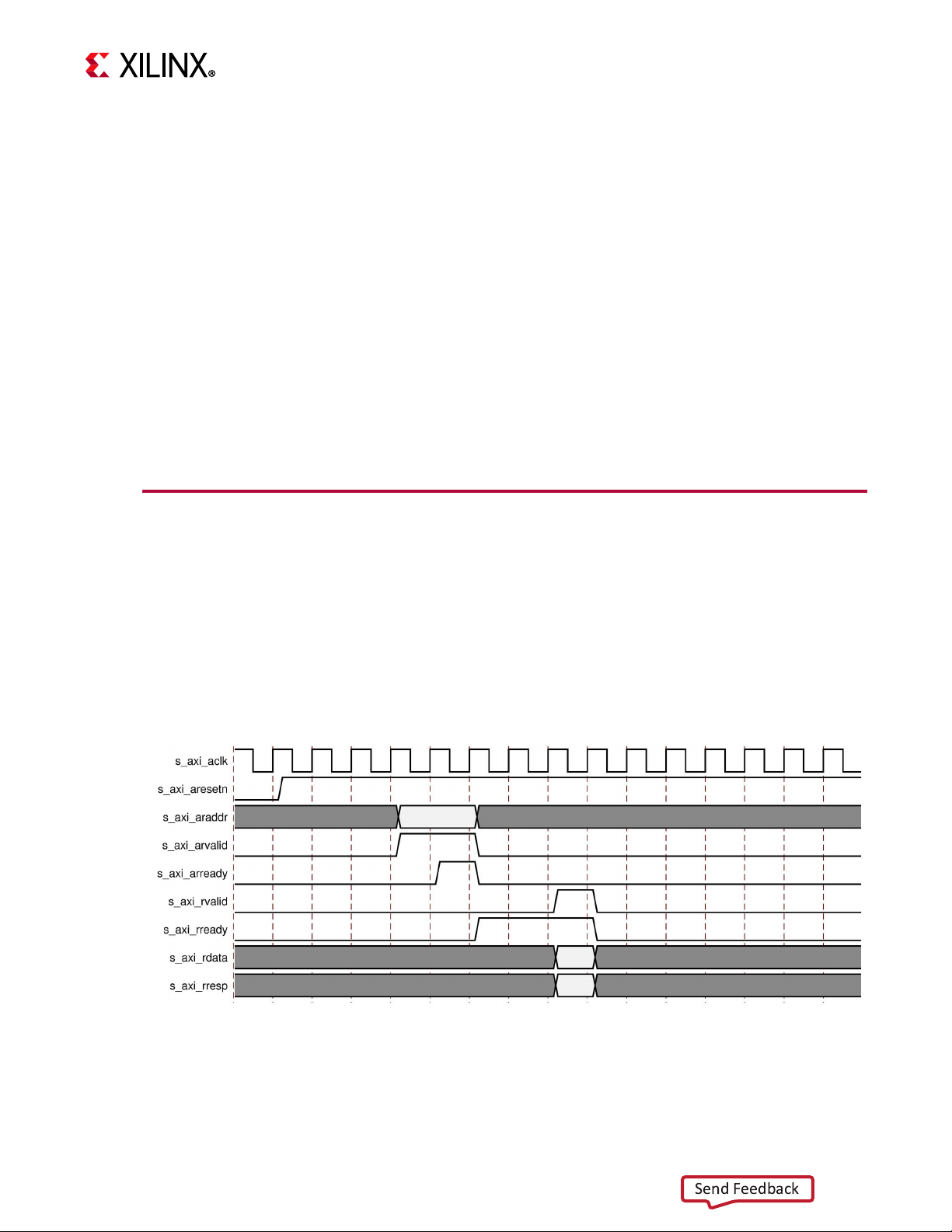
Appendix C: Debugging
Send Feedback
Action: Ensure the following for proper inter-operation. All CAN FD nodes in the
network must be programmed to have the following:
a. Same Arbitration Phase bit rate
b. Same Data Phase bit rate
c. Same Arbitration Phase Sample Point Position
d. Same Data Phase Sample Point Position
Requirements (c) and (d) come from the fact that CAN FD nodes perform bit rate
switching at the respective sample point. For more information on the CAN FD protocol
and other recommendations, see the standard specification and other white paper
references in the References, page 97.
If any of the listed requirements are not met, various frame errors can be seen when
performing the CAN FD communication.
Interface Debug
AXI4-Lite Interfaces
Read from a register that does not have all 0s as a default to verify that the interface is
functional. See Figure C-1 for a read timing diagram.
Note:
an example, and delays are not guaranteed to be the same as shown in the figure.
X-Ref Target - Figure C-1
Signals are compliant with AXI4-Lite protocol. The timing shown in Figure C-1 is provided as
CAN FD v2.0 94
PG223 December 5, 2018 www.xilinx.com
Figure C-1: AXI4-Lite Interface Read Timing Diagram
Page 95

Appendix C: Debugging
Send Feedback
Output s_axi_arready asserts when the read address is valid, and output
s_axi_rvalid asserts when the read data/response is valid. If the interface is
unresponsive, ensure that the following conditions are met:
•The s_axi_aclk and can_clk inputs are connected and toggling.
• The interface is not being held in reset, and s_axi_areset is an active-Low reset.
• The interface is enabled, and s_axi_aclken is active-High (if used).
• The main core clocks are toggling and that the enables are also asserted.
• If the simulation has been run, verify in simulation and/or in the Vivado Design Suite
debug feature capture that the waveform is correct for accessing the AXI4-Lite
interface.
CAN FD v2.0 95
PG223 December 5, 2018 www.xilinx.com
Page 96

Appendix D
Send Feedback
Additional Resources and Legal Notices
IMPORTANT: It is required to have a valid Bosch CAN FD protocol license before selling a device
containing the Xilinx CAN FD IP core.
Xilinx Resources
For support resources such as Answers, Documentation, Downloads, and Forums, see Xilinx
Support.
Documentation Navigator and Design Hubs
Xilinx® Documentation Navigator provides access to Xilinx documents, videos, and support
resources, which you can filter and search to find information. To open the Xilinx
Documentation Navigator (DocNav):
• From the Vivado® IDE, select Help > Documentation and Tutorials.
• On Windows, select Start > All Programs > Xilinx Design Tools > DocNav.
• At the Linux command prompt, enter docnav.
Xilinx Design Hubs provide links to documentation organized by design tasks and other
topics, which you can use to learn key concepts and address frequently asked questions. To
access the Design Hubs:
• In the Xilinx Documentation Navigator, click the Design Hubs View tab.
• On the Xilinx website, see the Design Hubs page.
Note:
on the Xilinx website.
For more information on Documentation Navigator, see the Documentation Navigator page
CAN FD v2.0 96
PG223 December 5, 2018 www.xilinx.com
Page 97

Appendix D: Additional Resources and Legal Notices
Send Feedback
References
These documents provide supplemental material useful with this product guide:
1. ISO 11898-1:2015: Road vehicles -- Controller Area Network (CAN) conformance test plan
– Part 1: Data link layer and physical signalling (https://www.iso.org/standard/
63648.html)
2. ISO 16845-1:2016: Road vehicles -- Controller Area Network (CAN) conformance test plan
– Part 1: Data link layer and physical signalling (https://www.iso.org/standard/
59166.html)
3. CAN with Flexible Data-Rate Specification version v1.0, Robert Bosch GmbH
4. CAN version 2.0A and B Specification, Robert Bosch GmbH
5. Mutter, Dr. Arthur. Robustness of a CAN FD Bus System – About Oscillator Tolerance and
Edge Deviations, Proceedings of the 14
2013
6. Vivado Design Suite User Guide: Designing with IP (UG896)
7. Vivado AXI Reference Guide (UG1037)
8. Vivado Design Suite User Guide: Designing IP Subsystems using IP Integrator (UG994)
9. Vivado Design Suite User Guide: Getting Started (UG910)
10. Vivado Design Suite User Guide: Logic Simulation (UG900)
11. ISE to Vivado Design Suite Migration Guide (UG911)
12. Vivado Design Suite User Guide: Programming and Debugging (UG908)
13. Vivado Design Suite User Guide: Implementation (UG904)
th
International CAN Conference, Paris, France,
CAN FD v2.0 97
PG223 December 5, 2018 www.xilinx.com
Page 98

Appendix D: Additional Resources and Legal Notices
Send Feedback
Revision History
The following table shows the revision history for this document.
Section Revision Summary
12/5/2018 Version 2.0
Compliance Testing in Appendix A Added information about ISO 16845-1:2016 conformance tests.
Tabl e 2- 1 Added APB Interface Signals to CAN FD Core I/O Signals table.
Added details for can_clk_x2.
Figure 4-1 Added explanations of new parameters in the Customize IP screen.
10/5/2016 Version 1.0
General updates • Added a note in Register Space section under Chapter 2,
Product Specification.
• Updated Automotive Applications Disclaimer in Please Read:
Important Legal Notices section.
11/18/2015 Version 1.0
N/A Initial Xilinx release.
Please Read: Important Legal Notices
The information disclosed to you hereunder (the "Materials") is provided solely for the selection and use of Xilinx produc ts. To t he
maximum extent permitted by applicable law: (1) Materials are made available "AS IS" and with all faults, Xilinx hereby DISCLAIMS
ALL WARRANTIES AND CONDITIONS, EXPRESS, IMPLIED, OR STATUTORY, INCLUDING BUT NOT LIMITED TO WARRANTIES OF
MERCHANTABILITY, NON-INFRINGEMENT, OR FITNESS FOR ANY PARTICULAR PURPOSE; and (2) Xilinx shall not be liable (whether
in co nt ract or t or t, in cluding ne gl ig en ce , o r under a ny other theory of liability) for any loss or damage of any kind or nature related
to, arising under, or in connection with, the Materials (including your use of the Materials), including for any direct, indirect,
special, incidental, or consequential loss or damage (including loss of data, profits, goodwill, or any type of loss or damage
suffered as a result of any action brought by a third party) even if such damage or loss was reasonably foreseeable or Xilinx had
been advised of the possibility of the same. Xilinx assumes no obligation to correct any errors contained in the Materials or to
notify you of updates to the Materials or to product specifications. You may not reproduce, modify, distribute, or publicly display
the Materials without prior written consent. Certain products are subject to the terms and conditions of Xilinx's limited warranty,
please refer to Xilinx's Terms of Sale which can be viewed at https://www.xilinx.com/legal.htm#tos; IP cores may be subject to
warranty and support terms contained in a license issued to you by Xilinx. Xilinx products are not designed or intended to be
fail-safe or for use in any application requiring fail-safe performance; you assume sole risk and liability for use of Xilinx products
in such critical applications, please refer to Xilinx's Terms of Sale which can be viewed at https://www.xilinx.com/legal.htm#tos.
AUTOMOTIVE APPLICATIONS DISCLAIMER
AUTOMOTIVE PRODUCTS (IDENTIFIED AS “XA” IN THE PART NUMBER) ARE NOT WARRANTED FOR USE IN THE DEPLOYMENT OF
AIRBAGS OR FOR USE IN APPLICATIONS THAT AFFECT CONTROL OF A VEHICLE (“SAFETY APPLICATION”) UNLESS THERE IS A
SAFETY CONCEPT OR REDUNDANCY FEATURE CONSISTENT WITH THE ISO 26262 AUTOMOTIVE SAFETY STANDARD (“SAFETY
DESIGN”). CUSTOMER SHALL, PRIOR TO USING OR DISTRIBUTING ANY SYSTEMS THAT INCORPORATE PRODUCTS, THOROUGHLY
TEST SUCH SYSTEMS FOR SAFETY PURPOSE S. USE OF P ROD UC TS IN A SAF ETY APPLICATION WITHOUT A SAFETY DESIGN IS FULLY
AT THE RISK OF CUSTOMER, SUBJECT ONLY TO APPLICABLE LAWS AND REGULATIONS GOVERNING LIMITATIONS ON PRODUCT
LIABILITY.
© Copyright 2015-2018 Xilinx, Inc. Xilinx, the Xilinx logo, Artix, ISE, Kintex, Spartan, Virtex, Vivado, Zynq, and other designated
brands included herein are trademarks of Xilinx in the United States and other countries. All other trademarks are the property of
their respective owners.
CAN FD v2.0 98
PG223 December 5, 2018 www.xilinx.com
 Loading...