

Page 1
Xilinx Automotive –
Flexible Solutions Beyond Silicon
AUTOMOTIVE
Page 2
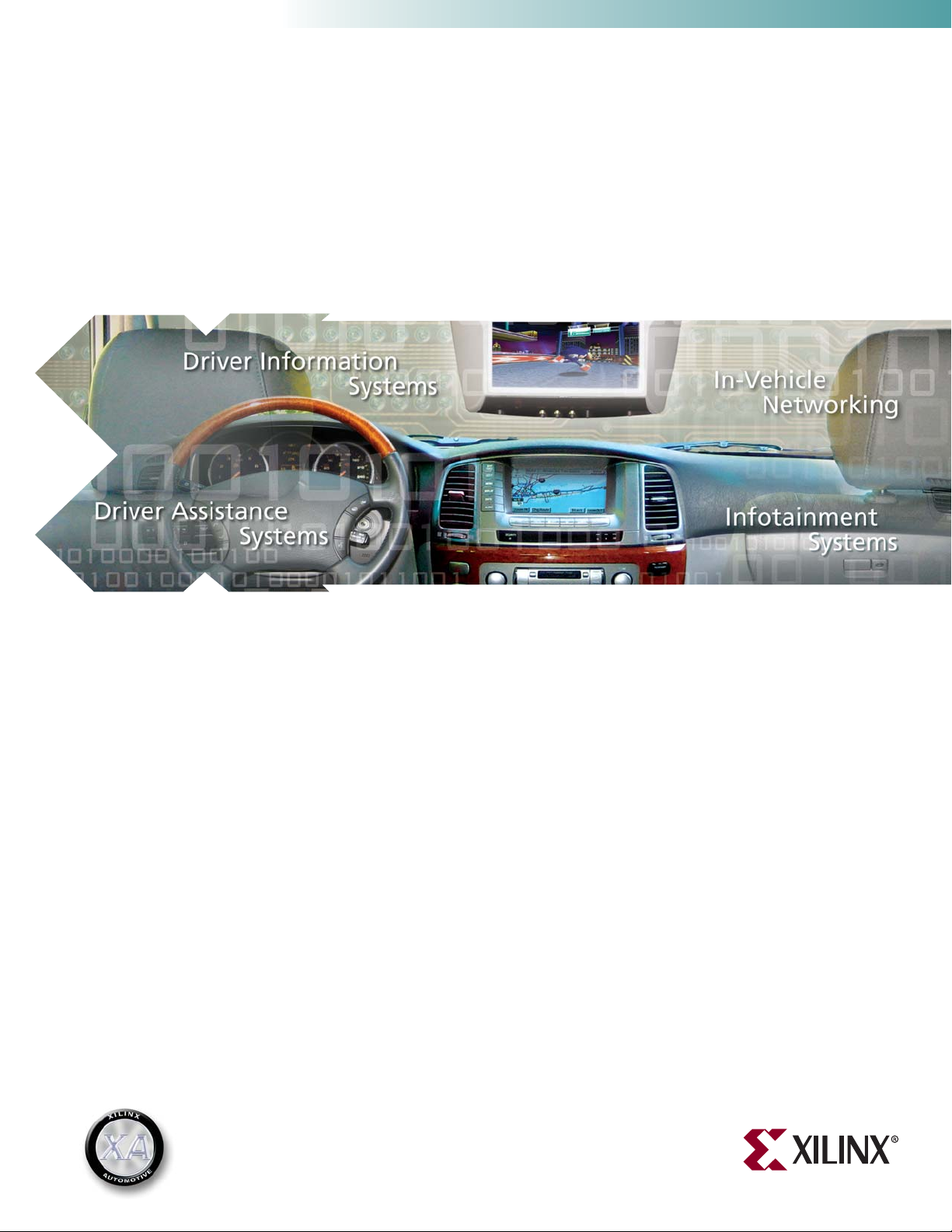
DRIVING AUTOMOTIVE
SOLUTIONS
Solutions Beyond Silicon
Xilinx leads one of the fastest-growing segments of the semiconductor industry––Programmable Logic
Devices (PLDs). With over 50 percent market share, Xilinx PLDs are rapidly becoming the solution of
choice for automotive applications, offering extreme flexibility, proven reliability, and the freedom to
change functionality even after being manufactured. As the automotive electronics market grows in the
areas of infotainment, driver assistance and driver information systems, Xilinx devices are at the heart of
each new innovation.
The Xilinx Automotive (XA) family of CPLDs and FPGAs allows for integration and
platform flexibility in design, lowering costs and eliminating obsolescence concerns,
while helping you achieve aggressive BOM cost targets.
To provide the complete solution, Xilinx is committed to develop, support and
™
maintain key automotive IP blocks through our LogiCORE
system.
Xilinx is also working with prominent third-party companies to offer further IP
modules, as well as the required operating system/software support. In addition,
custom development and system integration are offered through expert design
services by Xilinx, as well as by proven third-party providers.
Courtesy of Ibeo Automobile Sensor GmbH
Automotive Industry Standards
• ISO/TS16949 Automotive Certification
• AEC-Q100 Device Qualification
• RoHS Compliance
• Pb-Free Packaging
• Extended temperature ranges:
I-Grade (Tj= -40˚C to + 100˚C)
Q-Grade (Tj= -40˚C to +125˚C)
Automotive
Page 3
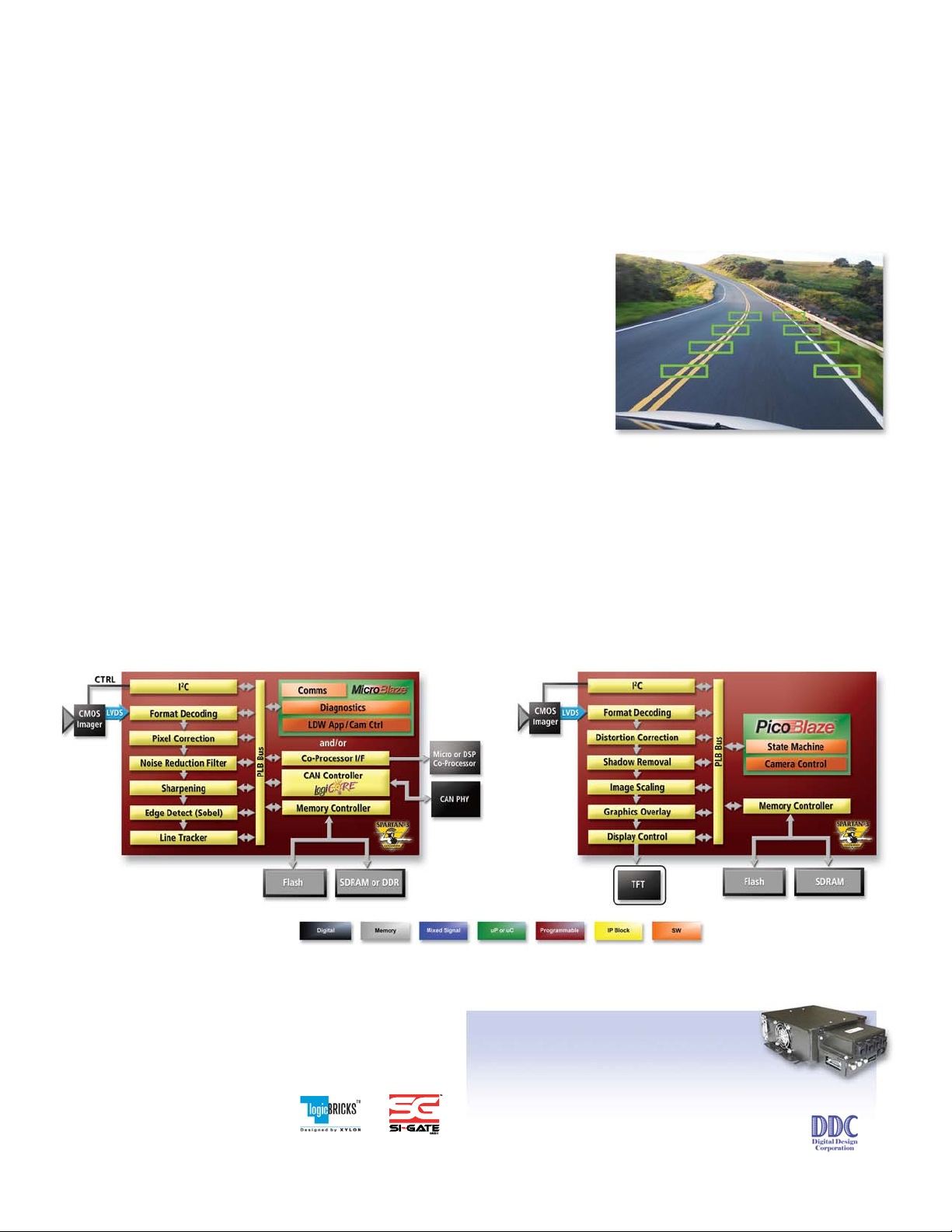
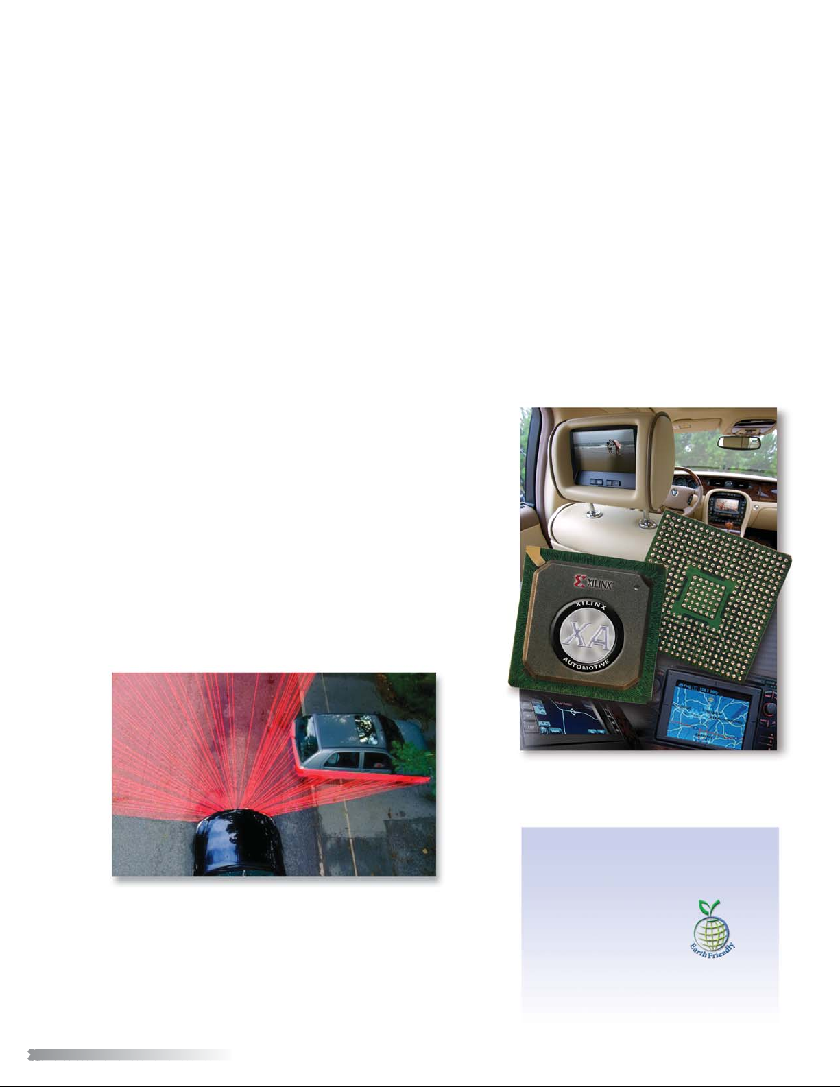
IMAGE PROCESSING
AND RECOGNITION
Xilinx Automotive FPGAs are being utilized as key components in the deployment of
vision-based Driver Assistance Systems:
• Superior computational performance to support pixel-level image processing
• Scalability for multiple feature bundling and customization on a single platform
• Flexibility for time-to-market and processing algorithm evolutionary enhancement
Xilinx Automotive and its alliance members offer a combination of image processing IP
solutions and design services tailored to automotive market needs:
• Productized IP cores provide fundamental image processing functionality and serve as
building blocks for customer-implemented designs
• Specialized design services leverage FPGA design experts with image processing experience
for efficient design and implementation efforts (turn-key or collaborative)
• Application-specific development boards for proof-of-concept implementation
Vision-based Automotive Applications
Forward-Looking Example: Lane Departure Warning Rear-Looking Example: Back-up/Park Aid
DDC's Automotive VADR module provides an
FPGA-based image processing platform with the
ability to record raw roadway video data in the field
for laboratory evaluation.
Page 4
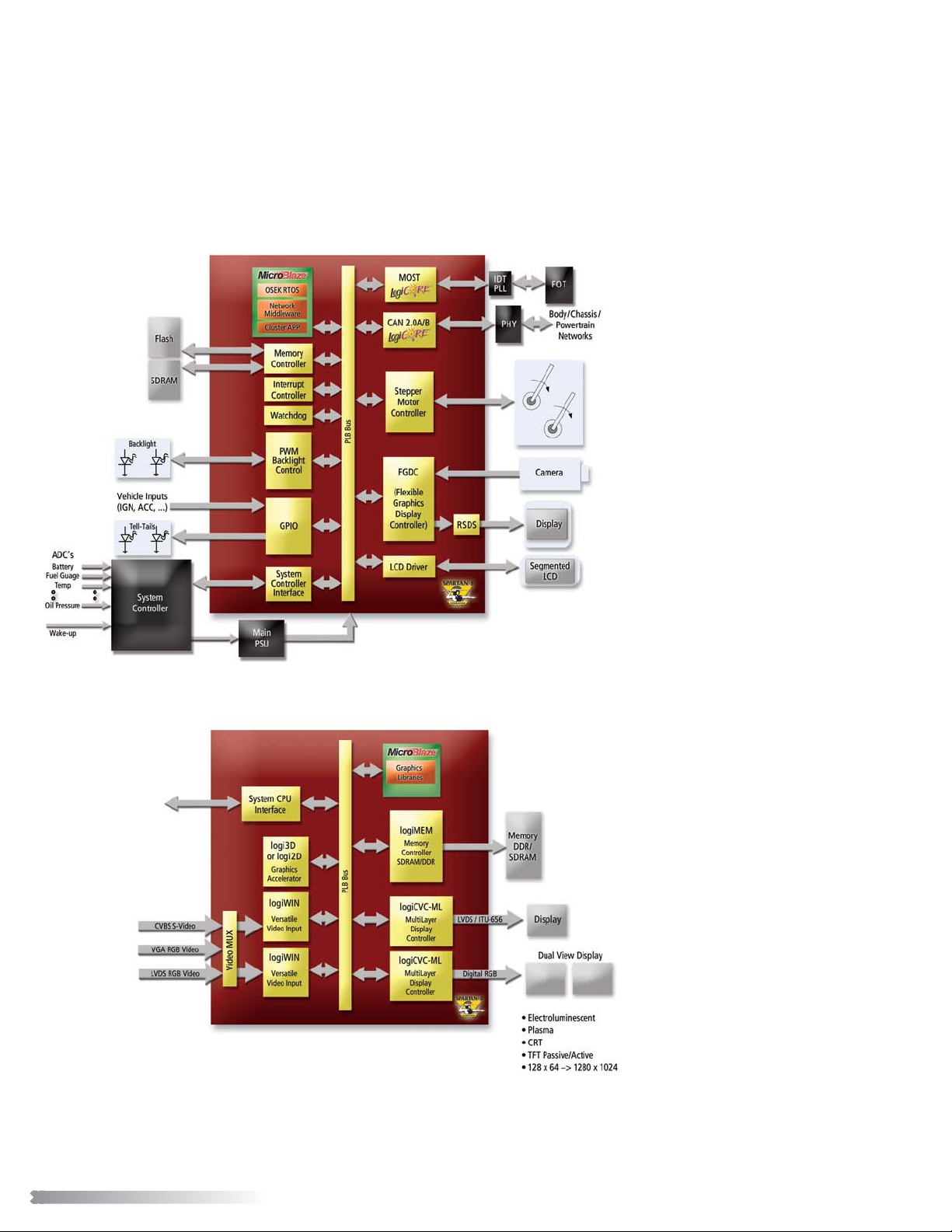
VIDEO AND GRAPHICS
Hybrid Instrument Cluster
Flexible Graphics Display
Controller System
Scalability and Flexibility
The scalability and flexibility of FPGAs can be
leveraged by the system architect in multiple ways.
For example, in driver information applications, the
increased usage of LED background lighting in today's
instrument clusters requires sophisticated control of
the individual LEDs to match the exact color and
brightness in OEM specifications.
Based on production variances of the LEDs, along with
varying numbers and arrangements inside the clusters,
achieving high production yields has become difficult
and now requires individual end-of-line programmability,
easily achievable with FPGA technology.
Easy LCD Interfacing
Deployment of hybrid instrument clusters consisting
of various numbers of traditional analog gauges,
with the addition of an LCD TFT display, poses further
challenges to the developer. Built-in support on
™
Spartan
differential I/O standards, such as Reduced Swing
Differential Signaling (RSDS), make external
terminating resistors obsolete by simultaneously
simplifying the physical connection between the
FPGA and the display.
-3 generation products for low-swing
Automotive
Different kinds of display connections, as well as
resolutions, can easily be overcome with the highly
scalable and flexible FPGA approach, covering a
complete range of needs from simple text, to 2D
animation, to graphics-intensive 3D representations.
Page 5
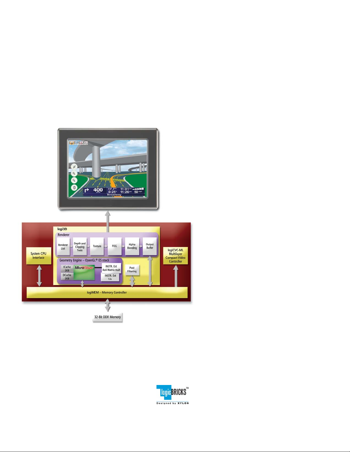
3D Graphics Accelerator
Xylon®Graphics Display Controller Solution
• Xylon Graphics Display Controller solution features a set of
configurable IP that is fully compatible with the Xilinx EDK
Platform Studio, allowing for complete systems with optional
™
Microblaze
coding required
• Xylon IP cores combined with a Spartan XA FPGA scale
very efficiently, thus making it possible to size the FPGA
to a particular end-product configuration, and optimize
cost-per-function without changing platform architecture
or board design
• Graphics subsystems can be assembled with the appropriate
features that are well suited to an entire range of low- to
high-performance graphics systems, with or without video
support, all at a competitive cost
• Scaling the number of displays to two or more in a system,
such as Rear-Seat Entertainment, is now possible on a
single FPGA
embedded processor with little, or no, VHDL
Supporting a Wide Range of Applications
• Low-end graphics systems, such as message centers or HVAC
control, requiring display functions such as blend, fade, scroll,
and simple animation of graphic objects through the use of a
multilayer alpha blended LCD controller and basic 2D
acceleration
• Mid/High-end graphics systems, such as fully reconfigurable
LCD instrument clusters or Rear-Seat Entertainment systems,
requiring additional operations such as bitmap decompression,
anti-aliased scalable fonts, bitmap rotation, and bitmap
translation/scaling
• High-end graphics systems, such as navigation or advanced
user interfaces, requiring real time manipulation of 3D graphics
including texture rendering, shading, or other true 3D effects
Xylon graphics software support ranges from basic embedded
graphic libraries (i.e. Segger emWIN) to complete end-to-end
development solutions including GUI development environments
(i.e. Altia) and industry standard interfaces (i.e. OpenGL ES).
Page 6

APPLICATION
DEVELOPMENT PLATFORMS
IogiCRAFT2
The logiCRAFT2 provides designers with an evaluation and development platform targeted for multidisplay automotive infotainment systems, such as rear-seat entertainment products. Using a completely
field-configurable platform, it combines the highly popular Xilinx MicroBlaze32-bit microprocessor core
together with a wide range of graphics and display controller IP modules from Xylon’s logicBRICKS
core family. Based on a Xilinx Spartan-3 FPGA 1.5 million system gate platform, it is capable of:
• Driving up to three different displays simultaneously, including configurable power supply voltages
for each, with different video streams on each display
• Supporting a wide variety of video input and output standards, including: LVDS, CMOS, digital and
analog RGB, COG and CVBS
• Providing complementary audio inputs and outputs, including infrared-based audio transmission for
wireless headphone utilization
• Connectivity to automotive bus systems, such as LIN, CAN and MOST®standards, as well as other
industry standards such as RS232, USB and Ethernet
™
IP
IogiCRAFT3
The logiCRAFT3 is derived from the logiCRAFT2 platform utilizing a smaller form factor, ideally to fit
behind a 7“ LCD, targeting single and remote display applications in the automotive environment.
It is based on a completely field-configurable platform combining the Xilinx MicroBlaze 32-bit microprocessor core together with the wide range of graphics and display controller IP modules from
Xylon’s logicBRICKS IP core offerings.
• The platform supports a wide variety of simultaneous video input and output standards, such as CVBS
or S-Video supporting PAL/NTSC/SECAM as well as one/two twisted pairs 1-wire LVDS based on APIX
by Inova—COG displays as well as different COG power supply requirements are also supported
• Audio input and output capabilities
• Connectivity is provided via CAN and RS232; in addition, it can be optionally extended with an Apple
iPod compatible serial interface, as well as a Bluetooth module based on Cambridge Silicon Radio
• Provisions to control a touch screen are also offered
XA1600E Board
The Automotive ECU Development Kit (HW-XA3S1600E-UNI-G) provides designers with a configurable
and expandable out-of-the-box platform, suitable for a wide range of Automotive applications. Due to
its small form factor, it can easily be placed in a standard metal housing. The board has also been
designed to be powered by a 12 volt power supply for in-vehicle prototype use.
• Powered by a completely field-configurable platform running on a Xilinx Spartan-3E FPGA, it combines
programmable logic for custom-driven IP applications as well as the popular Xilinx MicroBlaze 32-bit
microprocessor core
• Features robust memory subsystem containing on-board Flash and SRAM memory
• Supports standard Automotive and System-on-Chip peripherals including all necessary physical layers
on-board the ECU, such as JTAG, 10/100 Ethernet, USB 2.0, 12-bit ADC, High- and Low-Speed CAN,
™
FlexRay
, LIN, K-Line, UART, SPI and over 150 user programmable I/Os
Automotive
Page 7

Power Supply
Vehicle Connectivity
Voltage
Indicators
Board
PSU
COG PSU &
Sequencing
MOST IDT
PLL
2x
CAN PHY
2x
LIN PHY
FlexRay
PHY
Application Connectivity
Debug App.
RS232 PHY
Ethernet
PHY
USB OTG
PHY
Firewire
PHY
Memory and Configuration
CPLD
8 x LED
Remote Control
Switches
5 Push Buttons or 5x5
Key Matrix 8 DIP SW
Video Out 3
2 x
Tou ch Screen
Video Out 1 & 2
2 x VGA DAC,
Analog RGB
2 x DVI Tx
Video IN 1 & 2
2 x Video
Decoder
Video
MUX 4x2
2 x VGA ADC,
Analog
RGB
Video CLK
PLL
2 x DVI Rx
Audio
1/2 Stereo
CODEC ADC
1/2 Stereo
CODEC DAC
Stereo
Audio
MUX 4x2
2 x IR Stereo
Audio Channels
RST Ctrl.
OSC
33MHz
User Expansion Header
logiCRAFT2
PSU Conn
MOST
FOT
2 x DB9
Male
2 x DB9
Male
DB9
Male
DB9
Female
RJ45
MiniA/B
2x
Firewire
128MB/64-bit
DDRAM
8MB/16-bit
NOR Flash
Dia. RGB &
COG Ctrl.
Hirose DF11
2 x Resistive
Tou ch Screen
Conn.
2 x S-Video
CVBS
2 x DVI
2 x LVDS
Hirose DF11
2 x Digital
RGB
Hirose DF11
1 x LVDS
Hirose DF11
2 x S-Video
(4xCVBS)
2 x DVI
Digital RGB
Hirose FX2-60
2 x Mono Mic
Micro Jack
4 x Stereo Line
IN Micro Jack
2 x Stereo Line
Out Micro Jack
2 x Stereo
Headphones
Micro Jack
Hirose FX2-60
40 FPGA IOB
Hirose FX2-60
40 FPGA IOB
JTAG
3S1500
Automotive Grade Power Supply
Vehicle
Connectivity
Voltage
Indicators
Various Board
Supply Voltages
Board
PSU’s
High and Low
Side Switch
Inputs
High
and
Low
Side
Drivers
Switches
4 Push Buttons
or 8 DIP SW
Application Connectivity
Ethernet PHY
USB 2.0 PHY
User Expansion Header
XA1600E
External
Power Input
Vehicle Connection Port
D-SUB 44 Pin Male
Vehicle Connection Port
D-SUB 44 Pin Male
RJ45
RJ45
2x SMA
External
Clock
Socket
DIL8
160 Pin Molex
Connector
160 Pin Molex
Connector
JTAG
3S1600E
WAKEUP
JUMPERS
FUSE
WAKE CAN
WAKE LIN
VOLT1
VOLT2
VOLTX
WAKE BOARD
VEHICLE BATT
VEHICLE IGN
WAKE
DETECT
SPI
HSHSHS
HS
LSLSLS
LS
PWM IN
2x FlexRay PHY
HS CAN PHY
HS CAN PHY
LS CAN PHY
2x LIN PHY
K-Line PHY
16 ch 1 MSPS
12-bit A/D
Debug App.
RS232 PHY
16 CH
WAKE CAN
WAKE CAN
WAKE LIN
12 x LED
Port
Extender
LVDS TX DIFFERENTIAL PAIR
2x SMA
LVDS RX DIFFERENTIAL PAIR
2x SMA
LVDS CLK DIFFERENTIAL PAIR
2x SMA
LVDS CLK
LVDS CLK
SYNTHESIZER
SPI CONFIG
Memory and Configuration
1MB/16-bit
SRAM
32MB/32-bit
SDRAM
Xilinx Config
FLASH
8Mbit/16-bit
Serial NOR Flash
32 Mbit (4M x 8)
8MB/16-bit
NOR Flash
9536XL
CPLD
DATA/ADDRESS BUS
SPI
SLAVE PARALLEL (8 BIT)
CONFIG
MODE
Config Options:
– SPI
– Slave Parallel
Config Indicators
User Configurable PLL OSC 24MHz
SPI
PLL Config
CLK1
2C256 CPLD
CLK2
CPLD:
– Level Shifting
– Configuration
– Wake-up
Power Supply
Vehicle Connectivity
Video Out 1
Application Connectivity
Memory and Configuration
Voltage
Indicators
COG PSU &
SEQUENCING
LED
Backlight PSU
COG VCOM
GAMMA PSU
Video IN 1 & 2
Video
Decoder
Video
Decoder
Video
Amplifier
and
MUX 4x2
Video CLK
PLL
LVDS
Transceiver
Remote Control
logiCRAFT3
Digital RGB
Hirose FX2-60
Audio
Stereo
Audio
Amplifier
MUX 4x2
Mono Mic
PCB Pad
4x Stereo Line
IN 4x RCA and
4vx PCB Pads
Stereo Line
Out PCB Pad
2 x IR Stereo
Ch. Hirose DF11
Stereo
Headphones
PCB Pad
1/2 Stereo
CODEC ADC
1/2 Stereo
CODEC DAC
RST Ctrl.
OSC 33MHz
JTAG
Board
PSU
PSU Conn
Hirose DF11
CAN
PHY
DB9 Male
CAN
PHY
CVBS
Encoder
DB9 Male
3S250E, 3S500E or 3S1200E
Dig. RGB & COG
Ctrl. Hirose DF11
S-Video CVBS
2xRCA
LVDS
Hirose DF11
2x S-Video,
(4xCVBS)
4 x RCA
5 Pin .1”
single row
header
To iPod
Hirose
DF11
Hirose
DF11
To
Bluetooth
Module
DB9 Female
BPI Config
8 GPIO’s
16MB/32-bit
SDRAM
8MB/8-bit
NOR Flash
GPIO
Extender
Debug App.
RS23
PHY
Tou ch
Screen
Page 8

XILINX AUTOMOTIVE --
Image Processing and Recognition
Xilinx and its alliance members offer solutions beyond silicon by providing IP building blocks and design
services in the areas of image processing and recognition. This allows for faster development and product
differentiation for driver assistance applications, including:
• Night Vision
• Lane Departure Warning
• Park Assist
• Back Guide Monitor
• Adaptive Cruise Control
• Drowsy Driver Detection
Courtesy of Robert Bosch GmbH
Video and Graphics
Offerings of key IP building blocks and design services allow for highly scalable
and cost-efficient implementations of infotainment and driver information
systems, including:
• Head-Unit
• Rear-Seat Entertainment
• TV Tuner
• Audio/Multimedia Systems
• Game Consoles
• Hybrid Instrument Cluster
• Heads-up Display
Application Development Platforms
Off-the-shelf, application-specific development platforms are available to provide developers a quick start,
and serve as a comprehensive hardware base to satisfy their expectations. Currently available are:
• Automotive ECU Development Kit (HW-XA3S1600E-UNI-G)
• logiCRAFT2—Infotainment Development Platform
• logiCRAFT3—Compact Multimedia Display Development Platform
• VADR—Image Processing Development Platform
Automotive
Page 9

Xilinx Technology Leadership
Xilinx leads the way in Programmable Logic Devices (PLDs), one of the fastest growing
segments of the semiconductor industry.
• Inventing and driving the technology of the Field Programmable Gate Array (FPGA)
• Offering highly scalable and flexible devices, where features and functions can be
changed “on the fly,“ or upgraded in the field
•
Supplying more than 50% of the market for these devices today
• Expert design services through Xilinx and third party providers
• Full compliance and certification to ISO-9001,
ISO-14001 and ISO/TS16949
Xilinx Automotive Products
Xilinx Automotive solutions are driven by
a dedicated automotive product line,
based on:
• Pin-compatible products in various densities and packages suited for
automotive applications
• AEC-Q100 qualified products
• Production Part Approval Process (PPAP) documentation for all XA products
• A continuous improvement strategy
• Active membership in the Automotive Electronics Council (AEC) Technical
Specification Committee
• Associate membership in AUTOSAR, JASPAR, MOST Cooperation and
FlexRay Consortium
Vehicle Networking
Xilinx has designed, and is directly supporting, key automotive-specific
network interfaces. Xilinx works together with leading industry companies
to provide customers access to a comprehensive solution.
Page 10

VEHICLE NETWORKING
This super-set block diagram of an infotainment rear-seat
entertainment application shows a possible set-up based on
the combination of a host or digital signal processor (DSP)
together with an FPGA. In this example, the FPGA acts as
a companion chip to the host, providing multiple functions,
such as audio/video processing acceleration, a graphics
sub-system, and different user and vehicle networking
connections, such as CAN and MOST.
Flexible MOST Architecture_your design, your way
The following overview outlines four architectural options
showing how various components within the Xilinx solution
for MOST, including the MOST Network Interface Controller
(NIC), can be utilized to realize efficient system architectures.
There are many possible combinations that are not constrained
by fixed or predetermined interfaces, but can be
freely defined based on the desired overall system
architecture.
1. Off-loading the host processor by utilizing
the MicroBlaze processor to run the full
MOST Network Services software stack
along with OEM-specific FBlocks and High-
Level-Protocols in conjunction with the
OS8104 (PCM IP) or OS81050 (MLB IP).
2. Utilization of available LogiCORE IP to
completely eliminate the need for an external
MOST network controller.
3. Addition of direct access to the synchronous
MOST channels to perform pre- or post-
processing of incoming or outgoing data in
FPGA hardware without the need for any
software overhead.
4. Connectivity to a wide range of different
host interfaces.
Automotive
Page 11

MOST Solution
MOST IP
Object Layer
Transmit
Buffer
32 bit
OPB or
PLBv46
Bus
Supported XA Device Families Spartan-3, Spartan-3E, Spartan-3A, Spartan-3A DSP
Resources Used 7 4049-4117 2535-2580 6 2930-2990
* Represent typical slice count for Spartan-3 generation devices. Results will vary on device utilization and ISE options
Config
Registers
User Interface (UI)
Receive
Buffer
Local Link
RX
Streaming
Port
Local Link
TX
Streaming
Port
Transfer Layer
Transmit
Media
Access
Control
Processing
MOST IP Specifics
I/O LUTs FFs Block RAMs Slices*
Control
Receive
Routing Control
Media
Access
Control
TX
MCLK
Bypass
RCLK
RX
The LogiCORE IP for the Media Oriented Systems Transport (MOST) is a complete
NIC supporting the MOST Specification revision 2.4 or later for the MOST25
network. Capabilities include:
FOT
MOST Ring
• Compatible with SMSC 8104(A), OS8105x (INIC) and Analog Devices
MXVR transceivers
• Direct interface to MOST ring via IDT PLL (IDT5V80001) for clock
FOR
generation/recovery and the fiber optic transceiver (FOT)
• Operates in both master and slave modes
IDT PLL Clock Generation/Recovery and Network Bypass
• Synchronous, asynchronous, and control channels with 4-60 bytes of
synchronous data per frame including support of up to full bandwidth
sustained transfers (24 Mbps)
• Streaming port allows synchronous data co-processing with low host
controller overhead
• Full support of error and status notification including support for ring break
diagnosis test
• Supported in CORE Generator
EDK for MicroBlaze-based ECU applications
™
software for stand alone applications and in
Layer 7 Application
Layer 6 Presentation
Layer 5 Session
Layer 4 Transport
Layer 3 Network
Layer 2 Data Link
Layer 1 Physical
Application
(ET)
(NB)
Enhanced-
NetBlock FBlock
Command Interpreter (MCI)
Application
Control Message Service (CMS)
NetworkMaster
Testabilty FBlock
(SCS)
(AMS)
Control Service
Streaming Data
Message Service
Network Interface Controller Abstraction
Optical/electrical converters, connectors and optical fiber
HLP’s (Software Download, Diagnostics,etc)
FBlocks
MOST Network Services Layer 2 API
(NMS)
FBlock (NM)
Shadow FBlock
NetworkMaster
Address Handler Service
MOST Network Services Layer 1 API
Service (RAS)
Remote Access
Control (SIC)
Streaming Data Interface
Low-Level Driver
MOST Network Interface Controller
(AHS)
(MNTFS)
Notification Service
Transceiver
Control Service
Packet Service (PKS)
(XCS)
Supervisor L2
Power Master (PM)
Supervisor L1
(MSV)
Interface Control
(MSV2)
Optical
(OIC)
Network Service
L2 (NSV2)
Network
Service L1
(NSV)
Working closely with Mocean Laboratories AB, and the MOST Cooperation, Xilinx
enables a portable and highly modular MOST solution where applications can
be moved between NICs without source code modification. The MOST solution
is comprised of:
• Full software stack (up to MOST Specification revision 2.5) supporting Xilinx
solution for MOST
• Versions also available supporting SMSC OS8104(A) and OS8105x (INIC)
for MicroBlaze processor
• All services and protocols standardized in the MOST Cooperation are supported
• MOST Cooperation and several OEM FBlocks and High-level Protocol Modules
available including source code
• Fully linked/structured electronic documentation
• ANSI-C Source code with automated documentation generation
• Browse documentation using Service, Module, Function or Variable views
• Application examples library available as source code
Page 12

CAN Solution Fle
32 bit
OPB or
PLBv46
Bus
CAN IP
Object Layer
Transmit
Buffer
Transmit
High
Priority
Buffer
Receive
FIFO
Configuration
User Interface (UI)
Supported XA Device Families
Resources Used
* Represent typical slice count for Spartan-3 generation devices. Results will vary on device utilization and ISE options
TX
Priority
Logic
Registers
Acceptance
Filtering
CAN IP Specifics
Spartan-3, Spartan-3E, Spartan-3A, Spartan-3A DSP
I/O LUTs FFs BlockRAMs Slices*
3 868-1056 411-593 2 569-885
Transfer Layer
Bit Stream
Processor
Bit Timing
Module
CLK
TX
RX
CAN PHY
The LogiCORE IP for the Controller Area Network (CAN) is a
controller compliant to ISO 11898-1, CAN 2.0A and CAN 2.0B
standards. It provides characteristics such as:
• Validated at C&S group
• Supports bit rates of up to 1 Mbps
• Supports both standard (11-bit identifier) and extended
CAN Bus
(29-bit identifier) frames
• Transmit and receive message FIFOs with user-configurable
depths of up to 64 messages
• Transmit prioritization through one High-Priority Transmit buffer
• Acceptance filtering (user-configurable number) of up to
4 acceptance filters
• Maskable Error and Status Interrupts
• Supported in CORE Generator software for stand alone applications
and in EDK for MicroBlaze-based ECU applications
Working closely with Vector, the availability of the CAN Driver for
the Xilinx MicroBlaze 32-bit processor, enables easy access to the
full suite of Vector’s CANbedded Software solution.
Application
Communication
Control
Layer
CAN
Interaction
Layer
Network
Management
Diagnostics
Transport Protocol
CAN Driver
Xilinx LogiCORE IP CAN Controller
Transceiver
Courtesy of Vector Group
Universal
Measurement
and Calibration
Protocol
• The CAN Driver handles the hardware-specific characteristics
of the Xilinx FPGA and provides the initialization, wakeup
detection, transmission and reception of messages with
data—and functional interface data—and functional
notification including indication and confirmation as
well as overrun and error handling
Configuration
Tool
• Provision of a standardized application
interface to the higher level software modules
as the interaction layer, transport protocol,
network management, universal measurement
and calibration protocol also available through Vector
• Several diagnostics layers available in accordance with
ISO14229 (UDS) and ISO14230 (Keyword Protocol 2000)
• Full integration into the Vector tools chain including flash
programming, operating system, database and debug tools
Automotive
Page 13

FlexRay Solution
32 bit
OPB or
PLBv46
Bus
FlexRay IP
User Interface (UI)
Controller Host
Interface
Transmit
Buffer
Config/
Status
Register
Config/
Status
Register
Receive
FIFO
Protocol Engine (PE)
Media
Access
Control
Protocol
Operation
Control
Frame &
Symbol
Proc.
Bit
Stream
Engine
Clock
Sync
Wakeup
& Start
Bit
Stream
Decode
FlexRay IP Specifics
Supported XA Device Families
Resources Used
* Represent typical slice count for Spartan-3 generation devices. Results will vary on device utilization and ISE options
Spartan-3, Spartan-3E, Spartan-3A, Spartan-3A DSP
I/O LUTs FFs Block RAMs Slices*
5 5506-6587 3179-3386 9 to 18 4028-4789
TX
TX_EN
RX
FlexRay PHY
FlexRay Bus
The LogiCORE IP for FlexRay is a controller that implements the
FlexRay communication protocol as defined in the FlexRay Protocol
Specification v2.1 Rev A. It provides functionalities such as:
• Data rate of up to 10 Mbps
• Single Communication Channel
• Scalable synchronous and asynchronous data transmission
• Configurable payload length up to a maximum of 256 bytes
• Configurable receive and transmit buffers for storage of up to
128 messages each
• Frame ID, cycle counter and message ID based receive filtering
• OPB and PLB interface suitable with single and burst support
• Variable OPB and PLB interface clock
• Supported in CORE Generator software for stand alone
applications and in EDK for MicroBlaze-based ECU applications
Software
Component
Software
Component
Software
Component
Software
Component
Software
Component
AUTOSAR Runtime Environment (RTE)
Diagnostic
Communication
Manager
PDU Router
FlexRay
Transport
Protocol
AUTOSAR OS
Development
Error Tracer
ECU State
Manager
Diagnostic
Event
Manager
Communication
Manager
FlexRay
State
Manager
NM
Interface
FlexRay
Network
Management
FlexRay Interface
AUTOSAR COM
FlexRay Driver
Xilinx LogiCORE IP FlexRay Controller
FlexRay
Vector AUTOSAR BSW BSW of FlexRay-Stack XCP Communication AUTOSAR AUTOSAR ECU AUTOSAR ECU
Module Service Layer Abstraction Layer Microcontroller
Courtesy of Vector Group
Software
Component
XCP Protocol
Layer
XCP Transport
Layer
on FlexRay
Transceiver
Driver
Abstraction Layer
Availability of the FlexRay Driver for the Xilinx MicroBlaze
32-bit processor enables easy access to the full suite of
Vector’s FlexRay software solution developed according to
the AUTOSAR specification.
• The FlexRay Driver handles the hardware-specific
characteristics of the Xilinx FPGA and acts as an abstraction
layer to other software offerings available through Vector,
covering the signal, diagnostic and transport layer as well
as the network support and node management
• Full support of the FlexRay synchronous layer for the
driver as well as support of the FlexRay asynchronous
layer for the protocol stack and the application
• Full integration into the Vector tool chain including the
DaVinci Network Designer for FlexRay supporting multiple
FIBEX revisions, the development & analysis tool with
real-time support, as well as measurement and calibrations
of ECUs
Page 14

XILINX AUTOMOTIVE
1. System Gates include 20%-30% of CLBs used as RAMs. 2. Each slice comprises two 4-input logic function generators (LUTs), two storage elements, wide-function multiplexers, and carry logic.
Integrated in the DSP48A slices (Advanced Multiply Accumulate element). 4. Temperature Range Automotive I (T
j
= -40°C to +100°C); Automotive Q (T
j
= -40°C to +125°C)
Notes:
Part Number
Logic Cells
CLB Flip-Flops
VQG100 16 x 16 mm
Block RAM Blocks
Total Block RAM (Kbits)
Digital Clock Managers
(DCMs) Spartan-3, (DLLs) Spartan-IIE
Maximum Single Ended I/Os
Maximum Differential I/O Pairs
I/O Standards Supported
Dedicated Multipliers
DSP48A Slices
Device DNA Security
Temperature Range
(4)
Speed Grade
Maximum Distributed RAM (Kbits)
RoHS (Pb-free)
XA Released
Configuration Memory Bits (Mbits)
Slices
(2)
Logic Resources
Memory Resources
Clock Resources
I/O Resources
Embedded Hard
IP Resources
Configuration
Miscellaneous
TQG144 22 x 22 mm
PQG208 30.6 x 30.6 mm
FTG256 17 x 17 mm
FGG456 23 x 23 mm
FGG676 27 x 27 mm
System Gates
(1)
102 102
182182182
Spartan-IIE
XA2S50E
768
50K
1,728
1,536
8
32
4
102
28
—
—
—
I, Q
-6
XA2S100E
1,200
100K 150K 200K
2,700
2,400
10
40
4
102
28
—
—
—
I, Q
-6
XA2S150E XA2S200E
1,728
3,888
3,456
12
48
4
182
83
LVTTL, LVCMOS25, LVCMOS18, HSTL Class I, HSTL Class III,
HSTL Class IV, PCI 3.3V 32 - 33MHz, PCI-X 3.3V, SSTL3 Class I,
SSTL3 Class II, SSTL2 Class I, SSTL2 Class II,
AGP-2x, CTT, LVDS, Bus LVDS, LVPECL25 & 33
—
—
—
I, Q
-6
2,352
5,292
4,704
24 37 54 73
14
56
4
182
83
—
—
—
I, Q
-6
No No No No
Yes Yes Ye s Yes
0.6 0.9 1.1 1.4
300K
XA2S300E
3,072
6,912
6,144
96
16
64
4
182
83
—
—
—
I, Q
-6
No
Yes
1.9
XA3S50
Spartan-3
XA3S200 XA3S400 XA3S1000 XA3S1500
768 1,920 3,584 7,680 13,312
50K 200K 400K 1000K 1500K
1,728 4,320 8,064 17,280 29,952
1,536 3,840 7,168 15,360 26,624
412162432
72 216 288 432 576
2444 4
124 173 264 333 487
56 76 116 149 221
412162432
63 63
———— —
———— —
I, Q I, Q I , Q I, Q I
-4 -4 -4 -4 -4
12 30 56 120 208
Yes Yes Yes Yes Yes
Yes Yes Yes Yes Yes
0.4 1.0 1.7 3.2 5.2
97
124 141 141
173 173 173
264 333 333
487
LVTTL, LVCMOS33, LVCMOS25, LVCMOS18, LVCMOS15,
LVCMOS12, GTL, GTL+, HSTL15 Class I, HSTL15 Class III,
HSTL18 Class I, HSTL18 Class II, HSTL18 Class III, PCI 3.3V
32/64bit 33MHz, SSTL2 Class I, SSTL2 Class II, SSTL18
Class I, Bus LVDS, LDT (ULVDS), LVDS_ext, LVDS25 & 33,
LVPECL25, RSDS25
66
158
66
158
172 190 190
FGG484 23 x 23 mm
376
FGG400 21 x 21 mm
304 304
108 108
CPG132 8 x 8 mm
839292
Spartan-3E
XA3S100E
960
100K
2,160
1,920
4
72
2
108
40
4
—
—
I, Q
-4
XA3S250E
2,448
250K
5,508
4,896
12
216
4
172
68
12
—
—
I, Q
-4
XA3S500E
4,656
500K 1200K 1600K
10,476
9,312
20
360
4
190
77
20
—
—
I, Q
-4
XA3S1200E XA3S1600E
8,672
19,512
17,344
28
504
8
304
124
LVTTL, LVCMOS33, LVCMOS25, LVCMOS18, LVCMOS15,
LVCMOS12, HSTL18 Class I, HSTL18 Class III, PCI 3.3V
32/64bit 33MHz, PCI-X 3.3V, SSTL2 Class I, SSTL18 Class I,
Bus LVDS, LVDS25, LVPECL25, Mini-LVDS25, RSDS25
28
—
—
I, Q
-4
14,752
33,192
29,504
15 38 73 136 231
36
648
8
376
156
36
—
—
I, Q
-4
Yes Yes Ye s Ye s Ye s
Yes Yes Ye s Ye s Ye s
0.6 1.4 2.3 3.8 6.0
Package Area Maximum User I/Os
VQFP Packages (VQ): very thin QFP (0.5 mm lead spacing)
Chip Scale Packages (CP): wire-bond chip-scale BGA (0.5 mm ball spacing)
TQFP Packages (TQ): thin QFP (0.5 mm lead spacing)
PQFP Packages (PQ): wire-bond plastic QFP (0.5 mm lead spacing)
FGA Packages (FT): wire-bond fine-pitch thin BGA (1.0 mm ball spacing)
FGA Packages (FG): wire-bond fine-pitch BGA (1.0 mm ball spacing)
DEVICES
FPGAs
Automotive
Page 15

1. System Gates include 20%-30% of CLBs used as RAMs.
2. Each slice comprises two 4-input logic function generators (LUTs), two storage elements,
wide-function multiplexers, and carry logic.
3. Integrated in the DSP48A slices (Advanced Multiply Accumulate element).
4. Temperature Range Automotive I (T
j
= -40°C to +100°C); Automotive Q (Tj = -40°C to +125°C).
Notes:
XA3S200A
Spartan-3A Spartan-3A DSP
XA3S400A XA3S700A XA3S1400A XA3SD1800A
Part Number
1,792 3,5845,888 11,264 16,640
200K 400K 700K 1400K 1800K
4,032 8,064 13,248 25,344 37,440Logic Cells
3,584 7,168 11,776 22,528 33,280CLB Flip-Flops
16 20 20 32 84
288 360 360 576 1,512
4488 8
195 311 372 375 519
90 142 165 165 227
LVTTL, LVCMOS33, LVCMOS25, LVCMOS18, LVCMOS15, LVCMOS12, HSTL15
Class I, HSTL15 Class III, HSTL18 Class I, HSTL18 Class II, HSTL18 Class III,
PCI 3.3V 32/64bit 33MHz, PCI-X 3.3V, SSTL3 Class I, SSTL3 Class II, SSTL2
Class I, SSTL2 Class II, SSTL18 Class I, SSTL18 Class II, Bus LVDS, LVDS25 & 33,
LVPECL25 & 33, Mini-LVDS25 & 33, RSDS25 & 33, TMDS25 & 33, PPDS25 & 33
Block RAM Blocks
Total Block RAM (Kbits)
Digital Clock Managers (DCM)
Maximum Single Ended I/Os
Maximum Differential I/O Pairs
I/O Standards Supported
XA3SD3400A
23,872
3400K
53,712
47,744
126
2,268
8
469
213
28 56 92 176 260Maximum Distributed RAM (Kbits) 373
Slices
(2)
Logic Resources
Memory Resources
Clock Resources
I/O Resources
195FTG256 17 x 17 mm 195
FGG400 21 x 21 mm
311 311
FGG484 23 x 23 mm
372 375
FGG676 27 x 27 mm 519 469
CSG484 19 x 19 mm 309 309
System Gates
(1)
Package Area Maximum User I/Os
16 20 20 32 84
(3)
Dedicated Multipliers
———— 84
DSP48A Slices
Yes Ye s Ye s Yes Yes
Device DNA Security
I, Q I, Q I, Q I, Q I , Q
Temperature Range
(4)
-4 -4 -4 -4 -4
Speed Grade
126
(3)
126
Yes
I
-4
Yes Ye s Ye s Yes Ye s
RoHS (Pb-free)
Yes
No No No No No
XA Released
No
1.2 1.9 2.7 4.88.2
Configuration Memory Bits (Mbits)
11.7
Embedded Hard
IP Resources
Configuration
Miscellaneous
FGA Packages (FT): wire-bond fine-pitch thin BGA (1.0 mm ball spacing)
Chip Scale Packages (CS): wire-bond chip-scale BGA (0.8 mm ball spacing)
FGA Packages (FG): wire-bond fine-pitch BGA (1.0 mm ball spacing)
FPGAs
Dedicated Automotive Product Line
Choose from our wide range of pin-compatible AEC-Q100
qualified products in various densities and packages suited
for automotive applications.
Offering extreme flexibility and reliability, our dedicated
XA products are at the heart of innovation.
Logic Resources
Clock Resources
I/O Resources
Speed Grades
Product Term Clocks per Function Block
Output Voltage Compatible (V)
Min. pin-to-pin Logic Delay (ns)
Miscellaneous
Part Number
System Gates
Product terms per Macrocell
Global Clocks
Maximum I/O
Input Voltage Compatible (V)
Automotive I Speed Grades
Automotive Q Speed Grades
Temperature Grades
RoHS (Pb-free)
XA Released
Package Area
VQFP Packages (VQ): very thin QFP (0.5 mm lead spacing)
VQG44 12 x 12 mm
VQG64 12 x 12 mm
VQG100 16 x 16 mm
TQFP Packages (TQ): thin QFP (0.5 mm lead spacing)
TQG100 16 x 16 mm
TQG144 22 x 22 mm
Chip Scale Packages (CP): wire-bond chip-scale BGA (0.5 mm ball spacing)
CPG132 8 x 8 mm
Chip Scale Packages (CS): wire-bond chip-scale BGA (0.8 mm ball spacing)
CSG144 12 x 12 mm
1. Temperature Range Automotive I (Ta = -40°C to +85°C); Automotive Q (Ta = -40°C to +105°C with Tj maximum = +125°C).
Notes:
2. Area dimensions for lead-frame products are inclusive of the leads.
Macrocells
(2)
CPLDs
XA9500XL Family
XA9536XL
XA9572XL
800
1,600
36
90
3
18
34
2.5/3.3/5
2.5/3.3/5
2.5/3.3
2.5/3.3
15.5
-15
-15
(1)
I, Q I, Q I
Yes Ye s Ye s
Yes Ye s Ye s
34
15.5
-15
-15
CoolRunner-II Family
XA95144XL
72
90
3
18
72
2.5/3.3/5
34
52
72
3,200
144
90
18
117
XA2C32A
750 1,500 3,000 6,000 9,000
3
XA2C64A XA2C128 XA2C256 XA2C384
32 64 128 256 384
56 56 56 56 56
33333
16 16 16 16 16
33 64 100 118 118
1.5/1.8/2.5/3.3 1.5/1.8/2.5/3.3 1.5/1.8/2.5/3.3 1.5/1.8/2.5/3.3 1.5/1.8/2.5/3.3
1.5/1.8/2.5/3.3 1.5/1.8/2.5/3.3 1.5/1.8/2.5/3.3 1.5/1.8/2.5/3.3 1.5/1.8/2.5/3.3
2.5/3.3
15.5
-15
-15
5.5 6.7 7.0 7.0 9.2
-6 -7 -7 -7 -10
-7 -8 -8 -8 -11
I, Q I, Q I, Q I, Q I, Q
Yes Yes Ye s Yes Ye s
Yes Yes Ye s Yes Ye s
Maximum User I/Os
33 33
64 80 80
117
118 118
100
Page 16

Corporate Headquarters
Xilinx, Inc.
2100 Logic Drive
San Jose, CA 95124
USA
Tel: 408-559-7778
Web: www.xilinx.com
Europe
Xilinx Europe
One Logic Drive
Citywest Business Campus
Saggart, County Dublin
Ireland
Tel: +353-1-464-0311
Web: www.xilinx.com
Japan
Xilinx K.K.
Art Village Osaki Central Tower 4F
1-2-2 Osaki, Shinagawa-ku
Tokyo 141-0032 Japan
Tel: +81-3-6744-7777
Web: japan.xilinx.com
TAKE THE NEXT STEP
For more information on Xilinx automotive solutions,
visit
www.xilinx.com/automotive
Asia Pacific Pte. Ltd.
Xilinx, Asia Pacific
5 Changi Business Park
Singapore 486040
Tel: +65-6407-3000
Web: www.xilinx.com
.
www.xilinx.com
Copyright © 2007 Xilinx, Inc. All rights reserved.
XILINX, the Xilinx Logo, and other designated
brands included herein are trademarks of
Xilinx, Inc. PowerPC is a trademark of IBM,Inc.
All other trademarks are the property of their
respective owners.
Printed in U.S.A. PN 2055
 Loading...