

Winbond Electronics W77E468F-25, W77E468F-40 Datasheet

Preliminary W77E468
8 BIT MICROCONTROLLER
Table of Contents--
GENERAL DESCRIPTION..............................................................................................................................2
FEATURES......................................................................................................................................................2
PIN CONFIGURATION....................................................................................................................................3
BLOCK DIAGRAM...........................................................................................................................................4
PIN DESCRIPTION..........................................................................................................................................5
FUNCTIONAL DESCRIPTION ........................................................................................................................6
PROGRAMMABLE TIMERS/COUNTERS....................................................................................................54
TIMED ACCESS PROTECTION...................................................................................................................71
ON-CHIP MTP ROM CHARACTERISTICS...................................................................................................72
ABSOLUTE MAXIMUM RATINGS................................................................................................................76
DC ELECTRICAL CHARACTERISTICS ......................................................................................................76
AC ELECTRICAL CHARACTERISTICS........................................................................................................78
EXTERNAL CLOCK CHARACTERISTICS...................................................................................................78
AC SPECIFICATION..................................................................................................................................78
MOVX CHARACTERISTICS USING STRECH MEMORY CYCLES........................................................79
TYPICAL APPLICATION CIRCUITS .............................................................................................................82
Using External ROM and RAM...................................................................................................................82
PACKAGE DIMENSIONS..............................................................................................................................83
100-pin QFP...............................................................................................................................................83
Publication Release Date: January 1999
- 1 - Revision A1

Preliminary W77E468
GENERAL DESCRIPTION
The W77E468 is a fast 8051 compatible microcontroller with a redesigned processor core without
wasted clock and memory cycles. As a result, it executes every 8051 instruction faster than the
original 8051 for the same crystal speed. Typically, the instruction executing time of W77E468 is 1.5
to 3 times faster then that of traditional 8051, depending on the type of instruction. In general, the
overall performance is about 2.5 times better than the original for the same crystal speed. Giving the
same throughput with lower clock speed, power consumption has been improved. Consequently, the
W77E468 is a fully static CMOS design; it can also be operated at a lower crystal clock. The
W77E468 contains 32KB flash Multiple-Time Programmable(MTP) ROM, and provides the separate
address and data bus that does not require an external latch device for multiplexing low byte
addresses. The W77E468 also support on-chip 1KB SRAM without external memory component and
glue logic, saving more I/O pins for users application usage if they use on-chip SRAM instead of
external SRAM.
FEATURES
• 8-bit CMOS microcontroller
• High speed architecture of 4 clocks/machine cycle runs up to 40 MHz
• Pin compatible with standard 80C52
• Instruction-set compatible with MCS-51
• Six 8-bit I/O Ports and one 4-bit I/O Port
• Three 16-bit Timers
• 12 interrupt sources with two levels of priority
• On-chip oscillator and clock circuitry
• Two enhanced full duplex serial ports
• 32 KB flash Multiple-Time Programmable(MTP) ROM
• 256 bytes scratch-pad RAM
• 1 KB on-chip SRAM for MOVX instruction
• Programmable Watchdog Timer
• Dual 16-bit Data Pointers
• Hardware/Software optional variable access cycle to external RAM/peripherals
• Packages:
− QFP 100: W77E468F-25/40
- 2 -
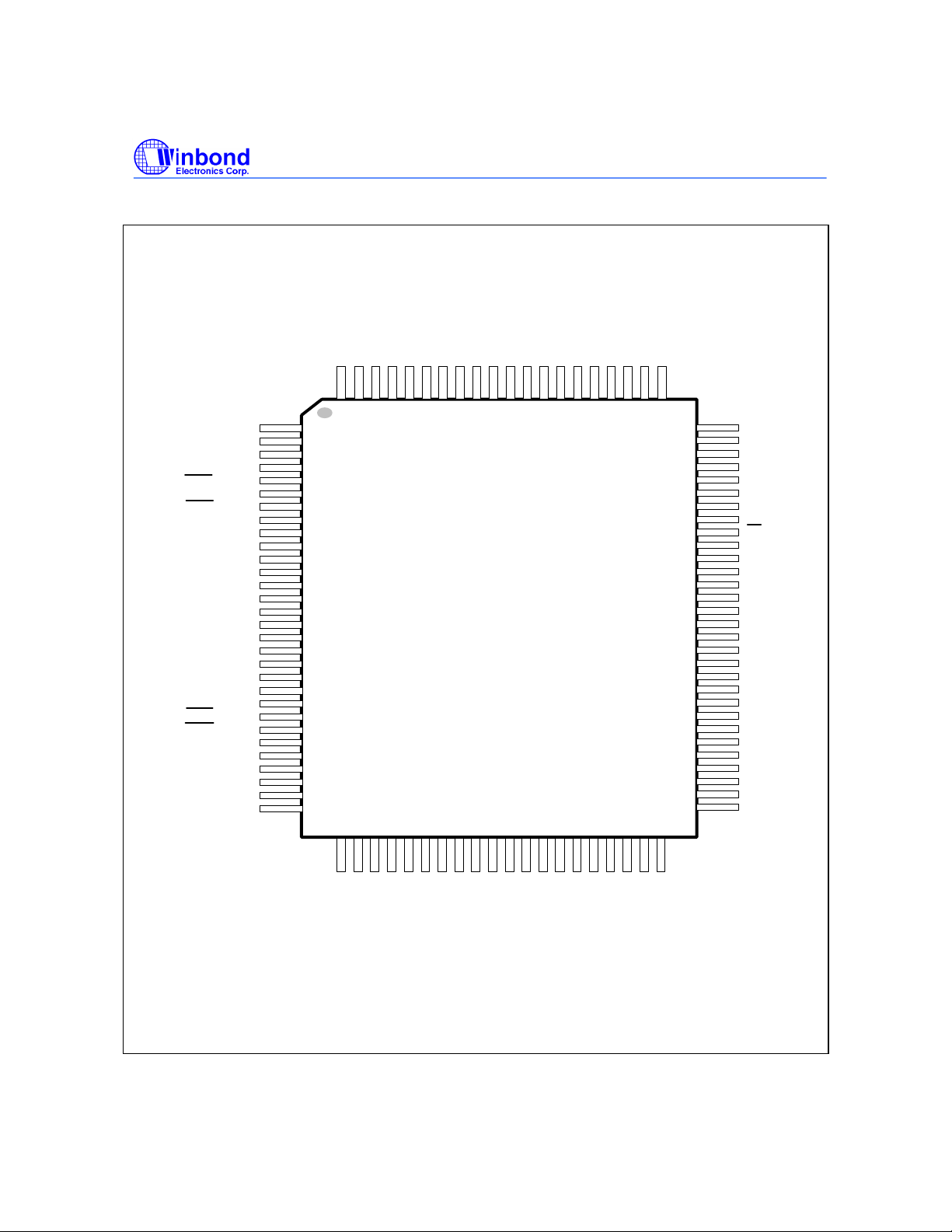
PIN CONFIGURATION
Preliminary W77E468
T
2
,
P
P
P
P
P
P
P
P
5
5
5
5
1
N
.
.
0
.
C
7
6
5
.
.
.
5
4
3
P
5
5
5
.
.
.0D7D6D5D4D3D2D1D
2
1
V
V
D
D
0
D
D
T2EX,P1.1
RXD1,P1.2
TXD1,P1.3
INT2,P1.4
INT3,P1.5
INT4,P1.6
INT5,P1.7
RST
P4.0
P4.1
P4.2
P4.3
P4.4
P4.5
P4.6
P4.7
VDD
VDD
VDD
VDD
RXD,P3.0
TXD,P3.1
INT0,P3.2
INT1,P3.3
T0,P3.4
T1,P3.5
P3.6
P3.7
XTAL2
XTAL1
989
1
1
9
0
2
0
3
4
5
6
7
8
9
10
11
12
13
14
15
16
17
18
19
20
21
22
23
24
25
26
27
28
29
30
31333435363738394
7
3
2
9
9192939495969
0
9
W77E468
100-PIN
QFP
4142434445464748495
0
81828384858687888
80
79
78
77
76
75
74
73
72
71
70
69
68
67
66
65
64
63
62
61
60
59
58
57
56
55
54
53
52
51
0
P0.0
P0.1
P0.2
P0.3
P0.4
P0.5
P0.6
P0.7
EA
VDD
VSS
A0
A1
A2
A3
A4
A5
A6
A7
ALE
NC
VSS
VSS
P2.7
P2.6
P2.5
P2.4
P2.3
P2.2
P2.1
V
V
/
/
/
S
S
R
W
S
S
P
D
R
S
E
N
NCNCP
P
P
P
A
A
A
A
A
A
6
6
6
6
1
1
1
.
.
.
.
3
2
5
1
0
1
4
3
2
A9A8P
1
1
1
0
2
.
0
,
/
W
A
I
T
Publication Release Date: January 1999
- 3 - Revision A1
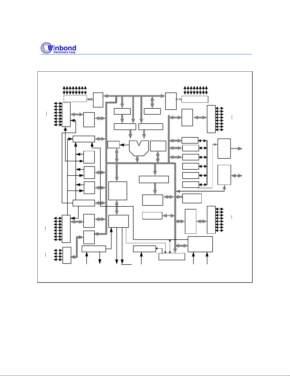
BLOCK DIAGRAM
Preliminary W77E468
P1.0
P1.7
P3.0
P3.7
P6.0
P6.3
P5.0 - P5.7
Port 5
Port
1
Interrupt
2 UARTs
Port
3
Port
6
Port 1
Latch
Timer
2
Timer
0
Timer
1
Port 3
Latch
Port 6
Latch
Oscillator
XTAL1
Port
5
Latch
Port 4
Latch
ACC
PSW
Instruction
Decoder
&
Sequencer
Bus & clock
Controller
ALE GNDV
ALU
Reset Block
PSEN
B
T2 RegisterT1 Register
Stack
Pointer
SFR RAM Address
256 bytes
RAM & SFR
1KB SRAM
Watchdog Timer
RSTXTAL2
P4.0 - P4.7
Port 4
Port 0
Latch
DPTR
DPTR 1
Temp Reg.
PC
Incrementor
Addr. Reg.
32KB ROM
Port 2
Latch
Power control
Power monitor
CC
Addr.
P0.0
P0.7
A0-A15
Port
0
Bus
D0-D7
Data
Bus
Port
2
&
P2.0
P2.7
- 4 -
Preliminary W77E468
EA
PIN DESCRIPTION
SYMBOL TYPE DESCRIPTIONS
I
EXTERNAL ACCESS ENABLE: This pin forces the processor to execute out of
external ROM. It should be kept high to access internal ROM. The ROM
address and data will not be present on the bus if EA pin is high and the
program counter is within 32 KB area. Otherwise they will be present on the
bus.
PSEN
ALE O
RST I L
XTAL1 I
XTAL2 O
VSS I
VDD I
A0−A15
D0−D7
P0.0−P0.7
P1.0−P1.7
O
PROGRAM STORE ENABLE: PSEN pin always emits pulses during access to
internal/external ROM.
ADDRESS LATCH ENABLE: ALE is used to enable the address latch that
separates the address from the data on Port 0.
RESET: A high on this pin for two machine cycles while the oscillator is running
resets the device.
CRYSTAL1: This is the crystal oscillator input. This pin may be driven by an
external clock.
CRYSTAL2: This is the crystal oscillator output. It is the inversion of XTAL1.
GROUND: Ground potential.
POWER SUPPLY: Supply voltage for operation.
O
ADDRESS BUS: This bus dedicates program/data address output during
access to external ROM, on-chip ROM and external RAM.
I
DATA BUS: This bus is used to read/write external memory or peripherals.
I/O
PORT 0: Port 0 is an open-drain bi-directional I/O port.
I/O
PORT 1: Port 1 is a bi-directional I/O port with internal pull-ups. The bits have
alternate functions which are described below:
T2(P1.0): Timer/Counter 2 external count input
T2EX(P1.1): Timer/Counter 2 Reload/Capture/Direction control
RXD1(P1.2): Serial port 2 RXD
TXD1(p1.3): Serial port 2 TXD
INT2(P1.4): External Interrupt 2
P2.0−P2.7
INT3 (P1.5): External Interrupt 3
INT4(P1.6): External Interrupt 4
INT5 (P1.7): External Interrupt 5
I/O
PORT 2: Port 2 is a bi-directional I/O port with internal pull-ups.
Publication Release Date: January 1999
- 5 - Revision A1
Preliminary W77E468
INT
1
WAIT
RD
WR
Pin Description, continued
SYMBOL TYPE DESCRIPTIONS
I/O
P3.0−P3.7
P4.0−P4.7
P5.0−P5.7
P6.0−P6.3
PORT 3: Port 3 is a bi-directional I/O port with internal pull-ups. All bits have
alternate functions, which are described below:
RXD(P3.0) : Serial Port 0 input
TXD(P3.1) : Serial Port 0 output
INT0 (P3.2) : External Interrupt 0
(P3.3) : External Interrupt 1
T0(P3.4) : Timer 0 External Input
T1(P3.5) : Timer 1 External Input
P3.6 : General purpose I/O
P3.7 : General purpose I/O
I/O
PORT 4: functions as a 8-bit bi-directional I/O port but not bit-addressable.
I/O
PORT 5: functions as a 8-bit bi-directional I/O port but not bit-addressable.
I/O
PORT 6: functions as a 4-bit bi-directional I/O port but not bit-addressable. The
P6.0 also provides the alternate function
signal.
which is the wait state control
O
READ STROBE: indicates external data memory read strobe.
O
WRITE STROBE: indicates external data memory write strobe.
* Note: TYPE I: input, O: output, I/O: bi-directional.
FUNCTIONAL DESCRIPTION
The W77E468 is 8052 pin compatible and instruction set compatible. It includes the resources of the
standard 8052 such as four 8-bit I/O Ports, three 16-bit timer/counters, full duplex serial port and
interrupt sources with two priority levels.
The W77E468 features a faster running and better performance 8-bit CPU with a redesigned core
processor without wasted clock and memory cycles. it improves the performance not just by running
at high frequency but also by reducing the machine cycle duration from the standard 8052 period of
twelve clocks to four clock cycles for the majority of instructions. This improves performance by an
average of 1.5 to 3 times. The W77E468 also provides dual Data Pointers (DPTRs) to speed up block
data memory transfers. It can also adjust the duration of the MOVX instruction (access to off-chip
data memory) between two machine cycles and nine machine cycles. This flexibility allows the
W77E468 to work efficiently with both fast and slow RAMs and peripheral devices. In addition, the
W77E468 contains on-chip 1KB MOVX SRAM, the address of which is between 0000H and 03FFH. It
only can be accessed by MOVX instruction; this on-chip SRAM is optional under software control.
- 6 -

Preliminary W77E468
The W77E468 is an 8052 compatible device that gives the user the features of the original 8052
device, but with improved speed and power consumption characteristics. It has the same instruction
set as the 8051 family, with one addition: DEC DPTR (op-code A5H, the DPTR is decreased by 1).
While the original 8051 family was designed to operate at 12 clock periods per machine cycle, the
W77E468 operates at a much reduced clock rate of only 4 clock periods per machine cycle. This
naturally speeds up the execution of instructions. Consequently, the W77E468 can run at a higher
speed as compared to the original 8052, even if the same crystal is used. Since the W77E468 is a
fully static CMOS design, it can also be operated at a lower crystal clock, giving the same throughput
in terms of instruction execution, yet reducing the power consumption.
The 4 clocks per machine cycle feature in the W77E468 is responsible for a three-fold increase in
execution speed. The W77E468 has all the standard features of the 8052, and has a few extra
peripherals and features as well.
Seven I/O Ports:
The W77E468 has six 8-bit I/O ports and one 4-bit I/O port, giving a total of 52 lines. Port 0 to Port 3
can be used as a 8-bit general I/O port with bit-addressable. Port 4 and Port 5 are 8-bit general I/O
port without bit-addressable. Port 6 is a 4-bit general I/O port without bit-addressable. Port 1 to Port 5
have internal pull-up, Port 0 is open-drain.
Serial I/O:
The W77E468 has two enhanced serial ports that are functionally similar to the serial port of the
original 8052 family. However the serial ports on the W77E468 can operate in different modes in
order to obtain timing similarity as well. Note that the serial port 0 can use Timer 1 or 2 as baud rate
generator, but the serial port 1 can only use Timer 1 as baud rate generator. The serial ports have the
enhanced features of Automatic Address recognition and Frame Error detection.
Timers:
The W77E468 has three 16-bit timers that are functionally similar to the timers of the 8052 family.
When used as timers, they can be set to run at either 4 clocks or 12 clocks per count, thus providing
the user with the option of operating in a mode that emulates the timing of the original 8052. The
W77E468 has an additional feature, the watchdog timer. This timer is used as a System Monitor or as
a very long time period timer.
Interrupts:
The Interrupt structure in the W77E468 is slightly different from that of the standard 8052. Due to the
presence of additional features and peripherals, the number of interrupt sources and vectors has been
increased. The W77E468 provides 12 interrupt resources with two priority level, including six external
interrupt sources, timer interrupts, serial I/O interrupts and power-fail interrupt.
Publication Release Date: January 1999
- 7 - Revision A1

Preliminary W77E468
Data Pointers:
The original 8052 had only one 16-bit Data Pointer (DPL, DPH). In the W77E468, there is an
additional 16-bit Data Pointer (DPL1, DPH1). This new Data Pointer uses two SFR locations which
were unused in the original 8052. In addition there is an added instruction, DEC DPTR (op-code
A5H), which helps in improving programming flexibility for the user.
Power Management:
Like the standard 80C52, the W77E468 also has IDLE and POWER DOWN modes of operation. The
W77E468 provides a new Economy mode which allow user to switch the internal clock rate divided by
either 4, 64 or 1024. In the IDLE mode, the clock to the CPU core is stopped while the timers, serial
ports and interrupts clock continue to operate. In the POWER DOWN mode, all the clock are stopped
and the chip operation is completely stopped. This is the lowest power consumption state.
On-chip Data SRAM:
The W77E468 has 1K Bytes of data space SRAM which is read/write accessible and is memory
mapped. This on-chip MOVX SRAM is reached by the MOVX instruction. It is not used for executable
program memory. There is no conflict or overlap among the 256 bytes Scratchpad RAM and the 1K
Bytes MOVX SRAM as they use different addressing modes and separate instructions. The on-chip
MOVX SRAM is enabled by setting the DME0 bit in the PMR register. After a reset, the DME0 bit is
cleared such that the on-chip MOVX SRAM is disabled, and all data memory spaces 0000H−FFFFH
access to the external memory.
MEMORY ORGANIZATION
The W77E468 separates the memory into two separate sections, the Program Memory and the Data
Memory. The Program Memory is used to store the instruction op-codes, while the Data Memory is
used to store data or for memory mapped devices.
Program Memory:
The Program Memory on the W77E468 can be up to 64Kbytes long. There is also on-chip ROM
which can be used similarly to that of the 8052, except that the ROM size is 32Kbytes. All
instructions are fetched for execution from this memory area. The MOVC instruction can also access
this memory region. Exceeding the maximum address of on-chip ROM will access to the external
memory.
- 8 -

Preliminary W77E468
Data Memory:
The W77E468 can access up to 64Kbytes of external Data Memory. This memory region is accessed
by the MOVX instructions. Unlike the 8051 derivatives, the W77E468 contains on-chip 1K bytes
MOVX SRAM of Data Memory, which can only be accessed by MOVX instructions. These 1K bytes of
SRAM are between address 0000H and 03FFH. Access to the on-chip MOVX SRAM is optional under
software control. When enabled by software, any MOVX instruction that uses this area will go to the
on-chip RAM. MOVX addresses greater than 03FFH automatically go to external memory through
Port 0 and 2. When disabled, the 1KB memory area is transparent to the system memory map. Any
MOVX directed to the space between 0000H and FFFFH goes to the expanded bus on A0-A15 and
D0-D7. This is the default condition. In addition, the W77E468 has the standard 256 bytes of on-chip
Scratchpad RAM. This can be accessed either by direct addressing or by indirect addressing. There
are also some Special Function Registers (SFRs), which can only be accessed by direct addressing.
Since the Scratchpad RAM is only 256 bytes, it can be used only when data contents are small. In the
event that larger data contents are present, two selections can be used. One is on-chip MOVX SRAM
, the other is the external Data Memory. The on-chip MOVX SRAM can only be accessed by a MOVX
instruction, the same as that for external Data Memory. However, the on-chip RAM has the fastest
access times.
FFh
80h
7Fh
00h
Indirect
Addressing
RAM
Direct &
Indirect
Addressing
RAM
SFRs
Direct
Addressing
03FFh
0000h
only
1K Bytes
On-chip SRAM
FFFFh
0000h
Figure 1. Memory Map
64 K
Bytes
External
Data
Memory
FFFFh
External
Program
Memory
7FFFh
32K Bytes
On-chip
Program
Memory
0000h
Publication Release Date: January 1999
- 9 - Revision A1
FFh
80h
7Fh
30h
2Fh
2Eh
2Dh
2Ch
2Bh
2Ah
29h
28h
27h
26h
25h
24h
23h
22h
21h
20h
1Fh
18h
17h
10h
0Fh
08h
07h
00h
Indirect RAM
Direct RAM
5D5E5F
555657
Bank 3
Bank 2
Bank 1
Bank 0
Preliminary W77E468
78797A7B7C7D7E7F
7071727374757677
68696A6B6C6D6E6F
6061626364656667
58595A5B5C
5051525354
48494A4B4C4D4E4F
4041424344454647
Bit Addressable
38393A3B3C3D3E3F
20H-2FH
3031323334353637
28292A2B2C2D2E2F
2021222324252627
18191A1B1C1D1E1F
1011121314151617
08090A0B0C0D0E0F
0001020304050607
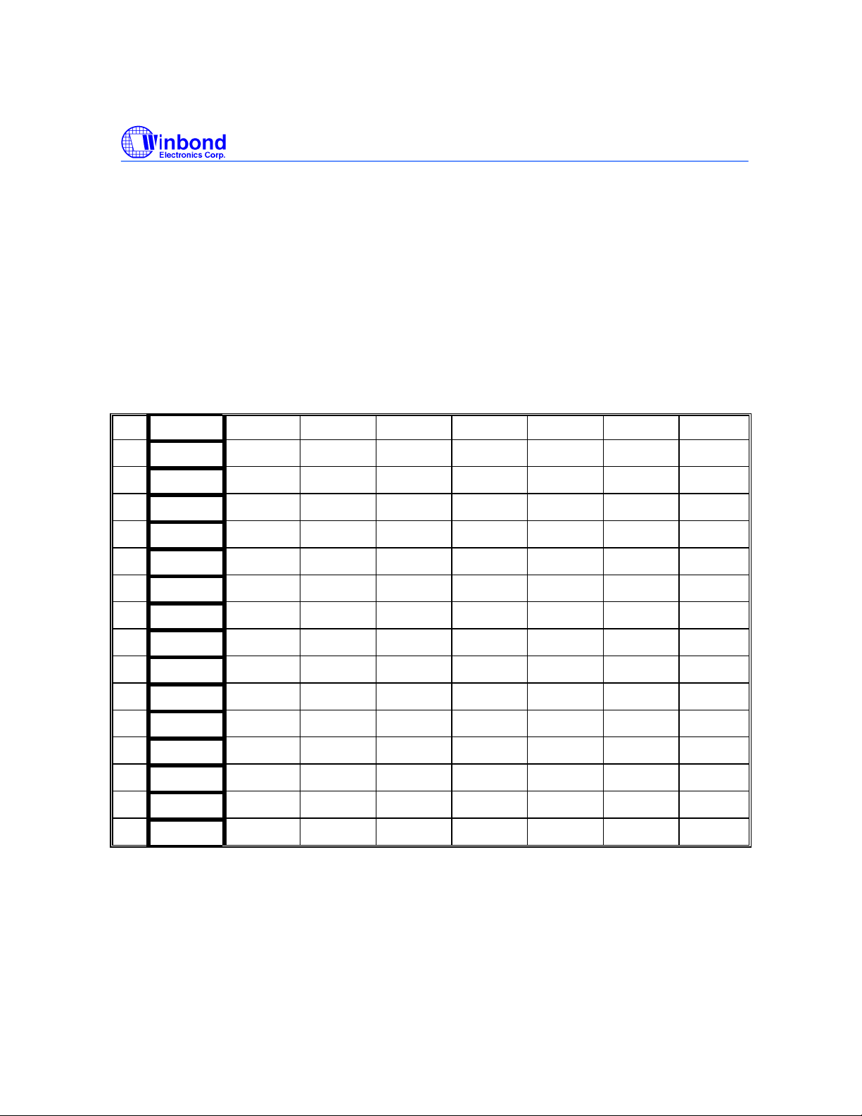
Figure 2. Scratchpad RAM/Register Addressing
- 10 -
Preliminary W77E468
Special Function Registers
The W77E468 uses Special Function Registers (SFRs) to control and monitor peripherals and their
Modes.
The SFRs reside in the register locations 80-FFh and are accessed by direct addressing only. Some
of the SFRs are bit addressable. This is very useful in cases where one wishes to modify a particular
bit without changing the others. The SFRs that are bit addressable are those whose addresses end in
0 or 8. The W77E468 contains all the SFRs present in the standard 8052. However, some additional
SFRs have been added. In some cases unused bits in the original 8052 have been given new
functions. The list of SFRs is as follows. The table is condensed with eight locations per row. Empty
locations indicate that there are no registers at these addresses. When a bit or register is not
implemented, it will read high.
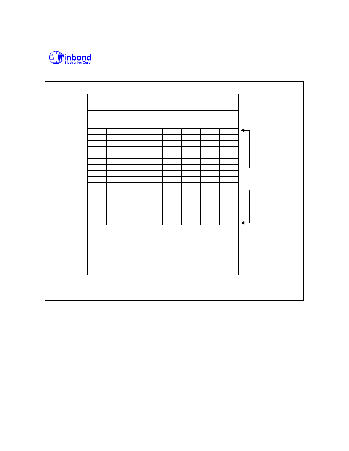
Table 1. Special Function Register Location Table
F8 EIP
F0 B
E8 EIE
E0 ACC
D8 WDCON
D0 PSW
C8 T2CON T2MOD RCAP2L RCAP2H TL2 TH2
C0 SCON1 SBUF1 ROMMAP PMR STATUS TA
B8 IP SADEN SADEN1
B0 P3
A8 IE SADDR SADDR1
A0 P2 HB P6 P4 P5
98 SCON0 SBUF
90 P1 EXIF
88 TCON TMOD TL0 TL1 TH0 TH1 CKCON
80 P0 SP DPL DPH DPL1 DPH1 DPS PCON
Note: The SFRs in the column with dark borders are bit-addressable.
Publication Release Date: January 1999
- 11 - Revision A1

Preliminary W77E468
A brief description of the SFRs now follows.
PORT 0
Bit: 7 6 5 4 3 2 1 0
P0.7 P0.6 P0.5 P0.4 P0.3 P0.2 P0.1 P0.0
Mnemonic: P0 Address: 80h
Port 0 is an open-drain bi-directional I/O port.
STACK POINTER
Bit: 7 6 5 4 3 2 1 0
SP.7 SP.6 SP.5 SP.4 SP.3 SP.2 SP.1 SP.0
Mnemonic: SP Address: 81h
The Stack Pointer stores the Scratchpad RAM address where the stack begins. In other words, it
always points to the top of the stack.
DATA POINTER LOW
Bit: 7 6 5 4 3 2 1 0
DPL.7 DPL.6 DPL.5 DPL.4 DPL.3 DPL.2 DPL.1 DPL.0
Mnemonic: DPL Address: 82h
This is the low byte of the standard 8052 16-bit data pointer.
DATA POINTER HIGH
Bit: 7 6 5 4 3 2 1 0
DPH.7 DPH.6 DPH.5 DPH.4 DPH.3 DPH.2 DPH.1 DPH.0
Mnemonic: DPH Address: 83h
This is the high byte of the standard 8052 16-bit data pointer.
DATA POINTER LOW1
Bit: 7 6 5 4 3 2 1 0
DPL1.7 DPL1.6 DPL1.5 DPL1.4 DPL1.3 DPL1.2 DPL1.1 DPL1.0
Mnemonic: DPL1 Address: 84h
- 12 -

Preliminary W77E468
This is the low byte of the new additional 16-bit data pointer that has been added to the W77E468.
The user can switch between DPL, DPH and DPL1, DPH1 simply by setting register DPS = 1. The
instructions that use DPTR will now access DPL1 and DPH1 in place of DPL and DPH. If they are not
required they can be used as conventional register locations by the user.
DATA POINTER HIGH1
Bit: 7 6 5 4 3 2 1 0
DPH1.7 DPH1.6 DPH1.5 DPH1.4 DPH1.3 DPH1.2 DPH1.1 DPH1.0
Mnemonic: DPH1 Address: 85h
This is the high byte of the new additional 16-bit data pointer that has been added to the W77E468.
The user can switch between DPL, DPH and DPL1, DPH1 simply by setting register DPS = 1. The
instructions that use DPTR will now access DPL1 and DPH1 in place of DPL and DPH. If they are not
required they can be used as conventional register locations by the user.
DATA POINTER SELECT
Bit: 7 6 5 4 3 2 1 0
- - - - - - - DPS.0
Mnemonic: DPS Address: 86h
DPS.0: This bit is used to select either the DPL,DPH pair or the DPL1,DPH1 pair as the active Data
Pointer. When set to 1, DPL1,DPH1 will be selected, otherwise DPL,DPH will be selected.
DPS.1-7:These bits are reserved, but will read 0.
POWER CONTROL
Bit: 7 6 5 4 3 2 1 0
SM0D
Mnemonic: PCON Address: 87h
SMOD : This bit doubles the serial port baud rate in mode 1, 2, and 3 when set to 1.
SMOD0: Framing Error Detection Enable: When SMOD0 is set to 1, then SCON.7(SCON1.7)
indicates a Frame Error and acts as the FE(FE_1) flag. When SMOD0 is 0, then
SCON.7(SCON1.7) acts as per the standard 8052 function.
GF1-0: These two bits are general purpose user flags.
PD: Setting this bit causes the W77E468 to go into the POWER DOWN mode. In this mode all
the clocks are stopped and program execution is frozen.
IDL: Setting this bit causes the W77E468 to go into the IDLE mode. In this mode the clocks to the
CPU are stopped, so program execution is frozen. But the clock to the serial, timer and
interrupt blocks is not stopped, and these blocks continue operating.
SMOD0
- - GF1 GF0 PD IDL
Publication Release Date: January 1999
- 13 - Revision A1
Preliminary W77E468
INT
1
T
T
INTx
TIMER CONTROL
Bit: 7 6 5 4 3 2 1 0
TF1 TR1 TF0 TR0 IE1 IT1 IE0 IT0
Mnemonic: TCON Address: 88h
TF1: Timer 1 overflow flag: This bit is set when Timer 1 overflows. It is cleared automatically when
the program does a timer 1 interrupt service routine. Software can also set or clear this bit.
TR1: Timer 1 run control: This bit is set or cleared by software to turn timer/counter on or off.
TF0: Timer 0 overflow flag: This bit is set when Timer 0 overflows. It is cleared automatically when
the program does a timer 0 interrupt service routine. Software can also set or clear this bit.
TR0: Timer 0 run control: This bit is set or cleared by software to turn timer/counter on or off.
IE1: Interrupt 1 edge detect: Set by hardware when an edge/level is detected on
cleared by hardware when the service routine is vectored to only if the interrupt was edge
triggered. Otherwise it follows the pin.
IT1: Interrupt 1 type control: Set/cleared by software to specify falling edge/ low level triggered
external inputs.
IE0: Interrupt 0 edge detect: Set by hardware when an edge/level is detected on INT0 . This bit is
cleared by hardware when the service routine is vectored to only if the interrupt was edge
triggered. Otherwise it follows the pin.
IT0: Interrupt 0 type control: Set/cleared by software to specify falling edge/ low level triggered
external inputs.
TIMER MODE CONTROL
Bit: 7 6 5 4 3 2 1 0
GATE
Mnemonic: TMOD Address: 89h
GATE: Gating control: When this bit is set, Timer/counter x is enabled only while
and TRx control bit is set. When cleared, Timer x is enabled whenever TRx control bit is set.
C/T: Timer or Counter Select: When cleared, the timer is incremented by internal clocks. When
set, the timer counts high-to-low edges of the Tx pin.
C/
TIMER1 TIMER0
M1 M0 GATE
C/
. This bit is
M1 M0
pin is high
- 14 -

Preliminary W77E468
M1, M0: Mode Select bits:
M1 M0 Mode
0 0 Mode 0: 8-bits with 5-bit prescale.
0 1 Mode 1: 18-bits, no prescale.
1 0 Mode 2: 8-bits with auto-reload from Thx
1 1 Mode 3: (Timer 0) TL0 is an 8-bit timer/counter controlled by the
standard Timer 0 control bits. TH0 is a 8-bit timer only controlled by Timer 1
control bits. (Timer 1) Timer/counter is stopped.
TIMER 0 LSB
Bit: 7 6 5 4 3 2 1 0
TL0.7 TL0.6 TL0.5 TL0.4 TL0.3 TL0.2 TL0.1 TL0.0
Mnemonic: TL0 Address: 8Ah
TL0.7-0:Timer 0 LSB
TIMER 1 LSB
Bit: 7 6 5 4 3 2 1 0
Mnemonic: TL1 Address: 8Bh
TL1.7-0:Timer 1 LSB
TIMER 0 MSB
Bit: 7 6 5 4 3 2 1 0
Mnemonic: TH0 Address: 8Ch
TH0.7-0:Timer 0 MSB
TIMER 1 MSB
Bit: 7 6 5 4 3 2 1 0
Mnemonic: TH1 Address: 8Dh
TH1.7-0:Timer 1 MSB
TL1.7 TL1.6 TL1.5 TL1.4 TL1.3 TL1.2 TL1.1 TL1.0
TH0.7 TH0.6 TH0.5 TH0.4 TH0.3 TH0.2 TH0.1 TH0.0
TH1.7 TH1.6 TH1.5 TH1.4 TH1.3 TH1.2 TH1.1 TH1.0
Publication Release Date: January 1999
- 15 - Revision A1

Preliminary W77E468
17
20
23
26
WR
CLOCK CONTROL
Bit: 7 6 5 4 3 2 1 0
WD1 WD0 T2M T1M T0M MD2 MD1 MD0
Mnemonic: CKCON Address: 8Eh
WD1-0:Watchdog timer mode select bits: These bits determine the time-out period for the watchdog
timer. In all four time-out options the reset time-out is 512 clocks more than the interrupt time-
out period.
WD1 WD0 Interrupt time-out Reset time-out
0 0
0 1
1 0
1 1
T2M: Timer 2 clock select: When T2M is set to 1, timer 2 uses a divide by 4 clock, and when set to
0 it uses a divide by 12 clock.
T1M: Timer 1 clock select: When T1M is set to 1, timer 1 uses a divide by 4 clock, and when set to
0 it uses a divide by 12 clock.
T0M: Timer 0 clock select: When T0M is set to 1, timer 0 uses a divide by 4 clock, and when set to
0 it uses a divide by 12 clock.
MD2-0: Stretch MOVX select bits: These three bits are used to select the stretch value for the MOVX
instruction. Using a variable MOVX length enables the user to access slower external memory
devices or peripherals without the need for external circuits. The RD or
stretched by the selected interval. When accessing the on-chip SRAM, the MOVX instruction
is always in 2 machine cycles regardless of the stretch setting. By default, the stretch has
value of 1. If the user needs faster accessing, then a stretch value of 0 should be selected.
MD2 MD1 MD0 Stretch value MOVX duration
0 0 0 0 2 machine cycles
0 0 1 1 3 machine cycles (Default)
0 1 0 2 4 machine cycles
0 1 1 3 5 machine cycles
1 0 0 4 6 machine cycles
1 0 1 5 7 machine cycles
1 1 0 6 8 machine cycles
1 1 1 7 9 machine cycles
2
2
2
2
217 + 512
220 + 512
223 + 512
226 + 512
strobe will be
- 16 -

Preliminary W77E468
PORT 1
Bit: 7 6 5 4 3 2 1 0
P1.7 P1.6 P1.5 P1.4 P1.3 P1.2 P1.1 P1.0
Mnemonic: P1 Address: 90h
P1.7-0: General purpose I/O port. Most instructions will read the port pins in case of a port read
access, however in case of read-modify-write instructions, the port latch is read. Some pins
also have alternate input or output functions. This alternate functions are described below:
P1.0 : T2 External I/O for Timer/Counter 2
P1.1 : T2EX Timer/Counter 2 Capture/Reload Trigger
P1.2 : RXD1 Serial Port 1 Receive
P1.3 : TXD1 Serial Port 1 Transmit
P1.4 : INT2 External Interrupt 2
P1.5 : INT3
P1.6 : INT4 External Interrupt 4
P1.7 : INT5
External Interrupt 3
External Interrupt 5
EXTERNAL INTERRUPT FLAG
Bit: 7 6 5 4 3 2 1 0
IE5 IE4 IE3 IE2
Mnemonic: EXIF Address: 91h
IE5: External Interrupt 5 flag. Set by hardware when a falling edge is detected on INT5 .
IE4: External Interrupt 4 flag. Set by hardware when a rising edge is detected on INT4.
IE3: External Interrupt 3 flag. Set by hardware when a falling edge is detected on INT3 .
IE2: External Interrupt 2 flag. Set by hardware when a rising edge is detected on INT2.
XT/RG : Crystal/RC Oscillator Select. Setting this bit selects crystal or external clock as system clock
source. Clearing this bit selects the on-chip RC oscillator as clock source. XTUP(STATUS.4)
must be set to 1 and XTOFF (PMR.3) must be cleared before this bit can be set. Attempts to
set this bit without obeying these conditions will be ignored. This bit is set to 1 after a poweron reset and unchanged by other forms of reset.
RGMD: RC Mode Status. This bit indicates the current clock source of microcontroller. When cleared,
CPU is operating from the external crystal or oscillator. When set, CPU is operating from the
on-chip RC oscillator. This bit is cleared to 0 after a power-on reset and unchanged by other
forms of reset.
XT/RG
RGMD RGSL -
Publication Release Date: January 1999
- 17 - Revision A1

Preliminary W77E468
RGSL: RC Oscillator Select. This bit selects the clock source following a resume from Power Down
Mode. Setting this bit allows device operating from RC oscillator when a resume from Power
Down Mode. When this bit is cleared, the device will hold operation until the crystal oscillator
has warmed-up following a resume from Power Down Mode. This bit is cleared to 0 after a
power-on reset and unchanged by other forms of reset.
SERIAL PORT CONTROL
Bit: 7 6 5 4 3 2 1 0
SM0/FE SM1 SM2 REN TB8 RB8 TI RI
Mnemonic: SCON Address: 98h
SM0/FE: Serial port 0, Mode 0 bit or Framing Error Flag: The SMOD0 bit in PCON SFR determines
whether this bit acts as SM0 or as FE. The operation of SM0 is described below. When used
as FE, this bit will be set to indicate an invalid stop bit. This bit must be manually cleared in
software to clear the FE condition.
SM1: Serial port Mode bit 1:
SM0 SM1 Mode Description Length Baud rate
0 0 0 Synchronous 8 4/12 Tclk
0 1 1 Asynchronous 10 variable
1 0 2 Asynchronous 11 64/32 Tclk
1 1 3 Asynchronous 11 variable
SM2: Multiple processors communication. Setting this bit to 1 enables the multiprocessor
communication feature in mode 2 and 3. In mode 2 or 3, if SM2 is set to 1, then RI will not be
activated if the received 9th data bit (RB8) is 0. In mode 1, if SM2 = 1, then RI will not be
activated if a valid stop bit was not received. In mode 0, the SM2 bit controls the serial port
clock. If set to 0, then the serial port runs at a divide by 12 clock of the oscillator. This gives
compatibility with the standard 8052. When set to 1, the serial clock become divide by 4 of
the oscillator clock. This results in faster synchronous serial communication.
REN: Receive enable: When set to 1 serial reception is enabled, otherwise reception is disabled.
TB8: This is the 9th bit to be transmitted in modes 2 and 3. This bit is set and cleared by software
as desired.
RB8: In modes 2 and 3 this is the received 9th data bit. In mode 1, if SM2 = 0, RB8 is the stop bit
that was received. In mode 0 it has no function.
TI: Transmit interrupt flag: This flag is set by hardware at the end of the 8th bit time in mode 0, or
at the beginning of the stop bit in all other modes during serial transmission. This bit must be
cleared by software.
- 18 -

Preliminary W77E468
RI: Receive interrupt flag: This flag is set by hardware at the end of the 8th bit time in mode 0, or
halfway through the stop bits time in the other modes during serial reception. However the
restrictions of SM2 apply to this bit. This bit can be cleared only by software.
SERIAL DATA BUFFER
Bit: 7 6 5 4 3 2 1 0
SBUF.7 SBUF.6 SBUF.5 SBUF.4 SBUF.3 SBUF.2 SBUF.1 SBUF.0
Mnemonic: SBUF Address: 99h
SBUF.7-0: Serial data on the serial port 0 is read from or written to this location. It actually consists of
two separate internal 8-bit registers. One is the receive resister, and the other is the
transmit buffer. Any read access gets data from the receive data buffer, while write access
is to the transmit data buffer.
PORT 2
Bit: 7 6 5 4 3 2 1 0
P2.7 P2.6 P2.5 P2.4 P2.3 P2.2 P2.1 P2.0
Mnemonic: P2 Address: A0h
P2.7-0: Port 2 is a bi-directional I/O port with internal pull-ups.
HIGH BYTE REGISTER
Bit: 7 6 5 4 3 2 1 0
Mnemonic: HB Address: A1h
This register contains the high byte address during execution of " MOVX @Ri, " instructions.
PORT 4
Bit: 7 6 5 4 3 2 1 0
P4.7 P4.6 P4.5 P4.4 P4.3 P4.2 P4.1 P4.0
Mnemonic: P4 Address: A6h
P4.7-0: Port 4 is a bi-directional I/O port with internal pull-ups.
Publication Release Date: January 1999
- 19 - Revision A1

Preliminary W77E468
PORT 5
Bit: 7 6 5 4 3 2 1 0
P5.7 P5.6 P5.5 P5.4 P5.3 P5.2 P5.1 P5.0
Mnemonic: P5 Address: A7h
P5.7-0: Port 5 is a bi-directional I/O port with internal pull-ups.
PORT 6
Bit: 7 6 5 4 3 2 1 0
- - - - P6.3 P6.2 P6.1 P6.0
Mnemonic: P6 Address: A5h
P6.3-0: Port 6 is a 4-bit bi-directional I/O port with internal pull-ups.
INTERRUPT ENABLE
Bit: 7 6 5 4 3 2 1 0
EA ES1 ET2 ES ET1 EX1 ET0 EX0
Mnemonic: IE Address: A8h
EA: Global enable. Enable/disable all interrupts except for PFI.
ES1: Enable Serial Port 1 interrupt.
ET2: Enable Timer 2 interrupt.
ES: Enable Serial Port 0 interrupt.
ET1: Enable Timer 1 interrupt
EX1: Enable external interrupt 1
ET0: Enable Timer 0 interrupt
EX0: Enable external interrupt 0
SLAVE ADDRESS
Bit: 7 6 5 4 3 2 1 0
Mnemonic: SADDR Address: A9h
SADDR: The SADDR should be programmed to the given or broadcast address for serial port 0 to
which the slave processor is designated.
- 20 -

Preliminary W77E468
INT
1
SLAVE ADDRESS 1
Bit: 7 6 5 4 3 2 1 0
Mnemonic: SADDR1 Address: AAh
SADDR1: The SADDR1 should be programmed to the given or broadcast address for serial port 1 to
which the slave processor is designated.
PORT 3
Bit: 7 6 5 4 3 2 1 0
- - P3.5 P3.4 P3.3 P3.2 P3.1 P3.0
Mnemonic: P3 Address: B0h
P3.5-0: General purpose I/O port. Each pin also has an alternate input or output function. The
alternate
functions are described below.
P3.5 T1 Timer/counter 1 external count input
P3.4 T0 Timer/counter 0 external count input
P3.3
P3.2 INT0 External interrupt 0
P3.1 TxD Serial port 0 output
P3.0 RxD Serial port 0 input
INTERRUPT PRIORITY
Bit: 7 6 5 4 3 2 1 0
Mnemonic: IP Address: B8h
IP.7: This bit is un-implemented and will read high.
PS1: This bit defines the Serial port 1 interrupt priority. PS = 1 sets it to higher priority level.
PT2: This bit defines the Timer 2 interrupt priority. PT2 = 1 sets it to higher priority level.
PS: This bit defines the Serial port 0 interrupt priority. PS = 1 sets it to higher priority level.
PT1: This bit defines the Timer 1 interrupt priority. PT1 = 1 sets it to higher priority level.
PX1: This bit defines the External interrupt 1 priority. PX1 = 1 sets it to higher priority level.
PT0: This bit defines the Timer 0 interrupt priority. PT0 = 1 sets it to higher priority level.
PX0: This bit defines the External interrupt 0 priority. PX0 = 1 sets it to higher priority level.
External interrupt 1
- PS1 PT2 PS PT1 PX1 PT0 PX0
Publication Release Date: January 1999
- 21 - Revision A1

Preliminary W77E468
SLAVE ADDRESS MASK ENABLE
Bit: 7 6 5 4 3 2 1 0
Mnemonic: SADEN Address: B9h
SADEN: This register enables the Automatic Address Recognition feature of the Serial port 0. When
a bit in the SADEN is set to 1, the same bit location in SADDR will be compared with the
incoming serial data. When SADEN.n is 0, then the bit becomes a "don't care" in the
comparison. This register enables the Automatic Address Recognition feature of the Serial
port 0. When all the bits of SADEN are 0, interrupt will occur for any incoming address.
SLAVE ADDRESS MASK ENABLE 1
Bit: 7 6 5 4 3 2 1 0
Mnemonic: SADEN1 Address: BAh
SADEN1:This register enables the Automatic Address Recognition feature of the Serial port 1. When
a bit in the SADEN1 is set to 1, the same bit location in SADDR1 will be compared with the
incoming serial data. When SADEN1.n is 0, then the bit becomes a "don't care" in the
comparison. This register enables the Automatic Address Recognition feature of the Serial
port 1. When all the bits of SADEN1 are 0, interrupt will occur for any incoming address.
SERIAL PORT CONTROL 1
Bit: 7 6 5 4 3 2 1 0
SM0_1/FE_1 SM1_1 SM2_1 REN_1 TB8_1 RB8_1 TI_1 RI_1
Mnemonic: SCON1 Address: C0h
SM0_1/FE_1: Serial port 1, Mode 0 bit or Framing Error Flag 1: The SMOD0 bit in PCON SFR
determines whether this bit acts as SM0_1 or as FE_1. the operation of SM0_1 is
described below. When used as FE_1, this bit will be set to indicate an invalid stop bit.
This bit must be manually cleared in software to clear the FE_1 condition.
SM1_1:Serial port 1 Mode bit 1:
SM0_1 SM1_1 Mode Description Length Baud rate
0 0 0 Synchronous 8 4/12 Tclk
0 1 1 Asynchronous 10 variable
1 0 2 Asynchronous 11 64/32 Tclk
1 1 3 Asynchronous 11 variable
- 22 -

Preliminary W77E468
WAIT
WAIT
SM2_1:Multiple processors communication. Setting this bit to 1 enables the multiprocessor
communication feature in mode 2 and 3. In mode 2 or 3, if SM2_1 is set to 1, then RI_1 will
not be activated if the received 9th data bit (RB8_1) is 0. In mode 1, if SM2_1 = 1, then RI_1
will not be activated if a valid stop bit was not received. In mode 0, the SM2_1 bit controls the
serial port 1 clock. If set to 0, then the serial port 1 runs at a divide by 12 clock of the
oscillator. This gives compatibility with the standard 8052. When set to 1, the serial clock
become divide by 4 of the oscillator clock. This results in faster synchronous serial
communication.
REN_1:Receive enable: When set to 1 serial reception is enabled, otherwise reception is disabled.
TB8_1: This is the 9th bit to be transmitted in modes 2 and 3. This bit is set and cleared by software
as desired.
RB8_1: In modes 2 and 3 this is the received 9th data bit. In mode 1, if SM2_1 = 0, RB8_1 is the stop
bit that was received. In mode 0 it has no function.
TI_1: Transmit interrupt flag: This flag is set by hardware at the end of the 8th bit time in mode 0, or
at the beginning of the stop bit in all other modes during serial transmission. This bit must be
cleared by software.
RI_1: Receive interrupt flag: This flag is set by hardware at the end of the 8th bit time in mode 0, or
halfway through the stop bits time in the other modes during serial reception. However the
restrictions of SM2_1 apply to this bit. This bit can be cleared only by software.
SERIAL DATA BUFFER 1
Bit: 7 6 5 4 3 2 1 0
SBUF1.7 SBUF1.6 SBUF1.5 SBUF1.4 SBUF1.3 SBUF1.2 SBUF1.1 SBUF1.0
Mnemonic: SBUF1 Address: C1h
SBUF1.7-0: Serial data of the serial port 1 is read from or written to this location. It actually consists
of two separate 8-bit registers. One is the receive resister, and the other is the transmit
buffer. Any read access gets data from the receive data buffer, while write accesses are
to the transmit data buffer.
ROMMAP
Bit: 7 6 5 4 3 2 1 0
WS 1 - - - - - -
Mnemonic: ROMMAP Address: C2h
WS: Wait State Signal Enable. Setting this bit enables the
device will sample the wait state control signal
instruction. This bit is time access protected.
signal on P6.0. The
via P6.0 during MOVX
Publication Release Date: January 1999
- 23 - Revision A1

Preliminary W77E468
POWER MANAGEMENT REGISTER
Bit: 7 6 5 4 3 2 1 0
CD1 CD0 SWB - XTOFF
Mnemonic: PMR Address: C4h
CD1,CD0: Clock Divide Control. These bit selects the number of clocks required to generate one
machine cycle. There are three modes including divide by 4, 64 or 1024. Switching between
modes must first go back devide by 4 mode. For instance, to go from 64 to 1024
clocks/machine cycle the device must first go from 64 to 4 clocks/machine cycle, and then
from 4 to 1024 clocks/machine cycle.
CD1, CD0 clocks/machine cycle
0 0 Reserved
0 1 4
1 0 64
1 1 1024
SWB: Switchback Enable. Setting this bit allows an enabled external interrupt or serial port activity
to force the CD1,CD0 to divide by 4 state (0,1). The device will switch modes at the start of
the jump to interrupt service routine while a external interrupt is enabled and actually
recongnized by microcontroller. While a serial port reception, the switchback occurs at the
start of the instruction following the falling edge of the start bit.
XTOFF: Crystal Oscillator Disable. Setting this bit disables the external crystal oscillator. This bit can
only be set to 1 while the microcontroller is operating from the RC oscillator. Clearing this bit
restarts the crystal oscillator, the XTUP (STATUS.4) bit will be set after crystal oscillator
warmed-up has completed.
ALEOFF: This bit disables the expression of the ALE signal on the device pin during all on-board
program and data memory accesses. External memory accesses will automatically enable
ALE independent of ALEOFF.
0 = ALE expression is enable; 1 = ALE expression is disable
DME0: This bit determines the on-chip MOVX SRAM to be enabled or disabled. Set this bit to 1 will
enable the on-chip 1KB MOVX SRAM.
ALE-OFF
- DME0
- 24 -

Preliminary W77E468
STATUS REGISTER
Bit: 7 6 5 4 3 2 1 0
- HIP LIP XTUP SPTA1 SPRA1 SPTA0 SPRA0
Mnemonic: STATUS Address: C5h
HIP: High Priority Interrupt Status. When set, it indicates that software is servicing a high priority
interrupt. This bit will be cleared when the program executes the corresponding RETI
instruction.
LIP: Low Priority Interrupt Status. When set, it indicates that software is servicing a low priority
interrupt. This bit will be cleared when the program executes the corresponding RETI
instruction.
XTUP:Crystal Oscillator Warm-up Status. when set, this bit indicates the crystal oscillator has
completed the 65536 clocks warm-up delay. Each time the crystal oscillator is restarted by exit
from power down mode or the XTOFF bit is set, hardware will clear this bit. This bit is set to 1
after a power-on reset. When this bit is cleared, it prevents software from setting the XT/RG bit
to enable CPU operation from crystal oscillator.
SPTA1:Serial Port 1 Transmit Activity. This bit is set during serial port 1 is currently transmitting data.
It is cleared when TI_1 bit is set by hardware. Changing the Clock Divide Control bits
CD0,CD1 will be ignored when this bit is set to 1 and SWB = 1.
SPRA1:Serial Port 1 Receive Activity. This bit is set during serial port 1 is currently receiving a data.
It is cleared when RI_1 bit is set by hardware. Changing the Clock Divide Control bits
CD0,CD1 will be ignored when this bit is set to 1 and SWB = 1.
SPTA0:Serial Port 0 Transmit Activity. This bit is set during serial port 0 is currently transmitting data.
It is cleared when TI bit is set by hardware. Changing the Clock Divide Control bits CD0,CD1
will be ignored when this bit is set to 1 and SWB = 1.
SPRA0:Serial Port 0 Receive Activity. This bit is set during serial port 0 is currently receiving a data.
It is cleared when RI bit is set by hardware. Changing the Clock Divide Control bits CD0,CD1
will be ignored when this bit is set to 1 and SWB = 1.
TIMED ACCESS
Bit: 7 6 5 4 3 2 1 0
TA.7 TA.6 TA.5 TA.4 TA.3 TA.2 TA.1 TA.0
Mnemonic: TA Address: C7h
TA: The Timed Access register controls the access to protected bits. To access protected bits, the
user must first write AAH to the TA. This must be immediately followed by a write of 55H to TA.
Now a window is opened in the protected bits for three machine cycles, during which the user
can write to these bits.
Publication Release Date: January 1999
- 25 - Revision A1

TIMER 2 CONTROL
T2
RL
2
RL
2
RL
2
Bit: 7 6 5 4 3 2 1 0
Preliminary W77E468
TF2 EXF2 RCLK TCLK EXEN2 TR2
Mnemonic: T2CON Address: C8h
TF2: Timer 2 overflow flag: This bit is set when Timer 2 overflows. It is also set when the count is
equal to the capture register in down count mode. It can be set only if RCLK and TCLK are
both 0. It is cleared only by software. Software can also set or clear this bit.
EXF2: Timer 2 External Flag: A negative transition on the T2EX pin (P1.1) or timer 2 overflow will
cause this flag to set based on the CP/
transition, this flag must be cleared by software. Setting this bit in software or detection of a
negative transition on T2EX pin will force a timer interrupt if enabled.
RCLK: Receive Clock Flag: This bit determines the serial port 0 time-base when receiving data in
serial modes 1 or 3. If it is 0, then timer 1 overflow is used for baud rate generation, otherwise
timer 2 overflow is used. Setting this bit forces timer 2 in baud rate generator mode.
TCLK: Transmit Clock Flag: This bit determines the serial port 0 time-base when transmitting data in
modes 1 and 3. If it is set to 0, the timer 1 overflow is used to generate the baud rate clock,
otherwise timer 2 overflow is used. Setting this bit forces timer 2 in baud rate generator mode.
EXEN2:Timer 2 External Enable. This bit enables the capture/reload function on the T2EX pin if
Timer
2 is not generating baud clocks for the serial port. If this bit is 0, then the T2EX pin will be
ignored, otherwise a negative transition detected on the T2EX pin will result in capture or
reload.
TR2: Timer 2 Run Control. This bit enables/disables the operation of timer 2. Clearing this bit will
halt the timer 2 and preserve the current count in TH2, TL2.
, EXEN2 and DCEN bits. If set by a negative
C/
CP/
C/T2: Counter/Timer Select. This bit determines whether timer 2 will function as a timer or a
counter. Independent of this bit, the timer will run at 2 clocks per tick when used in baud rate
generator mode. If it is set to 0, then timer 2 operates as a timer at a speed depending on
T2M bit (CKCON.5), otherwise it will count negative edges on T2 pin.
CP/
TIMER 2 MODE CONTROL
:Capture/Reload Select. This bit determines whether the capture or reload function will be
used for timer 2. If either RCLK or TCLK is set, this bit will be ignored and the timer will
function in an auto-reload mode following each overflow. If the bit is 0 then auto-reload will
occur when timer 2 overflows or a falling edge is detected on T2EX pin if EXEN2 = 1. If this
bit is 1, then timer 2 captures will occur when a falling edge is detected on T2EX pin if EXEN2
=1.
Bit: 7 6 5 4 3 2 1 0
HC5 HC4 HC3 HC2 T2CR - T2OE DCEN
Mnemonic: T2MOD Address: C9h
- 26 -
 Loading...