Preliminary W6662CF
SCANNER ANALOG FRONT END
Publication Release Date: December 1998
- 1 - Revision A1
1. GENERAL DESCRIPTION
The W6662 is a highly integrated CCD/CIS analog front end signal processor. It provides the
components required for all necessary front-end signal process of a CCD/CIS scanner, including a 3channel input clamp circuit for correlated double sampling (short as CDS) mode, a multiplexer to mux
3-channel inputs to a correlated double sampling (CDS) circuit, a programmable offset adjusted and
gain controlled amplifier, a 12-bit analog-to-digital converter.
CDS or S&H (sample and hold) of operation modes can be chosen. The device configuration is
programmed via 3-wire or 4-wired interface, operation modes, offset and gain value of each channel
can be programmed.
2. FEATURES
• 12-bit A/D Converter
• No Missing Code Guaranteed
• Three channels analog input with clamp circuit individually
• Integrated Correlated Double Sampler (CDS)
• Supports Contact Image Sensors (CIS)
• Accept CCD/CIS sensor with three channel or single channel analog out
• External offset voltage input for CIS reference voltage
• Built-in bandgap reference circuit for CDS mode and A/D Converter
• Integrated 6-bit Programmable Gain Amplifier (PGA) with 3-channel register selected
• Integrated 8-bit offset adjustment with 3-channel register selected
• 3 MHz sampling rate of offset/gain adjustment circuit
• Three-wired or four-wired Serial Interface programmable
• Registers readback capability
• Low power CMOS device
• Power down mode supported
• 3/5V digital I/O pin
• Packageed in 48-pin QFP
Applications:
Flatbed Scanners
Sheetfeed Scanners
Film Scanners

Preliminary W6662CF
- 2 -
3. PIN CONFIGURATION
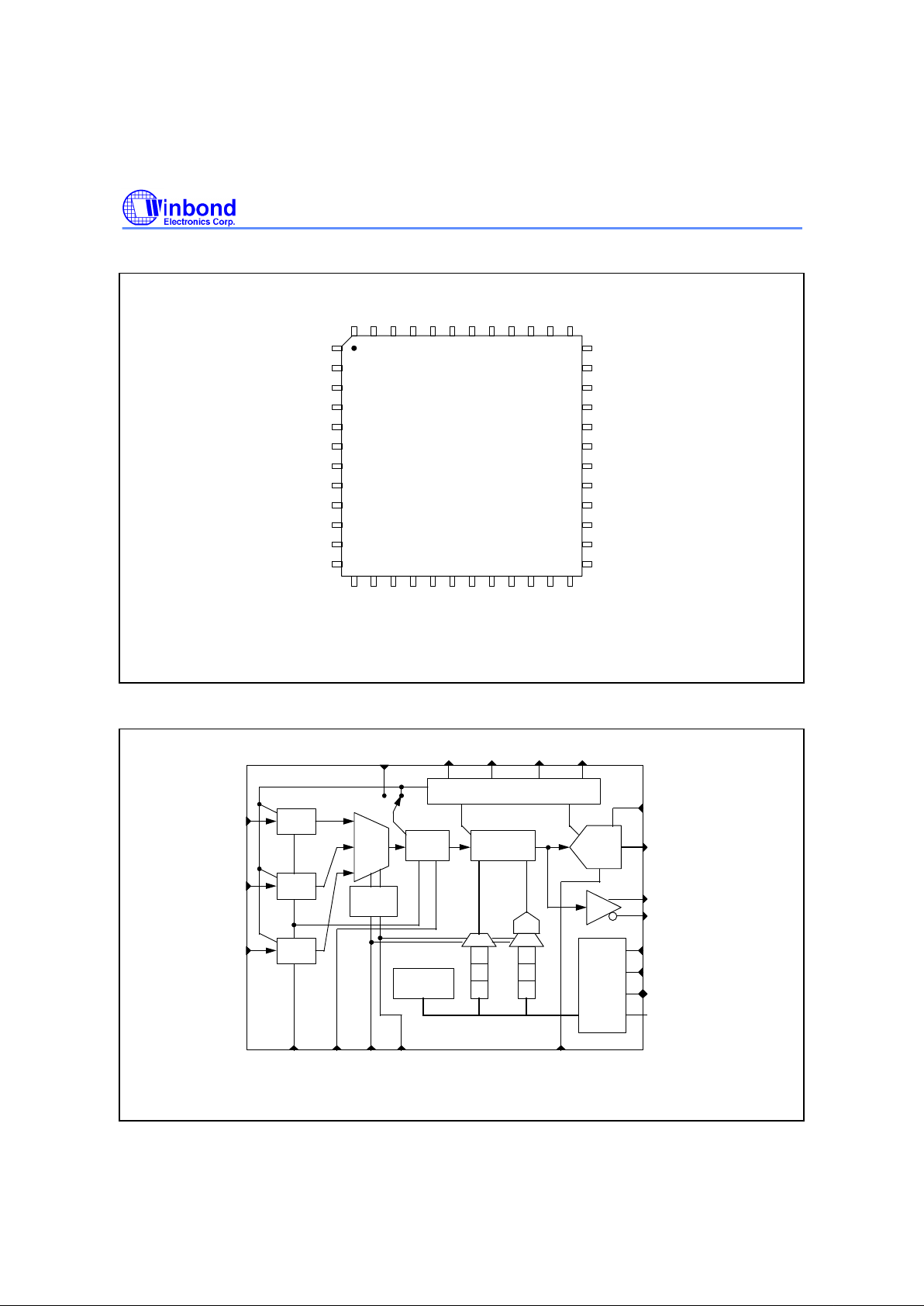
Fig. 3-1 Pin Assignments.
PAOUT
PAOUTN
AVDD
AVSS
VRDT
VRDT
VRDB
VRDB
VREF
VRDC
VINR
AVSS
VING
AVSS
VINB
AVSS
CISREF
CDSCK1
ADCCLK
CDSCK2
DRVSS
DRVDD
AVDD
SEL0
SCLK
SDI/SDIO
SDO/SMS
SEN
DOUT0
DOUT1
DOUT2
DOUT3
DOUT4
AVSS
AVDD
DOUT6
DOUT7
DOUT8
DOUT9
DOUT10
DOUT11
OEN
1
2
3
4
5
6
7
8
9
10
11
12
13 14 15 16 17 18 19 20 21 22 23 24
25
26
27
28
29
30
31
32
33
34
35
36
3738394041424344
DOUT5
SEL1
NC
NC
NC
NC
45464748
W6662CF
Winbond
4. BLOCK DIAGRAM
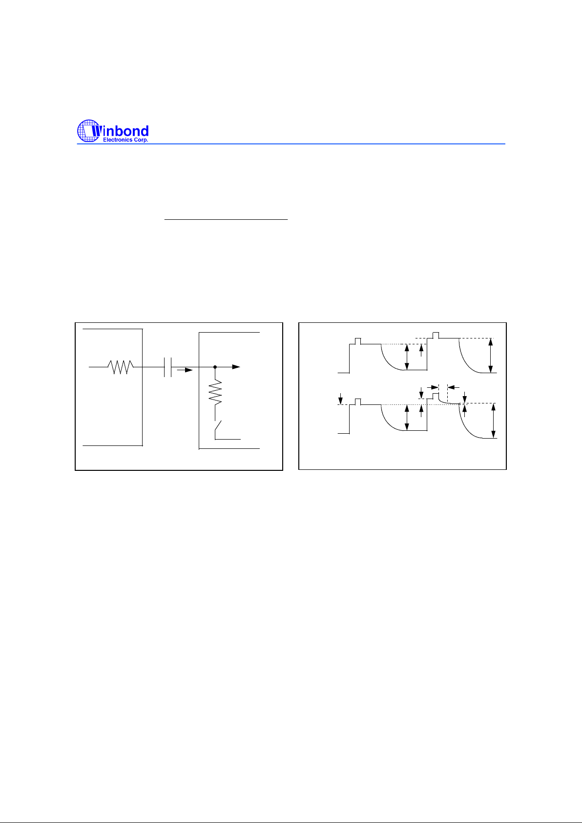
Fig. 4 The Block Diagram of W6662 Device.
Clamp
MUX
12-bit
ADC
Serial
I/O port
control
Bandgap Reference Circuit
Clamp
Gain/Offset
Adjust
Clamp
VINR
VING
VINB
CDSCK1 CDSCK2
DOUT[11:0]
SCLK
SEN
SDI/SDIO
DAC
Offset
Registers
Gain
Registers
Configuration
Register
CISREF
PAOUT
PAOUTN
R
G
B
OEN
ADCCLK
R
G
B
MUX MUX
SEL0 SEL1
CDS
Process
I/P MUX
Ctrl
SDO/SMS
Weak
Drive
CDS
VREF VRDC VRDB VRDT

Preliminary W6662CF
Publication Release Date: December 1998
- 3 - Revision A1
5. PIN DESCRIPTIONS
PIN NAME TYPE DESCRIPTION
10, 37, 44 AVDD AP Analog Power Supply.
4, 6, 8, 35, 42 AVSS AP Analog Ground.
45, 46 VRDT AO Voltage Reference Decoupling (Top).
47, 48 VRDB AO Voltage Reference Decoupling (Bottom).
1 VRDC AO Voltage Reference Decoupling (Center).
2 VREF AO Internal Reference Output.
3 VINR AI Analog Input, Red Channel.
5 VING AI Analog Input, Green Channel.
7 VINB AI Analog Input, Blue Channel.
11 CISREF AI Reference Voltage Input when CIS input.
12 PAOUT AO PGA Output, low speed analog monitor output for test only.
13 PAOUTN AO PGA Output (negative), low speed analog monitor output for
test only.
14 CDSCK1 DI CDS Clock 1 (Schmitt Trigger Input), Reset Level Sampling
Clock.
15 CDSCK2 DI CDS Clock 2 (Schmitt Trigger Input), Data Level Sampling
Clock.
16 ADCCLK DI A/D Converter Sampling Clock (Schmitt Trigger Input).
19 DRVDD DP Digital Driver Power Supply.
17 DRVSS DP Digital Driver Ground.
20 SEL0 DI Channel Select bit 0.
21 SEL1 DI Channel Select bit 1.
22 SCLK DI Clock Input of Serial Interface (Schmitt Trigger Input).
23 SDI/SDIO DI/DO Serial Interface of Data Input or Serial Interface of Data
Input/Output.
24 SDO/SMS DI, DO Serial Interface of Data Output, Serial Interface Mode
Select.
25 SEN DI Enable Signal of Serial Interface, Active Low.
26:34 DOUT[0:8] DO Data Output Bit, DOUT0 is LSB.
38:40 DOUT[9:11] DO Data Output Bit, DOUT11 is MSB.
41 OEN DI Output Enable, Active Low.
Type: AP is Analog Power, AI is Analog Input, AO is Analog Output, DP is Digital Power, DI is Digital Input, DO is Digital
Output.

Preliminary W6662CF
- 4 -
6. FUNCTIONAL DESCRIPTIONS
Figure 4 is the block diagram of W6662, it consists of three channel clamp circuit for CDS mode, a
multiplexer to mux 3-channel inputs and outputs to a correlated double sampling (CDS), a
programmable gain control and offset adjustment amplifier, a 12-bit analog-to-digital converter.
Bandgap reference circuit generate voltage reference signals for input signals clampping and
correlated sampling use (in CDS mode), for offset D/A converter and output A/D converter use. The
select signals SEL1 and SEL0 are used to select the offset registers and gain registers, the input
channels may be selected simultaneously.
6.1 Clamp Circuit
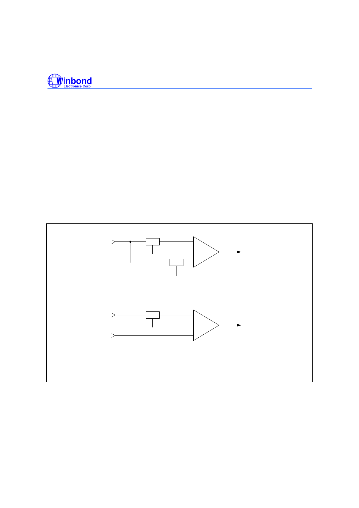
The capacitor between the output of CCD/CIS device and W6662 is used to block the DC voltage
(even as high voltage). The clamp circuit is used to remove unwanted common-mode voltage in the
input pixel data and to get a maximum input signal span when the input is driven by CCD device as
shown in Figure 6-1. The input pins of W6662 are clampped to a internal offset voltage while valid
pixel signal is input. The clamp switches at three channels of figure 6-1 are turn on whenever
CDSCK1 goes high. Figure 6-2 shows the waveform between output of CCD device and input of
W6662, the voltage change on the capacitor will be clampped.
The value of input capacitor is calculated as follows:
tCLP
CMAX =
(RON + RCCDS) × ln (VC/VCLPTolerance)
IBIAS × tC2I
CMIN =
dV
where
CMAX is the maximum capacitor value.
CMIN is the minimum capacitor value.
tCLP is the high pulse width of the CDSCK1 clock input.
RON is switch resistance during clampping and is equivalent to 5K.
RCCDS is the source resistance of CCD device.
VC is the voltage change on the input capacitor must be clampped.
VCLPTolerance is the tolerance voltage error at the end of clampping.
IBIAS is the input leakage current on the input of the W6662 device.
dV is the maximum voltage drift on the input of the W6662 device.
tC2I is the time stamp from the end of clampping point to the acture input data sampling point, equal
to tC2S + tSPD + tACD or may be approximated as conversion time tCVR.

Preliminary W6662CF
Publication Release Date: December 1998
- 5 - Revision A1
If input capacitor value is specified as CIN, the following is the equation to calculate how many lines
are required before the capacitor settles to the desired accuracy after power is up:
(RON + RCCDS) × CIN
LN = ln (VOFS/VCLPTolerance )
PIXN × tCLP
where
LN is line number.
PIXN is the total pixel number in one line.
CIN is the input capacitor value, 0.01 µF is suggestion value.
VOFS is the internal offset voltage to be clampped on the input terminal of the input capacitor.
Fig. 6-1 Equivalent Circuit of Clampping.
R
ON
= 5K
R
CCDS
C
IN
Input to MUX
V
OFS
W6662
CCD Device
I
BIAS
on when
CDSCK1= high
0.01uF
Fig. 6-2 CCD Input Clamp Waveform.
Output
signal
from CCD
Input
signal
to W6662
V
C
(Pixel n)
(Pixel n+1)
t
CLP
V
CLPTolerance
V
C
V
DATAn
V
DATAn
V
DATAn+1
V
DATAn+1
V
OFS
6.2 MUX and Channel Select
The analog input signal may be three channels or single channel and is specified in configuration
register. Three channel input or single channel input are described as follows:
The three channel input is used for red, green and blue analog signal input, selected by SEL1 and
SEL0 signals. The channel select signals SEL1 and SEL0 may be 01, 10, 11 and listed as follows:
SEL1 = 0, SEL0 = 1 is red channel input selected, red channel of gain register and offset register also
selected.
SEL1 = 1, SEL0 = 0 is green channel input selected, green channel of gain register and offset register
also selected.
SEL1 = 1, SEL0 = 1 is blue channel input selected, blue channel of gain register and offset register
also selected.
SEL1 = 0, SEL0 = 0 is reserved.
The one channel input is used for black and white CCD/CIS sensor or multiplexed color CCD/CIS
sensor output. Any channel input of red, green or blue can be used, other un-used analog input must
tight to VSS in S & H mode. The channel select signals SEL1 and SEL0 is used to select offset
register and gain register only and may be 01, 10, 11, described as follows:

Preliminary W6662CF
- 6 -
SEL1 = 0, SEL0 = 1 is red channel of gain register and offset register selected.
SEL1 = 1, SEL0 = 0 is green channel of gain register and offset register selected.
SEL1 = 1, SEL0 = 1 is blue channel of gain register and offset register selected.
SEL1 = 0, SEL0 = 0 is reserved.
6.3 CDS vs S&H Mode
"CDS" stands for "correlated double sampling". It is used to reduce noise generated in CCD source
and to decrease the sampling error which induced from clampping voltage error. CDS takes two step
to sample a CCD's output pixel. In the first step, the reset level of CCD output is sampled and hold by
S/H1 at the falling edge of CDSCK1 signal. In the second step, the data signal of CCD output is
sampled and hold by S/H2 at the falling edge of CDSCK2 signal. The CDS output voltage is obtained
from the voltage difference of the outputs of S/H1 and S/H2.
In S&H mode, the data signal of CIS output is sampled and hold by S/H1 at the falling edge of
CDSCK2 signal and the output voltage is obtained from the voltage difference of the outputs of S/H1
and CISREF pin. Figure 6-3 shows the equivalent circuits of CDS and S&H mode processing.
Fig. 6-3 The Equivalent Circuit of CDS and S&H Mode.
S/H1
S/H2
CDSCK1
CDSCK2
+
-
From
I/P
MUX
To
Gain/Offset
Adjust
S/H1
CDSCK2
+
-
From
I/P
MUX
To
Gain/Offset
Adjust
(a) CDS Mode.
(b) S&H Mode.
From
CISREF
pin
6.4 Gain/Offset Adjustment
The analog input signal after CDS or S&H processed is amplified by PGA gain adjustment and then
shifted by offset value. The offset value will not affected by the PGA gain adjustment.
 Loading...