Winbond Electronics W6692 Datasheet

Preliminary Data Sheet
W6692 PCI ISDN S/T-Controller
W6692
PCI Bus ISDN S/T-Controller
Data Sheet
-1 -
Publication Release Date: Sep 30, 1999

Preliminary Data Sheet
W6692 PCI ISDN S/T-Controller
The information described in this document is the exclusive intellectual property of Winbond
Electronics Corp and shall not be reproduced without permission from Winbond.
Winbond is providing this document only for reference purposes for W6692-based system design.
Winbond assumes no responsibility for errors or omissions. All data and specifications are subject to
change without notice.
-2 -
Publication Release Date: Sep 30, 1999

Preliminary Data Sheet
W6692 PCI ISDN S/T-Controller
TABLE OF CONTENTS
1. GENERAL DESCRIPTION..........................................................................................................9
2. FEATURES ...................................................................................................................................9
3. PIN CONFIGURATION ............................................................................................................10
4. PIN DESCRIPTION ...................................................................................................................13
5. SYSTEM DIAGRAM AND APPLICATIONS ...........................................................................16
6. BLOCK DIAGRAM....................................................................................................................17
7. FUNCTIONAL DESCRIPTIONS...............................................................................................18
7.1 Main Block Functions......................................................................................................................................................18
7.2 Layer 1 Functions Descriptions .......................................................................................................................................19
7.2.1 S/T Interface Transmitter/Receiver .............................................................................................................................19
7.2.2 Receiver Clock Recovery And Timing Generation ......................................................................................................24
7.2.3 Layer 1 Activation/Deactivation.................................................................................................................................. 24
7.2.3.1 States Descriptions And Command/Indication Codes...........................................................................................24
7.2.3.2 State Transition Diagrams....................................................................................................................................26
7.2.4 D Channel Access Control..........................................................................................................................................30
7.2.5 Frame Alignment........................................................................................................................................................30
7.2.5.1 FAinfA_1fr.......................................................................................................................................................... 31
7.2.5.2 FAinfB_1fr .......................................................................................................................................................... 31
7.2.5.3 FAinfD_1fr.......................................................................................................................................................... 32
7.2.5.4 FAinfA_kfr.......................................................................................................................................................... 32
7.2.5.5 FAinfB_kfr .......................................................................................................................................................... 33
7.2.5.6 FAinfD_kfr.......................................................................................................................................................... 33
7.2.5.7 Faregain............................................................................................................................................................... 34
7.2.6 Multiframe Synchronization ....................................................................................................................................... 34
7.2.7 Test Functions ............................................................................................................................................................ 36
7.3 Serial Interface Bus.........................................................................................................................................................38
7.4 B Channel Switching.......................................................................................................................................................38
7.5 PCM Port.........................................................................................................................................................................40
7.6 D Channel HDLC Controller.......................................................................................................................................... 40
7.6.1 D Channel Message Transfer Modes ...........................................................................................................................41
-3 -
Publication Release Date: Sep 30, 1999

Preliminary Data Sheet
W6692 PCI ISDN S/T-Controller
7.6.2 Reception of Frames in D Channel..............................................................................................................................41
7.6.3 Transmission of Frames in D Channel........................................................................................................................ 42
7.7 B Channel HDLC Controller..........................................................................................................................................43
7.7.1 Reception of Frames in B Channel ......................................................................................................................... 43
7.7.2 Transmission of Frames in B Channel ........................................................................................................................ 44
7.8 GCI Mode Serial Interface Bus.......................................................................................................................................45
7.8.1 GCI Mode C/I0 Channel Handling..............................................................................................................................46
7.8.2 GCI Mode Monitor Channel Handling ........................................................................................................................46
7.9 PCI/MP Interface Circuit................................................................................................................................................48
7.9.1 PCI Slave Mode And Configuration Serial EEPROM .................................................................................................48
7.9.2 8-bit Microprocessor Interface.....................................................................................................................................49
7.10 Peripheral Control......................................................................................................................................................... 49
8. REGISTER DESCRIPTIONS ......................................................................................................51
8.1 Chip Control and D_ch HDLC controller ......................................................................................................................51
8.1.1 D_ch receive FIFO D_RFIFO Read Address 00H/00H ...........................................................................................53
8.1.2 D_ch transmit FIFO D_XFIFO Write Address 04H/01H.........................................................................................53
8.1.3 D_ch command register D_CMDR Read/Write Address 08H/02H ...........................................................................54
8.1.4 D_ch Mode Register D_MODE Read/Write Address 0CH/03H................................................................................54
8.1.5 Timer 1 Register TIMR1 Read/Write Address 10H/04H ........................................................................................55
8.1.6 Interrupt Status Register ISTA Read_clear Address 14H/05H .............................................................................56
8.1.7 Interrupt Mask Register IMASK R/W Address 18H/06H..........................................................................................57
8.1.8 D_ch Extended Interrupt Register D_EXIR Read_clear Address 1CH...................................................................... 57
8.1.9 D_ch Extended Interrupt Mask Register D_EXIM Read/Write Address 20H/08H ....................................................58
8.1.10 D_ch Status Register D_XSTA Read Address 24H/09H ..................................................................................... 58
8.1.11 D_ch Receive Status Register D_RSTA Read Address 28H/0AH.........................................................................59
8.1.12 D_ch SAPI Address Mask D_SAM Read/Write Address 2CH/0BH......................................................................59
8.1.13 D_ch SAPI1 Register D_SAP1 Read/Write Address 30H/0CH.............................................................................60
8.1.14 D_ch SAPI2 Register D_SAP2 Read/Write Address 34H/0DH...............................................................................60
8.1.15 D_ch TEI Address Mask D_TAM Read/Write Address 38H/0EH ......................................................................... 60
8.1.16 D_ch TEI1 Register D_TEI1 Read/Write Address 3CH/0FH................................................................................61
8.1.17 D_ch TEI2 Register D_TEI2 Read/Write Address 40H/10H ................................................................................61
8.1.18 D_ch Receive Frame Byte Count High D_RBCH Read Address 44H/11H ............................................................61
8.1.19 D_ch Receive Frame Byte Count Low D_RBCL Read Address 48H/12H............................................................. 62
8.1.20 Timer 2 TIMR2 Write Address 4CH/13H.......................................................................................... 62
8.1.21 Layer 1_Ready Code L1_RC Read/Write Address 50H/14H...............................................................62
8.1.22 Control Register CTL Read/Write Address 54H/15H ............................................................................................. 63
8.1.23 Command/Indication Receive Register CIR Read Address 58H/16H.................................................................... 63
8.1.24 Command/Indication Transmit Register CIX Read/Write Address 5CH/17H........................................................64
8.1.25 S/Q Channel Receive Register SQR Read Address 60H/18H..............................................................................64
8.1.26 S/Q Channel Transmit Register SQX Read/Write Address 64H/19H ..................................................................65
8.1.27 Peripheral Control Register PCTL Read/Write Address 68H/1AH.................................................................... 65
8.1.28 Monitor Receive Channel 0 MO0R Read Address 6CH/1BH............................................................................ 66
8.1.29 Monitor Transmit Channel 0 MO0X Read/Write Address 70H/1CH.................................................................67
8.1.30 Monitor Channel 0 Interrupt Register MO0I Read_clear Address 74H/1DH......................................................67
8.1.31 Monitor Channel 0 Control Register MO0C Read/Write Address 78H/1EH..........................................................67
-4 -
Publication Release Date: Sep 30, 1999

Preliminary Data Sheet
W6692 PCI ISDN S/T-Controller
8.1.32 GCI Mode Control/Status Register GCR Read/Write Address 7CH/1FH.......................................68
8.1.33 Peripheral Address Register XADDR Read/Write Address F4H/3DH............................................................... 69
8.1.34 Peripheral Data Register XDATA Read/Write Address F8H/3EH..................................................................... 70
8.1.35 Serial EEPROM Control Register EPCTL Read/Write Address FCH/3FH ............................................................71
8.1.36 Monitor Receive Channel 1 Register MO1R Read Address 6DH/40H.................................................................71
8.1.37 Monitor Transmit Channel 1 MO1X Read/Write Address 71H/41H..................................................................72
8.1.38 Monitor Channel 1 Interrupt Register MO1I Read_clear Address 75H/42H ...................................................... 72
8.1.39 Monitor Channel 1 Control Register MO1C Read/Write Address 79H/43H..........................................................72
8.1.40 GCI IC1 Receive Register IC1R Read Address 6EH/44H................................................................................ 73
8.1.41 GCI IC1 Transmit Register IC1X Read/Write Address 72H/45H.....................................................................73
8.1.42 GCI IC2 Receive Register IC2R Read Address 6FH/46H................................................................................73
8.1.43 GCI IC2 Transmit Register IC2X Read/Write Address 73H/47H.....................................................................73
8.1.44 GCI CI1 Indication Register CI1R Read Address 7DH/48H............................................................................ 74
8.1.45 GCI CI1 Command Register CI1X Read/Write Address 7EH/49H..................................................................74
8.1.46 GCI Extended Interrupt Register GCI_EXIR Read_clear Address 76H/4AH .......................................................... 74
8.1.47 GCI Extended Interrupt Mask Register GCI_EXIM Read/Write Address 7AH/4BH............................................... 75
8.2 B1 HDLC controler......................................................................................................................................................... 75
8.2.1 B1_ch receive FIFO B1_RFIFO Read Address 80H/20H .....................................................................................76
8.2.2 B1_ch transmit FIFO B1_XFIFO Write Address 84H/21H.................................................................................76
8.2.3 B1_ch command register B1_CMDR Read/Write Address 88H/22H....................................................................77
8.2.4 B1_ch Mode Register B1_MODE Read/Write Address 8CH/23H.......................................................................... 78
8.2.5 B1_ch Extended Interrupt Register B1_EXIR Read_clear Address 90H/24H............................................................79
8.2.6 B1_ch Extended Interrupt Mask Register B1_EXIM Read/Write Address 94H/25H................................................. 80
8.2.7 B1_ch Status Register B1_STAR Read Address 98H/26H...................................................................................... 80
8.2.8 B1_ch Address Mask Register 1 B1_ADM1 Read/Write Address 9CH/27H........................................................... 81
8.2.9 B1_ch Address Mask Register 2 B1_ADM2 Read/Write Address A0H/28H...........................................................81
8.2.10 B1_ch Address Register 1 B1_ADR1 Read/Write Address A4H/29H...................................................................81
8.2.11 B1_ch Address Register 2 B1_ADR2 Read/Write Address A8H/2AH..................................................................82
8.2.12 B1_ch Receive Frame Byte Count Low B1_RBCL Read Address ACH/2BH..........................................................82
8.2.13 B1_ch Receive Frame Byte Count High B1_RBCH Read Address B0H/2CH ......................................................... 82
8.2.14 B1_ch Transmit Idle Pattern B1_IDLE Read/Write Address B4H/2DH ..................................................................83
8.3 B2 HDLC controller........................................................................................................................................................83
8.4 PCI Configuration Register............................................................................................................................................. 84
8.4.1 Device/Vendor ID Register Read Address 00 H.................................................................................................85
8.4.2 Status/Command Register Read/Write Address 04H...........................................................................................85
8.4.3 Class Code/Revision ID Register Read Address 08H..........................................................................................87
8.4.4 Header Type/Latency Timer Register Read Address 0CH....................................................................................87
8.4.5 Base Address Register 0 Read/Write Address 10H............................................................................................88
8.4.6 Base Address Register 1 Read/Write Address 14H.............................................................................................89
8.4.7 Subsystem/Subsystem Vendor ID Register Read Address 2CH...........................................................................89
8.4.8 Interrupt Line Register Read/Write Address 3CH...............................................................................................90
8.4.9 Capability Pointer Read Address 34H................................................................................................................90
8.4.10 Power Management Capability Read Address 40H...........................................................................................91
8.4.11 Power Management Control/Status Read/Write Address 44H...........................................................................92
9. ELECTRICAL CHARACTERISTICS...........................................................................................94
9.1 Absolute Maximum Rating ..............................................................................................................................................94
-5 -
Publication Release Date: Sep 30, 1999

Preliminary Data Sheet
W6692 PCI ISDN S/T-Controller
9.2 Power Supply................................................................................................................................................................... 94
9.3 DC Characteristics..........................................................................................................................................................94
9.4 Preliminary Switching Characteristics...........................................................................................................................96
9.4.1 PCM Interface Timing1)..............................................................................................................................................96
9.4.2 Serial EEPROM Timing.............................................................................................................................................97
9.4.3 Peripheral Interface Timing........................................................................................................................................ 97
9.4.5 8-bit Microprocessor Timing.......................................................................................................................................98
9.5 AC Timing Test Conditions ...........................................................................................................................................101
10. PACKAGE SPECIFICATIONS................................................................................................102
-6 -
Publication Release Date: Sep 30, 1999

Preliminary Data Sheet
W6692 PCI ISDN S/T-Controller
LIST OF FIGURES
FIG.3.1 W6692 PIN CONFIGURATION - PCI MODE.......................................................................................................... 10
FIG.3.2 W6692 PIN CONFIGURATION - INTEL BUS MODE............................................................................................11
FIG.3.3 W6692 PIN CONFIGURATION - MOTOROLA BUS MODE.................................................................................12
FIG.5.1 ISDN INTERNET PASSIVE S-CARD WITH TWO POTS CONNECTIONS ......................................................... 16
FIG.6.1 W6692 FUNCTIONAL BLOCK DIAGRAM.............................................................................................................17
FIG.7.1 FRAME STRUCTURE AT S/T INTERFACE...........................................................................................................20
FIG.7.2 W6692 WIRING CONFIGURATION IN TE APPLICATIONS...............................................................................21
FIG.7.3 EXTERNAL TRANSMITTER CIRCUITRY ............................................................................................................22
FIG.7.4 EXTERNAL RECEIVER CIRCUITRY..................................................................................................................... 22
FIG.7.5 LAYER 1 ACTIVATION/DEACTIVATION STATE DIAGRAM - NORMAL MODE ..........................................28
FIG.7.6 LAYER 1 ACTIVATION/DEACTIVATION STATE DIAGRAM - SPECIAL MODE ...........................................29
FIG.7.7 SSP AND SCP TEST SIGNALS..................................................................................................................................37
FIG 7.8 GCI MODE CHANNEL STRUCTURE.....................................................................................................................46
FIG.7.9 SERIAL EEPROM DATA LAYOUT .........................................................................................................................48
-7 -
Publication Release Date: Sep 30, 1999

Preliminary Data Sheet
W6692 PCI ISDN S/T-Controller
LIST OF TABLES
TABLE 4.1 W6692 PIN DESCRIPTIONS ........................................................................................................................... 13
TABLE 7.1 OUTPUT PHASE DELAY COMPENSATION TABLE ................................................................................. 24
TABLE 7.2 LAYER 1 COMMAND CODES....................................................................................................................... 26
TABLE 7.3 LAYER 1 INDICATION CODES..................................................................................................................... 26
TABLE 7.4 D PRIORITY CLASSES................................................................................................................................... 30
TABLE 7.5 D PRIORITY COMMANDS/INDICATIONS..................................................................................................30
TABLE 7.6 MULTIFRAME STRUCTURE IN S/T INTERFACE.....................................................................................35
TABLE 8.1 REGISTER ADDRESS MAP : CHIP CONTROL AND D CHANNEL HDLC ..............................................51
TABLE 8.2 REGISTER SUMMARY : CHIP CONTROL AND D CHANNEL HDLC ..................................................52
TABLE 8.3 REGISTER ADDRESS MAP : B1 CHANNEL HDLC....................................................................................75
TABLE 8.4 REGISTER SUMMARY : B1 CHANNEL HDLC ...........................................................................................76
TABLE 8.5 REGISTER ADDRESS MAP : B2 CHANNEL HDLC....................................................................................83
TABLE 8.6 REGISTER SUMMARY : B2 CHANNEL HDLC ...........................................................................................83
TABLE 8.7 PCI CONFIGURATION SPACE ...................................................................................................................84
-8 -
Publication Release Date: Sep 30, 1999

Preliminary Data Sheet
W6692 PCI ISDN S/T-Controller
1. GENERAL DESCRIPTION
The Winbond's single chip PCI bus ISDN S/T interface controller (W6692) is an all-in-one device suitable for ISDN Internet
access. Three HDLC controllers are incorporated in the chip, one for D channel and the other two for B channels. These HDLC
controllers facilitate efficient access to signaling and data services. The PCM codec interface provides voice service or other
services. The built in PCI 2.2 interface circuit makes glueless design for PCI bus add-on card application.
2. FEATURES
* Full duplex 2B + D S/T-interface transceiver compliant with ITU-T I.430 Recommendation
* One D channel HDLC controller
- Maskable address recognition
- Transparent (HDLC) mode
- FIFO buffer (2 x 128 bytes)
* Two B channel HDLC controllers
- Maskable address recognition
- Bit rate options : 56 or 64 kbps
- Transparent (HDLC mode) or extended transparent mode (clear channel)
- FIFO buffer (2 x 128 bytes) per B channel
* Two PCM codec interfaces for speech and POTS application
* Various B channel switching capabilities
* GCI master/slave interface
* Built in PCI 2.2 slave mode circuit
* ACPI capability : PCI 2.2 and PCI Power Management 1.1 compliant
* Serial EEPROM interface for PCI configuration
* Peripheral control pins
* 8-bit microprocessor interface when PCI is disabled for TA application
* Digital : 5V or 3.3V, analog : 5V
* Advanced CMOS technology
* Low power consumption
* 100-pin QFP package
-9 -
Publication Release Date: Sep 30, 1999

Preliminary Data Sheet
3. PIN CONFIGURATION
W6692 PCI ISDN S/T-Controller
22232
C
/
B
E
1
#
V
A
U
X
X
X
I
I
/
X
N
N
X
V
V
T
T
T
T
D
D
A
S
S
I
I
A
D
D
L
X
X
N
N
L
A
D
1
1
2
2
1
0
5
51525
55565
5
SR2
8
A
D
1
5
50
3
7
4
SR1
49
VSSA
48
47
AD0
46
AD1
AD2
45
AD3
44
VDDB
43
VSSB
42
AD4
41
AD5
40
39
AD6
38
AD7
37
C/BE0#
AD8
36
35
AD9
AD10
34
33
AD11
32
VDDB
27282
2
2
31
4
5
A
A
D
D
1
1
3
4
VSSB
6
930
I
I
I
I
A
O
O
O
O
D
4
6
5
7
1
/
/
/
/
2
X
X
X
X
A
A
A
A
D
D
D
D
4
6
5
7
RST#
VSSD
VDDD
CLK
AD31
AD30
AD29
VSSB
VDDB
AD28
AD27
AD26
AD25
AD24
C/BE3#
IDSEL
AD23
AD22
AD21
AD20
I
I
I
O
O
O
1
8
9
0
/
I
E
E
/
/
X
E
E
N
P
P
X
X
A
F
P
D
P
T
S
S
R
W
L
DDD
S
C
C
S
A
D
D
D
R
#
E
B
B
8
81
0
82
83
84
85
86
87
88
89
90
91
92
93
94
95
96
97
98
99
100
2
3 7456
1
I
I
I
O
O
O
2
0
1
/
/
/
X
X
X
A
A
A
D
D
D
2
0
1
U
C
I
O
S
L
K
73747
576777879
1
101
8
9
1
I
A
C
A
A
A
V
V
O
D
/
D
D
D
D
S
3
1
B
1
1
1
D
S
7
E
6
8
9
B
B
/
2
X
#
A
D
3
P
V
P
V
P
F
D
T
S
R
C
D
X
S
X
K
D
D
1
D
D
666
6
4
5
76869707172
W6692
ISDN-PCI
1
2
3
6
I
F
V
T
D
R
R
S
R
E
D
A
S
D
V
Y
M
D
S
Y
#
E
E
#
#
L
#
T
P
P
V
P
E
F
M
S
B
S
C
E
S
C
T
K
#
D
K
P
2
60596
636
6
1
2
1
1714151
19202
8
1
P
T
P
V
S
E
O
A
D
T
R
U
R
D
O
R
T
D
P
2
#
#
FIG.3.1 W6692 PIN CONFIGURATION - PCI MODE
-10 -
Publication Release Date: Sep 30, 1999

Preliminary Data Sheet
W6692 PCI ISDN S/T-Controller
I
I
I
O
RST#
VSSD
VDDD
CLK
VSSB
VDDB
O
O
1
8
9
0
/
/
/
I
X
X
X
N
T
#
8
81
0
82
83
84
85
86
87
88
89
90
91
92
93
94
95
96
97
98
99
100
W
R
B
9
2 3 74 5 6
1
I
I
O
O
0
1
/
/
X
X
A
A
D
D
0
1
D
F
A
R
C
D
S
L
D
L
C
E
B
DDU
7
747
77787
7
3
2
5
6
1
1891013121714151618192021
I
V
V
I
O
D
S
O
2
D
S
3
/
B
/
B
X
X
A
A
D
D
2
3
P
V
V
F
P
P
D
S
C
T
R
D
S
K
X
X
D
D
1
D
D
6
6
67686970717
4
6
5
W6692
ISDN-PCI
C
V
A
S
S
L
#
S
E
D
T
P
P
E
F
B
S
C
C
T
K
K
P
2
636
6
2
V
D
D
D
X
X
I
I
X
X
N
N
V
V
V
T
T
T
T
D
D
S
A
S
A
S
I
I
D
D
S
L
X
X
N
N
L
A
D
1
D
1
2
1
0
2
5
22232
W
R
#
515
55565
5
SR2
7
4
2
2
627282930
5
I
O
4
/
X
A
D
4
50
253
4
SR1
49
VSSA
48
47
AD0
46
AD1
AD2
45
AD3
44
VDDB
43
VSSB
42
AD4
41
AD5
40
39
AD6
38
AD7
37
RD#
36
35
34
33
32
VDDB
31
VSSB
I
I
I
O
O
O
6
5
7
/
/
/
X
X
X
A
A
A
D
D
D
6
5
7
8
6
5
0
961
T
O
U
T
2
FIG.3.2 W6692 PIN CONFIGURATION - INTEL BUS MODE
-11 -
Publication Release Date: Sep 30, 1999

Preliminary Data Sheet
W6692 PCI ISDN S/T-Controller
I
I
I
O
RST#
VSSD
VDDD
CLK
VSSB
VDDB
O
O
1
8
9
0
/
/
/
I
X
X
X
N
T
#
8
81
0
82
83
84
85
86
87
88
89
90
91
92
93
94
95
96
97
98
99
100
W
R
B
9
2 3 74 5 6
1
I
I
O
O
0
1
/
/
X
X
A
A
D
D
0
1
D
F
A
R
C
D
S
L
D
L
C
E
B
DDU
7
747
77787
7
3
2
5
6
1
1891013121714151618192021
I
V
V
I
A4A
A6A
O
D
S
O
5
7
2
D
S
3
/
B
/
B
X
X
A
A
D
D
2
3
P
V
V
F
P
P
D
S
C
T
R
D
S
K
X
X
D
D
1
D
D
6
6
67686970717
4
6
5
W6692
ISDN-PCI
C
V
S
S
#
S
D
T
P
P
E
F
B
S
C
C
T
K
K
P
2
636
6
2
V
D
D
D
X
X
I
I
X
X
N
N
V
V
V
T
T
T
T
D
D
S
A
S
A
S
I
I
D
D
S
L
X
X
N
N
L
A
D
1
D
1
2
1
0
2
5
22232
D
S
#
515
55565
5
SR2
7
4
2
2
627282930
5
I
O
4
/
X
A
D
4
50
253
4
SR1
49
VSSA
48
47
D0
46
D1
D2
45
D3
44
VDDB
43
VSSB
42
D4
41
D5
40
39
D6
38
D7
37
RW
36
A0
A1
35
A2
34
A3
33
32
VDDB
31
VSSB
I
I
I
O
O
O
6
5
7
/
/
/
X
X
X
A
A
A
D
D
D
6
5
7
8
6
5
0
961
T
O
U
T
2
FIG.3.3 W6692 PIN CONFIGURATION - MOTOROLA BUS MODE
-12 -
Publication Release Date: Sep 30, 1999

Preliminary Data Sheet
W6692 PCI ISDN S/T-Controller
4. PIN DESCRIPTION
TABLE 4.1 W6692 PIN DESCRIPTIONS
Notation : The suffix "#" indicates an active LOW signal.
Pin
Name
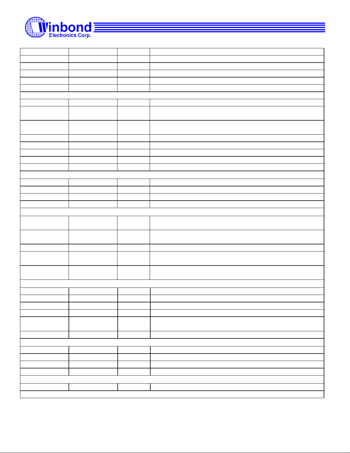
CLK 84 I
AD31-AD0 85,86,87,90,91,
C/BE3#-C/BE0# 95,11,22,37 I Bus command and Byte Enables.
PAR 21 I/O Parity is even parity across AD31-AD0 and C/BE3#-C/BE0#.
FRAME# 12 I FRAME# is asserted to indicate a bus transaction is beginning.
TRDY# 14 O Target Ready indicates W6692 is able to complete the current data
IRDY# 13 I
STOP# 18 O Stop indicates W6692 is requesting the master to stop the current
DEVSEL# 15 O Device Select indicates W6692 has decoded itself as the target of the
IDSEL 96 I Initialization Device Select is used as chip select during configuration
PERR# 19 O Parity Error is used for reporting of data parity errors.
RST# 81 I PCI Reset. RST# may be asynchronous to CLK when asserted or
INTA# 80 O Interrupt. This is level sensitive, active LOW and open drain output.
CLK 84 I This pin must be pulled to HIGH.
AD7-0 38,39,40,41,44,45
Pin
Number
92,93,94,97,98,
99,100,7,8,9,10,
23,24,25,30,33,
34,35,36,38,39,
40,41,44,45,46,
47
,46,47
Type Functions
PCI Bus
PCI Mode : PCI Clock. All other PCI signals, except RST#, INTA# are
sampled on the rising edge of CLK. According to PCI 2.1/2.2
specification, CLK is stable at least 100 µs (Trst-clk) before deassertion
of RST#.
Intel Bus Mode : Must be pulled to HIGH.
Motorola Bus Mode : Must be pulled to LOW.
I/O Address and Data are multiplexed on the same PCI pins. During the
address phase, AD31-0 contain a 32-bit physical address. During the
data phase, AD7-AD0 contain the least significant byte and AD31AD24 contain the most significant byte.
During the address phase of a transaction, they define the bus
command.
During data phase, they are used as Byte Enables.
phase of the transaction.
Initiator Ready indicates the bus master′s ability to complete the current
data phase of the transaction.
transaction.
current access.
transactions.
deasserted.
Intel Bus Mode (Selected when CLK=HIGH)
I/O Multiplexed address and data. During the address phase, AD7-0 contain
a 8-bit physical address. During the data phase, AD7-AD0 contain data.
-13 -
Publication Release Date: Sep 30, 1999
Preliminary Data Sheet
W6692 PCI ISDN S/T-Controller
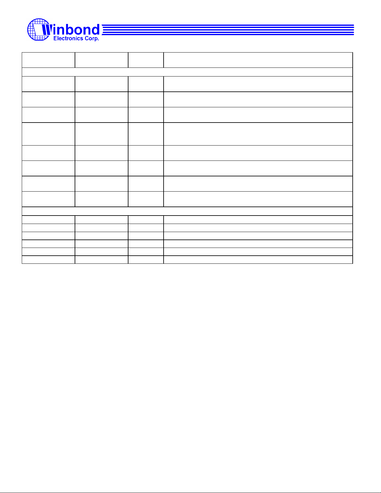
CS# 12 I Chip select.
ALE 13 I Address Latch Enable. Used to latch addresses.
RD# 37 I Read.
WR# 22 I Write.
RST# 81 I Reset.
INT# 80 O Interrupt. This is a level sensitive, active LOW and open drain output.
Motorola Bus Mode (Selected when CLK=LOW)
CLK 84 I This pin must be pulled to LOW.
D7-D0 38,39,40,41,44,45
,46,47
A7-A0 7,8,9,10,33,34,35,
36
CS# 12 I Chip select.
DS# 22 I Data strobe.
RW 37 I Read/write identify. HIGH for read, and LOW for write.
RST# 81 I Reset.
INT# 80 O Interrupt. This is a level sensitive, active LOW and open drain output.
DCL 72 I GCI Bus Data Clock of the frequency: 1.536 MHz.
FSC 71 I GCI Bus Frame Synchronization Clock: 8KHz.
DD 70 I/O GCI Bus Data Downstream : Slave mode - input, master mode - output.
DU 69 I/O GCI Bus Data Upstream : Slave mode - output, master mode - input.
PFCK1 64 O PCM port 1 frame synchronization signal, with 8 KHz repetition rate
PFCK2 62 O PCM port 2 frame synchronization signal, with 8 KHz repetition rate
PBCK 63 O PCM bit synchronization clock of 1.536 MHz.
PTXD 65 O PCM transmit data output. A maximum of two channels with 64 Kbit/s
PRXD 66 I PCM receive data input. A maximum of two channels with 64 Kbit/s
SR1 49 I S/T bus receiver input (negative).
SR2 50 I S/T bus receiver input (positive).
SX1 54 O S/T bus transmitter output (positive).
SX2 55 O S/T bus transmitter output (negative).
XTAL1 56 I Crystal or Oscillator clock input. The clock frequency:
XTAL2 57 O Crystal clock output. Left unconnected when using oscillator.
EPCS 73 O Serial EEPROM chip select (active HIGH).
EPSK 74 O Serial EEPROM data clock (clock frequency < 250 KHz).
EPSDI 76 I Serial EEPROM data input.
EPSDO 75 O Serial EEPROM data output.
TESTP 61 I Used to enable normal operation (1) or enter test mode (0).
I/O Data.
I Address.
GCI Bus
PCM Interface
and 8 bit pulse width.
and 8 bit pulse width.
data rate can be multiplexed on this signal.
data rate can be multiplexed on this signal.
ISDN Signals and External Crystal
7.68MHz±100PPM.
External EEPROM Interface
Functional Test
PCI Power Management
-14 -
Publication Release Date: Sep 30, 1999
Preliminary Data Sheet
W6692 PCI ISDN S/T-Controller
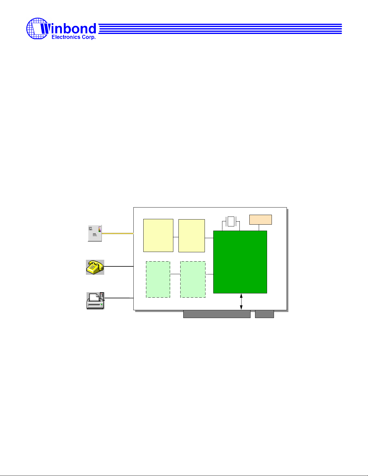
PME 60 O Power Management Event Signal. Level triggered, active HIGH. Drive
a transistor to PME# in PCI slot.
Peripheral Control
TOUT2 20 O Timer 2 output. A square wave with 50 % duty cycle, 1~63 ms period
can be generated.
XINTIN0 52 I A level change (either direction) will generate a maskable interrupt on
the PCI bus interrupt request pin INTA#.
XINTIN1 53 I A level change (either direction) will generate a maskable interrupt on
the PCI bus interrupt request pin INTA#.
IO0-IO10 79,78,77,29,28,
27,26,4,3,2,1
XAD7-XAD0 29,28,27,26,
4,3,2,1
XALE 77 O When configured as microprocessor mode (PCTL:XMODE = 1), this is
XRDB 78 O When configured as microprocessor mode (PCTL:XMODE = 1), this is
XWRB 79 O When configured as microprocessor mode (PCTL:XMODE = 1), this is
VDDD 17,58,67,83 I
VDDA 51 I
VDDB 6,32,43,89 I PCI Bus Power Supply.
VSSD 16,59,68,82 I Digital Ground.
VSSA 48 I Analog Ground.
VSSB 5,31,42,88 I PCI Bus Ground.
I/O When confiured as simple IO mode (PCTL:XMODE = 0), these pins
can read/write data from/to peripheral components. The pin directions
are selected via register.
I/O When configured as microprocessor mode (PCTL:XMODE = 1),
address and data are multiplexed on these pins.
the Address Latch Enable output.
the read pulse.
the write pulse.
Power and Ground
Digital Power Supply (5V±5%).
Analog Power Supply (5V±5%).
-15 -
Publication Release Date: Sep 30, 1999
Preliminary Data Sheet
W6692 PCI ISDN S/T-Controller
5. SYSTEM DIAGRAM AND APPLICATIONS
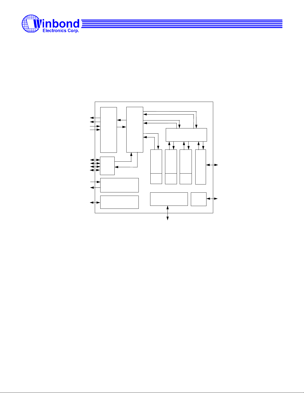
Typical applications include :
- PCI passive S-card for data only service
- PCI passive S-card with one handset/POTS connection
- PCI passive S-card with two POTS connections
- ISDN TA or other embedded application
The all-in-one characteristic of W6692 makes it excellent for passive ISDN PCI card. W6692 integrates three HDLC
controllers in the chip and interfaces to PCI bus directly. In addition, W6692 provides peripheral control circuits for PCM
CODEC and POTS interface.
In the following application, only a few TTL-like glue circuits are needed for the two POTS interface control.
W6692 also integrates the 8-bit Intel or Motorola microprocessor interface which makes it excellent for TA application.
NT
Phone
4-wire S/T
Transformer
Module
POTS
Circuit
x2
Protection
Circuit
W6692
S-Controller
PCM
Codec
x2
EEPROM
PCI
Fax
FIG.5.1 ISDN INTERNET PASSIVE S-CARD WITH TWO POTS CONNECTIONS
-16 -
Publication Release Date: Sep 30, 1999
Preliminary Data Sheet
6. BLOCK DIAGRAM
The block diagram of W6692 is shown in Figure 6.1
2B+D
4-wire S/T
GCI Bus
Line
Transceiver
&
AMI/BIN
Conversion
GCI
Circuit
2B+D
Serial
Interface
(SIB)
Bus
D
HDLC
Controller
W6692 PCI ISDN S/T-Controller
B2
B1
B-channel Switching
D
B1
HDLC
Controller
B2
HDLC
Controller
PCM
Port
PCM CODEC
Crystal/Oscillator
(7.68 MHz)
POTS
circuit
DPLL and Timing Generator
Peripheral Control
FIFO FIFO
PCI/MP Interface Circuit
PCI Bus/Microprocessor
FIFO
Serial
EEPROM
Interface
Serial
EEPROM
FIG.6.1 W6692 FUNCTIONAL BLOCK DIAGRAM
-17 -
Publication Release Date: Sep 30, 1999

Preliminary Data Sheet
W6692 PCI ISDN S/T-Controller
7. FUNCTIONAL DESCRIPTIONS
7.1 Main Block Functions
The functional block diagram of W6692 is shown in Fig.6.1. The main function blocks are :
- Layer 1 function according to ITU-T I.430
- Serial Interface Bus (SIB)
- B channel switching
- GCI bus interface
- PCM port and internal switching (x 2)
- D channel HDLC controller
- B channel HDLC controllers (x 2)
- PCI/microprocessor interface circuit
- Serial EEPROM interface for PCI Configuration purpose
- Peripheral control
The layer 1 function includes:
- S/T bus transmitter/receiver
- Timing recovery using Digital Phase Locked Loop (DPLL) circuit
- Layer 1 activation/deactivation
- D channel access control
- Frame alignment
- Multi-frame synchronization
- Test functions
The serial interface bus performs the multiplexing/demultiplexing of D and 2B channels.
The B channel switching determines the connection between layer1/GCI, layer 2 and PCM.
The GCI circuit is used to connect a U transceiver (slave mode) or other slave GCI device (master mode).
The PCM port provides two 64 kbps clear channels to connect to PCM codec chips and switching between two PCM ports.
The D channel HDLC controller performs the LAPD (Link Access Procedure on the D channel) protocol according to ITU-T
I.441/Q.921 recommendation.
There are two independent B channel HDLC controllers. They can be used to support HDLC-like protocols such as Internet PPP.
Two B channels are also handled by one HDLC controller to support OCN application.
The PCI interface circuit implements PCI specification revision 2.2 slave mode function. When PCI circuit is disabled, a 8-bit
microprocessor interface is used to control the chip.
-18 -
Publication Release Date: Sep 30, 1999

Preliminary Data Sheet
W6692 PCI ISDN S/T-Controller
The peripheral control block is used to control other peripheral devices such as CODEC, SLIC, DTMF detector, LEDs.
7.2 Layer 1 Functions Descriptions
The layer 1 functions includes :
- Transmitter/Receiver which conform to the electrical specifications of ITU-T I.430
- Receiver clock recovery and timing generation
- Output phase delay (deviation) compensation
- Layer 1 activation/deactivation procedures
- D channel access control
- Frame alignment
- Multi-frame synchronization
- Test functions
7.2.1 S/T Interface Transmitter/Receiver
According to ITU-T I.430, pseudo-ternary code with 100% pulse width is used in both directions of transmission on the S/T
interface. The binary "1" is represented by no line signal (zero volt), whereas a binary "0" is represented by a positive or negative
pulse.
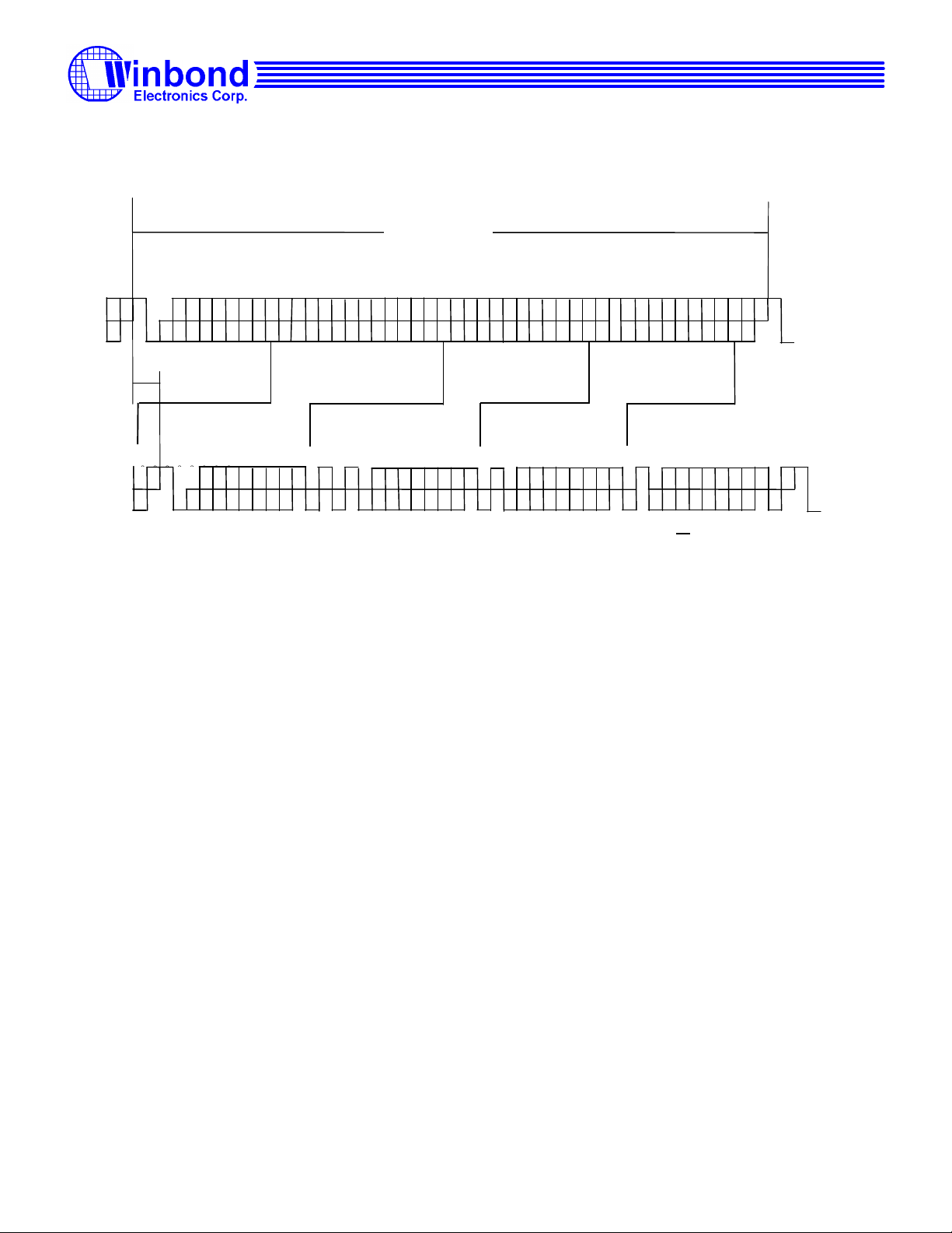
Data transmissions on the S/T interface are arranged as frame structures. The frame is 250 µs long and consists of 48 bits,
which corresponds to a 192 kbit/s line rate. Each frame carries two octets of B1 channel, two octets of B2 channel and four D
channel bits. Therefore, the 2B+D data rate is 144 kbit/s. The frame structure is shown in Fig.7.1.
The frame begin is marked by a framing bit, which is followed by a DC balancing bit. The first binary "0" following the
framing bit balancing bit is of the same polarity as the framing bit balancing bit, and subsequent binary zeros must alternate in
polarity.
-19 -
Publication Release Date: Sep 30, 1999
Preliminary Data Sheet
E D
2 bits offset
D L F L B1B1B1B1B1B1B1B1 E D A FAN B2B2B2B2B2B2B2B2 E D MB1B1B1B1B1B1B1B
0
1
0
NT → TE
0
1
0
TE → NT
D L F L B1B1B1B1B1B1B1B
L D L FA L B2B2B2B2B2B2B2B2 L D L B1B1B1B1B1B1B1B
1
F = Framing bit
L = DC balancing bit
D = D channel bit
E = D channel echo bit
FA = Auxiliary framing bit or Q-bit
48 bits in 250 µs
N = Bit set to a binary value N=FA
B1 = Bit within B channel 1
B2 = Bit within B channel 2
A = Bit used for activation
S = Bit used for S channel
M = Multiframe bit
W6692 PCI ISDN S/T-Controller
E D S B2B2B2B2B2B2B2B
1
L D L
1
2
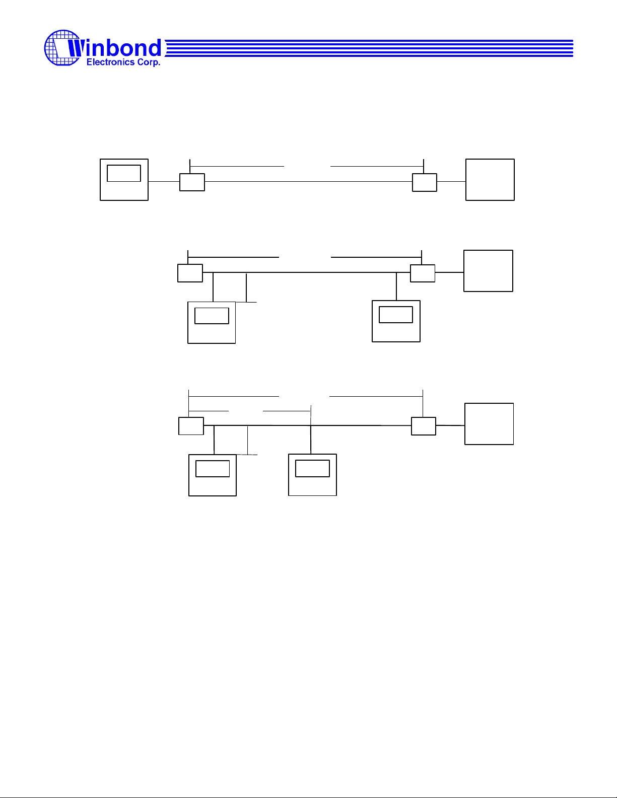
There are three wiring configurations according to I.430 : point-to-point, short passive bus and extended pass bus. They are
shown in Fig.7.2.
FIG.7.1 FRAME STRUCTURE AT S/T INTERFACE
-20 -
Publication Release Date: Sep 30, 1999
Preliminary Data Sheet
W6692 PCI ISDN S/T-Controller
W6692
TE
TR
(a) Point-to-point configuration
TR
≤ 10m
W6692
TE1
(b) Short passive bus configuration
≤ 50m
TR
≤ 10m
W6692
TE1
(c) Extended passive bus configuration
. . . . .
≤ 1000 m
100~200 m
. . . . .
100~200 m
W6692
TE8
W6692
TE8
TR
TR
TR
TR : Terminating Resistor
NT
NT
NT
FIG.7.2 W6692 WIRING CONFIGURATION IN TE APPLICATIONS
-21 -
Publication Release Date: Sep 30, 1999
Preliminary Data Sheet
SX1
18-33Ω
18-33Ω
GND
2:1
SR1
1.8kΩ
GND
8.2kΩ
8.2kΩ
2:1
W6692 PCI ISDN S/T-Controller
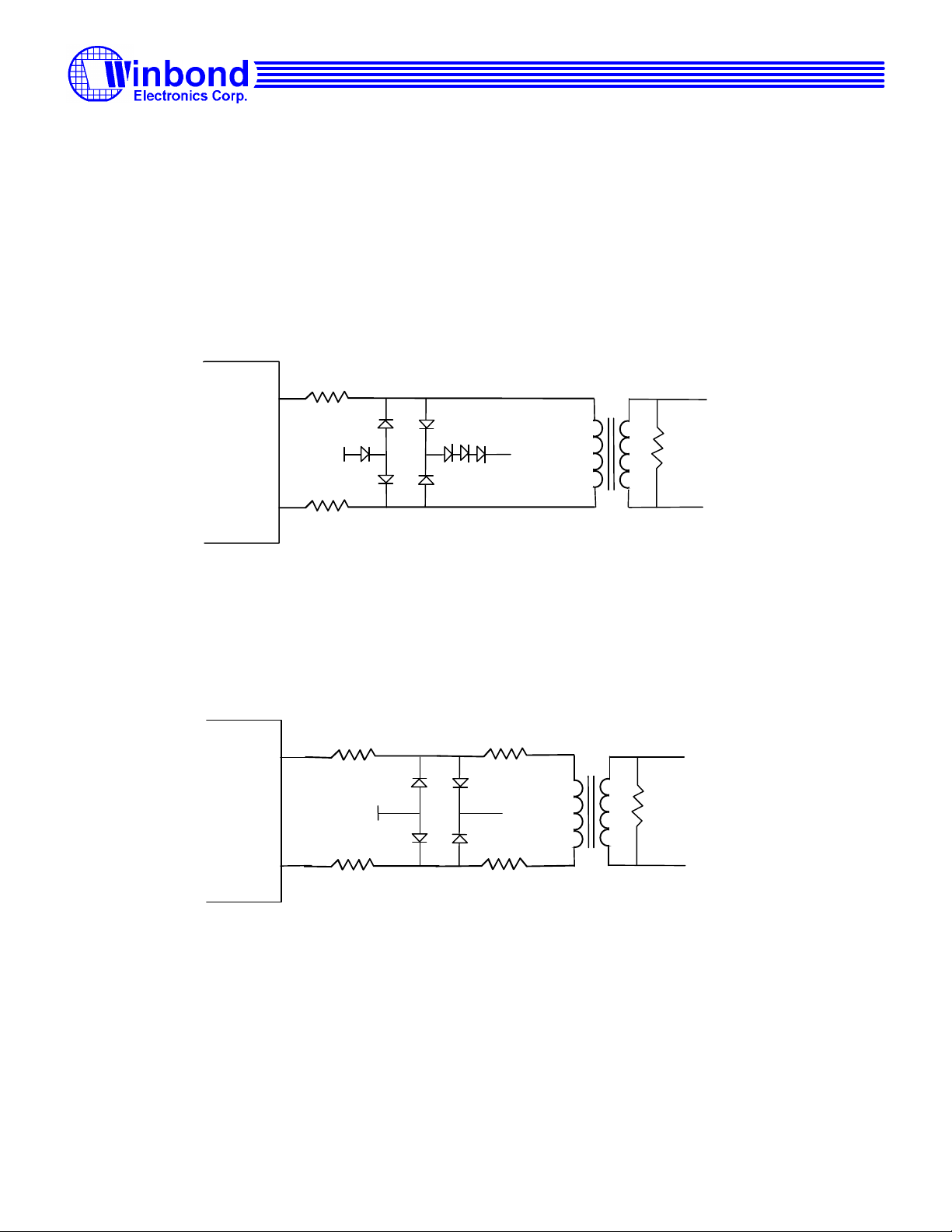
The transmitter and receiver are implemented by differential circuits to increase signal to noise ratio (SNR). The nominal
differential line pulse amplitude at 100 Ω termination is 750 mV, zero to peak. Transformers with 2:1 turn ration are needed at
transmitter and receiver for voltage level translation and DC isolation.
To meet the electrical characteristic requirements in I.430, some additional circuits are needed. At the transmitter side, the
external resistors (18 to 33 Ω) are used to adjust the output pulse amplitude and to meet the transmitter active impedance (≥ 20 Ω
when transmitting binary zeros). At the receiver side, the 1.8 kΩ resistors protect the device inputs , while the 10 kΩ resistors
(1.8 kΩ +8.2 kΩ ) limit the peak current in impedance tests. The diode bridge is used for overvoltage protection.
SX2
ο
VDD
100 Ω
FIG.7.3 EXTERNAL TRANSMITTER CIRCUITRY
SR2
1.8kΩ
ο
VDD
100 Ω
FIG.7.4 EXTERNAL RECEIVER CIRCUITRY
-22 -
Publication Release Date: Sep 30, 1999

Preliminary Data Sheet
W6692 PCI ISDN S/T-Controller
-23 -
Publication Release Date: Sep 30, 1999
Preliminary Data Sheet
W6692 PCI ISDN S/T-Controller
After hardware reset, the receiver may enter power down state in order to save power consumption. In this state, the internal
clocks are turned off, but the analog level detector is still active to detect signal coming from the S interface. The power down
state is left either by non-INFO 0 signal from S interface or C/I command from microprocessor.
7.2.2 Receiver Clock Recovery And Timing Generation
A Digital Phase Locked Loop (DPLL) circuit is used to derive the receive clock from the received data stream. This DPLL uses
a 7.68 MHz clock as reference. According to I.430, the transmit clock is normally delayed by 2 bit time from the receive clock.
The "total phase deviation from input to output" is -7% to +15% of a bit period. In some cases, delay compensation may be
needed to meet this requirement (see OPS1-0 bits in D_CTL register).
TABLE 7.1 OUTPUT PHASE DELAY COMPENSATION TABLE
OPS1 OPS0 Effect
0 0 No phase delay compensation
0 1 Phase delay compensation 260 ns
1 0 Phase delay compensation 520 ns
1 1 Phase delay compensation 1040 ns
W6692 does not need RC filter on receiver side, therefore zero delay compensation is selected normally. This is the default
setting.
The PCM output clocks (PFCK1-2, PBCK) are synchronous to the S-interface timing.
7.2.3 Layer 1 Activation/Deactivation
The layer 1 activation/deactivation procedures are implemented by a finite state machine. The state transitions are triggered by
signals received at S interface or commands issued from microprocessor. The state outputs signals to S interface and indication to
microprocessor. The CIX register is used by microprocessor to issue command, and the CIR register is used by microprocessor to
receive indication.
Some commands are used for special purposes. They are "layer 1 reset", "analog loopback", "send continuous zeros" and "send
single zero".
7.2.3.1 States Descriptions And Command/Indication Codes
F3 Deactivated without clock
This is the "deactivated" state of ITU-T I.430. The receive line awake unit is active except during a hardware reset pulse. After
reset, once the indication "1111" has been read out, internal clocks will turn off and stay at this state if INFO 0 is received on the
S line. The turn off time is approximate 93 ms. The ECK command must be issued to activate the clocks.
-24 -
Publication Release Date: Sep 30, 1999

Preliminary Data Sheet
W6692 PCI ISDN S/T-Controller
F3 Deactivated with clock
This state is identical to "F3 Deactivated without clock" except the internal clocks are enabled. The state is entered by the ECK
command. The clocks are enabled approximately 0.5 ms to 4 ms after the ECK command, depending on the crystal
capacitances. (It is about 0.5 ms for 12pF to 33pF capacitance).
F3 Awaiting Deactivation
The W6692 enters this state after receiving INFO 0 (in states F5 to F8) for 16ms (64 frames). This time constant prevents
spurious effect on S interface. Any non-INFO 0 signal on the S interface causes transition to "F5 Identifying Input" state. If this
transition does not occur in a specific time (500 - 1000 ms), the microprocessor may issue DRC or ECK command to deactivate
layer 1.
F4 Awaiting Signal
This state is reached when an activate request command has been received. In this state, the layer 1 transmits INFO1 and INFO
0 is received from the S interface. The software starts timer T3 of I.430 when issuing activate request command. The software
deactivates layer 1 if no signal other than INFO 0 has been received on S interface before expiration of T3.
F5 Identifying Input
After the receipt of any non-INFO 0 signal from NT, the W6692 ceases to transmit INFO 1 and awaits identification of INFO 2
or INFO 4. This state is reached at most 50 µs after a signal different from INFO 0 is present at the receiver of the S interface.
F6 Synchronized
When W6692 receives an activation signal (INFO 2), it responds with INFO 3 and waits for normal frames (INFO 4). This
state is reached at most 6 ms after an INFO 2 arrives at the S interface (in case the clocks were disabled in "F3 Deactivated
without clock").
F7 Activated
This is the normal active state with the layer 1 protocol activated in both directions. From state "F6 Synchronized" , state F7 is
reached at most 0.5 ms after reception of INFO 4. From state "F3 Deactivated without clock" with the clocks disabled, state F7 is
reached at most 6 ms after the W6692 is directly activated by INFO 4.
F8 Lost Framing
This is the state where the W6692 has lost frame synchronization and is awaiting resynchronization by INFO 2 or INFO 4 or
deactivation by INFO 0.
Special States:
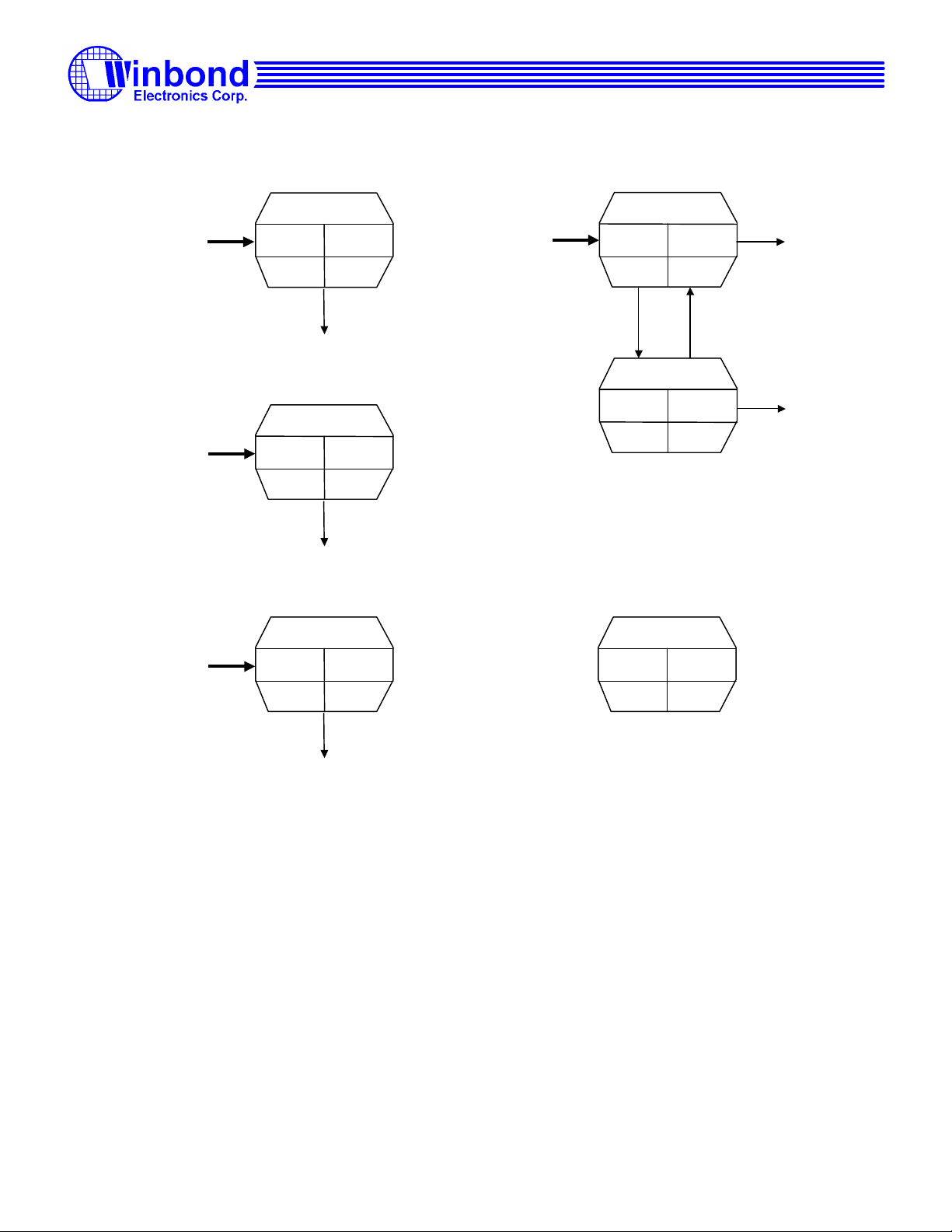
Analog Loop Initiated
On Enable Analog Loop command, INFO 3 is sent by the line transmitter internally to the line receiver (INFO 0 is sent to the
line). The receiver is not yet synchronized.
Analog Loop Activated
The receiver is synchronized on INFO 3 which is looped back internally from the transmitter. The indication 'TI" or "ATI" is
sent depending on whether or not a signal different from INFO 0 is detected on the S interface.
-25 -
Publication Release Date: Sep 30, 1999
Preliminary Data Sheet
W6692 PCI ISDN S/T-Controller
Send Continuous Pulses
A 96 kHz continuous pulse with alternating polarities is sent.
Send Single Pulses
A 2 KHz , isolated pulse with alternating polarities is sent.
Layer 1 Reset
A layer 1 reset command forces the transmission of INFO 0 and disables the S line awake detector. Thus activation from NT is
not possible. There is no indication in reset state. The reset state can be left only with ECK command.
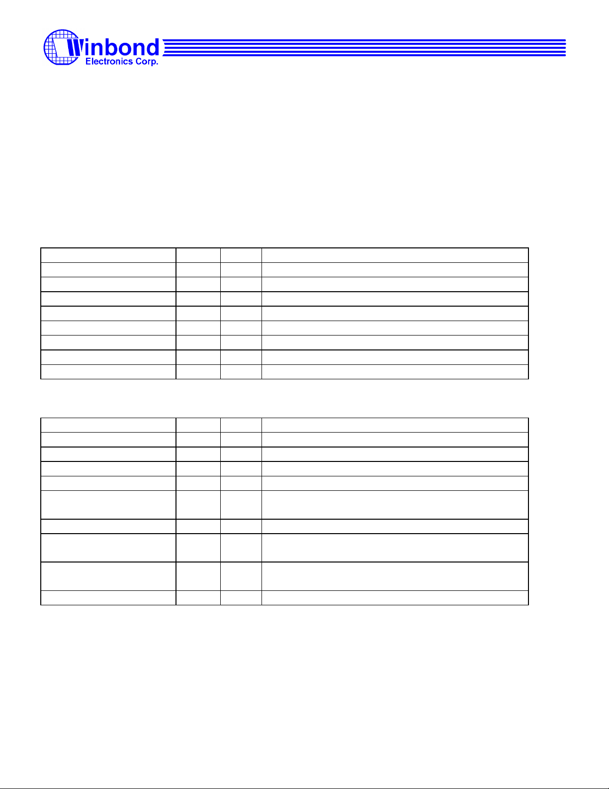
TABLE 7.2 LAYER 1 COMMAND CODES
Command Symbol Code Description
Enable clock ECK 0000 Enable internal clocks
Layer 1 reset RST 0001 Layer 1 reset
Send continuous pulses SCP 0100 Send continuous pulses at 96 kHz
Send single pulses SSP 0010 Send isolated pulses at 2 kHz
Activate request at priority 8 AR8 1000 Activate layer 1 and set D channel priority level to 8
Activate request at priority 10 AR10 1001 Activate layer 1 and set D channel priority to 10
Enable analog loopback EAL 1010 Enable analog loopback
Deactivate layer 1 DRC 1111 Deactivate layer 1 and disable internal clocks
TABLE 7.3 LAYER 1 INDICATION CODES
Indication Symbol Code Descriptions
Clock Enabled CE 0111 Internal clocks are enabled
Deactivate request downstream DRD 0000 Deactivation request by S interface, i.e INFO 0 received
Level detected LD 0100 Signal received, receiver not synchronous
Activate request downstream ARD 1000 INFO 2 received
Test indication TI 1010 Analog loopback activated or continuous zeros or single zeros
transmitted
Awake test indication ATI 1011 Level detected during test function
Activate indication with priority
class 1
Activate indication with priority
class 2
Clock disabled CD 1111 Layer 1 deactivated, internal clocks are disabled
AI8 1100 INFO 4 received, D channel priority is 8 or 9
AI10 1101 INFO 4 received, D channel priority is 10 or 11
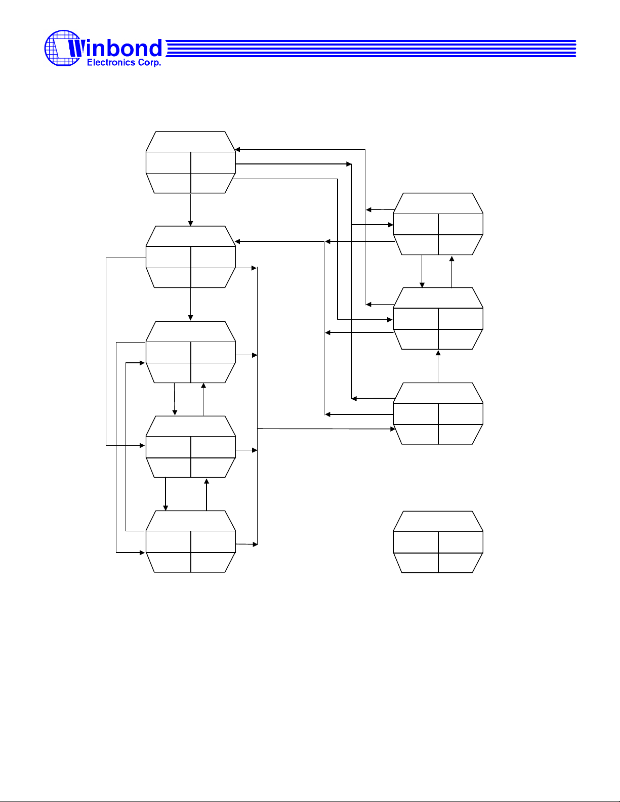
7.2.3.2 State Transition Diagrams
The followings are the state transition diagrams, which implement the activation/deactivation state matrix in I.430 (TABLE
5/I.430). The "command" and "s receive" entries in each state octagon keep the state, the "indication" and "s transmit" entries in
-26 -
Publication Release Date: Sep 30, 1999

Preliminary Data Sheet
W6692 PCI ISDN S/T-Controller
each state octagon are the state outputs. For example, at "F3 Deactivated with clock" state, the layer 1 will stay at this state if the
command is "ECK" and the INFO 0 is received on S interface. At this state, it provides "CE" indication to the microprocessor
and transmits INFO 0 on S interface. The "AR8/10" command causes transition to F4 and non-INFO 0 signal causes transition to
F5. Note that the command code writtern by the microprocessor in CIX register and indication code written by layer 1 in CIR
register are transmitted repeatedly until a new code is written.
-27 -
Publication Release Date: Sep 30, 1999
Preliminary Data Sheet
CE
i1
1)
LD
2)
i0
1)
i3
i3
1)
LD
2)
i0
CD
CE
3)
3)
3)
3)
i0
i0
i4 i2
i2
W6692 PCI ISDN S/T-Controller
i4
Lost
Framing
F4 Await. Signal
AR8/10
i0
^i0
F5 Ident. Input
^RST
any
i2
F6 Synchronized
^RST
i2
F7 Activated
AR8/10 AI8/10
i4
Lost
Framing
F8 Lost Framing
^RST
any
ARD
DRC
ECK
AR8/10
^i0
i0
AR8/10
^i0
DRC
^i0
i0
i4
Notation:
Note:
1. "^RST" means "NOT layer 1 reset command".
2. "Any" means any signal other than i0, which has not yet been
determined.
3. "^i0" means any signal other than i0.
F3 Deact w/o clk
DRC
i0
ECK
F3 Deact with clk
ECK
i0
ECK
F3 Await. Deact.
AR8/10
i0
State
com
s receive
s trans.
i0
DRC
i0
DRD
i0
Ind
FIG.7.5 LAYER 1 ACTIVATION/DEACTIVATION STATE DIAGRAM - NORMAL MODE
-28 -
Publication Release Date: Sep 30, 1999
Preliminary Data Sheet
i0
TI
3)
TI
4)
CE
5)
5)
2)
2)
2)
2)
5)
5)
W6692 PCI ISDN S/T-Controller
RST
RST
Ignored
Reset
EAL
None
ECK
SCP
Send Cont. Pulses
SCP
Ignored ic
Y
SSP
Send Sing. Pulses
SSP
Ignored is
Notation:
Y
Note :
1. RST can be issued at any state, while SCP, SCZ and EAL can be issued only at F3 or F7.
2. Y is one of the commands : ECK, DRC, RST.
3. Continuous pulses at 96 kHz.
4. Isolated pulses at 2 kHz.
5. The INFO 3 is transmitted internally only.
Ana. Loop Init.
EAL
Ignored i3
i3
Ana. Loop Act.
EAL
Ignored i3
State
com
s receive
s trans.
^i3
TI/ATI
Ind
Y
Y
FIG.7.6 LAYER 1 ACTIVATION/DEACTIVATION STATE DIAGRAM - SPECIAL MODE
-29 -
Publication Release Date: Sep 30, 1999
Preliminary Data Sheet
W6692 PCI ISDN S/T-Controller
7.2.4 D Channel Access Control
The D channel access control includes collision detection and priority management. The collision detection is always enabled.
The priority management procedure as specified in ITU-T I.430 is fully implemented in W6692.
A collision is detected if the transmitted D bit and the received echo bit do not match. When this occurs, D channel
transmission is immediately stopped and the echo channel is monitored to attempt the next D channel access. The layer 1 module
uses an internal signal to inform layer 2 module of the collision condition (DRDY bit goes inactive in D_XSTA register).
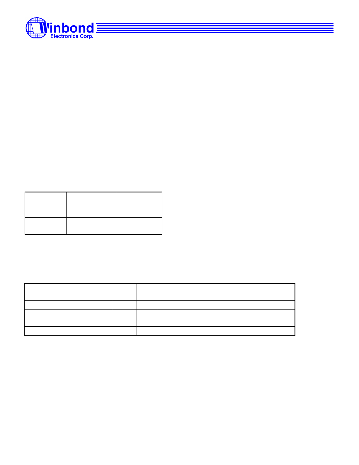
There are two priority classes: class 1 and class 2. Within each class, there are normal and lower priority levels.
TABLE 7.4 D PRIORITY CLASSES
Normal level Lower level
Priority class
1
Priority class
2
The selection of priority class is via the AR8/AR10 command. The following table summarizes the commands/indications used
for setting the priority classes:
8 9
10 11
TABLE 7.5 D PRIORITY COMMANDS/INDICATIONS
Command Symbol Code Remarks
Activate request, set priority 8 AR8 1000 Activation command, set D channel priority to 8
Activate request, set priority 10 AR10 1001 Activation command, set D channel priority to 10
Indication Abbr. Remarks
Activate indication with priority 8 AI8 1100 Info 4 received, D channel priority is 8 or 9
Activate indication with priority 10 AI10 1101 Info 4 received, D channel priority is 10 or 11
7.2.5 Frame Alignment
-30 -
Publication Release Date: Sep 30, 1999
 Loading...