

Winbond Electronics W49L102Q-90B, W49L102Q-90, W49L102Q-70B, W49L102Q-70 Datasheet

Preliminary W49L102
64K × 16 CMOS 3.3V FLASH MEMORY
GENERAL DESCRIPTION
The W49L102 is a 1-megabit, 3.3-volt only CMOS flash memory organized as 64K × 16 bits. The
device can be programmed and erased in-system with a standard 3.3V power supply. A 12-volt VPP is
not required. The unique cell architecture of the W49L102 results in fast program/erase operations
with extremely low current consumption (compared to other comparable 3.3-volt flash memory
products). The device can also be programmed and erased using standard EPROM programmers.
FEATURES
• Single 3.3-volt operations:
− 3.3-volt Read
− 3.3-volt Erase
− 3.3-volt Program
• Fast Program operation:
− Word-by-Word programming: 50 µS (max.)
• Fast Erase operation: 100 mS (typ.)
• Fast Read access time: 55/70/90 nS
• Endurance: 1K/10K cycles (typ.)
• Twenty-year data retention
• Hardware data protection
• 8K word Boot Block with Lockout protection
• Low power consumption
− Active current: 15 mA (typ.)
− Standby current: 10 µA (typ.)
• Automatic program and erase timing with
internal VPP generation
• End of program or erase detection
− Toggle bit
− Data polling
• Latched address and data
• TTL compatible I/O
• JEDEC standard word-wide pinouts
• Available packages: 40-pin TSOP and 44-pin
PLCC
Publication Release Date: June 1999
- 1 - Revision A1
Preliminary W49L102
CE
OE
WE
PIN CONFIGURATIONS
A9
A10
A11
A12
A13
A14
A15
NC
WE
V
NC
CE
DQ15
DQ14
DQ13
DQ12
DQ11
DQ10
DQ9
DQ8
DQ12
DQ11
DQ10
DD
DQ9
DQ8
GND
DQ7
DQ6
DQ5
DQ4
1
2
3
4
5
6
7
8
9
10
11
12
13
14
15
16
17
18
19
20
D
Q
13
7
8
9
10
11
12
13
NC
14
15
16
17
18
D
Q
3
40-pin
TSOP
D
Q
Q
15
14
56
4
D
N
C
N
D
C
C
E
441
2
3
V
/
D
44-pin
PLCC
2322
20
21
19
D
Q
2
NCA
D
/
D
Q
O
0
Q
1
E
0
W
E
43
A1A
BLOCK DIAGRAM
V
DD
V
40
GND
A8
39
A7
38
A6
37
A5
36
A4
35
A3
34
A2
33
A1
32
A0
31
30
OE
29
DQ0
28
DQ1
27
DQ2
26
DQ3
25
DQ4
DQ5
24
DQ6
23
DQ7
22
GND
21
A
A
/
1
1
N
4
5
C
4041
42
39
A13
38
A12
37
A11
36
A10
35
A9
34
GND
33
NC
32
A8
31
A7
30
A6
A5
29
27
262524
28
A3A
4
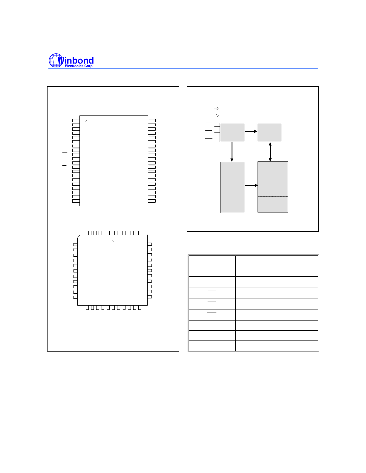
2
PIN DESCRIPTION
SS
CE
OE
CONTROL
OUTPUT
BUFFER
WE
A0
.
.
A15
DECODER
MAIN
MEMORY
(56K Words)
BootBlock
(8K Words)
SYMBOL PIN NAME
A0−A15
DQ0−DQ15
Address Inputs
Data Inputs/Outputs
Chip Enable
Output Enable
Write Enable
VDD Power Supply
DQ0
.
.
DQ15
GND Ground
NC No Connection
- 2 -

Preliminary W49L102
WE
FUNCTIONAL DESCRIPTION
Read Mode
The read operation of the W49L102 is controlled by CE and OE, both of which have to be low for the
host to obtain data from the outputs. CE is used for device selection. When CE is high, the chip is
de-selected and only standby power will be consumed. OE is the output control and is used to gate
data from the output pins. The data bus is in high impedance state when either CE or OE is high.
Refer to the timing waveforms for further details.
Boot Block Operation
There is one 8K-word boot block in this device, which can be used to store boot code. It is located in
the first 8K words of the memory with the address range from 0000 hex to 1FFF hex.
See Command Codes for Boot Block Lockout Enable for the specific code. Once this feature is set
the data for the designated block can not be erased or programmed (programming lockout); other
memory locations can be changed by the regular programming method. Once the boot block
programming lockout feature is activated, the chip erase function will only affect the main memory.
In order to detect whether the boot block feature is set on the 8K-words block, users can perform
software command sequence: enter the product identification mode (see Command Codes for
Identification/Boot Block Lockout Detection for specific code), and then read from address "0002
hex". If the output data is "FF hex," the boot block programming lockout feature is activated; if the
output data is "FE hex," the lockout feature is inactivated and the block can be erased/programmed.
To return to normal operation, perform a three-byte command sequence (or an alternate single-word
command) to exit the identification mode. For the specific code, see Command Codes for
Identification/Boot Block Lockout Detection.
Input Levels
While operating with a 3.0V−3.6V power supply, the address inputs and control inputs (OE, CE and
) may be driven from 0 to 5.5V without adversely affecting the operation of the device. The I/O
lines can only be driven from 0 to 3.6V.
Chip Erase Operation
The chip-erase mode can be initiated by a six-word command sequence. After the command loading
cycle, the device enters the internal chip erase mode, which is automatically timed and will be
completed in a fast 100 mS (typical). The host system is not required to provide any control or timing
during this operation. If the boot block programming lockout is activated, only the data in the main
memory will be erased to FF(hex), and the data in the boot block will not be erased (remains same as
before the chip erase operation). The entire memory array (main memory and boot block) will be
erased to FF hex. by the chip erase operation if the boot block programming lockout feature is not
activated. The device will automatically return to normal read mode after the erase operation
completed. Data polling and/or Toggle Bits can be used to detect end of erase cycle.
Main Memory Erase Operation
The main memory erase mode can be initiated by a six-word command sequence. After the
command loading cycle, the device enters the internal main-memory erase mode, which is
automatically timed and will be completed in a fast 100 mS (typical). The host system is not required
Publication Release Date: June 1999
- 3 - Revision A1

Preliminary W49L102
WE
to provide any control or timing during this operation. The device will automatically return to normal
read mode after the erase operation completed. Data polling and/or Toggle Bits can be used to detect
end of erase cycle.
Program Operation
The W49L102 is programmed on a word-by-word basis. Program operation can only change logical
data "1" to logical data "0" The erase operation (changed entire data in main memory and/or boot
block from "0" to "1" is needed before programming.
The program operation is initiated by a 4-word command cycle (see Command Codes for Word
Programming). The device will interally enter the program operation immediately after the wordprogram command is entered. The internal program timer will automatically time-out (50 µS max. TBP) once completed and return to normal read mode. Data polling and/or Toggle Bits can be used to
detect end of program cycle.
Hardware Data Protection
The integrity of the data stored in the W49L102 is also hardware protected in the following ways:
(1) Noise/Glitch Protection: A WE pulse of less than 15 nS in duration will not initiate a write cycle.
(2) VDD Power Up/Down Detection: The programming operation is inhibited when VDD is less than
1.8V typical.
(3) Write Inhibit Mode: Forcing OE low, CE high, or WE high will inhibit the write operation. This
prevents inadvertent writes during power-up or power-down periods.
(4) VDD power-on delay: When VDD has reached its sense level, the device will automatically time-
out 10 mS before any write (erase/program) operation.
Data Polling (DQ7 & DQ15)- Write Status Detection
The W49L102 includes a data polling feature to indicate the end of a program or erase cycle. When
the W49L102 is in the internal program or erase cycle, any attempt to read DQ7 or DQ15 of the last
word loaded will receive the complement of the true data. Once the program or erase cycle is
completed, DQ7 or DQ15 will show the true data. Note that DQ7 or DQ15 will show logical "0" during
the erase cycle, and become logical "1" or true data when the erase cycle has been completed.
Toggle Bit (DQ6 & DQ14)- Write Status Detection
In addition to data polling, the W49L102 provides another method for determining the end of a
program cycle. During the internal program or erase cycle, any consecutive attempts to read DQ6 or
DQ14 will produce alternating 0's and 1's. When the program or erase cycle is completed, this toggling
between 0's and 1's will stop. The device is then ready for the next operation.
Product Identification
The product ID operation outputs the manufacturer code and device code. Programming equipment
automatically matches the device with its proper erase and programming algorithms.
The manufacturer and device codes can be accessed by software or hardware operation. In the
software access mode, a six-word (or JEDEC 3-word) command sequence can be used to access the
product ID. A read from address 0000H outputs the manufacturer code (00DAh). A read from address
0001H outputs the device code (00BFh). The product ID operation can be terminated by a three-word
command sequence or an altenate one-word command sequence (see Command Definition table).
In the hardware access mode, access to the product ID is activated by forcing CE and OE low,
high, and raising A9 to 12 volts.
- 4 -
Preliminary W49L102
CEOEWE
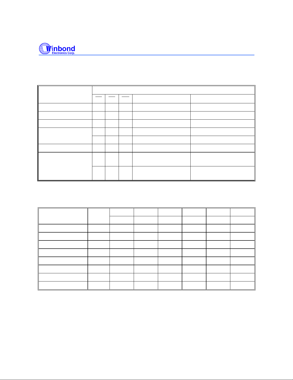
TABLE OF OPERATING MODES
Operating Mode Selection
(VHH = 12V ± 0.5V )
MODE PINS
ADDRESS DQ.
Read VIL VIL VIH AIN Dout
Write VIL VIH VIL AIN Din
Standby VIH X X X High Z
Write Inhibit X VIL X X High Z/DOUT
X X VIH X High Z/DOUT
Output Disable X VIH X X High Z
Product ID VIL VIL VIH
VIL VIL VIH
A0 = VIL; A1−A15 = VIL;
A9 = VHH
A0 = VIH; A1−A15 = VIL;
A9 = VHH
Manufacturer Code
00DA (Hex)
Device Code
00BF (Hex)
TABLE OF COMMAND DEFINITION
Command No. of 1st Cycle 2nd Cycle 3rd Cycle 4th Cycle 5th Cycle 6th Cycle
Description Cycles
Read 1
Chip Erase 6
Main Memory Erase 6
Word Program 4
Boot Block Lockout 6
Product ID Entry 3
Product ID Exit
Product ID Exit
Note: Address Format: A14−A0 (Hex); Data Format: DQ15−DQ8 (Don't Care); DQ7-DQ0 (Hex)
Either one of the two Product ID Exit commands can be used.
(1)
(1)
Addr. Data Addr. Data Addr. Data Addr. Data Addr. Data Addr. Data
AIN D
OUT
5555 AA 2AAA 55 5555 80 5555 AA 2AAA 55 5555 10
5555 AA 2AAA 55 5555 80 5555 AA 2AAA 55 5555 30
5555 AA 2AAA 55 5555 A0 AIN D
5555 AA 2AAA 55 5555 80 5555 AA 2AAA 55 5555 40
5555 AA 2AAA 55 5555 90
3
1
5555 AA 2AAA 55 5555 F0
XXXX F0
IN
Publication Release Date: June 1999
- 5 - Revision A1
Preliminary W49L102
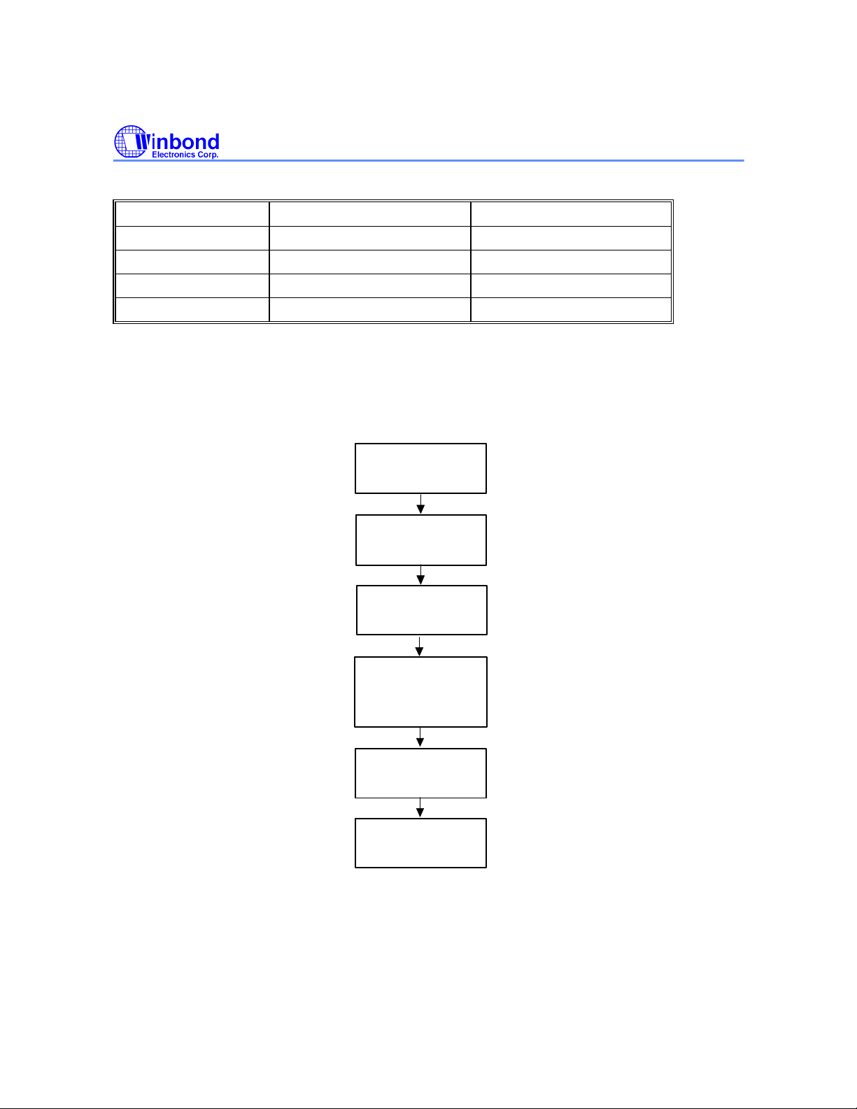
Command Flow
Command Codes for Word Program
WORD SEQUENCE ADDRESS DATA
0 Write 5555H AAH
1 Write 2AAAH 55H
2 Write 5555H A0H
3 Write Programmed-Address Programmed-Data
Word Program Flow Chart
Word Program
Load data AA
address 2AAA
Load data A0
address 5555
to
address 5555
Load data 55
to
to
Load data Din
to
programmed-
address
Pause 50 S
µ
Exit
Notes for software program code:
Data Format: DQ15−DQ0 (Hex); XX = Don't Care
Address Format: A14−A0 (Hex)
- 6 -
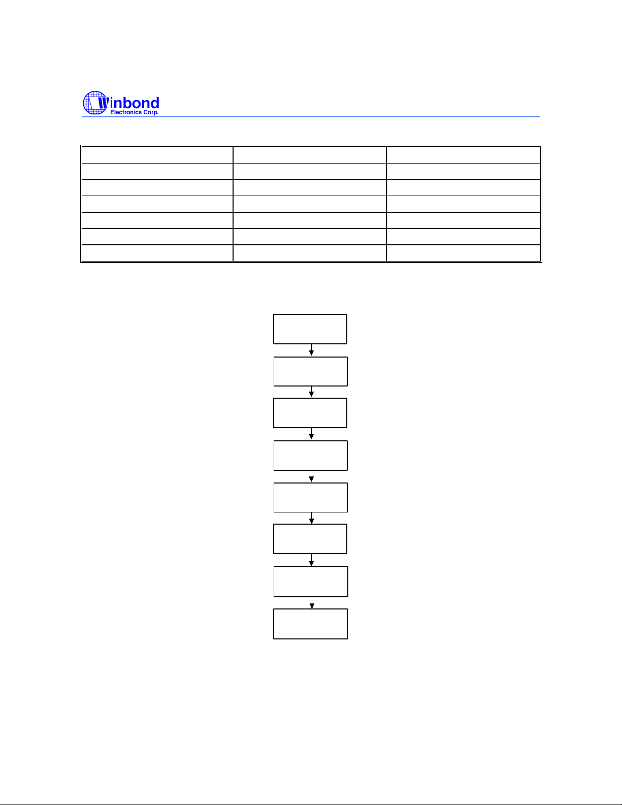
Command Codes for Chip Erase
BYTE SEQUENCE ADDRESS DATA
1 Write 5555H AAH
2 Write 2AAAH 55H
3 Write 5555H 80H
4 Write 5555H AAH
5 Write 2AAAH 55H
6 Write 5555H 10H
Chip Erase Acquisition Flow
Load data AA
to
address 5555
Load data 55
to
address 2AAA
Preliminary W49L102
Notes for chip erase:
Data Format: DQ15-DQ8: Don't Care; DQ7−DQ0 (Hex)
Address Format: A14−A0 (Hex)
Load data 80
to
address 5555
Load data AA
to
address 5555
Load data 55
to
address 2AAA
Load data 10
to
address 5555
Pause 1 Sec.
Exit
Publication Release Date: June 1999
- 7 - Revision A1
 Loading...