

White Electronic Designs EDI8L32128V20AI, EDI8L32128V20AC, EDI8L32128V15AI, EDI8L32128V15AC, EDI8L32128V12AI Datasheet
...
Features
128Kx32 bit CMOS Static
Analog SHARC
• ADSP-21060L
• ADSP-21062L
Random Access Memory Array
• Fast Access Times: 12,15 and 20ns
• User Configurable Organization
• Master Output Enable and Write Control
• TTL Compatible Inputs and Outputs
• Fully Static, No Clocks
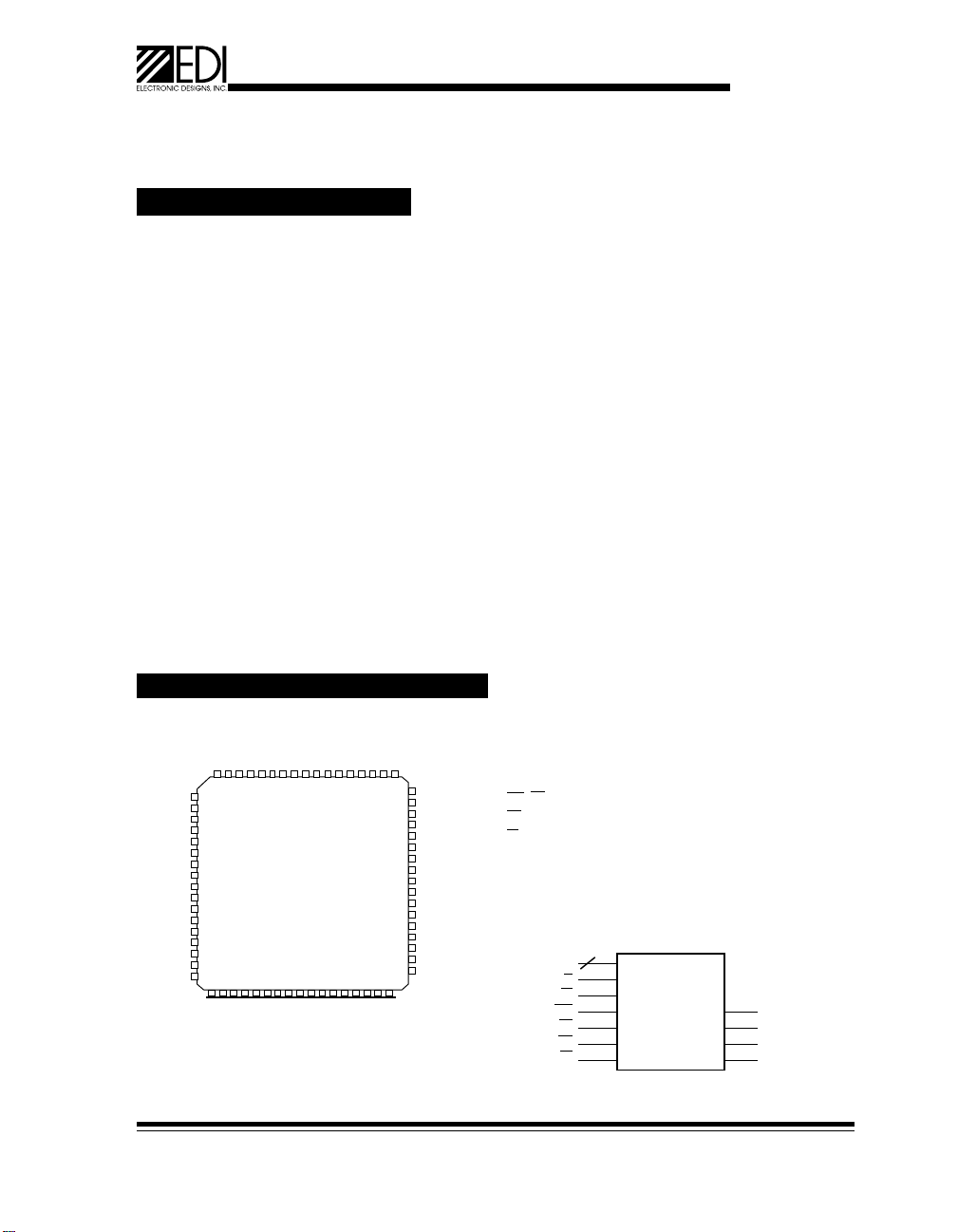
Surface Mount Package
• 68 Lead PLCC, No. 99 (JEDEC MO-47AE)
• Small Footprint, 0.990 Sq. In.
• Multiple Ground Pins for Maximum
Single 3.3V (±5%) Supply Operation
TM
External Memory Solution
with Minimal Additional Logic
Noise Immunity
EDI8L32128V
128Kx32 SRAM 3.3 Volt
128Kx32 CMOS High Speed
Static RAM
The EDI8L32128V is a high speed, 3.3 volt, four megabit
density Static RAM. The device is available with access
times of 12, 15 and 20ns, allowing the device to support
60MHz DSPs with no wait states. The high speed, 3.3V
supply voltage and byte configurability make the device
ideal for interfacing with Analog Devices ADSP-21062L or
ADSP-21060L SHARC DSPs.
The device can be configured as a 128Kx32 and used to
create a single chip external data memory solution for the
SHARC (figure 1). Providing a 51% space savings when
compared to four 128Kx8, 400mil wide plastic SOJs. the
EDI8L32128V has a 10pf load on the data lines vs. 24pf for
four plastic SOJs. Memory upgrades in the same footprint
can be accomplished with the EDI8L32256V (256Kx32) or
the EDI8L32512V (512KX32). This is covered in detail in the
application report "The EDI's x32 MCM-L SRAM Family:
Integrated Memory Solution for the Analog SHARC DSP"
Alternatively the device's chip enables can configure it as a
256Kx16. A 256Kx48 program memory array for the
SHARC is created using three devices (figure 2). If this
memory is too deep, two 128Kx24's (EDI8L24128V) can be
used to create a 128Kx48 memory array.
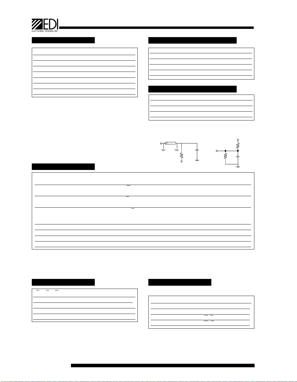
Pin Configurations and Block Diagram
9 DQ16
8NC
7NC
6E3\
5E2\
4E1\
3EØ\
2NC
1VCC
68 NC
67 NC
66 G\
65 W\
64 A16
63 A15
62 A14
61 DQ15
DQ14
DQ17
10
DQ18
11
DQ19
12
VSS
13
DQ20
14
DQ21
15
DQ22
16
DQ23
17
VCC
18
DQ24
19
DQ25
20
DQ26
21
DQ27
22
VSS
23
DQ28
24
DQ29
25
DQ30
26
A6 28
A5 29
A4 30
A3 31
A2 32
A1 33
DQ31 27
Note: Pin 2 & 67 on the 64Kx32 (EDI8L3265C) and the 256Kx32 (EDI8L32256C)
are word select pins.
AØ 34
• One Research Drive • Westborough, MA 01581 USA • 508-366-5151 • FAX 508-836-4850 •
A9 40
A13 36
A12 37
A11 38
A10 39
VCC 35
60
DQ13
59
DQ12
58
VSS
57
DQ11
56
DQ10
55
DQ9
54
DQ8
53
VCC
52
DQ7
51
DQ6
50
DQ5
49
DQ4
48
VSS
47
DQ3
46
DQ2
45
DQ1
44
A8 41
A7 42
DQØ 43
Electronic Designs Incorporated
http://www.electronic-designs.com
EDI8L32128V Rev. 1 4/97 ECO #8366
Note: Solder Reflow temperature should not exceed 260°C for 10 seconds
Pin Names
AØ-A16 Address Inputs
EØ-E3 Chip Enables (One per Byte)
W Master Write Enable
G Master Output Enable
DQØ-DQ31 Common Data Input/Output
VCC Power (+3.3V±10%)
VSS Ground
NC No Connection
AØ-A16
17
G
W
EØ
E1
E2
E3
1
128Kx32
Memory
Array
DQØ-DQ7
DQ8-DQ15
DQ16-DQ23
DQ24-DQ31
Absolute Maximum Ratings*
Voltage on any pin relative to VSS -0.5V to 4.6V
Operating Temperature TA (Ambient)
Commercial 0°C to + 70°C
Industrial -40°C to +85°C
Storage Temperature -55°C to +125°C
Recommended DC Operating Conditions
Parameter Sym Min Typ Max Units
Supply Voltage VCC 3.135V 3.3 3.465V V
Supply Voltage VSS 0 0 0 V
Input High Voltage VIH 2.2 -- VCC+0.3 V
Input Low Voltage VIL -0.3 -- 0.8 V
Power Dissipation 3 Watts
Output Current. 20 mA
Junction Temperature, TJ 175°C
AC Test Conditions
Input Pulse Levels VSS to 3.0V
*Stress greater than those listed under "Absolute Maximum Ratings" may cause
permanent damage to the device. This is a stress rating only and functional
operation of the device at these or any other conditions greater than those indicated
in the operational sections of this specification is not implied. Exposure to absolute
maximum rating conditions for extended periods may affect reliability.
DC Electrical Characteristics
Input Rise and Fall Times 5ns
Input and Output Timing Levels 1.5V
Output Load Figure 1
(note: For TEHQZ,TGHQZ and TWLQZ, CL = 5pF) (see figure 2)
Figure 1 Figure 2
Z0 = 50 Ω
Q
65 pF
RL = 50 Ω
VL = 1.5V
Dout
353 Ω
Parameter Sym Conditions Min Max Units
12 15 20 ns
Operating Power Supply Current ICC1 W= VIL, II/O = 0mA, 680 660 620 mA
Min Cycle
Standby (TTL) Supply Current ICC2 E • VIH, VIN- VIL or 120 120 120 mA
VIN • VIH, f=ØMHz
Full Standby CMOS ICC3 E • VCC-0.2V 40 40 40 mA
Supply Current VIN • VCC-0.2V or
VIN - 0.2V
Input Leakage Current ILI VIN = 0V to VCC ±10 µA
Output Leakage Current ILO V I/O = 0V to VCC ±10 µA
Output High Volltage VOH IOH = -4.0mA 2.4 V
Output Low Voltage VOL IOL = 8.0mA 0.4 V
VCC
319 Ω
5 pF
Typical: TA = 25°C, VCC = 3.3V
Truth Table
G E W Mode Output Power
X H X Standby High Z
H L H Output Deselect High Z ICC1
L L H Read DOUT ICC1
X L L Write DIN ICC1
EDI8L32128V
128Kx32 SRAM 3.3 Volt
ICC2,ICC3
EDI8L32128V Rev. 1 4/97 ECO #8366
Capacitance
(f=1.0MHz, VIN=VCC or VSS)
Parameter Sym Max Unit
Address Lines CA 40 pF
Data Lines CD/Q 10 pF
Write & Output Enable Lines
Chip Enable Lines EØ-E3 8 pF
These parameters are sampled, not 100% tested.
2
W, G 40 pF
 Loading...