

White Electronic Designs EDI8L32128C25AC, EDI8L32128C20AI, EDI8L32128C20AC, EDI8L32128C17AI, EDI8L32128C17AC Datasheet
...
1
White Electronic Designs Corporation (508) 366-5151 www.whiteedc.com
White Electronic Designs
EDI8L32128C
N
O
T
R
E
C
O
M
M
E
N
D
E
D
F
O
R
N
E
W
D
E
S
IG
N
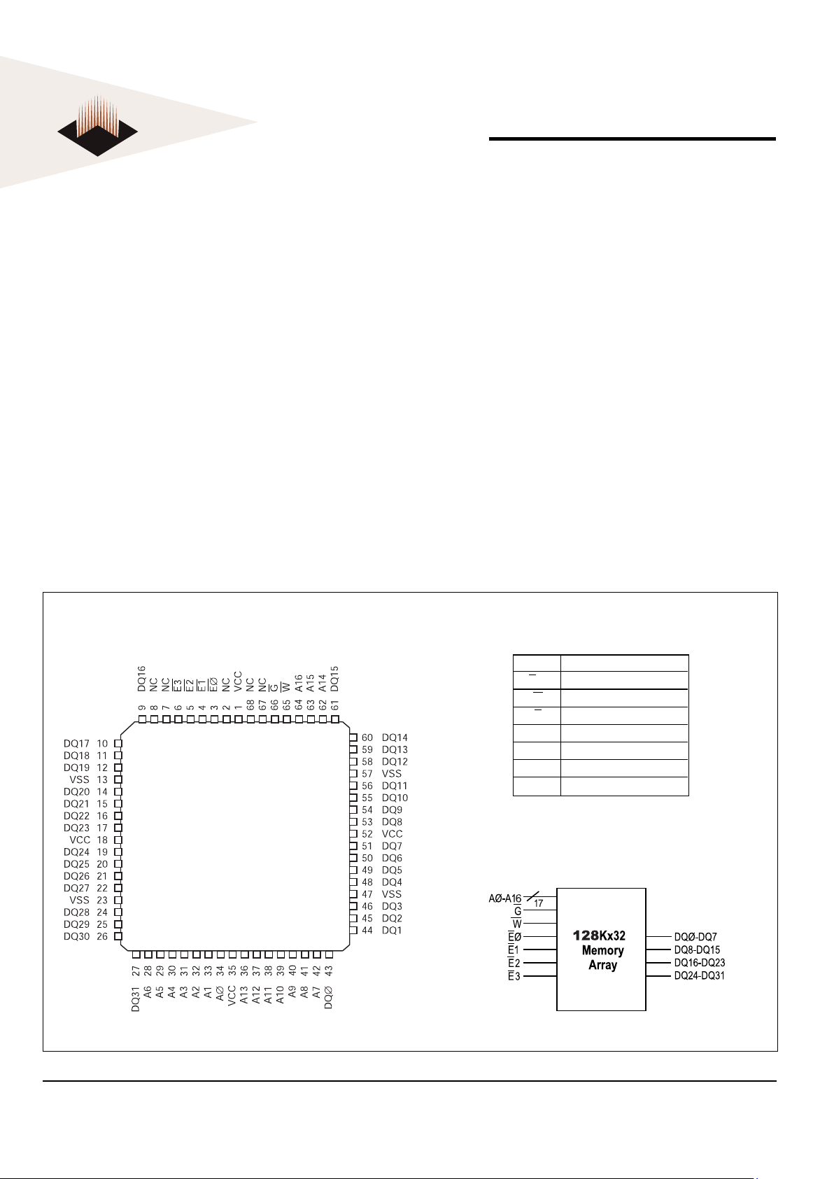
128Kx32 CMOS High Speed Static RAM
FEATURES
n 128Kx32 bit CMOS Static
n Random Access Memory Array
Fast Access Times: 12, 15, 17, 20, and 25ns
Individual Byte Enables
User Configurable Organization with Minimal
Additional Logic
Master Output Enable and Write Control
TTL Compatible Inputs and Outputs
Fully Static, No Clocks
n Surface Mount Package
68 Lead PLCC, No. 99 (JEDEC MO-47AE)
Small Footprint, 0.990 Sq. In.
Multiple Ground Pins for Maximum Noise
Immunity
n Single +5V (±5%) Supply Operation
DESCRIPTION
The EDI8L32128C is a high speed, high performance,
four megabit density Static RAM organized as a
128Kx32 bit array.
Four Chip Enables, Write Control, and Output Enable
provide the user with a flexible memory solution. The
user may independently enable each of the four bytes,
and, with minimal additional peripheral logic, the unit
may be configured as a 256Kx16 or 512Kx8 array.
Fully asynchronous circuitry is used, requiring no clocks
or refreshing for operation and providing equal access
and cycle times for ease of use.
The EDI8L32128C, allows 4 megabits of memory to
be placed in less than 0.990 square inches of board
space; a savings of 0.885 square inches over four
standard 128Kx8 components.
NOTE: Solder Reflow temperature should not exceed 230°C
NOTE: Pin 2 & 67 on the 64Kx32 (EDI8L3265C) and the 256Kx32 (EDI8L32256C) are word select pins.
BLOCK DIAGRAM
F I G . 1 PIN CONFIGURATION
PIN DESCRIPTION
AØ-16 Address Inputs
EØ-3 Chip Enables (One per Byte)
W Master Write Enable
G Master Output Enable
DQØ-31 Common Data Input/Output
VCC Power (+5V±5%)
VSS Ground
NC No Connection
TOP VIEW
August 2002 Rev. 6
ECO #15423
White Electronic Designs Corporation (508) 366-5151 www.whiteedc.com
2
White Electronic Designs
EDI8L32128C
ABSOLUTE MAXIMUM RATINGS* RECOMMENDED DC OPERATING CONDITIONS
*Stress greater than those listed under "Absolute Maximum Ratings"
may cause permanent damage to the device. This is a stress rating
only and functional operation of the device at these or any other
conditions greater than those indicated in the operational sections of
this specification is not implied. Exposure to absolute maximum
rating conditions for extended periods may affect reliability.
CAPACITANCE
(f = 1.0MHz, VIN = VCC or VSS)
AC TEST CONDITIONS
DC ELECTRICAL CHARACTERISTICS
Voltage on any pin relative to VSS -0.5V to 7.0V
Operating Temperature TA (Ambient)
Commercial 0°C to + 70°C
Industrial -40°C to +85°C
Storage Temperature -55°C to +125°C
Power Dissipation 4 Watts
Output Current. 20 mA
Junction Temperature, TJ 175°C
Parameter Sym Min Typ Max Units
Supply Voltage VCC 4.75 5.0 5.25 V
Supply Voltage VSS 000V
Input High Voltage VIH 2.2 -- VCC+0.5 V
Input Low Voltage V
IL -0.3 -- 0.8 V
Parameter Sym Max Unit
Address Lines CA 40 pF
Data Lines CD/Q 10 pF
Write & Output Enable Lines W, G 40 pF
Chip Enable Lines/Byte Select E0-3 8pF
TRUTH TABLE
E W G Mode Output Power
H X X Standby High Z ICC2,ICC3,
L H H Output Disable High Z ICC1
L X X Output Disable High Z ICC1
L H L Read DOUT ICC1
L L X Write DIN ICC1
Parameter Sym Conditions Typ Max Units
12* 15 17 20/25
Operating Power Supply Current ICC1 W= VIL, II/O = 0mA, 620 720 680 640 600 m A
Min Cycle
Standby (TTL) Supply Current ICC2 E VIH, VIN VIL or 160 160 160 160 m A
VIN VIH, f = ØMHz
Full Standby CMOS Supply Current ICC3 E VCC -0.2V
20
VIN VCC -0.2V or 20 20 20 mA
VIN 0.2V
Input Leakage Current ILI VIN = 0V to VCC ±10 µA
Output Leakage Current ILO V I/O = 0V to VCC ±10 µA
Output High Volltage VOH IOH = -4.0mA 2.4 V
Output Low Voltage VOL IOL = 8.0mA 0.4 V
Input Pulse Levels VSS to 3.0V
Input Rise and Fall Times 5ns
Input and Output Timing Levels 1.5V
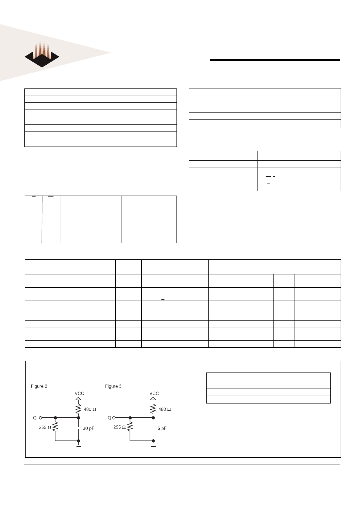
Output Load Figure 2
NOTE: For tEHQZ, tGHQZ and tWLQZ, CL = 5pF Figure 3)
Typical: TA = 25°C, VCC = 5.0V
 Loading...