

White Electronic Designs EDI8L24129V15BC, EDI8L24129V12BI, EDI8L24129V12BC, EDI8L24129V10BC, EDI8L24129V15BI Datasheet
White Electronic Designs
128Kx24 SRAM 3.3 Volt
EDI8L24129V
FEATURES
128Kx24 bit CMOS Static
Random Access Memory Array
< Fast Access Times: 10, 12, and 15ns
< Master Output Enable and Write Control
< TTL Compatible Inputs and Outputs
< Fully Static, No Clocks
Surface Mount Package
< 119 Lead BGA (JEDEC MO-163), No. 391
< Small Footprint, 14mm x 22mm
< Multiple Ground Pins for Maximum
Noise Immunity
Single +3.3V (±5%) Supply Operation
DSP Memory Solution
< Motorola DSP5630xTM
< Analog Devices SHARCTM
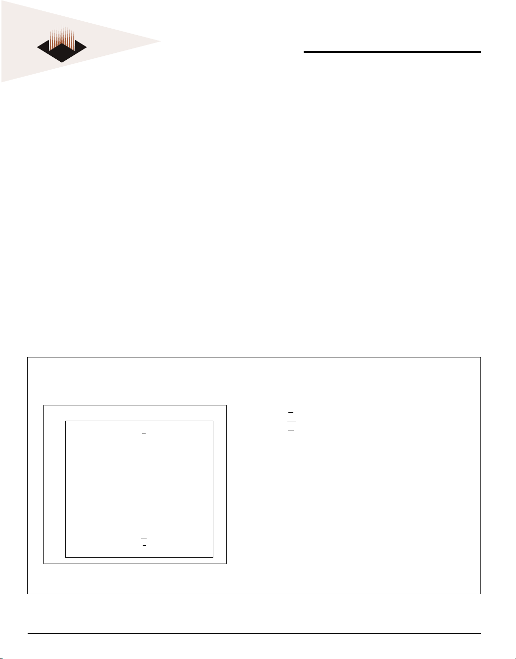
PIN CONFIGURATION
Pin Symbols
The EDI8L24129VxxBC is a 3.3V, three megabit SRAM
constructed with three 128Kx8 die mounted on a multilayer laminate substrate. With 10 to 15ns access times,
x24 width and a 3.3V operating voltage, the
EDI8L24129V is ideal for creating a single chip memory
solution for the Motorola DSP5630x (Figure 3) or a two
chip solution for the Analog Devices SHARCTM DSP
(Figure 4).
The single or dual chip memory solutions offer improved
system performance by reducing the length of board
traces and the number of board connections compared
to using multiple monolithic devices. For example, the
capacitance load on the data lines for the BGA package
is 58% less than a monolithic SOJ solution.
The JEDEC Standard 119 lead BGA provides a 44%
space savings over using 128Kx8, 300mil wide SOJs
and the BGA package has a maximum height of 100
mils compared to 148 mils for the SOJ packages. The
BGA package also allows the use of the same manufacturing and inspection techniques as the Motorola
DSP, which is also in a BGA package.
Pin Names
1234567
ANCAOA1A2A3A4NC
B NC A5 A6 E A7 A8 NC
C I/012 NC NC NC NC NC I/00
D I/0 13 VC C GND GND GND VCC I/01
E I / 014 GND VCC GND VCC GND I/02
F I/0 15 VC C GND GND GND VCC I/03
G I/016 GND VC C GND VCC GND I/04
H I/0 17 VC C GND GND GND VCC I/05
I NC GND V CC GND VCC GND NC
J I/018 V CC GND GND GND V C C I/06
K I / 019 GND VCC GND VCC GND I/07
L I /020 V CC GND GND GND VC C I/08
M I/021 GND VCC GND VCC GND I/09
N I/022 VCC GND GND GND VCC I/010
O I/023 NC NC NC NC NC I/011
PNCA9A10WA11A12NC
Q NC A13 A14 G A15 A16 NC
July 2002 Rev 3
ECO #14690
AØ-A16 Address Inputs
E Chip Enable
W Master Write Enable
G Master Output Enable
DQØ-DQ23 Common Data Input/Output
VCC Power (3.3V±5%)
GND Ground
NC No Connection
1 White Electronic Designs Corporation (508) 366-5151 www.whiteedc.com
White Electronic Designs
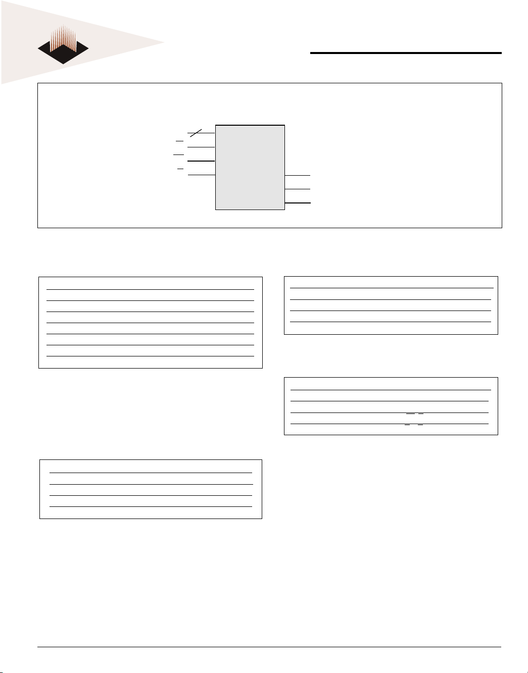
BLOCK DIAGRAM
A0-A
16
G
W
EDI8L24129V
17
128K x 24
E
Memory
Array
0
-DQ
DQ
DQ8-DQ
DQ16-DQ
7
15
23
ABSOLUTE MAXIMUM RATINGS
Voltage on any pin relative to VSS -0.5V to 4.6V
Operating Temperature TA (Ambient)
Commercial 0°C to + 70°C
Industrial -40°C to +85°C
Storage Temperature -55°C to +125°C
Power Dissipation 1.5 Watts
Output Current. 50 mA
Junction Temperature, TJ 175°C
*Stress greater than those listed under "Absolute Maximum Ratings"
may cause permanent damage to the device. This is a stress rating
only and functional operation of the device at these or any other
conditions greater than those indicated in the operational sections of
this specification is not implied. Exposure to absolute maximum rating
conditions for extended periods may affect reliability.
TRUTH TABLE
G E W Mode Output Power
X H X Standby High Z
H L H Output Deselect High Z ICC1
L L H Re ad DOUT ICC1
X L L Write DIN ICC1
ICC2,ICC3
RECOMMENDED OPERATING CONDITIONS
Parameter Sym Min Typ Max Units
Supply Voltage VCC 3.135 3.3 3.465 V
Supply Voltage VSS 0 0 0 V
Input High Voltage VIH 2.2
Input Low Voltage VIL -0.3
VCC+0.3 V
0.8 V
CAP ACIT ANCE
(f=1.0MHz, VIN=VCC or VSS)
Parameter Sym Max Unit
Address Lines CA 8 pF
Data Lines CD/Q 10 pF
Write & Output Enable Lines
Chip Enable Lines EØ-E2 8 pF
These parameters are sampled, not 100% tested.
W, G 8 pF
2White Electronic Designs Corporation Westborough MA (508) 366-5151

White Electronic Designs
DC ELECTRICAL CHARACTERISTICS
EDI8L24129V
Parameter Sym Conditions Min Max Units
Operating Power Supply Current ICC1 W= VIL, II/O = 0mA, 420 360 mA
Min Cycle
Standby (TTL) Supply Current ICC2 E > VIH, VIN < VIL or 90 75 mA
VIN > VIH, f=ØMHz
Full Standby CMOS ICC3 E > VCC-0.2V 10 10 mA
Supply Current VIN > VCC-0.2V or
VIN < 0.2V
Input Leakage Current ILI VIN = 0V to VCC ±10 ±10 µA
Output Leakage Current ILO V I/O = 0V to VCC ±10 ±10 µA
Output High Volltage VOH IOH = -4.0mA 2.4 V
Output Low Voltage VOL IOL = 8.0mA 0.4 0.4 V
10ns 12-15ns ns
AC TEST CONDITIONSAC TEST CIRCUIT
Input Pulse Levels VSS to 3.0V
FIG. 1
D
OUT
Z0= 50
L
R
30pf
= 50
VL=1.5V
Input Rise and Fall Times 5ns
Input and Output Timing Levels 1.5 V
Output Load Figure 1
(NOTE: For TEHQZ,TGHQZ and TWLQZ, Figure 2)
FIG. 2
D
OUT
353
+3.3V
319
5pf
3 White Electronic Designs Corporation (508) 366-5151 www.whiteedc.com
 Loading...