

Page 1
INSTRUCTION
MANUAL
MODEL
SIGNAL
3000
GENERATOR
WAvaTE
K
Page 2
INSTRUCTION
MODEL
SIGNAL
GENERATOR
MANUAL
3000
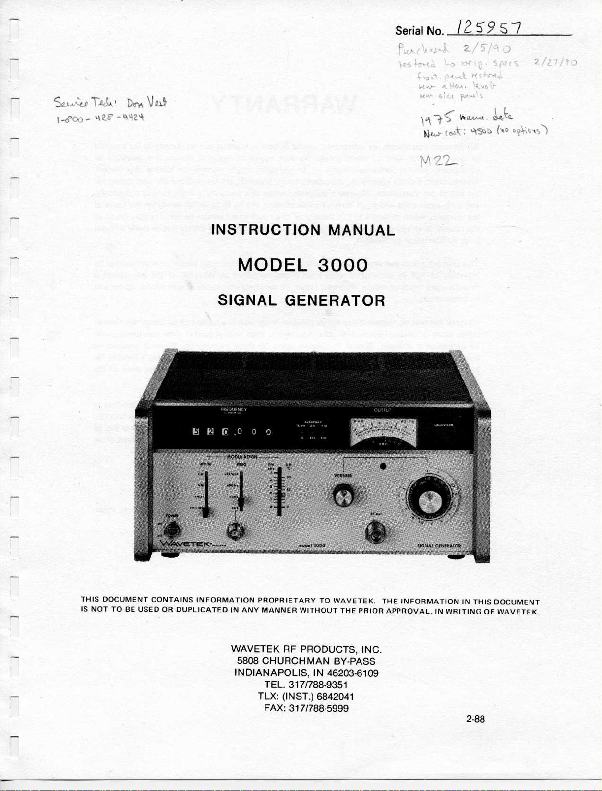
Serial
No
.
/2_5
1
q
s
THIS
IS
DOCUMENT
NOT
TOBEUSED
CONTAINSINFORMATION
OR
DUPLICATED
IN
WAVETEK
PROPRIETARY
ANY
MANNER
RF
5808
CHURCHMAN
INDIANAPOLIS,
TEL.317/788-9351
TLX:(INST.)6842041
FAX:317/788-5999
TO
WAVETEK
WITHOUT
PRODUCTS,
BY-PASS
IN
46203-6109
THE
PRIOR
INC
.
THE
APPROVAL,
.
INFORMATION
IN
IN
THIS
WRITINGOF
2-88
DOCUMENT
WAVETEK
.
Page 3
WARRANTY
All
Wavetek
of
one
component
Transfermatic
the
life
any
such
the
warranty
the
factoryorservice
prior
This
warranty
Wavetek,
defective
be
billed at
Wavetek
either
be
dangerousifmisused.Special
liability
breachofwarranty
specific
Any
be
reliable,
of
all
represent or
than
instruments
after
year
(except
Switch
of the
instrument.Wavetek's
instrument
when
authorization
does
or
not
in
as a
result
cost
.
assumes
aloneorin
for
instrumentshipped
recommendations
other
set
forth herein
no
conjunctionwith
secondary
but
Wavetek
warranties,
assume
date of
batteries)
assemblies,
which,inWavetek's
returnedtothe
centeristo
Wavetek
by
not
accordance
of misuse,
responsibility
chargesorconsequential
under
made
for
.
are
warranteed
manufacture.Wavetek
found
to
manufactured
obligation
factory or
prepaidbypurchaser.Shipment
be
.
applytoany
any
and
by
makes
expressed
Wavetek
products
with
instructions
improper
for
its
other
disclaimers
contractorotherwise
against
whichaclaimismade
Wavetek
no
warranty
or implied,
any
liability
against
defectsinmaterial
agreestorepairorreplace
defective
be
Wavetek,
by
under
this
opinion,
sole
to an
authorized
repairedoraltered
furnished
repair,orabnormal
product
equipment.High
for
of
apply
use
the
in
being
to these
damages
shall
of
its
resultstobe
and
no
connection
workmanship
and
under
normal
are
warrantyislimited
provestobe
service
by
conditions
usedina
voltage
instruments.Wavetek
any
and,
in
exceed the
not
.
products
obtained.This
representativeorpersonisauthorized
with
use
during
unconditionally
defective
center.Transportation
shouldnotbemade
persons
by
Wavetek.If
operations,
or
hazardousordangerous
usedinsome
event,
Wavetek's
purchase
are
based
upon
the
saleofour
foraperiod
any
assembly
this
period
warranteed
solelytorepairing
within
the
scope
without
not
authorized
instrument
the
repairs
manner
instruments
assumes
liability
price
tests
believed to
warrantyisin
products
or
.
for
of
to
by
is
will
may
no
for
of the
lieu
to
other
This
manual
tenance,
and
provides
repair
descriptive
of the
WAVE-IEKModel
SCOPE
material
OF
and
THIS
3000
MANUAL
instructions
Generator
Signal
for the
installation,
operation,
main-
Page 4
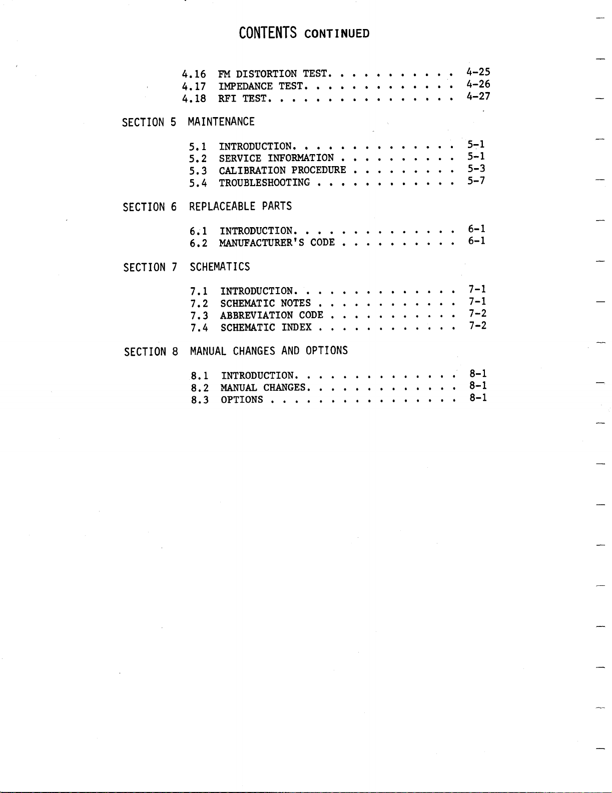
CONTENTS
SECTION
SECTION
SECTION
1
2
3
THEORY
3.3
3.4
3.5
3
3
3
3
3
.10
3
.11
3
.12
3
.13
3
.14
3
.15
GENERAL
1
.1
1
.2
1
.3
1
.4
OPERATION
2
.1
2
.2
2
.3
2
.4
2.5
2
.6
2.7
3
.1
3
.2
.6
.7
.8
.9
INFORMATION
INTRODUCTION
SPECIFICATIONS
OPTIONS
ACCESSORIES
INTRODUCTION
MECHANICAL
ELECTRICAL
DESCRIPTION
DESCRIPTION
INSTALLATION
OPERATING
OF
INTRODUCTION
OVERALLBLOCKDIAGRAM
C315
C316
DPS2A
DELETED
M9W
M10W
M172
M29-1
M30
M31
M32 - MHz
M33
M34
.
OPERATION
- METERBOARD
-
MODULATION
-
POWER
-
SWEEP
-
OUTPUT
-
SWEEP
FM
-
CRYSTAL
-
kHz
-
NARROW
-
WIDE
. . . . .
. . . . ...
. . . . .
.
. . . .
. . . . . .
INSTALLATION
INSTALLATION
OF
FRONTPANEL
OF
REARPANEL
CHECKS
PROCEDURE
.
. . . . . . . .
BOARD
SUPPLY
OSCILLATOR
AMPLIFIER
DRIVE/DAC
REFERENCE
SOURCE
STEPS.. . . . . . . . . . .
STEPS..
OSCILLATOR
OSCILLATOR
. . . .
. . . . .
. . . . . .
. . .
. .
. .
. . . .
. . . . . . . .
. . .
.
... .
. . . . . . . .
. . . . . . . . . .
. . . . . . ..2-7
. . . . .
. . . . . . . .
. . . . . . .
. ...
.
. . .
. .
. . . . .
. . . . . . .
LOCK
LOCK
. . .
. . .
.
. . .
. .
. . . . .
.
. . . . .
. . .
. .
. . .
. . .
. . . . . .
. . .
. . .
. .
. .
. .
. . . . . .
. . .
. . . . .
. . . .
. . . .
. . . . . .
. .
. .
.
.
. .
..2-4
. .
. . .
. .
..3-8
. .
. .
.
.
.
.
.
.
.
.
.
.
.
.
1-1
1-2
1-4
1-4
2-1
2-1
2-2
2-2
2-5
3-1
3-1
3-9
3-10
3-10
3-11
3-12
3-13
3-14
3-15
3-16
3-17
3-19
3-20
SECTION
4
PERFORMANCE
4.1
4.2
4
.3
4
.4
4
.5
4.6
4
.7
4
.8
4
.9
4
.10
4
.11
4
.12
4
.13
4
.14
4
.15
TESTS
INTRODUCTION
FREQUENCY
FREQUENCY
FREQUENCY
OUTPUT
HARMONICS
NON-HARMONIC
RESIDUAL
RESIDUAL
INTERNAL
PERCENTAM
AM
AM
FM
FM BANDWIDTH
LEVEL
AM
MODULATION
BANDWIDTHTEST
DISTORTION
DEVIATION
. . . . . . . . . . .
RANGE
ACCURACYTEST
STABILITY
TEST
FM TEST
ACCURACYTEST
AND
RESOLUTIONTEST
. . . . . . . .
TEST
ACCURACY
. . . . . . ... . . .
TEST
TEST
TEST
ACCURACY
TEST
TESTS
. . . . . . . . . . .
. . . . . . . . .
. . . . . . . . . . .
FREQUENCYTEST
. .
. . .
.
. . .
TEST
. . . . .
. . .
. . .
. . . . . . .
. . . . . .
.
. . .
. . . . . . .
. . . .
. . . . . . .
. . .
. . . . .
. . .
. . . .
4-1
4-2
.
4-3
.
4-5
.
4-5
.
4-11
.
4-12
.
.
4-14
.
4-15
4-16
.
4-17
4-19
4-21
4-22
.
.
4-23
Page 5
CONTENTS
4
.16
4
.17
4
.18
DISTORTION
FM
IMPEDANCE
RFI
TEST.. . . . . . ... . .
TEST
CONTINUED
TEST
. . . . . . . . . .
. . . . .
.
. . . . ...
. . " "
.
4-25
4-26
4-27
SECTION
SECTION
SECTION
SECTION
5
MAINTENANCE
5.1
5
.2
5
.3
5
.4
REPLACEABLE
6
6.1
6
.2
SCHEMATICS
7
7
.1
7
.2
7.3
7.4
8
MANUAL
8
.1
8
.2
8.3
INTRODUCTION
SERVICE
CALIBRATION
TROUBLESHOOTING
INTRODUCTION
MANUFACTURER'S
INTRODUCTION
SCHEMATICNOTES
ABBREVIATION
SCHEMATIC
CHANGES
INTRODUCTION
MANUAL
OPTIONS
...
INFORMATION
PROCEDURE
PARTS
INDEX
AND
CHANGES
. .
. . . .
. . . . . . . . . .
.
. . .
. . . . . . . . . . . .
CODE
.
. . . .
CODE
OPTIONS
.
. . . . . .
. . . . . .
. . . . . .
. . . . . .
. .
. . .
. . . .
. . .
. . .
. . . . . . . . .
.
. . . .
. . .
. . . . . .
. . . . . . .
. . . . . . .
. . . .
. .
. . .
.
. .
. . " " .
. . . . .
. . . . .
. .
. .
. .
. .
. .
. . "
5-1
.
5-1
5-3
.
5-7
6-1
6-1
7-1
"
.
7-1
7-2
7-2
8-1
8-1
8-1
Page 6
INTRODUCTION
1
.1
The
Model
solid-state
the
frequency
The
output
modulated
tween
1
The
front
which
addition,
mability
the
suited
test
The
on a
serves
the
frequencies
arefed
the
signals
its
In
overall
including
drift,
to
changes
is
kHz
to
1.1.2
+13
.1.1
FrequencyCharacteristics
frequency
panel
yield
Mode1
for
applications
accuracy
crystal-controlled
as
derivation
to
Model
specified
the
CW
incidental
line
.
accurate
peak
kHz
500
ModulationFeatures
3000
and the
and
is
.3000
a
phaselockedloops
3000
to an
and
accuracy
voltage
In
deviation
isarugged,
Signal
can
be
-137dBm
lever/indicator
a
resolution
remote
standard
both
of
stable
.
Thesereference
to
1
AM
short
the
to0.0017
peak
Generator
range
amplitude
level
of
the
frequency program
.Thisfeaturemakes
Signal
semi
.
the
instrument
frequency
of
various
provide
accuracy
MHz
modes
of
term
FM
changes
FM
mode,
and0.0017
deviation
of
and
to
the
and
completely
covering
1
to
520
or
frequency
canbe
.
unit
Generator
drift,
is
set
switches
of
1
kHz
fullyautomatic
is
oscillator
source
reference
frequencies
that
high
of0.0017
520
of
unit
variations
and
t10
stability
MHz
operation
is0.0017
long term
temperature
the
frequency
kHzup
t45 kHz
.
MHz
set
be-
via
.
ideally
based
that
for
enable
over
range
the
due
to
GENERAL
modulation
modulation
.
6
In
.
5
up
kHz
operation,
kHz
litude
With
of
FREQUENCY
tion,
tentiometer
vary
5
With
AM
switch
put
same
provides
variation
specific
ationcan
greater
over
1
The
frontpanel meter
dBmandVrms
dB
with
the
-137
Model
dB across
of
available
are
are
attainable
modulation
the
MODULATIONMODE
the
FM
the
the
output
kHz
or
500
the
MODULATION
positionand
in
amplitude
front
point
also
than
portions
.1 .3
OutputLevel
output
step
attenuator
an
11
userwith
.
dBm
3000
the
instrument
SECTION
INFORMATION
capabilities
frequencies
.In
peakdeviations
.In
to
positions
switch
frontpanel slide
can
kHz
the
panel
a reference
of
power
.
dB
The
is
the
in
be
frequency
range
the
vernier
can
slide
a
signal
of
interest
enable
20
milliwatts
of
the
A
fifteen-position,
vernier
a
range
calibrated
leveled
complete
.
of
the
the
907
switch
and
the
used
MODULATION
to
.
MODEswitchin
position
varied via
be
control
attenuator
levelaround
the
band
Features
is
indicated
calibrated
used
control
of
to
frequencyrange
.
Internal
400
Hz
FM mode
up to
AM mode
attainable
is
-
in
the
MODULATION
vernier
control
continuously
over
user
.
in
either
FREQUENCY
the
.
.
This
to
of
in
conjunction
provides
+13 dBm
output
within
1
and
500
amp-
either
posi-
po-
the
out-
the
This
for
oper-
obtain
power
on
both
of
the
±0
.75
1
of
.
a
a
a
10
to
The
nal
Model
and
3000also
external
featuresboth
amplitude
and
inter-
frequency
Page 7
GENERAL
1
.2
SPECIFICATIONS
1
.2.1
RANGE
READOUT
RESOLUTION
ACCURACY
STABILITY
1.2.2
INFORMATION
Frequency
RF
OutputLevel
1
MHz
to
520
6
digit
1
kHz
CW andAM modes
FMx1
FMx100
CW
and
FMx1
lever/indicator
(Typ
3
months
mode
mode
AM modes
mode
MHz
selectable
±0.0002%
<0
500
switches
±0
.001%
after
of
calibration)
±(0
.001%
±(0
.001%
.2
ppm/hr
Hz/10min
in1kHz
after
2
hours
+10
+45
.
.
15
kHz)
kHz)
steps
min
within
.
.
POWER
LEVEL
TOTALLEVEL
ACCURACYBREAKDOWN
1
.2 .3
IMPEDANCE
SWR
LEVEL
CONTROL
Output
RANGE
ACCURACY
Characteristics
+13
dBm
to
Continuously
with
dicated
+13
Flatness
Output
Step
50 ohms
<1
in
-7
<-77
.2
an
volts
to
-7
to
-77
dBm
Meter
Attenuator
RF
at
on
(±0
dBm
-137
adjustable
11
dB
vernier
a
frontpanelmeter
and dBm
dBm
dBm
(+13
.2
(±0
outputlevels
.
:
:
to -7 dBm)
:
:±0
dB
dB
.5
±1 .25
±1 .95
±2 .75
calibration
±1
calibration
(1
V
to .03
in 10
.
Outputlevel
dB
dB
dB
:
(Typ
.5
dB
.0
dB
to
below
±0
±0
±0
to
dB
(Typ
(Typ
(Typ
.75
.5
.5
70
error)
130
error)
0
vV)
steps
is
calibrated
±0
.75
±1 .25
±1
.5
dB
dB)
dB
dB
dB
V
.1
and
in-
dB)
dB)
dB)
1
.2 .4
HARMONIC
SUB-HARMONICS
Spectral
Purity
OUTPUT
>30dB
>26
Nonedetectable
below
dB below
fundamental
fundamental
from
from
10
520
10
MHz
MHz
to
1
to
Page 8
NON-HARMONICS
RESIDUAL
RESIDUAL
1
.2.5
FREQUENCY
AM
Amplitude
Internal
External
FM
Modulation
Fundamental
(MHz)
3
1
to
250
3
to
3
>65
post-detection
<200
bandwidth
3
NOTE
carrier
+3 dBm
+13 dBm
400
DC
required
vide
350
to
520
3
to
dB
below
Hz in 50
.
post-detectionbandwidth
kHz
:
These
level
if
.
Hz
and
20
to
kHz,
=10volts
calibrated
GENERAL
Non-HarmonicNon-Harmonic
1
to
3
to
3
to
3
to 1000
carrier
bandwidth
Hz
(Typ
100
specifications
<+3
thepeak
1
kHz ±5%
(3
(MHz)
3
250
350
to
15
Hz)
dBm
.AM
output
dB
bandwidth),
p-p
%
modulation
level
low
in a 50
.
kHz
Hz
<100
is
does
into
Hz
post-detection
possible
600
control
INFORMATION
be-
(dB
fundamental)
>60
>65
>55
>35
to
15
kHz
300
Hz
50
for
above
.
to
Hz)
a
level
pro-
in
.
(Typ
apply
not exceed
input
ohmto
RANGE
DISTORTION
MODULATIONCONTROL
ACCURACY
1
.2.6
Frequency
FREQUENCY
Internal
External
DEVIATIONPEAK
DEVIATIONCONTROL
ACCURACY
DISTORTION
Modulation
0 to
a
Calibratedfrom
DC to 25
required=
vide
kHz
90%
distortion
<3%
frequency
t(5%of
400
Two bands,
Calibrated
±250
±35
<4%
reading
Hz
and
calibrated
Hz
kHz
(3
to
deviation)
of
1
kHz,
10
0
from
on
xl
on x100
10
to70%
1
+5I) atafrequency
kHz,
(1
volts
to5kHz,
range
kHz
at
AM(:<5%
kHz
(Typ
<1 .5I to
0 to
deviation
1001
±5%
dB
bandwidth),input
into
p-p
control
and
0
to
5
kHz, xl
range
deviation),
a
frequency
600
0
to
ohms
to
and
<2%
of
AM)
90%
30%
of
to
.
500 kHz
x100
(10
to
1
kHz
AM)
1
level
at
kHz
pro-
500
Page 9
GENERAL
1
.2.7
1
.2.8
OPERATING
OUTPUT
RFI
POWER
DIMENSIONS
INFORMATION
Programmability
General
TEMPERATURE
CONNECTOR
Frequency
input
or
BCD-coded
25 t5
oC,
25
t15
fications
Type
N
<1
VV
diameter
fromanysurface
ceiver
115/230
12
in
high,
is
connectorusing
contactclosures
all
specifications
0C,
with
is
induced
loop
;
V
±10%,
.
(30.3cm)
13
3/4
in.(34.9am)
programmablevia
BCD-coded
slight
which
.Loop
50/60
in
is
wide,
a
degradation
two-turn,
held
feeds
40
Hz,
5k in
long
TTL
.
apply
one
a
VA
.
rear
panel
voltages
of
speci-
one-inch
inch away
ohm
50
(13
re-
.4
cm)
WEIGHT
1
.3OPTIONS
1.3:1
RF
Level
Programming
25 lb
shipping
Options
Option
For
are
a standard
in
output
Option
dB in
rear-panel
dBm
Continuously
-97 dBm
VERNIER
providedby
Option
plug)
Front-panel
Reverse
by
.
1A, 1B, 4,
3
bothOptions
calibrated
Programmable
is
lA
.
.
1B
in 10
attenuators
is
dB
.
also
this
(11.4kg)
.
may
0
provided
power
option
net,
and7are
be
factory
1A
and
for
+13 dBm at
unit,
onlyguaranteed
Program
.1
plug)
Front-panel
in 10
Reverse
Program
steps
dB
.
but
Attenuators,
Level
dB
adjustable
this
reference
Level
steps
.
0
dB
power
option
Level
(programmed
Remotecontrol
.
Range
protection
.
30 lb.(13
factoryinstalled
or
field
1B,
the
to
due
dB
steps
:See
greater
to
+12
Range
(programmed
reference
level
from+13
and
protection
.
Range
via
set
by
of
Section1.2.2
is
also
:
:
.6
installed
instruments
50
MHz
losses
a
calibrated
dBm
.
0
to
is
range
dBm
an
11
is
0
to 90 dB
rear-panel
front-panel
CW/AMmode
provided
like
109
also
kg)
.
.
.9
via
+13
:
to
dB
.
Page 10
1
.3 .2Reverse
1
.3.3
1
.3.4
1
.4
Furnishedwithinstrument
Additional
Auxiliary
Low
ACCESSORIES
PowerProtection
RF
Output
Leakage
Accessories
Option
if
DC
are
accidentally
connector
whenusingoption
Option"4"
signal
nector.Normally
counter
Option
of
Section
Instruction
Rear-panel
Rack
Mount
Programmers
control
levels,
Module
preventsdamage
"3"
V
(100
available
.
7
Service
max)
.
(This
provides
reduces
1
.2.2
Manual
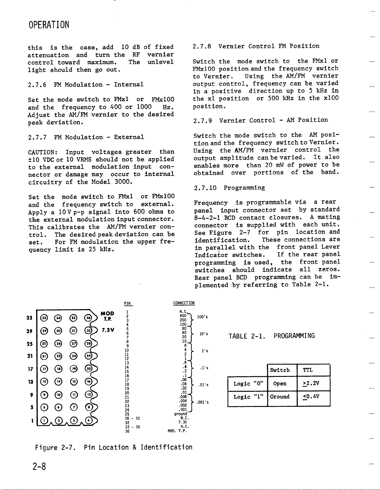
PROGRAMMING
Kit,
for
of
selectedfrequencies
Series
GENERAL
or RF
applied
option
lA
or
a
fromarear
used
K108
single
3900
Kit,
to
the
leakagespecification
by a factor
.
K004
INFORMATION
the
to
W
to
is
.
panel
drive
and
max)voltages
the
not
of
(50
1B)
leveled
plug
push-button
instrument
RF
output
required
(-10
BNC
frequency
a
10
.
pins
or GPIB
and
output
dBm)
con-
Page 11
2
.1
INTRODUCTION
This
lation
Wavetek
The
installation,
front
lationchecks
2.2
2.2
sectionprovides
and
operating
Model
instructions
and
rear
MECHANICAL
.1
Initial
complete
instructions
3000
electrical
panel
and
Inspection
signal
consist
operatingprocedures
INSTALLATION
of
installation,
features,
instal-
for the
generator
mechanical
instal-
SECTION
2
OPERATION
and
Retain
material
The
.
.
will
replacement
without
ments
2
.2 .3
the
local
immediately
.
ZackMounting
Item
shipping
for the
representative,
or
repair
waiting
for
CONTENTS
Qty
carton
carrier's
arrange
of
damage
(K108)
or
for
your
claim
packing
inspection
the
factory
either the
instrument,
settle-
PartNo
.
.
After
inspect
to knobs,
The
erialshould
necessary
2.2 .2
If
damaged
and
representative
unpacking
the
connectors,
shippingcontainer
to
DamageClaims
the
instrument
in
either
the
external
be
reship
transit,
the
or
instrument,
parts
surface
and
saved
is
receivedmechanically
nearest
the
the
notify
factory
in
unit
visually
for
areas,
packing
case
.
the
Wavetek
in
damage
etc
mat-
it is
carrier
area
Indiana
A
(Insert)
B
(Side)
.
.
C
(Screw)
D
(Screw)
Procedure
Remove
Mount
panel
the
screws
longer
eration
:
the
items
of
the
than
for the
2
ea
2
ea
8
ea
4
ea
(See
Figure
screws
A
and
instrument
provided
screwsC.)Repeat
other
from
B
.
2-1)
one
against
and
(Screws
side
B001-145
0001-146
HS101-808
HS101-810
side
secure
of
the
the
the
panel
side
with
D
unit
.
are
op-
.
Figure
2-1.
K108 Rack
Mount
Page 12
OPERATION
2
.3
ELECTRICAL
The
instrument
volt
AC
selected
the
rear
instrument,
in
the
Rear
ponds
to
or
by a
panel
the
INSTALLATION
operates
230
volt
SlideSwitch
.
Before
check
Panel
that
Fuse Holder
correct
from
AC
supplymains
the
value
FREQUENCY
I-SYO
MH
either
located
operating
fuse
for
-
mounted
corresthe
O
~
115
as
on
the
se-
1007
ACCURACY
3700td0
-KHZ
lected
volt
The
voltage,
AC
power
operate
mains
.
Instruments
for
operation
less
specified
operation
.
5
KH
RMS VOLTS
and
from
.
0
supply
are
OU
dBm
i.e
.5
either
shipped
at
115
for
PUT
.,1.0
amp for
has
been
50 or 60
volt
230
7
9
from
volt
amp
for
230
volt
designed
Hz
the
AC
60
AC
UNlE0LE0
a
115
AC
to
supply
factory
Hz
un-
or 50 Hz
a
.
MODULATION
FREO
VERNIER
400Hz
1KHz
EXT
-
POWER
off
~~
WAvET
MODE
CW
AM
FMxI
FM
x100
V
iE
Figure
2
.4
DESCRIPTION
OF
FRONT
PANEL
AM
FM
4
3
z
I
0 0
90
50
model3000
2-2
VERNIER
\
a
RF
out
.
Front
Panel
'fff
SIGNAL
GENERATOR
0
2-2
Lever
Indicator
Switches
Select
from
and
indicatedesired
1
to
520 MHz
witha1kHz
output
frequency
resolution
.
Page 13
OPERATION
O2
AccuracyLamps
O3
Output
4O
Unlevel
LevelMeter
Lamp
Indicate
and
AM
modes, ±(0
±(0
.001%
lamp
willflash
is
turned
steady
phase-locked
dication
light
lock
identified
looking
light
Indicates
in
VRMS
Indicates
not
light
indicates
loops
for the
.)
and
validwhen
frequency
.001%
+
45 kHz)
for
on
.Under
indicates
and the
is
valid
is
by
outputlevel
dBm
that
.
that
open
removing
corresponding
.
the
the
accuracy
in
FMx100
a
few
frequency
A continuouslyflashing
one
.(The
outputlevel
lamp is on
.±0
+
10
.Typically
seconds
normal
that
or
more
open
the top
over
.001%
kHz) in
after
operationa
the
accuracy
of
loop
cover
"module
a
10 dB
accuracy
.
FMxl
unit
thephase
in
CW
and
the
power
is
in-
canbe
and
fault"
range
is
O5
Attenuator
6O
Vernier
O7
AM/FMVernier
FrequencySwitch
Controls
from+10to
is
calibrated
Controls
range
Is
calibrated
tion
mits precise
mode
tively
1
kHz
manualamplitude
the
frequency
provides
the
modeswitch
vides
quency
FMxl
Selects
frequencyicontrol,
modulation
.
and
switch
and the
or
up
change
and
the
outputlevel
theoutputlevelover
from
in
Ext
.
up
toa+5
FMx100
vernier,
and
-130
dBm
in
dB
from
O to
0
to
90%
AM
and
AM
and
frequency
Thevernier
and
switch
to
+6 dB
is
in
kHz
when
respectively
for
400Hz
external
over
a140
.TheAttenuator
and
VRMS
.
kHz
FM
5
AM
.This
FM
FMxlor
frequency
vernier
in
amplitude
the
or up
mode
the
manual
modulation
settings
switch
also
AM
to
and1kHz
peak
control
FMx100
serves
control
.Thevernier
change
and
+500
switch
.
amplitude
dB
range
dial
an
11
devia
per-
with
respec-
in
400
as
with
when
also pro-
kHz
fre-
is
internal
.
dB
the
Hz,
a
in
or
O9
Ext
Modulation
nal for
V peak-to-peak
dance
A
lesser.input
portional
FMvernier
peak
AM
calibrates
full
.
signal
input
and
acceptsaDC to 20
a
DC
signal
the
voltagewill
scale
Therefore,
into
600
to
25
into
AM/FM
vernier
calibration
a1volt
ohms
kHz for
a
600 ohm
result
will
kHz
FM
full
in
of
peak-to-
result
sig-
.
A
impe
scale
a pro-
the
in
2-3
10
.
AM/
a
Page 14
OPERATION
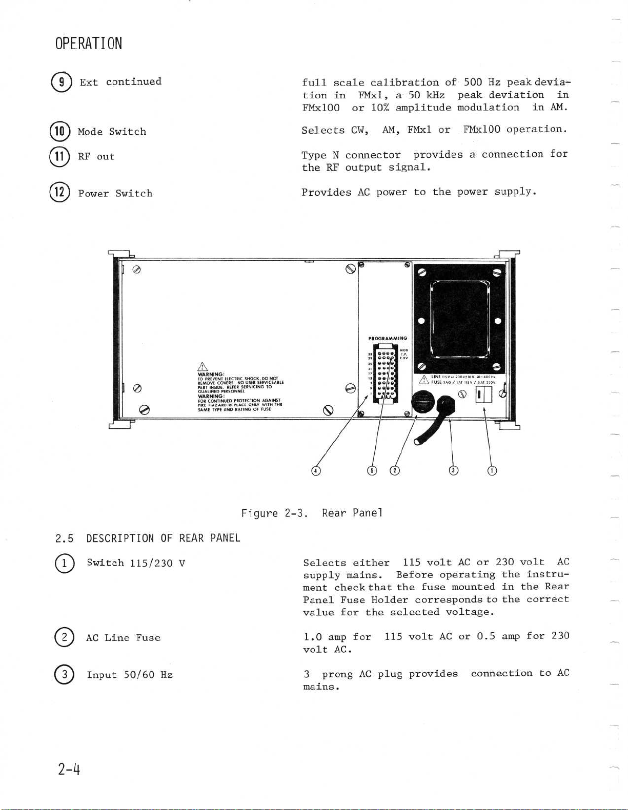
(D
continued
Ext
ModeSwitch
RF
out
Power
Switch
WARNING
TO
PREVENT
REMOVE
PART
QUALIFIED
WARNING
FOR
FIRE
SAME
ELECTRIC
COVERS.NO
INSIDE.REFER
PERSONNEL
:
CONTINUED
HAZARD
TYPE
AND
SHOCK,DONOT
USER
SERVICING
PROTECTION
ONLYWITH
REPLACE
RATINGOFFUSE
SERVICEABLE
TO
AGAINST
THE
full
tion
FMx100
Selects
Type
the
RF
Provides
scale
in
or
CW, AM,
connector
N
output
calibration
FMxl,
10%
AC
power
a
50
amplitude
FMxl
provides
signal
to
kHz
.
of
or
the
Hz
500
peak
deviation
modulation
FMx100
a
connection
power
peak
operation
supply
devia-
in
.
AM
for
in
.
.
2
O
.5
DESCRIPTION
Switch
AC
Input
Line
115/230
Fuse
50/60
OF
Hz
REAR
V
PANEL
Figure
2-3
Rear
.
Selectseither
supply
ment
Panel
value
1 .0
amp
volt
3
prong
mains
Panel
115
mains
checkthat
FuseHolder
fortheselected
AC
.
.
for
AC
.
115
plug
Before
the
volt
operating
fuse
mounted
correspondsto
voltage
volt
AC or0.5
provides
AC
or
connection
230
volt
the
instru-
in
the
the
correct
.
ampfor230
to
AC
Rear
AC
Page 15
OPFRATION
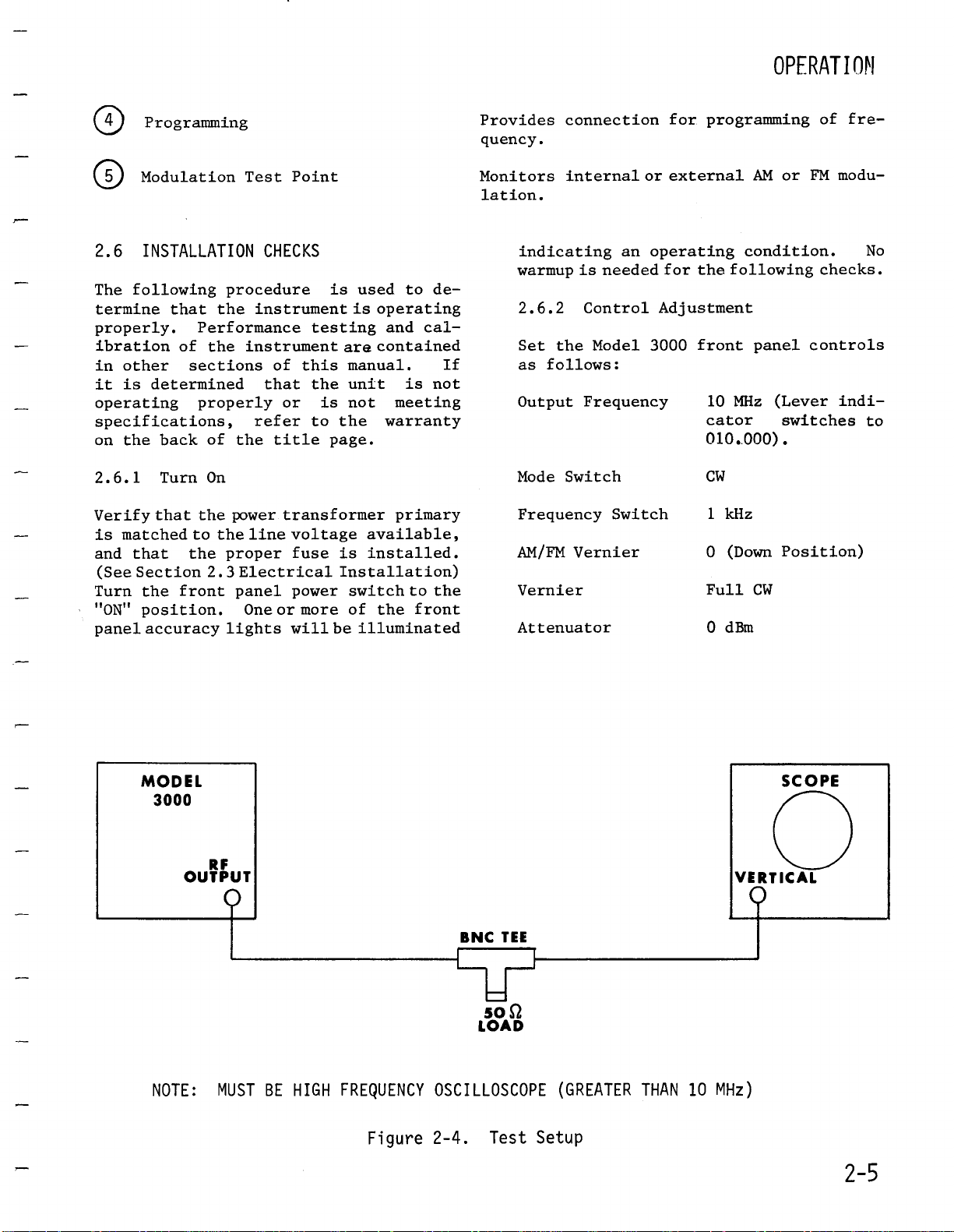
Programming
O5
Modulation
2.6
INSTALLATION
The
following
termine
properly
ibration
in
other
it is
operating
specifications,refer
on
2.6.1
Verify
is
matched
and
(See
Turn
"ON"
panel
that
.
of
sections
determined
the
back
TurnOn
that
to
that
Section2.3
position
the
front
accuracy
the
Performance
properly
procedure
the
the
of
the
the
proper
.
lights
Test
CHECKS
instrument
instrument
of
that
title
the
power
line
Electrical
panel
One
Point
is
testing
this
the
or is
the
to
page
transformer
voltage
fuse
is
Installation)
power
or
more
willbe
used
operating
is
and
contained
are
manual
unit
meeting
not
warranty
.
primary
available,
installed
switch
of
the
illuminated
to
.
is
to
front
de-
cal-
not
the
Providesconnection
quency
Monitors
lation
If
.
.
.
indicating
warmup
2.6 .2
Set the
as
follows
Output
ModeSwitch
Frequency
AM/FM
Vernier
Attenuator
for
internal
is
ControlAdjustment
Model
Frequency
Vernier
an
needed
:
Switch
or
external
operating
for
3000
programming
AM
condition
following
the
frontpanel
10
MHz
(Lever
cator
010..000)
CW
1
kHz
0
(Down
Full
CW
0
dBm
of
or
FM modu-
.No
checks
controls
switches
.
Position)
fre-
.
indi
to
NOTE
SCOPE
VERTICAL
BNC
TEE
SO
SZ
LOAD
MUST
:
BE
HIGH
FREQUENCY
Figure 2-4
OSCILLOSCOPE
.
Test
(GREATERTHAN
Setup
10
MHz)
2-5
Page 16
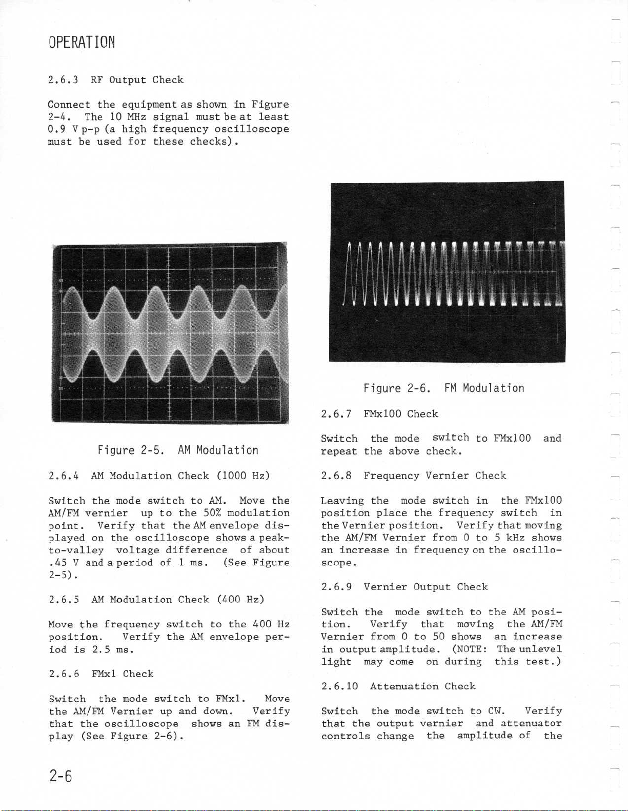
OPERATION
2
.6 .3
RF
Output
Check
Connect
2-4
.
0.9V
must
p-p
be
The
the
(a
used
equipment
10
MHz signal
high
for
as
frequency
these
checks)
shown
must
beat
oscilloscope
in
.
Figure
least
Figure 2-6
.
FM
Modulation
Figure
2.6 .4
Switch
AM/FMvernier
point
played
to-valley
.45
2-5)
2
.6.5
Move
position
iod
2
.6.6
Switch
the
that
play
AM
Modulation
the
Verify
.
on
the
V
andaperiod
.
AM Modulation
the
frequency
.
is
2.5ms
FMxl
the
AM/FMVernierup
oscilloscope
the
(See
Figure
2-5
mode
voltage
switch
up to
that
oscilloscope
Verify
.
Check
mode
AM
.
Check
the 50%
the
difference
of1ms
Check
switch
the
switch
and
2-6)
.
Modulation
(1000
to
AM
AM
envelope
showsa
.(See
(400
to
AM
envelopeper- Vernier
to
FMxl
down
shows
Hz)
.
Move
modulation
peak-
of
about
Figure
Hz)
the
400
.Move
.Verify
FM dis-
an
the
dis-
Hz
2
.6 .7
Switch
repeat
2
.6 .8
Leaving
positionplace
the
the
an
scope
2
.6
Switch
tion
in
light
2.6
Switch
that
controls
FMx100Check
the
mode
the
above
FrequencyVernierCheck
the
Vernier
AM/FMVernierfrom
increase
.
.9
.
output
.10
the
position
Vernier
the
mode
Verify
from
amplitude
may
come
AttenuationCheck
the
mode
output
change
mode
the
in
frequency
Output
0
to 50
switch
check
switch
frequency
.
switch
that
.
on
during
switch
vernier
the
to
FMx100
.
in
the
switch
Verify
0
Check
moving
shows
(NOTE:The
amplitude
that
to
5
on
the
to
theAM posi-
an
this test
to
CW
and
attenuator
and
FMx100
moving
kHz
shows
oscillo-
AM/FM
the
increase
unlevel
.Verify
of
the
in
.)
2-6
Page 17
OPFRATION
signal
The
2.7
No
beyond
stallation
2.6.
perform
the
warmup
2.7 .1
Verify
mary
available
installed
Installation
switch
accuracy
indicating
NOTE
lights
This
onds
refer
title
to be
specifications,
ately,
required
NOTE
transceivers,
to
applied
Damage
circuitry
pens
2
.7 .2
Select
six
front
520 MHz can
resolution
displayed
instrument
OPERATINGPROCEDURE
preparation
completion
To
insure
as
stated
instrument
before
TurnOn
that
is
matched
and
"ON"
lights
:A
.If
:Whenworking
keep
.
Lever
flashing
indicates
should
to
thewarranty
page
.If
used
otherwise
.
voltage
to
may
occur
of
Frequency
the
panel
.
on
the
is
now
for
operation
checks
the
(See
.Turn
.One
an
cease
the
to
the
etc
the
the
frequencydesired
Indicator switches
.
A frequency
be
that
in
should
using
power
to
that
Section
or
will be
operating
an
in
flashing
the
extreme
it
a
.,
or RF
RF
to
the
Model
Selection
selected
contained
withactive
ready foruse
of
the
the
Model
the
specifications,
have
.
transformer
the
the
proper
2
.3
the
more
indication
unlocked
a
matter
does
on
the
unit
can
be
two
hour warmup
care
output
should
power
output
3000
is
limits
between
with
oscilloscope
is
required
initial
in
Section
3000
a
two
line
front
usedimmedi-
voltage
fuse
Electrical
panel
frontpanel
illuminated
condition
on
condition
of
not
cease,
back
if this
of
not
going
of
circuits,
be used
from
being
connector
attenuator
hap-
with
on
1
a
1
in-
will
hour
pri-
the
sec-
the
its
the
the
and
kHz
is
is
2,7
.
.
.
.
.
.3
OutputLevel
Set
the
output
to
the
desired
continuously
-137
attenuator
equals
dBm
output
imum
ceeded
indicating
2.7 .4
Set
quency
modulation
nier
depth
2
CAUTION
±10
to
nector
circuitry
Set
quencyswitch
V
nal
calibrates
The
set
input
NOTE
taken
level
unlevelcondition
cases,
cause
the
This
PINdiode
causean
lation
.7
.5
the
p-p
modulation
desired
.The
RF
dBm
range
the
is
as
long
does
output
the
unlevel
AM
Modulation
the
mode
switch
to
indicate
.
AM Modulation
:
Input
VDC
or 10
external
or
damagemay
of
the
mode
signal
upper
is
20
:
When
not
to
or
excessive
a
high
the
unlevel
vernier
is
caused
leveler
increase
added
RF
possible
as
not
level
an unleveledcondition
switch
rate
the
switch
into
the'AM/FM
modulation
kHz
AM
exceed
Selection
attenuator
level
adjustable
.The
to
the
output
the
to
.
VRMS
to
.
modulating,
%
by
.NOTE
at
peak
exceed
.If
light
to
either
Adjust
the
desired
voltages
should
modulation
Model
to
external
600
input
frequency
the
distortion
can
of
AM modulationmay
light
control
the
which
in
and
.
The
output
over
level shown
meter
levels
of
the
this
will
-
Internal
AM
-
External
occur
3000
AM
ohms
connector
Vernier
depth
+13
exist
to
is
bottoming
distortion
indication
:
the
+13 dBmmax-
level
illuminate
and the
400
or 1000
the
AM/FMvermodulation
greater
not
be
input
to
.
and the
.
Apply
to
the
can
limit
care
dBm
.In
come
at
in
vernier
a
+13
on
AM
modu-
above
modulated
is
ex-
.
fre-
than
applied
con-
internal
frea 10
Exter
.
This
control
then
of
this
must
maximum
and
some
on
when
minimum
of
the
turn
can
.If
is
to
the
+3
Hz
.
be
be
an
.
2-7
Page 18
OPERATION
this
is
the
attenuationand
control
light
2.7.6
Set
and the
Adjust
peak
2.7 .7
CAUTION
t10 VDC
to
nector
circuitry
Set
and the
Apply
the
This
trol
set
quencylimit
toward
should
FM Modulation
the
modeswitch
frequency
the
deviation
FM
:
or
the
external
or
the
modeswitch
a 1OVp-p
external
calibrates
.The
.For
then
AM/FM
Modulation
Input
10
VRMS
damage
of
the
frequency
modulation
desired
FM modulation
is 25
case,
maximum
vernier
.
voltages
modulation
.may
Model
signal
the
10
dB of
RF
the
.
The
.
Internal
FMxl
or
or 1000 Hz
to
the
External
turn
go
to
add
out
-
to
400
greater
should
not
be applied
input
occur
to
switch
3000
FMxl
into
input
to
.
to
600
connector
or
external
AM/FMverniercon-
deviation
peak
the
upper
kHz
.
fixed
vernier
unlevel
FMx100
desired
than
con-
internal
FMx100
ohms
canbe
fre-
to
2.7 .8
Switch
FMx100
to
output
in
the
.
position
2.7 .9
Switch
tion
Using
output
enables
obtained
2.7
.
Frequency
panel
.
8-4-2-1
connector
See
identification
in
VernierControl
the
position
Vernier
.
control,
positive
a
xl
position
.
Vernier
the
mode
and
the
the
AM/FM
amplitudecan
more
over
Programming
.10
is
input
BCD
is
Figure
parallel
mode
switch
and the
Using
frequency
direction
or
Control
switch
frequency
than
portions
programmable
connector
contact
supplied
2-7 for
.
with
the
Indicatorswitches
programming
switches
panel
Rear
plemented
is
should
BCD
by
referring
used,
programming
FM
frequency
the
500 kHz
switch
vernier
be
20
mW
closures
pin
These
front
.If
indicate
Position
to
the
AM/FM
can
up to
in
-
AM
Position
to
the
to
control
varied
of
of
.
power
the
via
set
by
.
with
each
location
connections
panelLever
the
rear
the
frontpanel
all
canbe
Table
to
FMxl or
switch
vernier
be
varied
kHz
5
the
AM posiVernier
It
to
band
a
rear
standard
mating
A
unit
panel
zeros
2-1
in
x100
.
the
also
be
.
.
and
are
.
im-
.
33
29
25
21
17
13
9
5
Figure
2-8
2-7
PIN
MOD
T.P
7
.3V
.
Pin
Location
1
2
3
4
5
6
7
8
9
10
11
12
13
14
15
16
17
18
19
20
21
22
23
24
25
26 - 31
32
33-35
36
&
Identification
CONNECTION
N.C.
400
200
100
80
40
20
10
.08
.04
.02
.O1
.
oo8
.004
.002
.001
ground
N.C.
7.3V
N.C
MOD.T.P.
100's
10's
8
4
1's
2
1
.8
.4
.2
.1
.O1's
.001's
.
TABLE
Logic
Logic
2-1
"0"
"1"
.
PROGRAMMING
Switch
Open
Ground
TTL
>2
<0
.2V
.4V
Page 19
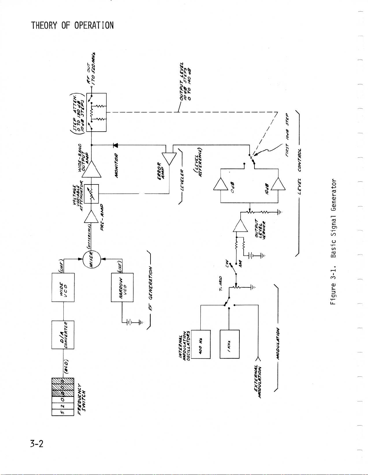
3.1
Section
analysis
brief
the
contain
each
For
subassemblies,
in
3.2
TheModel
controlledoscillator
locked
havebeen
resolution
Thediscussionwill
basic
scribehow
vide
3.2
This
RF
is
amplified,
lated
Refer
of
phase
RF
The
twoUHF
outputs
erodyned
INTRODUCTION
3.2presents
to
enable
overall
instrument
more
subassembly
actual
Section
OVERALL
loops
signal
the
additional
.1
Basic
discussionbriefly
is
generated
controlled,
.
to
Figure
the
basic
locking
GENERATION
RF
output
oscillators
of
in
view
.
detailed
wiring
7
of
BLOCK
3000
is
and
added
.
generator
the
Signal
also
leveledand
3-1'
signal
.
frequency
the two
the
mixer
.
refer
the
essentially
for the
phase-locked
and
a
block
the
reader
of
the
Sections
descriptions
of
the
to
the
manual
DIAGRAM
to
which
a
crystal reference
highfrequency
first
accuracy
Generator
how
how
for
and
oscillatorsare
dealwith
then
describes
its
the signal
amplitude
a
block
generator
is
a mixer
.Thedifference
to
operation
3
.3
chassis
schematics
.
a
it
will
loops
.
frequency
without
generatedby
diagram
get
-3.15
and
voltage
phase-
the
de-
pro-
how
the
modu-
diagram
.
The
het
of
of
is
a
THEORY
frequency
output
The
are
their
Oscillator
The WideOscillator
over
Narrow
Narrow
RF FREQUENCY
The
by programming
Wide
tor
front panelFREQUENCY
BCDoutput
verted
grams
This
mately
RF
The
stage,
output
leveling
lifier
The
Error
Attenuator
peak
This
reference
of
(voltage
changes
Amp
a
DC
amplifier
frequencies
controlled
varactor diodes
a
range
Oscillator
frequency
RF
output
Oscillator
is
ultimately
to
the
analog
3
AMPLIFICATION
RF
power
wide-band
is
.
Leveler
Amplifierand
of
detected
Error
the
the
until
level
OF
is
amplified
byDC voltages
yields
from
CONTROL
frequency
of
these
an
analog
oscillator
signal
MHz accuracy
is
maintained
system
includesaMonitor
.
The
the
output
level
by
the
Amp
variable)
inputlevel
the
monitored
equal
SECTION
OPERATION
and fed
.
of
these
.
a
single
can
the
frequency
to
520
.
the
frequency
.
TheWide Oscilla-
controlled
switches
switches
voltage
in1MHz
can
provideapproxi-
.
AND LEVELING
amplified
amplifier
by
around
Monitor
Error
to
this
a
VoltageVariable
of
the
is
compared
Amp
is
fed
attenuator,
signal
the
reference
oscillators
applied
The
frequency
be
programmed
MHz
is
determined
whichpro-
by
.
a
closed-loop
Output
detects
Output
.
The
to
a PIN
to
the
to
Narrow
of
above
of
by
.The
is
steps
a multiThe
Diode,
toaDC
output
diode
which
Output
produces
level
3
the
to
the
the
the
the
con-
flat
Amp-
an
the
Amp
.
.
.
.
Page 20
THEORY
OF
OPERATION
k
-
Q
0
30
0
`
~Q
o
Wo
a
vW
tih?
W
h
e
0
h
0
0
s
LVA
WQ
>m
Oc
W
W
V
a
0
.
~IHn
V
C'3
r
N
N
m
0
Q)
Q)
fCS
Qs
U
3-2
00
0
2
W
=h
2~ti
~Vv
O
0
0
i
N
to
h
n
20
ka
Page 21
LEVEL
The
circuitry
output
above
the
DC
output
Of
the
passive
dB is
reference
hasa10
is
provided
erence
vided
output
highest
Since
trolled,
plying
VERNIER
reference
CONTROL
level
leveling
level
level
150
dB
attenuation
controlled
.
dB
range
range
that
so
ampcan
possible
the
RF
AM
the
level
voltage
AND
AM
for
controlling
is
directly
system
reference
.
output
.
by
The
VERNIER
.
by
switchingthe
.This
when
AM
provide
power
level
can
be
modulating
control
to
related
because
changes
range,
The
remaining
changing
output
The
remaining
range
is
can
accomplished
switch
notrequired
a
carrier
.
be
voltage
signal
.
This
the
Error
the
changing
130
the
control
level
causes
to
the
dB
is
at
by
to
Amp
the
level
10
refpro-
the
the
con-
apthe
the
RF
RF
20
dB
is
to
change
ing
from
fromanexternal
3 .2 .2
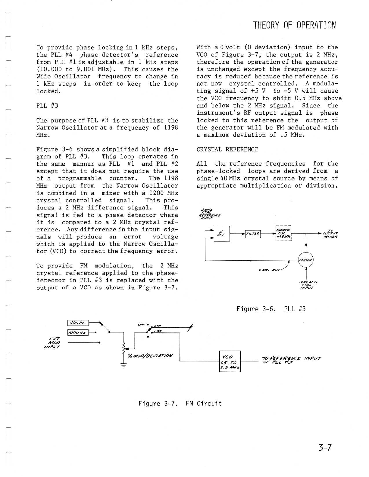
The
Section
1
leveled
lity
the
curacy
tion
solution
ment
Phase-locked
are
and
3-1
in
and
signal
basic
to
above
.
used
tune
.
PLL
allows
at
the
.
one
of
Phase-Locked
signal
3 .2 .1
MHz,
520
and
to
be
circuitry,
is
only
To
achieve
and
includes
to
it in
The
NarrowOscillator
#3
two
adjustable
amplitude
.001%
stabilize
which
FM
THEORY
frequency
The
modulating
internal
source
generatordiscussed
has
has
3
MHz
the
accuracy,the
four
loops
1
kHz
provides
operation
of
.
Loops
a
frequency
an
output
andhas
modulated
however,
with
desired
phase-locked
(PLL)
the
Wide
steps
.
OF
OPERATION
the
modulat-
signal
oscillators
range
which
the
.
the
1
MHz
resolu-
1
kHzre-
instru-
#1,
#2
and
Oscillator
.
See
is
included
stabilization
abi-
With
ac-
loops
Figure
is
or
in
of
is
.
#4
lIvAVr
AROrfRAM
.000
r
.999
/
KHz
X7-AL
REF
OUroar
I I
-
-
/0,000
.9,999
9,00/
OUTPUT
/0
.000
9
.999
9
.00/
4A/Z
Figure
3-2
.
PLL
#1
3-3
Page 22
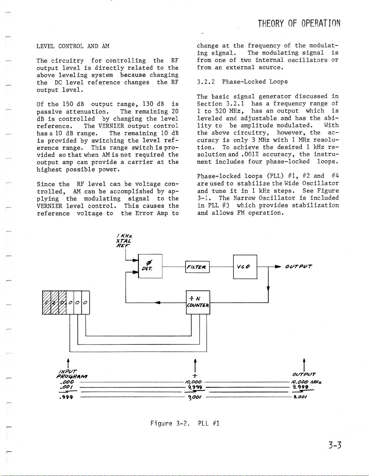
THEORY
PLL
The
CW
signal
from
panel
from
will
PLL
Figure
gram
#1
purpose
10
.000
frequency
.000
be
#4
.
3-2
of
OPERATION
OF
of
PLL
which
to
9
MHz
to
used
as
showsasimplified
PLL
#1.It
controlledoscillator
cies
from
9 to 10
the
.
it is
.
VCO
andajN
signal
mable
counter
panel
from
counter
from
counter
is
kHz
the
tectorwhere
controlled
selector
counter
#1
changes
.001
MHz
selector
.999
MHz
a
reference
consists
capable
MHz,
A
sample
is
The
by
switches
is
fed
compared
to
is
in
.
a
phase
fed
divisor
the
to a
generate
1
kHz
as
the
is
switched
This
signal
block
ofavoltage
of
frequen-
detector
of
the
to a
program-
of
three front
.The
phase
to
a
steps
front
signal
for
dia-
output
the
output
de-
1
kHz
crystal
a
input
not
is
the
phase
exactly
PLL
The
CW
from
panel
000.to
then
the
this
lator
tion
reference
signals
the
same
produced
to
frequency,
.This
frequency
detector
1
kHz
.
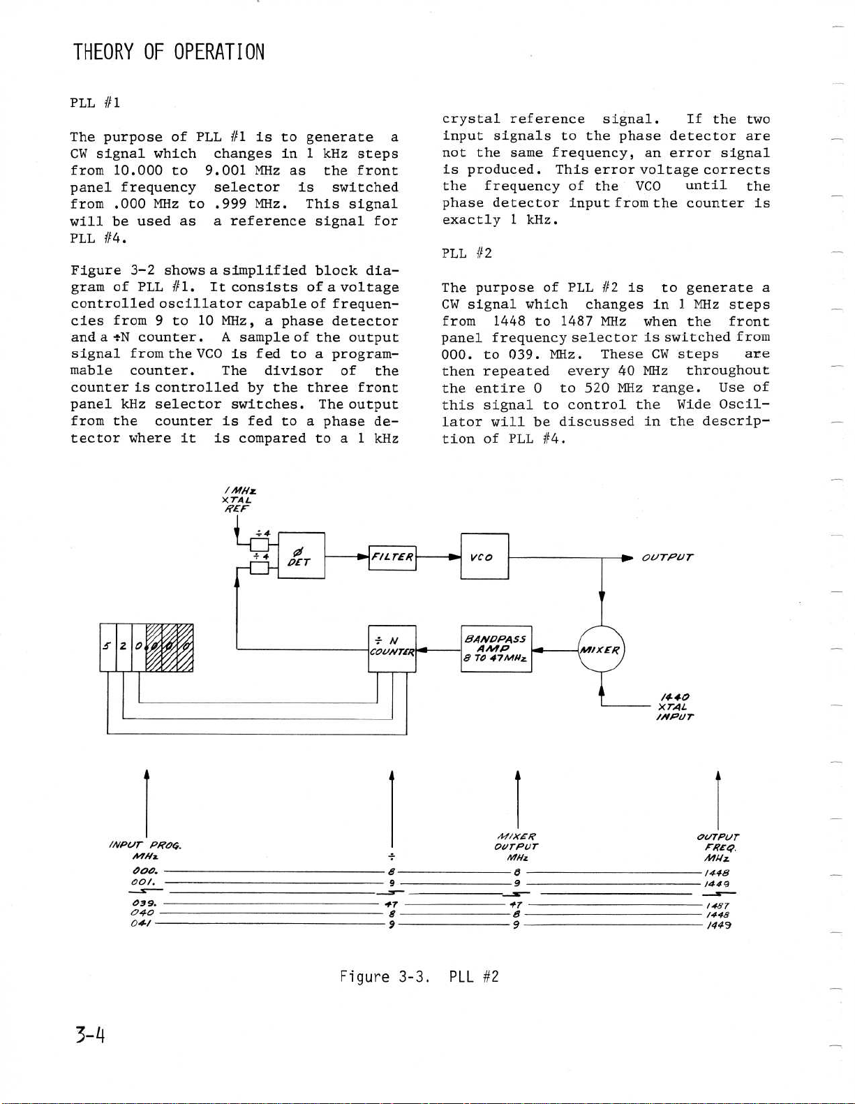
#2
purpose
signal
1448
of
which
to
1487
frequencyselector
039
.
MHz
repeated
entire
signal
willbe
of
PLL
0
to
to
discussed
#4
.
signal
the
error
of
the
input
PLL
#2
changes
MHz
.
These
every
520
control
phase
VCO
from
is to
40
MHz
the
.If
detector
an
error
voltage
the
in
when
is
switched
CW
MHz
range
in
the
the two
signal
corrects
until
counter
generate
1
MHz
the
steps
throughout
.
Use
Wide
Oscil-
descrip-
are
the
is
a
steps
front
from
are
of
/NP!/T
r
000
00/
039
040
04/
PROG-
.
.
.
l
XTAL
REF
MHz
-s-
MIXER
OUTPUT
MHz
-
9
_
47
9
9
8
-
9
s
-
47
B
9
OUTPUT
FREQ,
iYlNz
/448
/449
___Sr-
1487
/448
/449
3-4
Figure
3-3
.
PLL
#2
Page 23
Figure
gram
the
ception
and
this
the
VCO
necessary
compatible
and
circuits
as
programmable
the
the
PLL
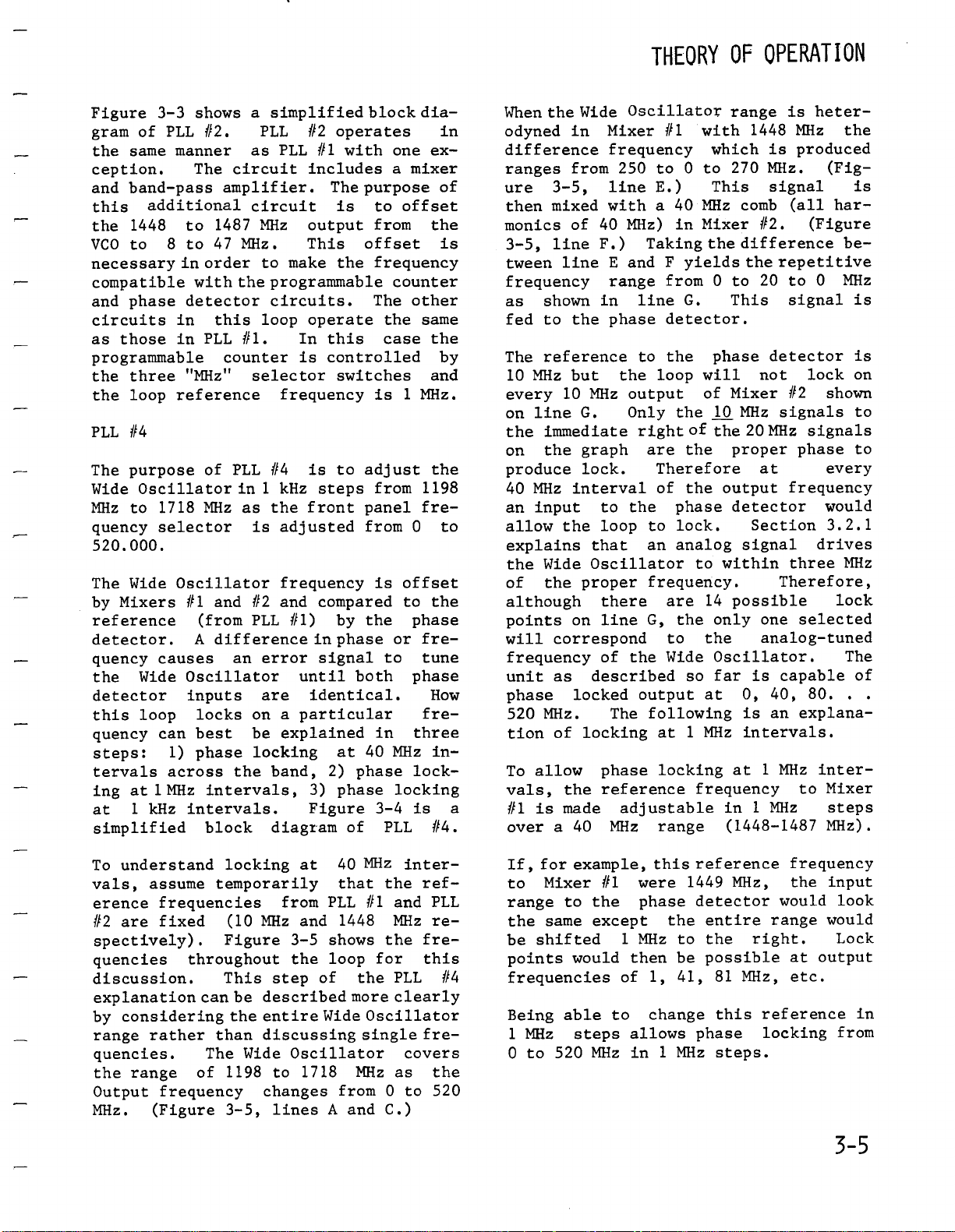
The
WideOscillator
MHz
quency
520
The
byMixers
reference
detector
quencycauses
the
detector
thisloop locks
quency
steps
tervals
ing
at
simplified
3-3
shows
of
PLL
#2
same
manner
.The
band-passamplifier
additional
1448 to
to
phase
those
three
loop
#4
purpose
1718
to
selector
.000
.
Wide
Wide
can
:
atIMHz
1
kHz
8
across
1487
to
47
in
order
with
detector
in
thisloop
in
PLL
"MHz"
reference
of
MHz
Oscillator
#1
and
(from
A
.
difference
Oscillator
inputs
best
1)
phase
intervals,
intervals
block
a
.
PLL
as
circuit
circuit
MHz
MHz
to
the
#1
.In this
counter
selector
PLL
in1kHz
as
is
#2
PLL
an
error
are
on
be
locking
the
simplified
#2
operates
PLL
#1
includes
.The
is to
output
.This
make
programmable
circuits
frequency
#4
the
adjusted
frequency
andcompared
a
explained
band,
.Figure
diagram
the
operate
is
controlledby
switches
is to
stepsfrom
front
#1)
by
in
phase
signal
until
identical
particular
at 40
2)
3)
phase
block
with
one
a
purpose
offset
from
offset
frequency
counter
The
.
the
case
1
is
adjust
panel
from
is
offset
to
the
or
to
both
.
in
MHz
phaselock-
locking
3-4
of
PLL
dia-
ex
mixer
the
other
same
the
and
MHz
the
1198
fre-
0
the
phase
fretune
phase
How
fre-
three
in-
is
#4
in
of
is
to
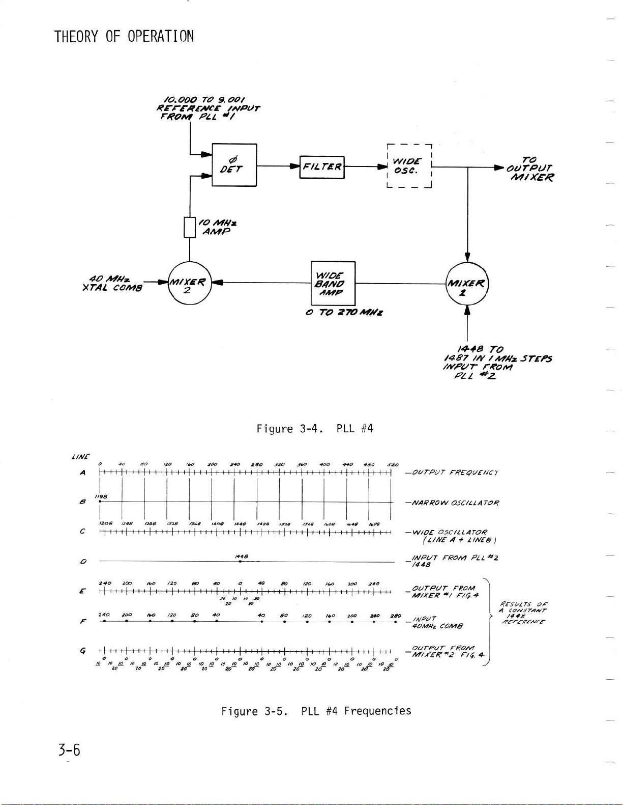
THEORY
Mixer
frequency
250
line
with
40
E
range
in
phase
MHz
G
.
graph
lock
.Therefore
to
loop
that
proper
there
line
of
described
locking
phase
reference
MHz
Oscillator
#1
to
E
.)
a
40
MHz)
and
line
to
loop
output
Only
right
are
of
the
to
an
frequency
G,
the
following
at
locking
range
in
F
from
detector
the
the
phase
lock
analogsignaldrives
are
the
to
Wide
with
which
0
to
This
MHz
Mixer
the
yields
0
G
.This
phase
will
of
10
of
the
the
the
.Section
to
14
only
the
Oscillator
so
far
at
1
MHz
frequency
When
odyned
difference
ranges
ure
then
monics
3-5,
tween
frequency
as
fed
The
10
.
a
.
every
on
the
on
produce
40
an
allow
explains
the
of
although
points
will
frequency
unit
phase
520
tion
To
vals,
#1
over
Wide
the
in
from
3-5,
mixed
of
lineF.)Taking
line
shown
to
the
reference
MHz
but the
10
line
immediate
the
MHz
interval
input
the
WideOscillator
the
on
correspond
as
lockedoutput
MHz
.The
of
allow
the
is
made adjustable
a
40
OPERATION
OF
range
1448
is
270
MHz
signal
comb
#2
difference
the
to
20 to
.
detector
not
Mixer
MHz
20
MHz
proper
at
output
detector
within
.
possible
one
analog-tuned
is
0,
40,
is
an
intervals
1
at
MHz
in
1
(1448-1487
is
heterMHz
produced
.(Fig
(all
har-
.(Figure
repetitive
0
signal
lock
#2
shown
signals
signals
phase
every
frequency
would
3.2.1
three
Therefore,
lock
selected
.The
capable
80
. . .
explana-
.
MHz
inter-
Mixer
to
steps
MHz)
the
is
be-
MHz
is
is
on
to
to
MHz
of
.
understand
To
vals,
erence
#2
spectively)
quencies
discussion
explanation
by
range
quencies
the
Output
MHz
assume
are
considering
rather
range
.(Figure
locking
temporarily
MHz
be
described
entire
discussing
Wide
from
3-5
the
step
Oscillator
to
lines
frequencies
fixed
.The
frequencychanges
(10
.
Figure
throughout
.
This
can
the
than
1198
of
3-5,
at 40
that
PLL
and
shows
loop
of
Wide
1718
A
MHz
#1
1448
for
the
more
Oscillator
single
MHz
from
andC.)
inter-
the
and
MHz
the
PLL
clearly
covers
as
0
to
ref-
PLL
re-
frethis
fre
the
520
#4
If,for
to
mixer
range
the
be
points
frequencies
Being
1
0
same
shifted
MHz
to
to
able
520
example,
#1
the
except
would
to
steps
MHz
this
were
phase
1
MHz
thenbe
of
1,
change
allows
in
referencefrequency
1449
MHz,
detector
the
entire
to
the
possible
41,
81
this
phase
1
MHz
steps
rangewould
right
MHz,
reference
locking
.
the
would
.
at
etc
input
look
Lock
output
.
in
from
3-5
Page 24
4O
Iii
THEORY
X
40
TAL
OF
.,oWx
COM8
OPERATION
/0
.000
R6F"E~4ENCE
FROM
TO9.
1
0
4L
00/
/NpllT
O~J
MIXED
TO
TP!/T
1448
/487
INPUT
PL
Figure
L
IN6
B
C
19
/198
/108
40
80
/20
/246 1268 /326
/60
T110
140
290
/368 /406 1448 1486
LINES)
E
F
240zoo
/60120
30/Oto
40
so
!O
n
26
1
3-4
320
.360
/J26
/J06 /606
61
0120/60
.
400
PILL
440
1640
2aozoo
#4
oleo
1686
"
S20
290
-Olrravr
-NARROW
-WlOE
LINE4t
INPUT
-
/448
_OUTPUT
MIXER
_
lI
r
40MNz
FREg41CIVCY
OSCILLATOR
OSCILLATOR
FROM
FROM
'6/
r-14
COMB
/W
FRgM
L
PLI-*.z
.4
TO
/WWlz
RESUL
A
STEP5
TS2,-
CONSTANT
l4ld
~PE~E~lNCE
l
{.
L~
0 0 0
Lo
10
L
20
10 ~! IOl0/O
2a 20
0 0 0 0 0 0 0 0 0
.
i. iii
lO lOlO1O l0/Ol0 /OL/O 1010AO
20
20
20
20
10
10 20
Figure
3-5
.
PILL
#4
10 /O
2J
0
lO la lO da
1(T
Frequencies
?Zr
OUTPUT
0
FROM
4-
Page 25
To
provide
the PLL
from
PLL
(10
.000
Wide
Oscillator
1
kHz
steps
locked
PLL
The
Narrow
MHz
Figure
gram
the
except
of
MHz
is
.
#3
purpose
Oscillator
.
3-6
of
same
that
programmable
a
output
combined
crystal
duces
signal
it
erence
a2MHz
is
compared
is
.Anydifference
nals will
which
tor
is
(VCO)
#4
#1
phase
phase
is
locking
detector's
adjustable
to9.001 MHz)
frequency
in
order
of
PLL
#3 is to
at a
PLL
showsa
#3
manner
it
from
in
simplified
.
This
as PLL
doesnot
the
a
mixerwith
controlled
difference
fed
to a
to a 2
produce
applied
to
to
correct
.
to
frequency
counter
Narrow
signal
phase
an
the
the
in1kHz
in
1
This
causes
to
keep
stabilize
block
loop
operates
#1
and PLL
require
.
Oscillator
a
.This pro-
signal
detector
MHz
crystal
in
the
input
error
Narrow
frequency
steps,
reference
kHz
steps
the
change
the
loop
of
1198
dia-
the
use
1198
The
1200
MHz
.This
where
ref-
sig-
voltage
Oscilla-
error
in
the
in
#2
With
VCO
of
a
O
volt
Figure
therefore
is
unchanged
racy
not
ting
the
and
is
reducedbecause
now
signal
VCO
frequency
below
instrument's
locked
the
maximum
a
to
generator
(0
the
operation
except
crystal
of +5
the
RF
this
will
deviation
THFORY
deviation)
3-7,
controlled
V to -5Vwill
to
2
MHz
outputsignal
reference
OF
OPFRATION
input
the
the
output
of
frequency
the
is2MHz,
the
generator
reference
A modula-
.
shift0.5
signal
.
Since
is
the
output
be
FM modulatedwith
MHz
of
.5
.
MHz
to
accu-
cause
phase
the
is
above
the
of
CRYSTALREFERENCE
All
phase-locked
single
40
appropriate
?MHz
Xr.4[
lNOlIT
reference
MHz
crystal
multiplication
loops
frequencies
are
derived
source
by means
or
division
for the
from
of
TO
OUTPUT
MIXER
a
.
the
.
To
provide
crystal
detector
output
Ea'T
Moo
/,PI/
reference
in
of
.
r
FM
PLL
a VCO
modulation,
applied
#3 is
as
replaced
shown
in
to
the
the
with
Figure
Figure
2
MHz
phase-
the
3-7
3-7
/ZOO
.Wz
XTAL
PLL
Atx
rm
E
INOUT
#3
/NPUT
.
Figure
.
FM
Circuit
3-6
TO
.
AEwER
PL
/
Page 26
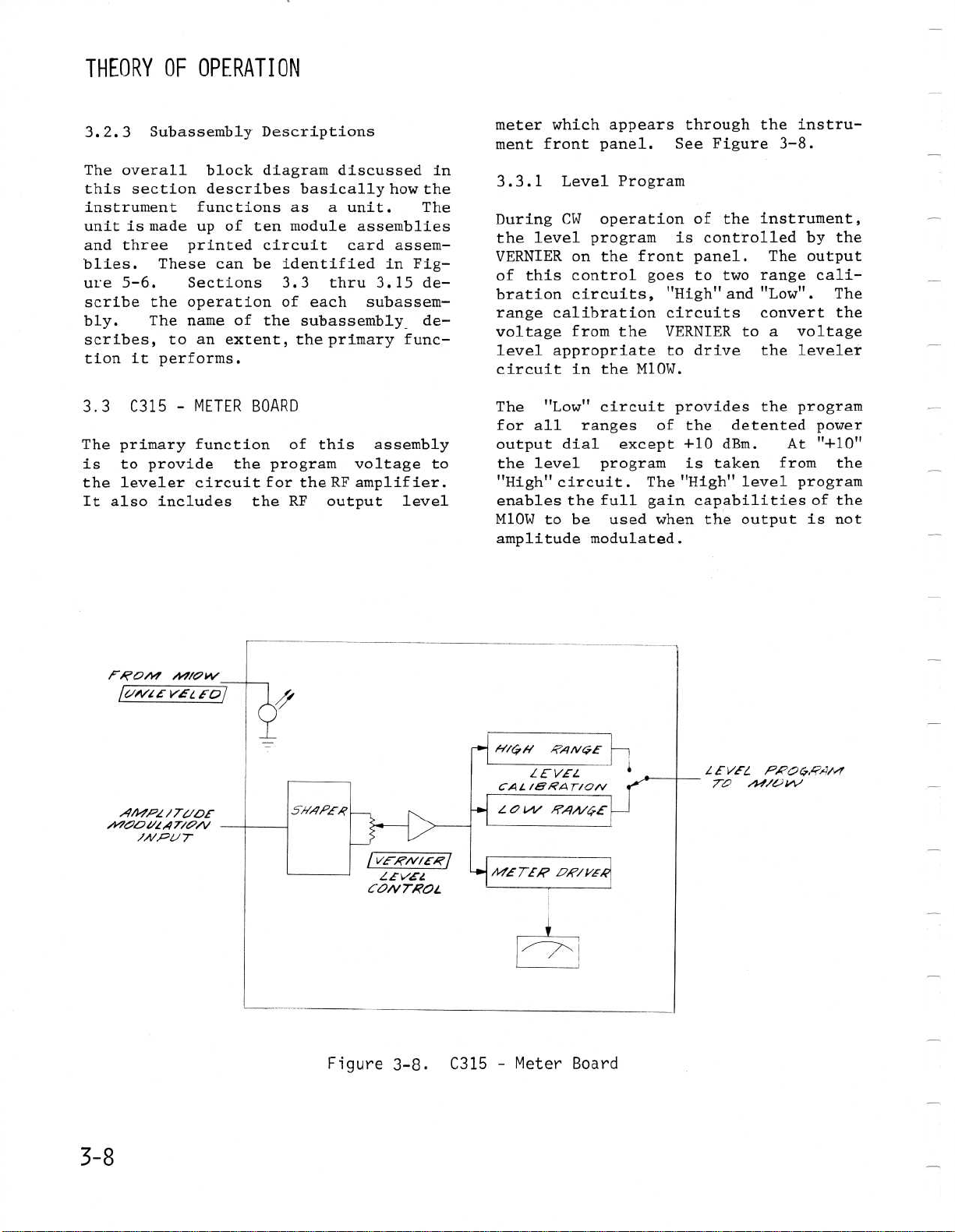
THEORY
OF
OPERATION
3.2.3
The
this
Subassembly
overall
sectiondescribes
instrument
unit
is
made
three
and
blies
ure
scribe
bly
.
These
5-6
.Sections
the
.Thename
scribes,
tion
it
performs
3
.3
C315
Theprimary
is to
the
It
provide
levelercircuit
also
includes
block
functions
up of
printed
can
operation
to
an
-
METERBOARD
function
Descriptions
diagram
discussed
basically
as
a
unit
ten
moduleassemblies
circuit
identified
be
3.3
of
of
the subassembly_de-
extent,
the
card
thru3.15
each subassem-
primary
.
of this
the
program voltage
for the
the
RF
RF
output level
amplifier
how
.
The
assem-
in
Fig
func-
assembly
in
the
de-
to
meterwhich
ment
3.3
front
LevelProgram
.1
DuringCW operation
the
level
VERNIER
of
this
bration
range
calibration
voltagefrom
level
appropriate
circuit
The
"Low"
for all
output
level
the
.
"High"
circuit
enables
M10W
to
amplitudemodulated
appearsthrough
panel
program
on
the
frontpanel
control
goes
circuits,
the
in
the
M10W
circuitprovides
ranges
dial
except
program
.The
the
full gain
used
be
the
.
SeeFigure
of
is
controlled
to
"High"and
instrument,
the
.
two
rangecali"Low"
The
circuits convert
VERNIER
to
drive
to a
the
.
the
of
the
detented
+10dBm
is
"High"
.
taken
level
capabilities
when
the
output
.
instru-
3-8
voltage
leveler
program
At
from
program
.
the
by
output
.
The
the
power
"+10"
the
of
the
is
not
Figure
3-8
LEVEL
TG
C315
.
-
Meter
Board
PF'Oc'5=f%trl
/N/UW
Page 27
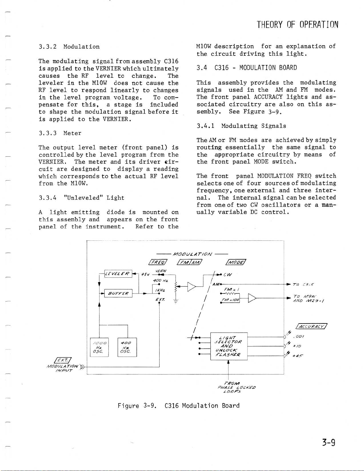
THFORY
OF
OPFRATION
3.3 .2
Modulation
Themodulating
is
applied
to
causes the
leveler
RF
in
pensate
to
is
applied
3.3 .3
The
controlled
VERNIER
cuit
which
from
.3.4
3
A
this
panel
in
the
level
the
to
level
for
shape
the
to
Meter
outputlevelmeter
by
.
The
are
designed
corresponds
the
M1OW
"Unleveled"
light
emitting
assembly
of
the
RF
the
signal
VERNIER
level
M10W
fromassembly
whichultimately
to
does
respondlinearly
programvoltage
this,
modulation
the
a
stage
VERNIER
signal
(front
the
level
meter
to
programfrom
and
to
display
the
its
actual
.
Light
diode
and
appears
instrument
.Refer
change
not
to
.To
is
.
driver
mountedon
is
on
.
cause
changes
included
before
panel)
a
reading
RF
level
the
front
to
C316
The
the
com-
the
cir-
the
it
is
M10W
description
circuitdriving
the
3
.4
C316
This
assembly
signals
The
front
-
MODULATION
used
in
panelACCURACY
sociatedcircuitry
sembly
3
The
routing
the
the
The
selects
frequency,
nal
from
.4 .1
AM
appropriate
front
front
.
one
.
See
Modulating
or
FM modes
essentially
panelMODE
panel
one
of
one
The
internal
of
two
Figure
four
external
uallyvariableDC
for
this
provides
the
are
3-9
Signals
are
circuitry
MODULATION
sources
signal
CW
oscillators
control
an
explanation
light
BOARD
the
AM
and
lights
also
.
achieved
the
same
switch
and
can
on this
by
.
FREQ
of
three
be
.
.
modulating
FM modes
and as-
by
simply
signal
means
switch
modulating
inter-
selected
oraman-
of
.
as-
to
of
MOGUL
/NPUT
AT/ON
Figure
3-9
FROM
PHASELOCKEO
L
OOiL5
.
C316
Modulation
Board
Page 28
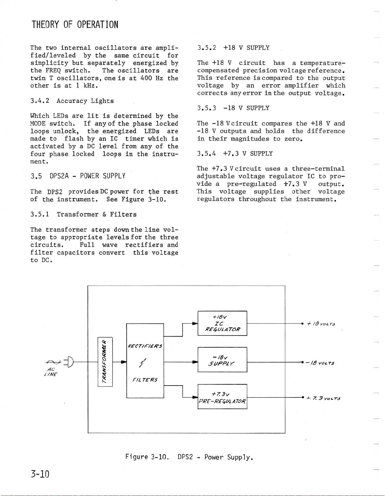
THEORY
The
two
internal
fied/leveled
simplicity
the
FREQ
T
twin
other
3.4 .2
Which
MODE
loops
made
activated
four
ment
3
.5
The
of
oscillators,
is
AccuracyLights
LEDs
switch
unlock,
to
phase
.
DPS2A
DPS2
the
instrument
OF
OPERATION
oscillators
by
the
but
separately
switch
at
are
.
.
1
kHz
.
lit
If
any
the
flashby
by
a
DC
locked loops
-
POWERSUPPLY
provides
.
same
The
oscillators
one
is at
is
determinedby
of
the
energized
an IC
level
timer
from
in
DC
power
See
Figure
are
ampli-
circuit
energized
400
Hz
phase
LEDs
which
any
of
the
instru-
for
the
3-10
for
are
the
the
locked
are
the
rest
.
by
is
3
.5 .2
The
compensatedprecision
This
voltage
corrects
3
.5.3
The -18
-18
in
3.5.4
The
+18V
+18
V
circuit
reference
by
any
error
-18
V SUPPLY
Vcircuitcompares
V
outputs
their
+7
magnitudes
+7
.3
.3 V
circuit
V
SUPPLY
iscompared
an
error
in
and
holds
SUPPLY
uses.a
has
voltage
amplifier
the
to
zero
output
adjustablevoltageregulator
videa pre-regulated
This
voltage
supplies
regulatorsthroughout
i-7
the
a
temperature-
reference
to
the
output
which
voltage
the+.18Vand
the
difference
.
three-terminal
.3
other
IC to
V
pro-
output
voltage
instrument
.
.
.
.
3.5 .1
The
tage
circuits
Transformer
transformersteps
to
appropriate
.
Full wave
filtercapacitors
to DC
.
AC
lNE
L
&
Filters
down
levels
convert
the
line
for
the
rectifiers
this
vol-
three
and
voltage
4/8voc
-lBvoc
rs
rs
3-10
Figure
3-10
.DPS2
-
Power
Supply
-f-7.
3
vocrs
.
Page 29
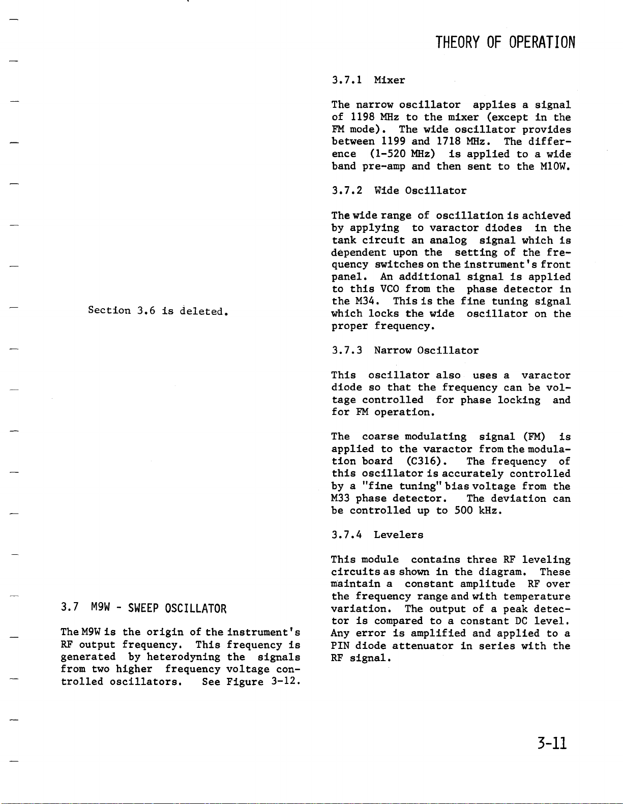
3.7
.1
Mixer
The
narrow
of 1198
FM
between
ence(1-520
band
mode)
pre-amp
MHz
.
1199
THEORY
oscillatorapplies
to
themixer
The
wideoscillator
and
1718
MHz)is
and
then sent
OF
(except
MHz
.
applied
to
OPERATION
a
signal
in
provides
The
differ
toawide
the
M10W
the
.
Section
3.6is
deleted
3.7 .2
Thewide
by applying
tank
dependent
quency
panel
to
the
.
which
properfrequency
3.7.3
This
diode
tage
for
The
applied
tion
this
by a
M33
be
WideOscillator
range
circuit
switches
.
An additional
VCO from
this
M34
.
locks
Narrow
oscillator
so
controlled
FM
operation
coarse
board
oscillator
"fine
phasedetector
controlled
that
to
upon
This
the
tuning"
an analog
the
modulating
(C316)
of
oscillation
to
varactor
the
onthe
the phasedetector
is
the
wide oscillator
.
Oscillator
also
the
frequency
for
.
varactorfrom
.
is
accuratelycontrolled
bias
.The
up to
diodes
signal
setting
instrument's
signal
fine
tuningsignal
uses
phase
signal
The
frequency
voltage
deviation
500 kHz
is
achieved
in
which
of
the
front
is
applied
on
a varactor
can
be
locking
(FM)
the
modula-
from
.
the
is
fre-
in
the
vol-
and
is
of
the
can
M9W
3
.7
TheM9W
RF
output
generated
from
two
trolled
-
SWEEP
is
the
frequency
by
higher
oscillators
OSCILLATOR
origin
heterodyning
of
the
.
This
frequencyvoltage
.SeeFigure
instrument's
frequency
the
signals
con-
3-12
is
.4
3
.7
This
circuits
maintain
the
variation
tor
Any
PIN
RF
.
Levelers
module
frequency
is
compared
error
diode
signal
contains
as
shown
a
.
The
is
attenuator
.
in
constantamplitude
range
amplified
and
output
to
a
diagram
of
a
and
series
RF
peakdetec-
DC
applied
three
the
withtemperature
constant
in
leveling
.
These
RF
over
level
to a
with
.
the
3-11
Page 30
THEORY
OF
IX-ROM
//134
Fl~OM
OPERATION
M3~
-
I
AlN
.,-/
7%1411N,~
C311o
OC-
BOA
rROM
4NALO4
`ROlAM172
WIDE
OSCILLATOR
NAfTR0W
OSCIG
Ro
LATOR
r!/WIWG
I
ll-99
1199
L
t
£
1/E[
-/718
MHz
Er~'t
ERS
F~
1011z
ro
ro
/-"a
rO
1'r3q
.0/o
/133
w
-'tRX
M10W-6
3
.8
mainfunction
The
amplify
to
to
a
level
+13 dBm
constant
the
widefrequency
programmable
.
A
amplitude
-
OUTPUTAMPLIFIER
of
the
RF
leveler
range
light driver causes
light
exceeds
See
3.8
This
band
RF
to
Figure
.1
Amplifier
section
amplifier
by about
glowwhen
its
proper
3-13
.
is
23 dB
a
four-transistorwide
which
.
Figure
the
M10W
signal
from
between
circuit
maintainsa
outputsignal
.
The Unleveled
front
the
the
leveler
operating
can
increase
3-12.M9W
module
the
-7
circuit
range
is
M9W
and
over
panel
.
the tronic
Sweep
3.8.2
The
Oscillator
Leveler
leveler
uses
ferentialamplifier
attenuator
from
the
is
compared
the
differential
.The
RF
output
to
a
controlcurrent
uator
viates from
signal
to be
In
response,
reference
addition
tude
(C315)
.If
to
the
the
decreased
to
the
control
by varying
comes
.
the
PINdiode
providing
leveler
of
a
peak
detector,
and
peak detector
The
(or
the
resulting
AM)
which
PIN
RF
.
DC
amp
to
detector
reference
causes
or
increased
a
allows
the
RF
DC
reference
the
the
from
dif-
a
PIN
diode
is
level
referenceby
supplies
diodeatten-
output
level,
input
the
.
flat
frequency
for
elec-
outputampli-
.
meter
board
fed
the
de-
the
The
Page 31

,PF
/Yl9
FROM
kv
PIN
O/OOE
ATTENUATO
"
S
UNG
FVELEO"
L
AS
NT
0
.4l
.q
VER
WlOE
AMPG
BANp
FlEQ
l
401r1-EREN7
AMP
1A1
-
s
(''EFERENCE)
THEORY
lwCi/VlTO.Q
OIOGE
OF
OPERATION
-~
O4/~rPUT
MO
STEP
AASSIYE
ArrrArkA1TOR)
3
.8 .3
When
circuit
"Unleveled"
differential
the
is
would cause
be
at
its
the
levelingcircuit
effective
which
driver,
of
pears
3
This
One
current
.9
are
through
M172
module
is
linear
are
frequency
peating
from
from
is
M9W
+7
0 to
shaped
Sweep
every
V
putting
the PIN
high
or
.
The
applied
adequate
for
the
the
-
SWEEP
provides
from
goes
40
to
-8
520
MHz
to
linearize
Oscillator
TOL/LINT
MJETENP
B0
Figure
LightDriver
amp
out
diode
lowresistance
can
above
to
to
voltage
the
turn
indicator
front
DRIVE/DAC
two
0Vto
from
MHz
V
as
0
;
the
the
.
The
.
ON
.4k'D
.
in
3-13
the
M10W
leveler
a voltagewhich
attenuator
limit,
no
longer
levels,
unlevel
on
a
light
source
which
panel
output
to 39
.
-5
voltages
V
as
MHz,
othervaries
frequency
second
the
VCO
goes
voltage
in
to
be
ap-
the
re-
the
F
.QOM /LIFTER
-
.
LEVEL
CONTROL
Output
Two
Amplifier
digital-to-analog
programmed
Indicator
MHz
voltage
section
vides
Since
on
verted
The
is
the
the
the
100's
when
analogtuningsignal
"shaped"before
oscillator
DC
amplifier
smaller
by
a
tude
inputs.Shaping
compensates
in
capacitance
in
the
oscillator
BGARO
by
switches,
.
of
the
repeating
state
the
.
the
front-panel
provide
This
is
shaped
module.A
0
- 40
of
the
20's line
line,
100's
the
line
driving
The
shaper
which
amplifies
factor for
this
for
the
non-linear
of
the
circuit
converter
Lever/
the
0
to
in
the
third
MHz
DAC
voltage
depends
20's
is
from
the
is
an
smaller
analog
line
is
high
.
the
M9Wwide
inverting
the
input
magni=
voltage
change
varactordiodes
.
ICs,
520
next
pro-
.
in-
M172
3-13
Page 32

THEORY
OF
-A
WW~
Z=
<V0
O
CC
rrZ
L-
O
2QO
OU_cr
jr
EiJ
W
Zm
y~7
E-
CC
>>0
a
z
~
A
OPERATION
10
2
20
Q
r
O
O
CC
40
O
80
100
200
400
800
2
4
8
TO
TO
MHz
STEPS
WIDE
VCO
3
.10
M29-1
The
M29-1
verter,
a
phase
module
rent
source
frequency
(See
Figure
2
MHz
is a
the
lock
includes
of) a
out
.
-
FM
voltage
output
reference
a
which
square
3-15
.)Zero
Figure
REFERENCE
to
frequency
of
which
in
is
the
voltagevariable
feeds
(determines
wave
oscillator
volts
M33
in
3-14
used
.
yields
con-
The
cur
the
.
as
.
M172
Sweep
3
.10
Thiscircuit
and
Drive/DAC
.1
CurrentSources
a negative
provides
source
botha positive
of
current
The
.
Page 33

THEORY
OF
OPERATION
~L
Sv
MODOLATINfr
S1GN'A
positive
negative
eous
currents
The
change
proportional
tage
to
the
mayvary
circuit
is
current-out
L
source
source
in
both
in
output
to
the
circuit
between
designed
vs.voltage-in
is
so
-5
that
current
change
.
Figure
referenced
the
sources
in
The
input
and
+5
for
a
very
curve
3-15
to
instantanare
equal
is
directly
input
voltage
volts
.
linear
.
.
the
vol-
The
M29-1
.
-
FM
Reference
a
decreasing
wave
input,
triangle
Changing
by
changing
module,
capacitor
hysteresis
oscillation
wave
the
magnitude
changes
charges
points
changes
voltage
therefore,
.
the
input
the
and
thus
.
l.S-2.SMf/z
ramp
.Forasquare
the
output
of
the
"currents",
voltage
rate
at
discharges
the
frequency
which
to
to
is
a
the
the
the
of
3
.10
.2
The
square
the
combination
hysteresis
verts
The
a
triangle
switch
is
fed
The
integrator
switch
wave
applied
a
square
to
the
Positive
increasing
and
negative
Oscillator
wave
switch
square
to
produce
back
and
to
a
to
current
capacitor
constant
voltage
wave
wave
the
is
capacitor
the
output
of
an
.
The
to
causes
the
integrator
made
current
signal
produced
is
integrator
integrator
a
triangle
the
square
up of
.
The
switch
to
be
hysteresis
wavewhich
.
a
current
square
causes
applied
.
current
ramp
on
produces
the
capacitor
constantcurrentproduces
and
con-
wave
by
an
3
.11
M30
-
CRYSTAL
This
module
a
.
cies
its
and
in
at1kHz,
harmonics,
1440
the
instrument
produced
andaseries
See
Figure
3 .11
.1
This
crystal
the
accuracy
circuits
perature
stability
oscillator
in
all
M30modules
supplies
MHz
by
a
of
3-16
40
MHz
oscillator
of
in
the
compensated
.
A
output
1
to
40
dividers
.
Oscillator
the
levelercircuit
REFERENCE
reference
MHz,
1200
the
2
MHz
phase
.These
MHz
crystal
frequency
instrument
level
.
MHz,
(from
and
is
.
for
to
frequen-
40
MHz
120
comb)
locked
loops
signals
oscillator
multipliers
the
heart
determining
It is tem-
frequency
causes
be
the
and
are
.
of
the
same
3-15
Page 34

THEORY
OF
OPERATION
21WHz
/MHz
/
A042
40
COME
120
COMA
/440
Milt
MWs
MVL
?p0M.fis~
3
.11
The
duced
"divideby
put
optionalhigh
frequency
in
kHz
3
.11
The 40 MHz CW
erator
From
and
tor
is
the
3
.12
The
from
DIVIDERS
.2
frequencies
by
a
for
the
Figure
and
1
MULTIPLIERS
.3
which
the
40
applied
.
A
sample
also
1440
M31A
input
the
fed
MHz
front-panel
series
4"
is
3-16
kHz
MHz
to
Figure
below
produces
phase-
stabilityreference
further
to
outputs
is
produces
comb,
to
another
of
to
a
output
-
kHz
this
40 MHz
of
TTL counters
lockedloop
divided
provide
.
fed
to
the
120
harmonic
the 120
filter
.
STEPS
module
"kHz"
the
a harmonic
is
3-16
are
.
10
MHz
in
.
as
shown
the
1
MHz,
"comb"output
MHz
is
selected
genera-
MHz
comb
output
which
provides
BCD
the
switches
.
proout
the
This
gen-
data
(to
M30
A
2
.
-
Crystal
the
output
where
kHz
to
output
of
3
.12
The output
Voltage
tuneablefrom9.001
.12
3
Including
permitsaccurate
VCO
Frequency
signal
applied
(IC9)
divided
the
of
the
right
Sk
switches
333
.333
is9.667
the
M31
.1
.2
tuning
.
result
phase
Reference
of
frequency
is
the
.If
MHz,
is
VCO
frequency
ControlledOscillator
PHASELOCKED
the
voltage
Detector
from
to
one
A
sample
by
the
is
detector
the
decimal
is
(10
number
for
MHz
shown
VCO
programmability
the
Crystal Reference
input
Programmable
applied
indicated
FREQUENCY
the
example,
.
The block
Figure
in
is
to
10
LOOP
inaphase-locked
comes
circuit
of
the
the
of
to
.Any
point)
MHz
generatedby
.000
from
phase
VCO
the
difference
.The
-
Sk
by
is
the
diagram
3-17
which
MHz
.
.
the
Phase/
A
1
.
detector
input
Divider,.and
other input
kHz),
the
set
M31A
.
a
is
loop
The
kHz
is
is
in
3-16
Page 35

"K
SWITCHES
HZ'
THEORY
1
KHZ
REF
OPERATION
OF
phase
applied
produces
detector
VCO
.
The
the
phase
so
that
locked
3
.12
.3
In
order
erly,
the
is
The
at
the
count
the
VCOfrequency
the
number
divider
its
countreaches
is
switches
is
set for
divide
10,000)
to
the
(1
kHz)
MHz
.
or
frequency
to
the
phase
an
error
output,
system
to
and
the
the
frequency
output
1
kHz
PROGRAMMABLE
for the
M31A
divider
by
set
on
counts
input
.
the
For
222
and
number
example,
.500
puts
MHz,
by 9,500
.
Therefore,
phasedetector
only
if
the
Figure
in
detector
voltage
which
is
controls
stable
error
frequency
reference
DIVIDER
to
perform
is
designed
(10,000-Sk)
the
"kHz"switches
the
number
out
10,000
(count
shown
this
the
.
on
if
the
circuitwould
from
variable
wouldbe correct
VCO
output
SK
the
at
the
only
is
is
signal
to
where
of
a
pulse
The
starting
the
instrument
were90
=
SETTINGOF
3-17,
signals
inputs
phase
when
zero,
phase
prop-
divide
cycles
when
"kHz"
500
input
500
the
.
S
to
'KHZ°SWITCHES
M31A
k
.
-
kHz
.12
3
.4
When
the
LED on
and the
flash
A
window
level
detector
exceeds
power
the
flasher
Board
Steps
UNLOCK
the
phase-locked
front-panel
.
detector
which
to
the
is
applied
.
INDICATOR
loop
top
of
the
module
ACCURACY
monitors
is
being
the
VCO
fed
.
normal operating
to
the
module
circuit
on
from
If
the
is
unlocked,
will
lights
the
voltage
the
the
voltage
light
Modulation
light
will
phase
range,
and
3-17
Page 36

am
THEORY
3
.13
The
ence
setting
block
outputrange
repeats
the
of
M32A
setting
(1448
der
panel
R wouldbe
Remainder
M32A
3
.13
The output
Voltage
VCO
analog
is
phase-locked
VCO,
phase
3
.13
A
sample
the
Reference
quency
shaped
Programmable
OF
M32A
M32A
the
provides,
frequency
on
diagram,
itself
frequency
outputrelates
+
R)
of
dividing
is
would
.1
VCO
is
coarsely tuned
output
result
the
detectorand
PROGRAMMABLE
.2
of
1440
MHz signalfrom
of
into
OPERATION
-
MHz
STEPS
for
the
which
the
Figure3-18
is
with
(S.)by
MHz),
set,
Controlled
phase-locked
formexample,
13(333
of
13)
then
be
of
the
of
of
loop
the
VCO
producing
from8to
TTLpulsesand applied
Divider
corresponds
"MHz"
1448
switches
the
where
Sby 40
.The output
1448+
M32A
the
including
.In
Programmable
output
47
switches
to
1487
every
.
to
the
equation
R
is
.If
+
.000
13
is
Oscillator
by
2122
.Pine
addition
loop
DIVIDER
a
difference
MHz,
.
M34,
a refer-
.
.)
The
MHz,
40
MHz change
specific
Any
"MHz"
(Output
the
Remain
the
for
333
40
=8with
of
1461
=
produced
.
the
repeating
the
VCO
includes a
Divider
is
mixed
the
which
crystal
is
to
the
(See
M32A
which
switch
front-
.000,
the
MHz
by
This
tuning
in
to
the
with
fre-
then
to
the
to
starting
count
effectivedivisorvaries
When
frequency,
resetpulserate
3
.13
=
One
reset
Divider
a
.
a
a
.
fixed
Reference
is
difference
detector
any error
phase
If
high,
output becomes more
increasing
tuning
frequency
low,
will
frequency
attenuatorbetween
circuitand
gain
constant
range,
minimized
Programmable
the
count
varies from
the
VCO
PHASE
.3
input
reference
a voltage determined by
.
the
the
tend
of
to
pulse
.
The other
.
The phase
inputs,
VCO output
for
capacitance
.
reverse
to
error
the
phase-locked
over
allowing
.
Thus,
.
is
running
the
will
DETECTOR
the
from
signal
phase
in
and
in
the
example,
the
If
the
occurs
maintain
.
the
VCO keeps
the
Divider
as
the
0
to
from
at
the
Programmable
1
MHz
be
phase
VCO
VCO
A
the
detector
the
is
VCO frequency
frequency
the
and
voltage-controlled
the
programmed
Programmable
input
from
detector
at
usedto
phase
negative,
varactor
lowering
frequency
.
Thus,.the
zero
phase
the
loop
loop
noise
is
the
47
.
the
phase
open-loop
relatively
frequency
the
as
starting
39,
a
detector
detector
the
to8.
correct
Divider
is
the
1
MHz
Crystal
output
the
phase
correct
is
too
thus
diode
the VCO
is
too
loop
to be
or
or
The
Divider
the
8-47
each
The resetpulse
Divider,
The startingcount
Divider
Memory,
time
of
the
phasedetector
the
starting count
controlled
the
correct
"S,
:h"
setting
counts
MHz
a
count
the
effective
.
is
selected by
which
"R"
.
is
This
3-18
the
input
is
programmed
pulses,
of 47 is
applied
.
of
of
information
"R"
falling
to
By
the
Programmable
divisor
the
Programmable
a
is
then
edges
resetting
reached
one input
controlling
canbe
Read Only
to
provide
for
each
applied
of
3
.13
.
When
the
and the
flash
A
window
level
detector
exceeds
power
the
Board
UNLOCKEDINDICATOR
.4
the
phase-locked
LED on
.
which
flasher
.
top
front-panel
detector
to
the
is
applied
circuit
is
the
normal
of
being
VCO
to
loop
the
modulewill
ACCURACY
monitors
fed
.
operating
the
from
If
module
the
is
unlocked,
lights
the
the
the
light
Modulation
light
will
voltage
phase
iroltage
range,
and
Page 37

1440
MHZ
THEORY
OF
1448-1487
(1448+R
OPERATION
MHZ
~/20
/ZOO
COMB
BAS
/.X-2.
M//:
Mllz
VCO
9W)
FlrOM
16429
M30)
.T
u
A'EFEFrENCE
Figure
Ml
XEI?
SW/
-7
LEvZLER
rcm
0
.av
3-18
REPEATING
ANALOG
.
M32A
-
MHz
VAA
7
1ABL
/POUF
A'EFE,PFNCE
IMR4V
Steps
r
E
TUNING
r11-
TCR
TO
NARROW
OSC1LLA
/N
M9W
TOR
2
,-?OM
MNz
M30
+Z3vFOR
AND
Figure
AM
3-19
CW
1WGOE
.
.S
M33
NarrowOscillator
-
Lock
3-19
Page 38

THEORY
3 .14
TheM33
for
which
lator"
phase
"reference"
3
.14
Thiscircuit
quency
represents
too
is
tector
which
integrator
row
3
.14 .2
OF
M33
-
is
the
in
the
detector,
.1
PhaseDetector
to
the
the
high,
puts
filtered
is
and
oscillator)
Mixer
OPERATION
NARROWOSCILLATOR
part
VCO
M9W
switch
compares
variablefrequency
VCO
for
out
The phasedetector
UHF frequencies
1200
MHz CW
frequency
the
to
of
this
precisely
VCO from
the
.
which
phasedetector
variable
the
1198
of
a
phase
is
the
"Narrow
.
The
M33 includes
mixer
and
.
See
thereference
output
example,
a
more
applied
to
positivevoltage
and
inverted
to
lower
the
can not
so
the
VCO
Thisprovides
is
the
variable
.The
signal
same
MHz
as
W/DL
.
nw9
the
w
VCD
LOCK
locked
Oscil-
an electronic
Figure
3-19
which
IF
.
the
the
phasede-
by
the
VCO
(nar-
frequency
operate
is
mixed
an
offset
input
deviation
from
2
MHz
deviation
loop
fre-
VCO
with
.
an
at
of
is
3
.14
.3
Reference
This
switch
a
selects
for
instrument
hex
the
guarantee
to
3
circuit,
CW operation
(1
.5-2
inverter
the
.15
on
the
either the
.5
MHz)
.The
reference
that
phasedetector
M34
-
WIDEOSCILLATORLOCK
Thismoduleprovides
gramfor the wide oscillator
.
Figure
M34
.
signals
module
3-18
VCO
cated
and
to
3-20tis
The
at
to
3-19
1198
on
all six
letters
the
the
MHz plus
Switch
controlled
instrument
2
MHz CW reference
or
the
for
FM
operation
referenceswitch
to
electronically
signals
TTL
levels
.
the
the
block
A
thru
associated
graphs
.
A
thruFin
TheM34 phase
the
front
the MODE
by
front panel,
FM reference
of
uses
route
as
well
will
fine
diagram
be
tuning
in
the
as
M9W
of
F relate
points
in
Figures
locks
frequency
panel
indi-
switches
the
a
to
fed
pro-
.
the
the
the
the
.
3-20
Figure
3-20
F.P
.
!/n1L
OG'K
FLASHER
iY19W
WIDE
OSC/G
L
raR
4
TOiH9
.
M34
-
Wide
Oscillator
Lock
W
Page 39

4194
0
AN
MNz
MNz
MHz
THFnRY
1718
/b98
/S93
/498
.
/398
1298
1198
/467
1449
270250--
210
280
2401
200
160
/20
170130
-90--
SO
90
40
O
-
4
~
I
?Oo
/70
SO
/o
/Zo
40
0
70
1212
g12
/so
OF
OPERATION
.200
280
The
quency
The
VCO
from
of
ence
The
positive
detector
frequency
the
frequency
which
information
tor
.
In
set
circuit
eral
3
auxillarycircuits
.15
.1
phase
frequency
theM31
the
M31
tion
of
.)
phase
the
wide
frequency
of
retains
for
addition
andthe
PhaseDetector
detectorcompares
to
.(Refer to
for
this
10
detector
negative
or
oscillator
until
are the
integratorserves
for
the
phase
detector
O
BO
Figure
offset
the
use
to
phase
circuit
VCO
the
by
the
a
to
frequency
the
phase
frequency
detector,sevare
the
referencefrequency
the
a
more
.000
detailed
-9.001
output
to
ultimately
voltage
higher
both
same
as
inputs
frequency
a
low
.
110
/00
3-21
/60
.
M34
converts
lower
fre-
error
detec-
off-
included
the"offset"
description
descrip-
MHz refer-
goes
drive
lower
or
to
the
phase
.
pass
filter
The
OUTPUT
.
in
200
-
;
140
Signal
3.15 .2
The
verted
phase
by
mixer
Refer
for
Mixer
with
quency
frequency,
270
42
MHz
graph
the
the
of
mixer
difference
(assuming
190
300
F-R10Ue/VC)
Frequencies
Frequency
VCO
error
to a
detector
mixer
#2
to
descriptions
41
the
(1448
MHz
.This
where
comb
.For
D
comb
desired
m
;xPr
,#
BZO
3(0
,
MNz
information
frequency
.
#1, a
and
270
a 10
Figures
heterodynes
"MHz
+
R)
11448
it is
heterodynedwith
in
Figure
frequency
output
# 2
.
2
will
as
the
"kHz"
400
Offset
This
MHz
MHz
3-20,
of
steps"
MHz
+
signal
any
Tf
produce
Ghown
switches
-~t~{-
440
Circuit
useable
conversion
low
low
3-21
signals
the
VCO
reference
.The
R-VCOJ,
is
sent
output
3-21
which
(
below
the
loop
in
.~-_
4,510
500
must
pass
pass
and
.
frequency
difference
is
to
frequency
shows
will
20
is
a 10
Figure
are
-ma
y
1
.00
be
con-
by
made
is
filter,
filter
3-22
fre-
below
mixer
the
only
yield
?liz)
locked,
MHz
3-21
set
for
the
.
40
3-21
Page 40

THEORY
/298
68
0-
/6
160
0
0
Figure
000)
.
F
fora
not 000
MNz
.000-
NINZ
170
.000
MNz
9
.99
MNz
MHz
9
995-
MHz
R9
Figure
OF
1019.000
.T
/0
10
.9
100.000
3-22
case
.
OPERATION
I
-
-I
.M34
3-22
when
OUTPUT
L
04'r,-417-E
-
Frequencies
(Expanded)
shows
the kHz
FREQUENCY
.PEQUENG'Y-MNZ
signals
-
MHz
switches
filterafter
The
the
outputs
frequency
/OQ
003
information
the
filterpasses
able
to
allowed
loop
is
10
MHz
loop
related
3
.15
.3
"speed-upcircuit"
The
the
phaselocked
The
the
output
M9W
faster
"unlock"
The
voltagefrom
leveler
condition
it
sends
cuit
.
/00
.005
-
The
levelercircuitmaintains
input
by
controlling
input
input
from M9W
to
MHz) is
A
thru
are
a
DC reference
The
leveler
attenuator
put and
of
signal
.
capture
for
locked
to
further
Auxillary
of
to
cause
by
the
voltage
of
a
voltage
amplitude
the
peak
which
mixer
the
When
analog
spurious
analogvoltage
amp
the
the
phase
detected
circuit
#1
mixer
the
mixer
containing
the
up
over
tuning)
the
filter
#2
exceptthe
theVCO
unit
to
20
the
20
.
decreases
is
MHz
eliminatephase
signals
Circuits
is
activatedwhen
loop
becomesunlocked
this
circuit
the
VCO
is
to be
.
monitorsboth
phasedetector
to
detect
an unlocked
M34.Whenunlock
to
the
flasher
to
the
phase
the
amplitude
wide
oscillator
detector
in
is
and
the
controls
between
compared
levelercircuit
a
the
.
blocks
unlocked
MHz
Once
.
sent
the
and the
occurs,
a
constant
detector
of
.The
(about
PIN
VCO
all
lower
error
(to
range
the
locked
tuned
tuning
cir-
the
diode
in-
be
to
.
to
10
to
.
Page 41

4
.1
INTRODUCTION
The
purpose
the
following
that
the
Model
meets
agraph
tests
be
list
test
a
Critical
of
4-1
cept
ment
all
tails
The
top
performance
its
published
1
.2)
consist
verified,
of
equipmentrequired
procedure
simplifiedsetup
specifications
test
equipment
of
RecommendedTest
as
detailed
apply
other
Signal
and
to
test
are
omitted
bottomcovers
of
the
performance
paragraphs
3000
Signal
specifications
.Individual
of
:
the
the
method
including
drawing
are
settings
performance
equipmentoperating
.
Generator
installed
tests
.
All
testsin
is to
Generator
performance
specification
of
testing,
andadetailed
in
some
.
for
each
listed
Equipment
of test
test
should
in
procedures,
have
of
the
for the
verify
(par-
cases
item
Table
.
Ex-
equip-
de-
its
tests
to
SECTION
PERFORMANCE
can
be
performedwithout
internal controls
power
tion
lation
maintained
or
performance
a
after
Signal
ambient
A copy
(PTR)
section
the
performance
out and
incoming
as
ing
basic
of
to
the
Signal
2
for
details
.
The
at
60
Hz
throughout
test
a
two-hour
Generator
temperature
of
the
is
provided
for
convenience
performance
tests
used
inspection
a
guide
.The
the
for
PTR
controlsettings
tests
refer
.
Generator
of
line
115
Performance
of
as
routineperformance
lists
voltage
or
procedures
minimum
in
range
at
the
.
a permanent
the
to
access
Before
electrical
230
volts
the
tests
warmup
a
+20
.
Test
the end
in
Model
It
can
or it
can
paragraph,
and
limits
this test
to
3000
4
TESTS
to
applying
see
instal-
should
±10%,
.The
are
begun
of
+30
record
of
recording
during
be
filled
record
be
test
test,
.
record
the
Sec-
be
50
the
0 C
this
for
used
All
.
INSTRUMENT
DigitalMultimeter
Distortion
FrequencyCounter
Function
Analyzer
Generator
TABLE
4-1
FOR
MODEL
10
VDC
Range
Range
Level
600
Range
Distortion
.
RECOMMENDED
3000
CRITICAL
:
t(0
:
5
:
to
:
10
ohm
:
>0
PERFORMANCE
REQUIREMENT
.07IR+0
Hz
to
525
Vp-p
load
.2
Hz
:
<1%
MHz
>25
sine
to
TEST
.02%FS)
kHz
wave
>25
kHz
EQUIPMENT
TESTS
into
RECOMMENDED
Keithley
HP334A
HP5300B/5303B
Wavetek
179
130
Page 42

PERFORMANCE
PowerMeter
ModulationMeter
Oscilloscope
Spectrum
PrecisionAttenuator
Pads
TESTS
Analyzer
TABLE
Range
Input
Accuracy
Range
Residual
ResidualAM
AM
Range
Sensitivity
Range
Display
10, 20,
:10
Level
:
:5 to
(quiet
(in CW)
Accuracy
:
DC
:500 kHz
:
30
FM
4-1
.
(Cont'd)
to
>520
MHz
:
-7 to
t1I
FS
>520
MHz
:
<100
Hz
room)
:
<0
.1%
:±(2%R+1IFS)
to2MHz
:
2
V/cm
to 1200
2
dB
log and
and
40 dB
+13
(rms)
(rms)
(AC
dBm
coupled)
MHz
10
dB
log
HP435A/8481A
AFM2
HP8554L/8552B/
Weinschel
Radiometer
Tektronix
5A18N/5B10N
141T
50-20,
and
50-40
D10/
50-30,
50-10,
WidebandAmplifier
Sweep/Signal
VSWR
Coaxial
Loop
4.2
SPECIFICATION
METHOD
Bridge
50
ohm
Probe
FREQUENCY
Range
Resolution
Short
Load
Range
Gain
Impedance
GeneratorRange
5
to
50
Type
BNC
See
RANGE
AND
RESOLUTION
1
MHz
1
kHz
A
frequencycounter
and the
modes
indicatorswitches
lector
digits
1
to
;
:
26 dB
:
525
dB directivity
N
female
Figure
to
520
frequency
between
(a
provide
:
1
to
MHz,
TEST
total
520
50
520
4-9
MHz
1
and 520
1
MHz HP8447D
ohm
MHz Wavetek
ohm Wiltron
50
.
1
selectable
is
used
resolution
MHzare
.Each
of
56)
kHz resolution
of
will
kHz
in
to measure
.
All
selected
the
digits
be
tested
.
steps
frequencies
.
the
by
front-panel
of
the
.The
HP11511A
HP11593A
frequency
in
frequency
0
through
CW
2001
60N50
range
and
lever/
9
AM
se-
kHz
4-
2
Page 43

EQUIPMENT
Frequency
PROCEDURE
Counter
HP5300B/5303B
1.Set the
FREQUENCY
MODULATIONMODE
MODULATION
MODULATIONFM/AM
OUTPUTVERNIER
OUTPUT
2.Connect
ohm
inputof
frequency
3.Observe
setting
steps
by1.00
9
specification
and
kHz
.Theforegoingprocedureverifies
step
to
of
verify
kHz
Signal
selector
FREQ
the
the
the
the
±1
Generatorcontrols
050
CW
(Inactive
(Inactive
Fully
attenuator
Signal
frequency
seven
frequencycounter reading
Signal
that
count
.
Generator
digits
Generator
the
for
+10
counter
.
FREQUENCY
frequencycounter
each step
PERFORMANCE
as
.000
MHz
in
in
Clockwise
dBm
RF
out
connector
.
Set the
increasefrom
the1kHz
follows
CW
MODE)
MODE)
CW
counter
.Increase
selector
reading
TESTS
:
to
the
to
in1kHz
increases
1
through
resolution
50
read
the
4
.3
FREQUENCYACCURACY
SPECIFICATION
Accuracy
4.Repeat
creases
kHz
step
for
mark
FREQUENCY
Ran_&e
050
050
050
050
001
0
.20
TEST
CW
FMxl
FMxl00mode
digits
is
each
in
.000-050
.000-050
.000-050
.000-059
.000-091
.000-520
and
AM
mode
indicated
equal
the
(MHz
the
.
of
the
applicable
Selector
)
.009
.090
.900
.000
.000
.000
modes
procedure
in
If
the
to
the
steps
Increase
per
the
actual
allowable
indicated
step
1
10
100
1
10
100
±0
.001%
2
hours
±(0
±(0
table
space
kHz
kHz
kHz
MHz
MHz
MHz
.001%
.001%
in step
counterfrequency increase
on
after
within
+10
+45
3
for
all
other
belowbeginningwith
increase
in
the
line
FrecLue
No
.
Digits
7
7
6
5
5 10
6
15
3
kHz)
kHz)
1
ncy
min
months
per
table,
of
the
Counter
Allowable
per
step
100
(Typ
.
of
step
place
PTR
1
.00
10
.00
100
1
.000
.000
.00
±0
calibration)
step
±1
a
.
Reading
Increase
±1
count
kHz
kHz
.0
kHz
MHz
MHz
MHz
.002%
the
count
check
after
in-
10
per
4-3
Page 44

PERFORMANCE
METHOD
EQUIPMENT
Frequency
PROCEDURE
TESTS
Counter
A
frequencycounter
In
CW
and
AM modes
derived
Signal
that
specified
Frequencyaccuracyin
accuracy
a voltage-controlledoscillator
of
in
FMx1
tionwith
mum
HP5300B/5303B
FREQUENCY
MODULATION
MODULATION
MODULATION
OUTPUT
OUTPUT
from
Generatorwill
the
crystal-controlled
limits
.
The
the
crystal-controlledoscillator
and
FMx100
a
DC
sinusoidal
Set
the
Signal
selector
MODE
FREQ
FM/AM
VERNIER
step
attenuator
allfrequencies
a
single
.
FM systemaccuracy
modes
modulation
modulation
used
is
crystal-controlled
be
tested
FM
modesdepends upon
will
signalequal
signals
Generator
to
measure
between
one
includes
addition
.
.000
CW
.
Frequencyaccuracy
to
as
MHz
at
oscillator
in
be measured
controls
040
CW
(Inactive
(Inactive
FullyClockwise
+10dBm
frequency
1
and 520
oscillator
frequency
operates
the
the
to
in
VERNIER
the
peak
follows
in
CW
MODE)
in
CW
MODE)
accuracy
to
FM
accuracy
accuracy
the
of
:
MHz are
.
The
verify
within
system
of
posimaxi-
.
2
.
Connect
Signal
3.The
kHz
of
4
.
FREQUENCY
MODULATION
MODULATION
MODULATION
5.The
1,015
3
6.Set the Signal
7.The
1,545
line
.
the
Set the
of
the
4
GeneratorRF
Record
PTR
.01
.01
of
the
counter
the
.
Signal
selector
MODE
FREQ
FM/AM
frequency counter
the
.
.
.
Record
PTR
kHz
PTR
frequency
kHz
50
ohm
should
counter
Generator
Generator
counter
Record
.
out
the
input
read
of
the
connector
between
readingto
should
counterreading
should
the
counter
.
controls
001
.000
FMx1
VERNIER
5
kHz
MODULATION
frequencycounter
.60
39,999
seven
as
MHz
readbetween
MODE
read
between
reading
and
places
follows
to6places
to
to
40,000
on
:
994
FMx100
1,454
6
placeson
.99
on
.99
to
line
.
the
.40
2
and
line
and
Page 45

4.4
METHOD
EQUIPMENT
PROCEDURE
FREQUENCY
STABILITY
Frequency
STABILITY
Counter
TEST
<0
.2
PPM/hour
500
Hz/10
The
frequency
at
the
warmup
HP5300B/5303B
1.Set the
FREQUENCY
MODULATIONMODE
MODULATION
MODULATIONFM/AM
OUTPUT
OUTPUT
minutes
indicated
.
Signal
selector
FREQ
VERNIER
step
in
CW
in
stability
time
Generator
attenautor
and
FMx1
intervals
AM modes
mode
is
measured
PERFORMAKE
with
after
controls
520
.000
CW
(Inactive)
(Inactive)
FullyClockwise
+10
dBm
a
the
as
MHz
frequency
2
follows
hour
:
TESTS
counter
minimum
4.5
OUTPUT
SPECIFICATION
LEVEL
ACCURACY
2
.
Connect
the
Signal
3
.Allow
imum
.
Record
at
15-minuteintervals
ence
between
hour
period
between
of
the
PTR
4
.Set
MODULATION
control
5
.After
readings
minuteperiod
mum
readings
Hz
.Record
frequencyreadings
TESTS
the
Generator
the
the
should
the
maximum
.
the
Signal
FREQ
to5kHz
a
one-minute
to
nine-places
.The
in
the
Signal
the
50
ohm
input
RF
out
Generator
frequencycounterreadings
for
maximum
not
exceed
and
Generator
to
VERNIER
.
interval
at
difference
the
ten-minute
difference
in
Hz
on
of
the
connector
to
warmup
a one-hourperiod
and
minimum
104
Hz
.Record
minimumreadings
MODULATION
and
adjust
record
five-minute
between
period
between
line
themaximumandminimum
6
of
frequencycounter
.
for two
readings
in
MODE
the
MODULATIONFM/AM
the
frequencycounter
intervals
the
maximumandmini-
should
PTR
the
hours
to
nine-places
.The
in
the
difference
Ha
to
FMx1,the
for
not
exceed
.
min-
differ-
the
one-
on line
a
ten
to
5
500
Power
AttenuatorRange
Level
+13
to
-137
dBm
(1
Continuously
and
an
11
panelmetercalibrated
adjustablefrom+13
dB
vernier
V
to0.03 PV)
.Output
in
dBm
to
level
and
-137
is
volts
dBm, in
indicated
rms
.
10
on
dB
steps
a front-
4-
5
Page 46

PERFORMANCE
TotalLevel
Accuracy
Accuracy
Flatness
OutputMeter
Step
METHOD
TESTS
Breakdown
Attenuator
+13
-7
to -77
<-77
(+13
±0
.5
±0
.5
±1 .0
The
±1
of
the
ness
meter
The
output
output
The
between
to
-7
dBm
to
-7
dB
dB
to
dB
to
.25
sum
(±0
.75
.
ranges
flatness
10
dBm
dBm
dBm)
70
dB
of
and
:
±1
.25
:
±1
.95
±2
.75
±0
.75
dB
(±0
.2
130
dB
(±0
level
dB)
meter
is
accuracy
the
outputmetererror
.
Both
error
(+13
to +3
measuredrelative
520
MHz
.5
dB
dB
dB
dB
dB
dB
errors
is
at
(Typ
(Typ
(Typ
(Typ
calibration
calibration
between
measured
dBm
and
+12,
+3
to
and
.75
.25
.5
.5
+13
(±O
at
to
dB)
dB)
dB)
dB)
error)
error)
.5
-7
50
-7
and
50
MHz
dB)
dBm)
dBm
-7
MHz
in 10
dBm
and
in
.
output
±0
±1
±1
±0
are measuredwith
+3
consists
the
flat-
a
power
two
10
MHz
steps
levels
dB
.
The
level
step
attenuator
and the
The
output
tions
programmed
10
dB
OUTPUT
ATTENUATORPOSITION ACTIVE
dBm
+
10
- 10
- 20
-
30
-
40
-
50
-
60
- 70
flatness
of
10, 20,
steps
STEP
0
accuracy
error
step
attenuator
by
cams
shown
as
.
30,
below
to
in
30
and
provide
in
the
10
addition
- 80
-
90
-100
-
-
III
-130
-7
dBm
depends
to
the
is
a
combination
40 dB
table
dB 20 dB 30
x
x
.
0
to
STEP
x
x x
These
130
below
ATTENUATOR
x
x x
x x
x x
I
x x
'
x
x
upon
outputmeter
of
fivepi-pads
dB of
.
attenuation
dB
30
x
x
x x
x x
x
x
output
the
pi-pad
PADS
dB
(X)
40 dB
x
x x
x
x x
x
error
sec-
are
x
x
x
in
i
Page 47

PERFORMANCE
TESTS
4.5.1
EQUIPMENT
Output
Meter
Note
and
the
step
entire
is
The
stitution
attenuator
and
pads
A
standard
the
stituted
reference
level
measured
level
levels
Accuracy
that
0
dBm
output
attenuator
range
controlled
output
the
.A
reference
output
.The
.A
below
Test
no
step
positions
level
of
step
method
is
40 dB
reference
trace
attenuator
step
.The
level
and
compared
26
the
attenuatorpads
.Aleveled
10
by
below
+13
by
the
attenuator
.
measuredat
padare
is
attenuatorposition
spectrum
by
resulting
RF
dB
-60dBm
dB
+10
dBm
to
-137
leveler
pin
Each
of
measured
output
obtainedwithaspectrum
pad
.The
analyzer
resetting
Signal
to
theoriginal
amplifier
level
pin-diode
all
in
dBm
.The
dBm
error
the
fivepads
520
MHz
in
level
standardpad
the
Generator
is
.
are
positions
including
system
is
measured
.
combination
is
set
trace
Signal
required
active
attenuator
output
.
in
the
The
second
with
is
to be
measured
is
returned
Generator
output
powermeter
to
in
the
+10dBm
reduces
of
levelover
a10dB
by
an
output
with
a
power
analyzerand
removed
boost
output
the
vernier
RF
30
dB
meter
is
to
output
level
reference
signal
other
the
substep
pad
.
a
and
sub-
the
is
Power
PROCEDURE
and
Meter
Sensor
HP435A/8481A
1.Setthe
FREQUENCY
MODULATION
MODULATION
MODULATION
OUTPUT
OUTPUT
2
.
power
to
power
cates
NOTE
to
setting
reading
error
for
attenuator
is
+13
Calibrate
meter
the
Signal
meter,
between
:
The
thesum
.The
.
an
.15
VERNIER
step
andthe
OUTPUT
selector
Signal
of
For
setting
dBm,
Signal
MODE
FREQ
FM/AM
attenuator
the
to
the+15dBm
Generator
set
0
and
the
OUTPUT
difference
indicated
example,
meter
the
Generator
powermeter
RF
the
range
dBm)
-5
Generator
meter
the
reading
of
+10
OUTPUT
controls
050
CW
(Inactive
(Inactive
Fully
+10
range
out
connector
switch
.
indicated
reading
between
output
indicated
of
dBm
.If
meter
as
.000
MHz
Clockwise
dBm
and
power
.Connect
so that
output
and
the
level
output
+3
dBmand
the
error
is
follows
in
CW
in
CW
sensor
the
.(When
the
the
step
actual
is
the
level
power
+0
.15
:
MODE)
MODE)
Set the
.
power
reading
meterindi-
level
an
meter
is
attenuator
power meter
OUTPUT
is
+13dBm
OUTPUT
reading
dB
.
sensor
the
equal
meter
step
4-7
Page 48

PERFORMANCE
4.5 .2
EQUIPMENT
Flatness
PowerMeter
and
Sensor
TESTS
Test
Adjust
3
.
OUTPUTmeterreading
make
OUTPUTmeter reading
dBm,
dB
PTR
HP435A/8481A
a
dB
(4
and
the
test
error
.
Record
.
4
.Set the
and
repeat
error
the
note
division)
note
progresses
to
the
the
Signal
step
on
line
Signal
of
theOUTPUTmeter
.
Continue
the OUTPUTmeter
nearest
maximumOUTPUTmeter
3
above
8
of
GeneratorOUTPUTVERNIER
.
Observe
increments
make
GeneratorOUTPUT
thePTR
a
0
.05
.Record
note
dB
.
the
power
error
to
adjust
.The allowable
of
error
of
the
the
1
the
error
step
meterreading
to
the
OUTPUT
dB
between+3
at
each
maximum
on
attenuatorto
maximum
for
a
+3
nearest
VERNIER
and
reading
OUTPUTmeter
error
line
OUTPUTmeter
.As
is ±0
of
7
0
0
dBm
and
.05
for
-7
.5
the
dBm
PROCEDURE
1.Set the
FREQUENCY
MODULATION
MODULATION
MODULATIONFM/AM
OUTPUTVERNIER
OUTPUT
2.Set
powersensor
Adjustthe
3
.
dBm
power
4.Set the
steps
in
step3.
the
line
5
MHz and
reading
the
.
between
maximum
9
Set the
Signal
selector
MODE
FREQ
step
thepower
meterreading
power
The
of
the
Signal
adjust
.
Generator
attenuator
meter
to
theSignalGenerator
Signal
Signal
10
meter readingsfrom
maximum
change
PTR
the
GeneratorOUTPUT VERNIER
.
GeneratorFREQUENCYselector
and520
allowable
to
thenearest
.
Generator
OUTPUTVERNIER
to
the
MHz and
controls
050
CW
(Inactive
(Inactive
Fully
+10 dBm
FREQUENCY
.000
Clockwise
+15 dBm
observe
the
change
0
for
RF
.05
as
MHz
in
in
range
out
+12
is ±0
dB
selector
a
+3 dBm
follows
CW
MODE)
CW
MODE)
.Connect
connector
the
maximum
dBmreading
.75
(k
:
.
for
a
in
10
change
.
Record
dB
division)
to
050
powermeter
the
+12
MHz
in
on
.000
4-8
6.Repeat
in
the
5.Recordthe
nearest
power
0
.05
step
meter
maximum
dB
4
above
readings
on line
exceptobserve
from
change
10 of
from
the
the
PTR
the
dBm
+3
+3 dBm
.
the
maximum
reading
reading
change
in step
to
the
Page 49

4.5 .3
EQUIPMENT
Power
and
Spectrum
10
Pad
20 dB
Pad
Step
Meter
Sensor
Attenuator
dB
Attenuator
7.Set
MHz
OUTPUT
Repeat
8
.
in
the
7.Record
nearest
AttenuatorAccuracy
HP435A/8481A
Analyzer
HP8554L/8552B/141T
Weinschel
Weinschel
the
and the
VERNIER
powermeter
0.05
Test
50-10
50-20
Signal
step
the
OUTPUT
for
maximum
dB
on
GeneratorFREQUENCY
step
attenuator
a
-7
dBmpowermeter
4
aboveexcept
readings
change
line
11
from
from
of
observe
thePTR
the
the
to
-7 dBm
.
PERFORMAMCF
selector
0
dBm
.
reading
the
-7
dBm
.
maximum
reading
reading
TESTS
to
050
Adjust
in step
.000
the
change
to
the
30 dB
40 dB
WidebandAmplifier
PROCEDURE
Attenuator
Pad
Attenuator
Pad
26 dB
Weinschel
Weinschel
HP8447D
1.Set the
FREQUENCY
MODULATION
MODULATION
MODULATION
OUTPUT
OUTPUT
2.Set
power
3.Adjust
erator
NOTE
:Increasing
thepreceeding
off
scale
50-30
50-40
VERNIER
step
thepower
sensor
for
.
Signal
selector
MODE
FREQ
FM/AM
attenuator
to
the
MODULATION
a
+7 dBm
step
This
Generator
meter
the
the
is
Signal
power
MODULATION
causes
normal
to
the
Generator
FM/AM
meter
.
controls
520
.000
AM
VERNIER
0%
AM
Fully
0
dBm
+10 dBm range
control
reading
FM/AM
the
OUTPUT
as
follows
MHz
Clockwise
RF
out
of
.
control
meter
:
.Connect
connector
the
Signal
setting
needle
to
the
.
Gen-
in
read
Page 50

4.Disconnect
RF
out
to
the
uator
5.Set
10
kHz,
tuning
and
theverticaldisplay
MODEL
SIGNAL
Figure
4-1
connector
RF
out
pad
to
the
the
stabilizer
3000
GENERATOR
RF
Out
O
.
Step
the
power
.Connect
connector
the spectrum
spectrum
analyzer
frequency
switch
Attenuator
sensor
a
.Connect
analyzer
span
per
on
.
to
2
STANDARD
ATTENUATOR
PAD
Accuracy
from
standard
the
to
520
division
Setthe
per
dB
Setup
the
Signal
10
dB attenuator
output
as
shown
MHz,
to
the
2
video filter
division
SPECTRUMANALYZER
of
the
in
Figure
bandwidth
kHz,
.
Generator
pad
atten-
4-1
and the
to
100
to
Hz
RF
Input
.
6.Use
one
the log
division
below
analyzerdisplay
fine
tuning
7.Set the
to
-10 dBm
Disconnect
8
.
reconnect
the
Signal
9
.
Adjust
erator
the log
Disconnect
10
.
connector
RF
out
.
OUTPUT
.
the
Generator
the
to
realign
reference
.
Connect
connector
11.Observe
reading
difference
error
on
and the
or
line
reference
the log
.Center
step
attenuator
the
10
dB
attenuator
spectrumanalyzer
.
MODULATION
line
the
.
the
difference
+7
the
the
Set
dBm
FM/AM
peak
as
in
cable
powersensor
the
reference
errorshould
12
of
the
PTR
controls
reference
the
of
the
step6.
to
the
OUTPUT
between
be ±0
.
to
trace
of
to
the
control
trace
Signal
to
step
setting
.7
dB
obtain
line
in
the
the
pad
from
RF
of
one
the
attenuator
the
actual
maximum
a
of
the
display with
Signal
the
out
connector
the
Signal
division
Generator
Signal
power
in
step3.The
.Record
peak
spectrum
Generator
setup
below
RF
Generator
0
to
meter
trace
and
Gen-
out
dBm
the
of
.
Page 51

12
.Repeat
pads
and
the
indicated
Steps
Attenuator
NOTE
RF
wideband
the
for the
step
if
to
4
and
dB
10
20
30
60
90
:
To
amplifier
amplifier
spectrumanalyzer
-90 dBm
attenuator
a
40 dB
properly
in
8
pad
test
RF
shield
steps
Signal
the
--
the
(>20 dB
can
amplifier
3
through
GeneratorOUTPUT
following
Step
OUTPUT
-
setting
OUTPUT
gain)
between
be
the
dBm
tested
RF
table
7
Step
setting
-10
-20
-30
-60
-90
step
(Figure
(step
is
used
output
11
is
the
using
.
Attenuator
attenuator
required
standard
4-1)
11)
down
and
from
PERFORMANCE
the
standard
step
attenuator
.
attenuator
.The
is
±1
.5
to
the
if
precautions
the
attenuator
settings
Step
RecordError
Line
below-60dBm
Insert
allowable
dB
-130
Signal
11
of
12
13
14
15
16
the
pad and
.
The
dBmposition
are
Generator
TESTS
PTR
26
error
OUTPUT
taken
on
an
dB
.
4.6
HARMONICS
SPECIFICATION
Harmonics
METHOD
EQUIPMENT
Spectrum
PROCEDURE
TEST
Outputs
Analyzer
dB
>30
>26
A spectrumanalyzer
frequency
output
HP8554L/8552B/141T
1.Set the
FREQUENCY
MODULATION
MODULATION
MODULATION
OUTPUTVERNIER
OUTPUT
2.Connect
RF
dB
input
below
below
range
levels
step
of
fundamental
fundamental
of
.
Signal
selector
MODE
FREQ
FM/AM
attenuator
the
the
spectrumanalyzer
from
from
is
used
the
Signal
Generatorcontrols
Signal
Generator
10
1
to
Generator
001
CW
(Inactive)
(Inactive)
Fully
+10 dBm
to
to
10
measure
.000
Clockwise
RF
.
520
MHz
MHz
as
MHz
out
harmonics
at
+13
follows
connector
and
the
in
+3 dBm
to
the
3.Set the
tortion
between
of
1
spectrumanalyzer
the
and
Signal
10
MHz
Generator
.Set
to
the
measure
for
fundamental
bandwidth
the
to
harmonic
frequencies
100
kHz,
4-
dis-
the
11
Page 52

PERFORMANCE
TESTS
frequency
dB/div
graticule,
reference
4
.
selector
the
dB below
served
17
5
.Setthe
andrepeat
the
on line
6.Set the
and
7
tortion
between
the
.
Locate
Increase
in
spectrumanalyzer
the
in
of
the
PTR
maximumharmonic
18 of
the
OUTPUT
Set the
.
of
10
frequency
span
per division
the
zero
and
adjust
line
the
(0
dB)
the
setting
MHz
1
Signal
steps
the
and 520
steps
fundamental
display
.
Generator
3
and
the
PTR
Signal
spectrumanalyzer
Generator
step
attenuator
Signal
MHz
spanper
to
5
reference
thefundamental
in
the
display
of
the
between
display
.
in
dB below
4
at
observed
.
Generator
.Set the
division
1
.
Record
OUTPUT
the
+3
in dB
FREQUENCYselector
to
MHz,
Signal
and
The
the
the
step
dBm
+10 dBm
to
measure
for
bandwidth
to
100
and the
at
the
left edge
amplitude
.
Generator
10
MHz
harmonics
maximum
fundamental
attenuator
outputlevel
below
fundamental
MHz
the
.
.
display
while
should
harmonic
fundamental
harmonic
frequencies
to
300 kHz
to 10
of
to
the log
FREQUENCY
observing
be
on
to
0
.Record
to
10
the
>26
ob-
line
dBm,
MHz
dis-
and
4.7
NON-HARMONICS
SPECIFICATION
METHOD
TEST
8.Increase
selector
ing the
>30
dB
below
observed
19
of
the
9.Set the
dBm
and
Record
mental
Non-harmonicsare
FundamentalRange
A spectrumanalyzer
harmonics
specified
1
3
3
3
(MHz)
to
to
to
to
the
on
3
250
350
520
the
setting
in
10
MHz
spectrumanalyzer
the
in
the
display
PTR
.
Signal
repeat
maximumharmonic
line
in
output
steps
20 of
the
level
of
the
steps
fundamental
shown
1
between
display
.
in dB
Generator
7
and
the
in
Non-harmonicRange
1
to
3
to
3
to
3
to 1000
is
to
520
of
below
OUTPUT
8
at
observed
PTR
.
the
PiHz
3
250
350
used
to
MHz range
the
Signal
following
Signal
and520MHz
10
Theharmonics
.
Record
the
the
+3
in
measure
at
Generator
Generator
the
maximum
fundamental
step
attenuator
dBm
dB
below
table
Non-harmonic
dB
below
the
+13
dBm,/the
FREQUENCY
while
output level
:
>60
>65
>55
>35
level
.
observ-
should
harmonic
on
line
to
the
funda-
level
fundamental
of
non-
maximum
be
0
.
4-
12
Page 53

EQUIPMENT
PROCEDURE
HP8554L/8552B/141T
1.Set the
FREQUENCYselector
MODULATION
MODULATION
MODULATION
OUTPUT
OUTPUT
2.Connect
input
3.Set the
content
Set the
to1MHz and
reference
fundamental
4.Increase
selector
monicsbetween
damental
display
line
of
21 of
Signal
MODE
FREQ
FM/AM
VERNIER
step
attenuator
the
the
spectrum
spectrum
of
the
bandwidth
at
the
to
the
in1MHz
.Record
between
the
Generator
Signal
Signal
to 30 kHz,
the
display
left edge
the log
setting
steps
1
and
the
1
and
PTR
.
controls
001
CW
(Inactive)
(Inactive)
FullyClockwise
+10
Generator
analyzer
analyzer
Generator
reference
of
between
MHz
3
maximum
MHz in dB below
3
.
to
ouptut
thefrequency
to 10
of
the
line
theSignalGenerator
should
non-harmonic
.000
dBm
RF out
measure
dB/div
graticule,
1
and
be
PERFORMAMCF
as
follows
MHz
connector
the
between
span
Locate
.
and
(0
dB)
in
MHz
3
60 dB
.
below
observed
the
fundamental
TESTS
:
to
the
non-harmonic
1
and
3
MHz
per
division
the
adjust
the
FREQUENCY
The
zero
display
non-har-
the
fun
in
RF
.
the
.
the
on
Set the
5
.
content
Set
ision
6
.
selector
steps
analyzer
maximum
shown
each
of
Frequency Non-harmonic Non-harmonic RecordMax
Range
Fundamental
of
(MHz)
3-250 3-250
3-350 3-350
3-520
FrequencyRange
3-1000 >35
of
the
bandwidth
to
Increase
between
non-harmonic
.Record
range
thePTR
MHz
spectrum
the
Signal
100 MHz
the
in1MHz
10
display
indicated
.
.
the
Level
low
analyzer
Generator
to
300 kHz and the
setting
steps
and 520
.
maximum
of
between
MHz while observing
Use the
level
in
the
(dB
be- Non-harmonic
fundamental)
>65
>55
to
measure
outputbetween
frequency
theSignalGenerator
3
and
10
MHz
tablebelow
in each
non-harmonic
tableon
of
(Line
in
the
level
the
number
PTR)
22
23
24
the
non-harmonic
3
and
span
and
the
to
determine
frequency
observed
applicable
250
MHz
per
div-
FREQUENCY
in
10
MHz
spectrum
the
ranges
line
.
in
Page 54

PERFORMANCE
4
.8
RESIDUAL
SPECIFICATION
METHOD
EQUIPMENT
Modulation
Distortion
PROCEDURE
TESTS
AM
TEST
>65
bandwidth
A
late
point
ating
the
is
theresidual
level
AM
Meter
AnalyzerHP334A
Radiometer
1.Set
dB
below
modulation
the
where
in
demodulated
calibrated
.
to
the
.
Signal
level
20
carrier
the
meter
AM
dB
AFM2
Signal
carrier
Generator
noise
mode)
output
at
AM
added
is
operating
is
a
10%
read
is
.
Generator
in
a
maximum
is
of
AM
to
50
output
used
the
level
indB
the
Hz
to
in
AM
at
.
A
distortion
to
increase
modulation
.
The
below
reading
controls
15
kHz
post-detection
mode
the
is
minimum
used
analyzer
the
resolution
meter
10%
AM
.
is
thecalibrated
to
relate
as
follows
to
The
removed
the
:
demodu-
leveler
(oper-
of
system
and
10%AM
residual
FREQUENCY
MODULATION
MODULATION
MODULATION
OUTPUT
OUTPUT
2.Connect
Model
Generator
RF
Out
RF
the
meter
kHz
3000
input
Signal
3
.Set
the
kHz,
the
Hz-15
selector
VERNIER
step
the
meter
range
.
MODE
FREQ
FM/AM
attenuator
the
equipment
Figure
modulation
attenuation
response
switch
as
Modulation Meter
RF
Input
4-2
.
Residual
meter
10
to
to
fast,
to
10
500
AM
1
0%
-7
0
shown
OutDut
to
dB,
and
kHz
dBm
AF
the
.000
AM
dBm
read
the
MHz
reading
Figure
in
AM
%AM
the
function
filter
Setup
IF
on
4-2
Distortion
at
500
bandwidth
switch
bandwidth
OUTPUT
.
MHz
meter
Analyzer
Input
O
.Set
to
to +AM,
to 50
±400
Page 55

4.:Adjust
a
modulation
obtainedat
meterrange
5.With
calibrate
nowcalibrated
Since
at
100%
is 20
6
.Set the
"EXT"
7.Without
meter
AM
.
between
the
above
(For
+20
AM
should
AM
in
the
AM,
dB below
.
controls,
Set the
0
0
dB
reading
example,
dB =
dB
the
it
modulating
and -10
reference
68
be
below
the
Signal
meter
a
full-scale
switch
distortion
for
at
it
follows
the
Signal
disturbing
range switch
to
a
dB
residual
>65
the
set
a
0
a
reference
carrier
Generator
set
the
dB
.First,
level
obtain
48 dB
dB below
carrier
Generator
reading
reading
to
analyzer
dB
panel-meterreading
signal
that at
the
distortion
in
the
residualAM
AM below
of
10
.
and
.
Signal
so
step5.
residual
the
on
MODULATION
10%
of
operating
level
carrier
10%
MODULATION
analyzer
that
read
the
carrier
line
PERFORMAKE
FM/AM
AM
.NOTE
100
with
20
dB
amplitudes
AM
the
Generator
the
the
Then
AM
below
carrier
.
of
25
the
in
.
below
modulating
MODE
and
to
panel
residualAM
add
below
the
0
.)
Record
the
PTR
control
:10%
modulation
levelmode,
The
system
the
carrier
are
switch
modulation
read
residual
meter
20
dB
the
carrier
dB
reference
The
residual
the
residual
.
TESTS
for
AM
is
is
.
equal
signal
to
reads
below
to
the
.
4.9
RESIDUAL
SPECIFICATION
METHOD
EQUIPMENT
Modulation
PROCEDURE
FM
TEST
Meter
As
many
<200
100
width
A modulation-meter
is
used
maximumfrequency
is
The
level
RadiometerAFM2
1.Set the
FREQUENCY
MODULATION
MODULATION
MODULATION
OUTPUT
OUTPUT
other
Hz in
Hz
.)
.
(Typ
operated
residual
<60
VERNIER
step
carrier
a
50
<100
50 Hz
to
measureresidual
in
an FMmodewhere
FM
dB
relative
Signal
selector
MODE
FREQ
FM/AM
attenuator
Hz to
Hz
.)
is
frequencies
15
in
a
300
which
and
output
measured
to
Generator
kHz
post-detection
Hz
to3kHz post-detection
is
set
FM
.The
level
the
in an
2x10
-4
controls
520
FMx100
EXT
0
FullyClockwise
+10 dBm
maybe
to
read
frequencydeviation
test
.The Signal
.residual
environment
pbar
.
as
.000
MHz
kHz
tested
bandwidth
is
FM
where
follows
as
desired
performed
Generator
is
greatest
the
:
.
(Typ
band-
noise
.
at
.
4-15
Page 56

PERFORMANCE
4
.10
INTERNAL
SPECIFICATION
Amplitude
quency
TESTS
MODULATION
&
Fre-
Modulation
2.Connect
ohmRF
50
3.Set the
MHz
.Set the
to 20
to
4.Measure
modulationmeter
dual
meterwith
tions
26 of
As
dB,
fast
FM
.Record
the PTR
many
FREQUENCY
input
the
and
should
the
other
the
modulation
the
the
.
TEST
Signal
of
the
meter
range
IF
bandwidth
filter
average
and
be
<200
function
the
greater
frequencies
Generator
modulation
meter
switch
bandwidth
level
disregard
Hz
.
Read
switch
of
maybe
to
t400
the two
RF
out
connector
meter
to
read
to
3,
to 50
of
occasional
the
set
tested
.
FM
deviation
the
RF
input
kHz,themeterresponse
Hz-15
the
FM
deviation
peaks
residual
to
+FM
and
readings
as
kHz
.
FM
then
in
desired
attenuation
on
to
the
at
520
.
on
the
The
resi-
the
panel
-FM
posi
Hz
line
on
.
METHOD
EQUIPMENT
Frequency
PROCEDURE
Internal
Counter
400
Hz
A
frequency
at
the
ator
.
for
used
for
both
HP5300B/5303B
1
.
Set
FREQUENCY
MODULATION
MODULATIONFREQ
MODULATION
OUTPUT
OUTPUT
2
.Connect
to
the
NOTE
:
erator
1
and
rear-panel
Since
both
modes
the
selector
VERNIER
step
rear-panel
Provide
and the
kHz+5I
counter
the
the
.
Signal
MODE
FM/AM
attenuator
the
lowfrequency
a
ground
counter
is
used
modulation
internal
AM
and
Generator
MODULATION
connection
.
to
400
FM
measuremodulation
test
pointof
Hz
and
1
kHz
modes,
controls
N/A
N/A
400
Mid-range
N/A
N/A
input
T.P.
this test
(not
Hz
of
of
between
as
follows
applicable
the
the
the
SignalGener-
oscillators
will
frequency
Signal
the
Signal
frequency
suffice
to
this
counter
Generator
Gen-
are
test)
.
3.The
counter
the
counter
reading
should
readbetween
on
line
27
of
the
380
PTR
and
420
Hz
.
.
Record
Page 57
4
.11
PERCENT
SPECIFICATION
Accuracy
METHOD
AMACCURACY
4
.
Set the
1
kHz
.
5
.The
the
counter
TEST
±(5%
of
This
is
does
The%AM
front-panel
is
of
is
modulation
the
specificationapplies
possible
not
subtracted
the
measured
control
Signal
counter
reading
reading
above
exceed
accuracy
modulation
out.The
controllinearity
in
test
point
maximum
at
Generator
should
on
+5I)
+13
at
+3
dBm
dBm
is
measuredwithamodulation
terms
.The
read
line
a
if
.
FM/AM
FM/AM
of
the
position
MODULATION
between
28
of
frequency
for
the
peak
control
control
andthe
DC
calibration
PFRFORMAMCF
and
950
the
PTR
.
of
1
kHz
output
modulation
voltage
is
limits
of
the
error,
accuracy,
at
of
the
checkedinitially
FREQ
control
Hz
1050
:S-+3
modulated
meter
which
which
scale
the
voltage
TESTS
.Record
dBm
.AM
output
after
is
consists
errors
rear
across
.
to
the
t4%,
panel
EQUIPMENT
Modulation
Digital
PROCEDURE
Meter
Multimeter
The
remaining
of
1%
accurately
modulation
the
reading
Radiometer
Dana
NOTE
ator
4300
1
.
Set
FREQUENCY
MODULATION
MODULATION
MODULATION
OUTPUT
OUTPUT
2
.
Connect
:Provide
andthe
full
scale),
measured
system
AFM2
the
selector
MODE
VERNIER
step
%AM
+17
of
Signal
FREQ
FM/AM
attenuator
the
equipment
aground
digital
accuracy,
measured
is
voltage
.
The
full
Generator
multimeter
which
applied
measurement
scale
controls
as
shown
connection
by
.
520
CW
VERNIER
0%
-3
dBm
0
.
is
the
.000
AM
dBm
in
between
±(57
modulation
to
the
uncertainty
as
follows
MHz
reading
Figure
the
of
the
reading
meter
Signal
on
4-3
Generator
is
:
OUTPUT
.
SignalGener-
2%
+
with
of
meter
Page 58

Figure
4-3
.
Percent
AM
Accuracy
Setup
3.Adjust
to
its
maximum
4.The
DC
.
If
5
.Adjust
30%
6.The
1
.700
7.Set the
90%
8.The
4
.700
9
.Adjust
AM
OI
NOTE
test
If
out
AM
.
volts
AM
.
voltsDC
.
:
.
digital
of
digital
digital
This
As many
the
the
limits,
the
DC
the
concludes
Signal
up
position
multimeter
voltage
the
Signal
multimeter
.Record
Signal
.Record
GeneratorMODULATIONFM/AM
multimeter
Signal
otherpoints
Generator
.
is
within
voltage
Generator
the
the
Generator
the
MODULATION
MODULATION
should
should
should
reading
should
reading
maybe
read5.000
limits,
be
MODULATION
read
on
read
on
MODULATIONFM/AM
FM/AM
tested
FM/AM
continue
recalibrated
FM/AM
between
.line
between
line
control
as
20 of
30 of
desired
±0.020
to
control
1
.300
the
control
4
.300
the
control
accuracy
control
volts
step5.
.
to
and
PTR
to
and
PTR
to
.
.
.
10
.Set
the
meter
10
dB,
fast,
to 50
11.Adjust
for
a
meter
ULATIONMODE
the
the
Hz-15
reading
.
Set the
the
modulation
range
switch
IF
bandwidth
function
kHz
.
the
Signal
of1.500 ±0.003
MODULATION
switch
to
switch
AM
to
meter
100,
to
±400
to
Generator
volts
FREQ
.
to
the
+AM
switch
read
Hz,
%AM
RF
the
and the
MODULATION
DC on
to1kHz and the
input
the
at
520
attenuation
meter
filter
FM/AM
digital
MHz
.Set
response
bandwidth
control
multi-
to
to
MOD-
Page 59

12.Make
Set
the
modulationmeter%AMreading
the
average
between
est0.5%
13
.Set the
and the
14.Adjust
for
a
meter
MODULATIONMODE
15.Make
the
Set
lation
the two
and
95
on
line
modulation
of
27
on
MODULATION
reading
.
Set the
modulation
meter
readings
.5%
32 of
a
note
the two
.5
line
a
.Record
AM
of
and
32 .5%.Record
31
Signal
FREQ
the
Signal
of4.500 ±0.003
MODULATION
switch
note
%AM
the
of
function
reading
.The
PTR
the
meter
readings
of
Generator
the
.
modulationmeter
function
the
PTR
switch
Generator
to
AM
.
modulation
switch
as
before
average
the
average
.
volts
switch
as
The
the
average
.
MODULATION
VERNIER
to
MODULATION
DC
FREQ
switch
to
.
%AM
PERFORMANCE
to
before
average
MODE
.
on
the
to
meter
+AM
andnote
Compute
should
%AM
to
reading
-AM,
.
%AM
%AM
FM/AM
digital
reading
the
be between
the
in
and
Compute
should
to
the
switch
1
kHz and the
the
average
nearest
TESTS
%AM
note
the
near-
to
control
multi-
%AM
in
modu-
84
0
.5%
.
be
CW
.
of
.5
4
.12
AM
BANDWIDTH
SPECIFICATION
Modulation
External
METHOD
EQUIPMENT
ModulationMeter
Function
Oscilloscope
TEST
Freq
Generator
.
NOTE
:
This
As
many
DC
The
in
supplies
Signal
modulation
nal
and the
from
Radiometer
Wavetek
Tektronix
other
to 20
AM mode
kHz
measurement
and
an
Generator
meter
modulationfrequency
AM
bandwidth
calibration
the
AFM2
130
D10/5A18N/5B10N
concludes
pointsmay
(+3
afunction
external
bandwidth)
dB
is
madewitha modulation
.
The
dB
scale
the
modulation
be
generator
sine
wave
system
(approximately
is
is
measured
level
.
tested
to
is
calibrated
increased
as
system
as
desired
.
The
amplitude
the
accuracy
.
meter
functiongenerator
at -6 dB
50%AM)
from
1
change
operating
modulate
.The exter-
kHz
to
in
dB
test
on
20
level
.
the
the
kHz
PROCEDURE
1.Set
FREQUENCY
MODULATION
MODULATIONFREQ
MODULATION
OUTPUT
OUTPUT
the
Signal
selector
MODE
FM/AM
VERNIER
step
Generator
attenuator
controls
050
.000
AM
EXT
0%
AM
+3
dBm
0
dBm
follows
as
MHz
reading
:
on
OUTPUTmeter
4-19
Page 60

2.Connect
the
equipment
Oscilloscope
TEE
as
shown
in
Figure
4-4
.
3.Set
the
kHz:,the
the
75
kHz
4.Set
and
the
5
.
for
AM)
6.Maintain
the
modulation
RF
input
meter
meter
attenuation
response
range switch
.
the
function
the
attenuator
oscilloscope
Adjust
a
modulationmeter
the
.
the
functiongenerator
modulationmeter
dB
.Note
7.Repeat
ction
-6
dB
the
switch
setting
change
steps
set
as in step6.
Figure
4-4
generator
controls
.
Signal
10
Generator
volt
frequencyfrom
scale
.It
indB
4
through
to
-AM
.
AM
meter
to
20
to
fast,
to
100 and the
reading
p-p
from
6
.
Note
Bandwidth
to
read
%AM
dB,
the
IF
the
function
filter
for
a1kHz
for
a
10
volt
MODULATION
of -6
dB
output level
1
to 20
should
with
the
read
-6 dB
the
modulationmeter
the
change
Setup
50
MHz
at
bandwidth
switch
bandwidth
sine
wave
p-p
sine
FM/AM
(approximately
and
increase
kHz
.
Observe
between
-3
calibration
in dB
.Set
to
t400
to
+AM,
output
waveon
control
and
level
fun-
from
to
50%
the
the
-9
.
the
8.Record
steps
6
and
the
7
on line
larger
33
of
of
the two
the
PTR
dB
changesobtained
.
in
Page 61

4 .13
AM
DISTORTION
SPECIFICATION
Distortion
METHOD
EQUIPMENT
ModulationMeter
DistortionAnalyzerHP334A
TEST
<3%
1
kHz
distortion
(Typ
<1
to
.5% to
Thisspecificationapplies
is
possibleabove
does
not
exceed
Themeasurement
tortion
modulated
made
analyzer,
at
the
AM
from
minimum
normallyworst-case
Radiometer
AFM2
70%
AM
30% AM)
+3
dBm
if
+13 dBm
is
.
made
whichmeasures
the
modulationmeter
leveler
.
(<5%
with
for
the
point
to
90% AM)
output
peak
a
modulation
the
where
PERFORMANCE
at a
limits
of
the
distortion
.
The
the
frequency
_<+3
modulated
meter
measurement
AM
distortion
dBm
and
of
TESTS
of
.
AM
output
a
dis-
the de-
is
is
PROCEDURE
1.Set
FREQUENCY
the
Signal
selector
MODULATIONMODE
MODULATION
MODULATION
OUTPUT
OUTPUT
2.Connect
Model
Signal
Generator
RF
Out
O
FREQ
FM/AM
VERNIER
step
the
3000
Generator
attenuator
equipment
controls
520
AM
1
kHz
0%
-7
0
dBm
as
shown
Modulation Meter
RF
Input
AF
Output
.000
AM
dBm
reading
in
as
follows
MHz
Figure
OUTPUT
on
4-5
Distortion
:
meter
.
Analyzer
Input
O
3
.Set
RF
input
Figure
the
modulationmeter
attenuation
4-5
to
.
10
AM
DistortionSetup
to
read
dB, the
IF
%AM
at
bandwidth
520
MHz
.Set the
to
±400
kHz,
Page 62

PERFORMANCE
TESTS
the
meterresponse
meter
to 15
4.Adjust
for
meter
meter
the
-AM
equal
5.Calibrate
tortion
distortionon
6.Adjust
in
in
is
7.Calibrate
tortion
the
range switch
kHz
.
a
modulation
function
reading
average
positions
to
70%
.
step
4
+AM
and
equal
distortion
to
.
The
the
until
-AMpositions
The
the
Signal
switch
.
Readjust
of
the two
of
AM
.
the
distortion
line
Signal
the
90%
AM
the
distortion
on
fast,
to
to
100
and the filter
Generator
meterreading
to -AM,
the
modulation
the
modulation
distortion
should
34 of
.
distortion
line
Generator
average
35
the
of
should
of
the
function
of
and
MODULATION
analyzer
be
PTR
.
MODULATION
of
the
the
modulation
analyzer
the
PTR
MODULATION
70%
AM
.
observe
meter
meter
and
less
than
modulation
and
be less
.
switch
bandwidth
FM/AM
Set
the
FM/AM
readings
function
measure
3%.Record
FM/AM
meter
function
measure
than
to
the
modulation
modulation
control
in
switch
control
5%
+AM,
to 50 Hz
control
+AM
the
readings
switch
the
.
Record
the
until
and
is
dis-
the
as
dis-
FM
4
.14
SPECIFICATION
DeviationAccuracy
METHOD
EQUIPMENT
Frequency
PROCEDURE
DEVIATION
Counter
ACCURACYTEST
±250
Hz on
±35 kHz
The deviation
DC voltage
voltages
mum
deviation
HP5300B/5303B
1
.
Set
FREQUENCYselector
MODULATION
MODULATION
MODULATION
OUTPUT
OUTPUT
FMx1
on
FMx100
equal
.
A
Signal
the
MODE
FREQ
FM/AM
VERNIER
step
range
range
is
measured
to
frequencycounter
in
both
Generator
attenuator
the
FM
in
peak
modes
FM
both
.
controls
050
FMx1
VERNIER
5
FullyClockwise
+10 dBm
of
is
kHz
the
used
.000
modes
as
MHz
on FM
using
internal
measure
to
follows
scale
an
sine
the
:
internal
wave
maxi-
2
the
.
Connect
Signal
the
Generator
50
ohm
RF
input
out
of
connector
the
frequencycounter
.
to
Page 63

3.Read
8
places
4.Adjust
0
kHz
deviationon
Read
5
.
places
6
.Subtract
obtained
should
in
7
.Set
adjust
on theFM
8.Read
places
9
.
0
kHz
kHz
Adjust
deviation
on
be
on
on
the
frequency
on
line
the
the
line
in
step3.Thedifferencebetween
between
line
the
Signal
the
scale
the
line
the
36
Signal
frequency
37 of
the
readingobtained
4
.749
38 of
Generator
MODULATION
.
frequency
39 of
Signal
on
the
of
Generator
the
the
the
the
Generator
counter
the
PTR
FM
scale
counter
PTR
.
and5.251
PTR
.
MODULATIONMODE
FM/AM
counter
PTR
.
FM
scale
.
MODULATION
.
and
control
and
MODULATIONFM/AM
.
and
in
kHz
PERFORMANCE
record
record
step
5
.Record
to
record
the
FM/AM
the
reading
from
thetwo
the
to
5
kHz
the
reading
TESTS
reading
control
the
reading
readings
difference
FMx100
deviation
control
to
to
to
to
8
and
6
to
4
.15
FM
SPECIFICATION
Modulation
Frequency
METHOD
EQUIPMENT
BANDWIDTH
TEST
10.Read
places
11
ing
readings
difference
External,
The
tion
sine
system
scale
ulation
bandwidth
calibration
on
.Subtract
obtained
measurement
generator
wave
iscalibrated
(approximately
the
frequencycounter
line
the
in
should
in
kHz
DC
to
to
frequency
frequency
is
measured
level
40 of
reading
step
be
on
>25 kHz
is
.The
is
.
the
8
between
line
made
function
modulate
at
320
increased
as
PTR
.
(1
with
kHz
and
record
.
obtained
The
464
41
of
dB
a
0
dB on
deviation)
the
instep
difference
.9
and 535
the
PTR
bandwidth)
modulationmeter
generatorsupplies
the
Signal
the
from
change
1
the
10
between
.1
kHz
.
Generator
modulation
.
The
kHz
to 25
in dB
reading
from
.
Record
and
an
external
kHz and
level
the
read
the
a
func-
external
.The
meter
from
to
two
the
mod-
the
6
dB
FM
ModulationMeter
Function
Oscilloscope
Generator
RadiometerAFM2
Wavetek
Tektronix
130
D10/5A18N/5B10N
4-
23
Page 64

PERFORMANCE
PROCEDURE
TESTS
1.Set
the
Signal
FREQUENCYselector
MODULATION
MODULATION
MODULATION
OUTPUT
OUTPUT
2.Connect
MODE
FREQ
FM/AM
VERNIER
step
the
attenuator
Generator
equipment
Oscilloscope
controls
520
.000
as
MHz
follows
:
FMx100
EXT
0
kHz
+3 dBmreadingonOUTPUTmeter
+10
dBm
as
shown
in
Figure
4-6
.
TEE
Figure
3
.Set the
MHz
.Set the
width
switch
to
to
bandwidth
4.Set the
put
and the
on
the
oscilloscope
5
.Adjust
a modulation
deviation)
6
.Maintain
function generator frequency
the
observing
read
between
0
dB
calibration
modulationmeter
RF
±400
kHz,
+FM,
to
75
the
kHz
function
attenuator
the
Signal
meter
.
the
10
the
dB
+1
and
input
the
meter
.
.
volt
scale
-1
level
4-6
generator
Generator
reading
dB.Note
.
.
FM
attenuation
meter
response
range
controls
of 0
p-p
output
on
the
Bandwidth
to
read
to 20
switch
for
a1kHz
for
a 10
MODULATION
dB
level
from
modulation
the
maximum
Setup
FM deviation
to
to
dB,
fast,
300 and
the
the
sine
volt
p-p
FM/AMcontrol
(approximately
and
slowly
1
to 25
meter
.
change
IF
function
the
wave
sine
320
increase
kHz
It
from
at
520
band-
filter
out-
wave
for
kHz
while
should
the
4-
24
7
.Repeat
tion
switch
ting
as in step6.
steps4through
set
to
-FM
.
6
Note
with
the
the
modulationmeter
change
from
the
func-
0
dB
set-
Page 65

4
.16
FM
DISTORTION
SPECIFICATION
Distortion
METHOD
EQUIPMENT
ModulationMeter
DistortionAnalyzerHP334A
8.Record
steps
TEST
<4%
(3
at
a
The
measurement
tortion
modulatedFM
kHz
deviationincreases
distortion
where
RadiometerAFM2
the
6
and
to
10
frequency
analyzer,
at
the
noise level
7
larger
on
line
kHz
deviation),
of
1
is
madewith
whichmeasures
from
the
3
kHz
of
42 of
kHz
modulation
because
deviation
<60
dB
the two
the
a
dB
PTR
.
-<2%
(10
modulationmeter
the
meter
of
residualFM noise
is
measured
relative
PERFORMANCE
changesobtained
to
500 kHz
distortion
.
Distortionbelow
in an
to
2x10
-4
TESTS
deviation)
and
a
dis-
of
the
.
environment
ubar
.
in
de-
3
The
PROCEDURE
1
.
Set the
FREQUENCY
Signal
selector
MODULATIONMODE
MODULATION
FREQ
MODULATIONFM/AM
OUTPUTVERNIER
OUTPUT
2.Connect
Signal
Model
RF
step
3000
Generator
Out
O
attenuator
the
Generator
equipment
as
Modulation
RF
IrIput
controls
520
.000
FMxl
1
kHz
3
kHz
Fully
+10 dBm
shown
Meter
AF
Output
as
MHz
Clockwise
in
Figure
follows
4-7
:
.
Distortion
Input
O
An
alyzer
3
.Setthe
Set the
t400
kHz,
Figure
modulationmeter
RF
input
the
meterresponse
attenuation
4-7
.
FM
Distortion
to
readFMdeviation
to 20
to
dB, the
fast,
the
Setup
IF
function
at
520
bandwidth
switch
4-
MHz
.
to
to
25
Page 66

PERFORMANCE
4
.17
IMPEDANCE
SPECIFICATION
TESTS
TEST
+FM,the
to 50
mately
4
.Calibrate
The
distortion
tion
5
.Set
300
.
6
.Adjust
ing
of
7
.Calibrate
tion
.The distortion
distortion
meter
Hz-15
3
kHz
on
line
the
Set theSignal
300 kHz
range
kHz
.
The
.
the
distortion
should
43 of
meter
the Signal
deviation
the
distortion
on
line
switch
modulation
be less
the
PTR
range
Generator
Generator
44 of
.
switch
on
should
the
to
3
meter
analyzer
than
of
MODULATION
MODULATION
modulation
the
analyzer
less
be
PTR
.
and the
should
and
4%
.
the
and
than
filter
measuredistortion
Record
modulationmeter
MODE
FM/AM
meter
measure
2%
bandwidth
read
approxi-
thedistor-
to
foraread-
.
the
Record
.
FMx100
distor
.
to
.
the
Impedance
METHOD
EQUIPMENT
Spectrum
Sweep/Signal
VSWR
Coaxial
PROCEDURE
Analyzer
Generator
Bridge
Short,
Type
N
Female
50 ohm,
The
loss
sweep/signal
a
A reference
output
the
from
displayed
HP8554L/8552B/141T
Wavetek
Wiltron
HP11511A
1.Set
FREQUENCY
MODULATIONMODE
MODULATIONFREQ
MODULATIONFM/AM
OUTPUT
OUTPUT
.VSWR1.2
measurement
is
displayed
port
.The
Signal
1
Generator
to
520MHz and
.
2001
60N50
the
selector
VERNIER
step
level
Signal
attenuator
RF
at
made
is
onaspectrum
generator
is
short
.The
Generator
output
witha VSWRbridge
established
the
levels
is
fed
is
replaced
sweep/signal
return
controls
520
CW
(Inactive)
(Inactive)
+3
-10
analyzer
to
the
by
loss
.000
dBm
dBm
reading
below0.1
and
.An
input
shorting
by
the
RF
generator
versus
follows
as
MHz
on
V
.
the
return
RF
signal
of
the
bridge
the
bridge
impedance
is
frequency
:
OUTPUTmeter
from
.
of
tuned
is
4-
26
Page 67

2.Use
generator
reflected
under-test
3.Set the
the
4
.Set thespectrumanalyzer
bandwidth
calibrate
to
ence)
5
.
under-test
RF
out
frequency
the
reference
reading
the
setup
to
the
output
port
sweep/signal
mode
to
to
CW
300 kHz
the250
of
the
displaygraticule
Disconnect
port
connector
control
signallevel
.
Disregard
in dB
in
input
port
of
the
and the
the
of
.
to
in
below
Figure
port,
and the
VSWR
center
.
Use the log
MHz
signal
coaxial
VSWRbridge
the
Use
the
tune
the
the
the
4-8
.Connect
the
spectrum
coaxial
bridge
generator
frequency
to
span
at
the
.
short
sweep/signal
from
display
signal
1
to
is
at
referenceon
PERFORMANCE
the
short
.
outputlevel
to
250
0
to
reference
top
line
and
connect
to
the
Signal
generator
520
MHz
>21
dB
MHz
520
line
sweep/signal
analyzer
to
the
to
-10
MHz
.
500
MHz
level
(0
controls
dB
the
Generator
and
verify
below
the
.Record
45 of
the
TESTS
to
the
device-
dBm,
and the
refer-
device-
center
that
dB
0
the
PTR
.
4
.18 RFI
TEST
Sweep/Signal
Generator
Figure4-8
Model
3000
Signal
Generator
Step
2
Coaxial
SMrt
.
Test
Setup
SPECIFICATION
<1
.0
pV
which
ohmreceiver
50
is
is
held
induced
one
.
in
a
inch away
two-turn,
fromany
one-inch diameter
surface
.
Loop
feeds
loop
a
Page 68
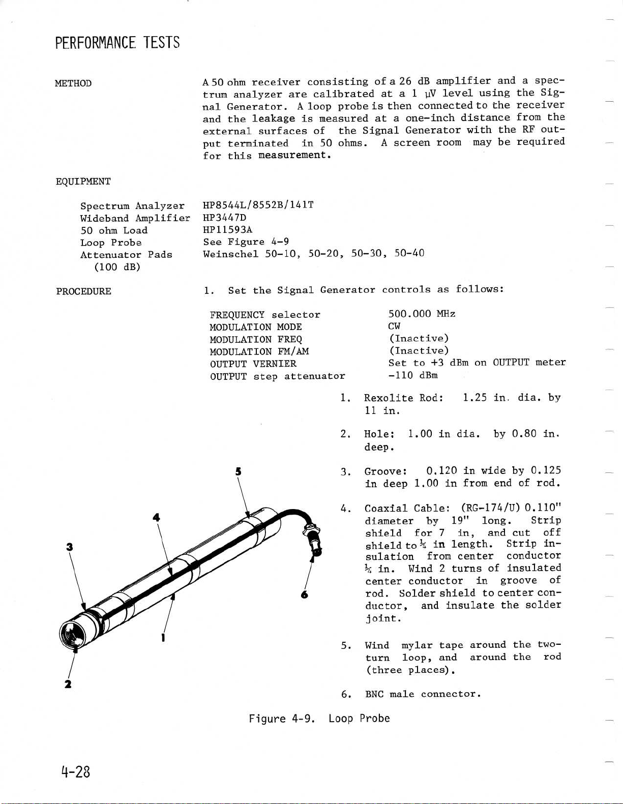
PERFORMANCE
METHOD
EQUIPMENT
Spectrum
WidebandAmplifier
50
ohm
LoopProbe
Attenuator
(100
PROCEDURE
Analyzer
Load
dB)
TESTS
Pads
A
50
ohm
receiver
trum
analyzer
nal
Generator
and the
externalsurfaces
put
for
HP8544L/8552B/141T
HP3447D
HP11593A
See
Weinschel
1.Set the
FREQUENCYselector
MODULATION
MODULATION
MODULATION
OUTPUT
OUTPUT
leakage
terminated
this
Figure
VERNIER
step
are
.Aloop
measurement
4-9
50-10,
Signal
MODE
FREQ
FM/AM
attenuator
consisting
calibrated
probe
is
measured
of
in 50
.
50-20,
Generator
the
ohms
is
Signal
.
50-30,
ofa26 dB
at
a
1
then
connected
a
one-inch
at
Generatorwith
A
screen
50-40
controls
500
.000
CW
(Inactive)
(Inactive)
Set
to
-110dBm
amplifier
pV
level
room
as
MHz
+3 dBm
using
to
distance
may
follows
on
and
a
spec-
the
Sig-
receiver
the
from
the
RF
the
be
:
OUTPUTmeter
out-
required
1
.
Rexolite
11
in
.
2.Hole
.
3
4
.
5.Wind mylar
:1.00
deep
.
Groove
in
Coaxial
diameterby
shield
shield
sulation
center
rod
ductor,
joint
turn
(three
:
deep
to
in
.
.Solder
.
loop,
1
Cable
for
Wind
conductor
places)
Rod
.00
1
and
0
.120
in
from
in
7
tape
and
:1
dia
in.wide
from
in
:
(RG-174/U)
19"
in,
length
center
2
turns
shield
insulate
.
.25
in.dia.b
.
by0.80
end
long
and cut
.Strip
of
in
to
around
around
by0.125
of
.
conductor
insulated
groove
center
the
the
the rod
in
rod
0
.110"
Strip
off
in-
con-
solder
two-
y
.
.
of
Figure 4-9
.
6.BNC
Loop
Probe
male
connector
.
Page 69

2.Connect
Model
3000
Signal
Generator
PFRFORMANCF
the
equipment
RF
Out
Figure
4-10
as
26 dB RF
.
shown
Amplifier
Input
RF
00
Step
Leakage
in
Output
4
Figure
Setup
4-10
.
Spectrum
TESTS
Analyzer
RF
Input
3.Set the
scan
width
the
input
to
-50
dBm
nal
in
the
brate
the
graticule
spectrumanalyzer bandwidth
to
0.5
attenuation
witha
10
display
analyzer
MHz/div,
to
dB/divvertical
using
for
the
the
the
0 dB and
center
-107
usingthelog reference
video
frequency
dBm
controls
4.Disconnectthe RF amplifierfrom
and
connect
RF
out
connector
attenuatorin
5.Set the
dBm,
and the
meter
6
Move
tor
signal
the
.
.Connect
the
with
(step
2)
PTR
loop
the
plus
.Recordthemaximum
.
a
OUTPUTVERNIER
the
noiseshouldbe
dB
100
of
a
50 ohmload
Signal
loop
probeover
two-turn
attenuatorpad
the
Signal
Generator
.
GeneratorOUTPUT
toa+3 dBm
.probetothe
the
loop
input
surfaces
at
less than
reading
a
to
100
filter
the log
scale
.
to
reference
Center
control
at
signal
the -31
.
the
SignalGenerator,
(10+20+30+40)
.
Terminate
step
attenuator
reading
of
of
the
the
on
RF
Signal
one-inchdistance
the
-107
dBmreference
in
dBmon
kHz,
100
level
the
.
Cali-
to
to
OUTPUT
the
amplifier
Genera-
.
line
46 of
the
Hz,
sig-
dBm
the
the
-10
.
The
Page 70

PERFORMANCE
MODEL
SEC
4 .2
4 .3
4 .4
4 .5
.1
4 .5 .2
4 .5 .3
4
.6
4
.7
4
.8
4
.9
4
.10
.11
4
.12
4
4
.13
4
.14
4
.15
4
.16
4
.17
4
.18
3000
FREQ
RANGE
FREQ
ACCURACY
FREQ
STABILITY
METER
ACCURACY
FLATNESS
STEP
ATT
HARMONICS
NON-HARMONICS
RESIDUAL
RESIDUAL
INT
MOD
CONTROL
FM/AM
AM
SYSTEM
AM
BANDWIDTH
AM
DISTORTION
FM
DEVIATION
BANDWIDTH
FM
FM
DISTORTION
IMPEDANCE
RFI
TEST
ACCURACY
AM
FM
FREQUENCY
ACCURACY
ACC
ACC
TEST
MINIMUM
39,999
1,454
RECORD
SPECIFICATION
.60
994
.99
.99
-0.5dB
-0
.75
-0
.7
-1
.5
26dBdown
dB
down
30
60 dB
down
dB
down
65
55 dB
down
down
35 dB
65 dB
down
380
950
1
.300
4
.300
27.5%
84
.5 %
4
.749
464.9kHz
21dBdown
MEASUREMENT
( )
kHz
kHz
kHz
dB
dB
dB dB
Hz
Hz
VDC
VDC
kHz
CHECK
kHz
kHz
kHz
VDC
VDC
kHz
kHz
kHz
kHz
kHz
kHz
dBm
S/N
DATE
MAXIMUM
Hz
Hz
dB +0.5dB
dB
dB
dB
dB
dB
dB
dB
dB
dB
dB
dB
dB
dB
dB
dB
dB
dB
Hz
Hz
Hz
% 32 .5 %
%
dB
dB
%
dB
40,000
1,015
1,545
SPECIFICATION
.40
.01
.01
104
500
+0
.75
+0.7dB
+1.5dB
200
420
1050
1
.700
4
.700
95
.5 %
3
3
5
.251
5
535
.1
-107
kHz
kHz
kHz
Hz
Hz 6
dB
Hz
Hz
Hz
VDC
VDC
dB 33
%
%
kHz
kHz
1
dB 42
4
%
2
%
dBm
LINE
1
2
3
4
5
7
8
9
10
11
12
13
14
15
16
17
18
19
20
21
22
23
24
25
26
27
28
29
30
31
32
34
35
36
37
38
39
40
41
43
44
45
46
Page 71

5
.1
INTRODUCTION
This
disassembling,
shooting
Measurements
facilitated
its
to
ments
5
5
sectionprovides
the
right
top and
and
.2
SERVICE
.2 .1
Disassembly
Model
and
by
side,
bottom
test
INFORMATION
calibrating
Signal
3000
adjustments
placing
as
access
of
points
.
Information
information
and
Generator
instrument
is
unit
for
trouble-
will
required
adjust-
for
be
on
SECTION
S
MAINTENANCE
by
removing
side
panel
.
the six
to
the
screws
instrument
(E)
.
holding
Refer
form part
bottom
should
side
be
One
strument
sembly
REMOVAL
rear feet
slight
by
REMOVAL
screw
with
cover
REMOVAL
may
the
removed
and
REMOVAL
can
to
panel
removed
side
reversing
a
by
be
meter
lifting
be
Figure
of
covers;therefore,
be
removed
.The
as
panel
to
to
the
OF
(A)
rear
OF
TOP
(B)
from
slight
reversing
OF
FRONT
removed
board
by
OF
SIDE
removed
5-1
.The
the
support
before
covers
indicated
must
remain
secure
chassis
BOTTOMCOVER
and
movement
COVER
rear
removing
rail
PANEL
to
the
.
lift
.Reinstall
the
removal procedure
-
top
and
movement
the
removal
TOP
RAIL
to
facilitate
assembly
upward
-
providebetter
Remove
side
for
the top and
these
removing
and
panels
below
front-panel
-
cover
lift
-
.
threescrews
.
Either
.NOTE
on
Remove
off
the
off
.
Reinstall
procedure
The
removal
The
side
top
panels
covers
either
can
the in-
as-
two
with
cover
single
cover
rail
rail
(D)
panel
access
of
is
:
Figure
5
.2 .2
a
.
.
REMOVAL
moved
to
down
slightly
module
REINSTALLINGMODULE
the
straight
carefully
chassis
down
connectionbetweenmodule
and
of
shown
by
top
screw
module,
screw
replace
module
in
Module
OF
of
while
from
socket,
.Module-cable
Figure
5-1
.
Servicing
MODULE
removing
the
(C)
chassis
and
seat
(C)
any
-
Modules
any
module
from
bottom
lifting
socket
-
check
properly aligned
module
to
cables
5-6
that
replace
insure
.NOTE
Disassembly
may
cables
and
removing
.
upward
.
Beforeinstalling
module
pins
module
a
and
attached
connections
:If
Rock
good
be
attached
hold-
module
to
pins
;
into
hold-
ground
chassis,
to
a
module
re-
free
are
then,
the
top
are
Page 72

MAINTENANCE
is
replaced
be
necessary
locked
See
CalibrationProcedure
tion
.
MODULE-PIN
pins
are
The
off-centerindex
module's
also
provides
#1
.
NOTE
in
each
used
are
system
INDEXSTUD
(off
center)
Figure
5
.2 .3
PRINTED-CIRCUIT
reinstalling
printed-circuit
is
properly
nector
proper
CAUTION
the
connector
modules
SIDE
VIEW
Figure
METER-BOARD
the
meter-board
the
attenuator
potentiometerretaining
with
to
loop
or
other
NUMBERING
numbered
being
:
module
All
plugged
a
method
16pins
;
installed,
remains
5-2
.
the
BOTTOM
Module
Printed-Circuit
BOARDCONNECTORS
a
board,
aligned
pins
and
direction
:
Failure
can
or
power
CABLE
CONNECTOR
PCB
CONNECTOR
5-3
.
(C315)
dial,
a
new
module,
calibrate
circuits
the
involved
in this
as
SYSTEM
shown
stud
in
for
-The
Figure
in
prevents
backward
locating
arenot
only
the
pins
butthe
same
VIEW
Pin
cable
be
with
that
(See
to
properly
result
supply
Connector
REMOVAL
.
Numbering
Board
connector
connector
.
_
END
Servicing
sure
the
board
Figure
in
J
VIEW
Alignment
-
Removal
numbering
connector
orientate
damage
assemblyrequires
VERNIER
nutand
it
will
phase-
sec-
module
5-2
required
actually
PIN
System
-
When
on
con-
faces
5-3)
RETAINING
CL
IP
that
knob
front
the
and
pin
SOCKET
of
and
to
top
rail
be
removed
secured
.
one
uator
of
screws
from
.
on
switch
thenbe
VERNIER
LEDand
panel
from
The
versing
When
care
MODULATION
to
through
dial)
meter
and
meter
wire
.
potentiometer
;
then
instrument
meter
the
installing
not
frontpanel
front
and one
board
disengagesix-pinconnector
board
connectors
The
moved
meter
the
board
removal
to
damage
BOARD
modulation-boardassembly
moved
engage
six
black
LATIONMODE
retaining
connector
a
from
screw
board
moved
.
clear
may
The
reversing
When
switches,
correct
of
switches
POWER
Supply
by
the
ment
connecting
carefully
by
the
following
the
slip-on
BCD
FREQUENCY
spring-loaded
and
nut
;
disengage
modulation
at
each
.The
board
toward
the
frontpanel;then,
be
lifted
board
assembly
the
placing
connectors
be
sureeach
switch,
main
harness
appear
SUPPLY
board
removing
BOARD
and
the
printedcircuit
rear
panel
harnesses,
lifted
.The
panel
.Remove
Remove
.
meterboard
by
three
(behindatten-
at
each
these three
three
from
meter-board
toward
assemblycan
rear
shaft,
board
clear
can
case
.
is
reinstalled
procedure
the
meter
the
UNLEVELED
(C316)
REMOVAL
can
procedure
connectors
from
switches
knobs
FREQ
EXT
;
from
switches
modulation
nine-pin
board
top
corner
;
and
of
assembly
rear
from
until
instrument
is
switch
reinstalled
removalprocedure
on
connector
switchcables
in
same
order
.
heatsink
four
.
from
REMOVAL
screws
board
After
the
the
-
can
which
to
removal
board
instrument
screws
top
attenuator
until
UNLEVELED
the
be
.
board,
-The
be
from
remove
the
;
connector
remove
modulation
can
then
the
assembly
.
.
FREQUENCY
break
The
be
removed
the
instru-
corner
slip-
front
lifted
by
NOTE
Lamp
:
MODU-
remove
levers
NOTE
is
Power
secure
of
can
the
re-
use
re-
Dis-
the
the
BNC
one
out
that
the
.
is
-
.
:
.
be
by
:
on
be
Page 73

The
Power Supply
raised
of
many
harnesses
power
instrument
must
CAUTION
far
enough
components
sti11connected
NOT
unless
be
to
board
allow
with
applied
the
may
checking
;
however,
to
negative
be
the
the
(ground)
to
the
and
of
C9
Power Supplyboard
The
by reversing
instrument
to
the
(jumper
side
of
positive
wires
the
removal
C10
chassis
(ground)
are
MAINTENANCE
is
connected
ground,
sufficient)
reinstalled
is
procedure
side
.
INSTRUMENT
Digital
Oscilloscope
Power
FrequencyCounter
Spectrum
5.3
Remove
bottom
cover
by reference
screw
off
.
before
In
general,
formed
Figures
and
measurements
chassis
.1
5.3
Connectdigital
volt
+18V
+18
.00V.(See
Voltmeter
Meter
Analyzer
CALIBRATION
the
cover,
.
The
from
top
Allow
calibrating
in
the
5-4,
adjustment
ground
+18VoltAdjustment
line
on pin3of
ADJ
.
PROCEDURE
instrument
and the
M172
module
to
Figure
of
module
a
two-hour
.
calibration
sequence
5-5 and 5-6
locations
are
madewith
.
voltmeter
on power
Figures
TABLE
module
supply
5-1
top
cover,
M172
can
5-6;then
and
slidecover
warmup period
should
given
.
for
.
reference
to
M30
5-5
.
RECOMMENDED
Accuracy
AC
dBm
to
the
per-
to
point
All
to
+18
5-6)
REQUIREMENT
50
.
CRITICAL
.04%
DC
and
At
least
Highfrequency
10
MHz
10-520MHz
-10
module
located
be
remove
be
Refer
test
NOTE
:
orange
and set
produce
to
and
TEST
coupled
mV/cmsensitivity
FrequencyRange
+15 dBm
5
Connect
volt
-18V ADJ
5.3.3
Connect
volt
readingmust
5.3 .4
Connectfrequency
input
Set the
switches
within
500
as
AM/FM
+10 dBm
- at
.3 .2
follows
EQUIPMENT
least
Power
-18
line
+7
line
Crystal-Frequency
ModuleM30
to
.000
MHz
Vernier
Range Model
Volt
digital
on
pin4of
on
power
.3
VoltCheck
digital
on
the
signal
to
the
:MODE
and
voltmeter
pin
be
+7
Model
a
high
counter's
.Set
at
VERNIER
RECOMMENDED
Keithley
Tektronix
HP
Model
Sensor
HP Model
Model
HP
Adjustment
voltmeter
moduleM30
supply
2
of
module
V
.3
counter
3000
RF
generator
frequency
front
to
CW,
minimum,
Maximum
8481A
to
for -18
to
±100
Adjustment
having
OUT
range
panel
FREQ
OUTPUT
179
5400
with
435A
Power
5303B
8558B
yellow
and
green
M30
.
mV
.
connector
FREQUENCY
which
s
such
controls
to
dial
clockwise
-18
set
.00h.
+7
.3
The
ohm
50
is
as
EXT,
at
.
.
5-
3
Page 74

MAINTENANCE
Adjust
ure
5-5)
on
counter
QUENCYADJUST
counterindicates
ed by FREQUENCY
counter
frequency
paragraph
5
.3.5
No
adjustment
5
.3.6
See
Figure
points
controls
and
other
Section
meter
justboth
producea
This
and+3
MHz,and
still
Set frequency
nect
to
M32A
for
a0V
queney
control
indication
FREQUENCY
M30
for
minimum
;
then,
from
RF
check
5.3
.11
PHASE-LOCKED
M31A
of
PHASE-LOCKED
M32A
5-5 for
and
Figure
.
Set
front-panel
5.3.4
to
voltageshouldbe
.0
note
within
scope
pin
to
(B)
M32A
M30
minimum
VDC
.
vertical
15.Adjust
scope
239
to
.
.Connect
pin
that
above
.000 MHz,
ADJUST
frequency
carefully
trimmer
the
switches
OUT
connector
will be
.
LOOP
module
LOOP
location
5-6 for
frequency
14,
-1
trimmers
reading
Set
frequency
voltmeterreading
limits
to
200
indication
againproducea
trimmer
clockwiseuntil
frequency
.
#1
M31A
is
#2
to
controls
digital volt
and
input
carefully
on
between
.
.000
MHz and con-
(DC,
M32A
.
and
(Figindication
turn FRE-
select-
Disconnect
.
A
final
covered
ADJUSTMENT
necessary
ADJUSTMENT
of
M32A
adjustment
200
.000
as in
(A
and
voltmeter
+0
to
.
239
1
V/cm)
control
Set
adjust
0
V scope
test
MHz
ad-
B)
.5
.000
(A)
FreM32A
in
is
to
5.3
.7
Phase-LockedLoop
P
.L .L.#3
M33
and the
moduleM33
justment controls
(Figure
and
Section
input
M9W
control
tion
.
.
.
V
Set
MODE
Vernier
input
Adjust
indication
FREQ
Set
presentation
5
.3 .8
Calibration
modules
points
M34
(Figure
trols
M9W
(Figures
Set
FREQUENCY
and
other
Section
meter
250
MHz
V
reading
maynowbe
Connectfrequencycounter
nector
(DC,
control
should
er
MHz
.
harmonics
on
to
adjust
multiples
If
this
readjust
break
to
multiple
obtained
consists
W
.
M9
(Figure
5-6)
.
Set
other
(DC,1
front-panel
to
(on
M9W
Phase-LockedLoop
are
are
to
and
1
V/cm)
NOTE
front
5
.3.4
(D)
FMx100,
at
maximum
M33 pin
control
of
to
400
of
:
M172,
located
5-5),
located
front
5
.3.4
M172
control
on
disconnected
connect
(A)
for
indicate
:Due
M9W
of 40
happens,
M9W
lock
of
witha250
panel
.Connect
V/cm)
for
controls
FREQ
5)
1
kHz
Hz
is
a
P.L.L.
M9W
while
5-4 and
switches
panel
.Connectdigital
pin
°).;then,
(Figure
voltmeter
to
M34
0Von
to
of
40
control
MHz
it
control
and
40
MHz
of
The
5-5),
FREQUENCY
to
.
(C)
and
on
scope
the
offset
will
MHz
#3
Adjustment
two
modules
test
point
while
are
on
controls
scope
M33 pin5.Adjust
a 0
V
scope
as
to1kHz
Set
scope
for AC,
for
minimum
sine
wave
note
400
#4
and
on
modules-
modulesM172and
5-6)
for 250
.The
pin8.Adjust
scope
a
frequency
MHz,
(A)
relock
until
that
Hz
sine
#4
Adjustment
involves
the
adjustment
.
controls
5-4)
.
to RF
vertical
.The
way
the
it is
(A)
for
from
be
necessary
several
"0
counter
the
module
to
250
vertical
indica-
follows
and
vertical
50
on
M34
.
M2Mand
.000
adj
ust
for
voltmeter
OUT
of
M34
possible
"0
250
at
the
V"
can
reading
:
is
as in
AM/FM
mV/cm
(null)
scope
scope
wave
three
as in
volt
a 0
input
count-
locks
V"
turns
The
ad-
M9W
MHz,
Test
con-
MHz
M172
.00
con-
M9W
250
MHz
next
on
:
.
.
.
at
.
to
be
.
Page 75

.
i
'>
-4
.
MAINTENANCE
U
1
6
,
2Z
rSJ~1
.
v
,1~,.~. .
VJ
C
o.d
~4214~J1
.
,A.
0,00
-0,q
,v
S
,)
),a()
G'+'v
t
airn
\
~
1
0
0
0000
3a
o
r
O
0
000
°
8
00000
1st
_2
h
.0
Set
FREQUENCY
adjust
M172
andacounter
this
step,
for
frequencies
Refer
tions
Set
just
ing
520
adjust
cations
to
Figure
.
FREQUENCY
M172
near
MHz
and
500
at
symmetrical
and
adjust
Set
100
.
Recheck
MHz
pot.asindicated
FREQUENCY
MHz.pot
scope
500
switches
300MHzpot.for
reading
using
applicableM172
of
350,
5-4
switches
500
MHz
pot
0V.
note
MHz
500
about
pot.t o
and 520
450
Increase
scope
0
MHz
500 and 520
to
100
.for
0
for 300 MHz and
OV
of
300
MHz
400 and
for
M172
to
500
for
a
.
scoperead-
FREQUENCY
indication
give
scope
MHz
V
.
Recheck
pot
.for
MHz;adjust
above
MHz
and
adjust
V
on
scope
Figure
on
.
450
pot
MHz
that
.
scope
Repeat
pots
MHz
loca-
.
.
Ad-
;
then,
indi
are
450MHz
0
V on
M172
and
5-4
.,
to
a
ioa
5~
~
G
.~',m~r1
.
M172
Controls
counter reading
using
and
is
.
MHz
Connect
Step
to
quencyhaving
then
VDC
5
0
obtained
.
520
at
.3.9
appropriate
MHz
.
Repeat
on
scope
digitalvoltmeter
through
MHz
frequencyrangefrom
in 10
highestleveler
adjust
this
AM/FM
M9W
frequency
Vernier
:1
of
100
MHz
M172 pots
.,for
this step
at
100,
to
MHz
steps
control
to
(B)
setting
VoltageAdjustment
.Repeat
50
until
50
M34
pin
find fre-
voltage
for
.
and
1
+1
MHz
0
14
MHz
V
0
.
;
.0
C316
The
NOTE
;
contains
ANCEADJ
adjustments
these
two
a
SIZE
pot
.
.
controls
Modulation
ADJ
pot.(C)
(D)
which
DO
NOT
.
change
Board
are
(C316)
and
a
factory
setting
BAL-
of
Page 76

MAINTENANCE
Connectdigital
MODT.P
AM/FM
to
adjust
+5
Vernier
indicate
5.3.10
To
rest on
erating
power
zero
adjust
bisect
Restore
to
Set
adjust
needle
meter
of
pletely
(A)
Set
FREQUENCY switches
to
dial
and its
powermeter
connect
connector
Adjust
dBm
panel
PUTmeter
dBm
for
set
turn
peat this
+3
without
pots.(E)
.Set
Verniercontrol
Figure
.00
adjust
stabilize
front
Meter
for
CW,
power meter
range
+3 dBm
power
dBm
5-6
modulation
Vreading
to
0
Meter Board
its
position)
to
instrument
OUTPUT
screw
dot
power
panel
Meter
again
scale
Board
cw
a
+3
front
VERNIER
to
+10
thermistor
thermistor
of
Meter
VERNIER
and
.
meter
front
powermeter
further
and
voltmeter
FREQ
for
on
0%
AM
V
±20
OUTPUTmeter,
bottom
meter
.
The
at
left
to
.
VERNIER
Board
bisects
.See
pots
and
adjust
dBm
panel
completely
dBm
.
the
to
Model
Board
for
set
Adjust
powermeter
to
panel
paragraphuntil+13 dBm
adjustment
(F)
tochassis
switch
control location
board
voltmeter
;
the
mV
.
Calibration
surface (normal
.
Momentarily
with
meter
end
instrument
pot.(B)
Figure
.
OUTPUTmeter
controls
to
Calibrate
or
+15 dBm range;then
or
3000
pot.(F)
reading
-7
dBmreading
power
Meter
the +15 dBm
VERNIER
readingsare
.
to
to
maximum
pot
voltmeter
the
and
front-panel
needle
of
meter
fully
at
dot
5-6
Set
Meter
50.000
cw
power
sensor
.
.
meter
Board
reading
fully
of
VERNIER
.
.Set
mechanically
and allow
untilmeter
left
for
VERNIER
Board
as
and
power
sensor
for
Set
MeterBoard
and
.Refer
and
(A)
for
AM/FM
should
C315
-
unit must
op-
turn
OFF
zero
should
scale
ccw;then,
end
location
com-
pot
reading
follows
MHz,
MODE
OUTPUT
meter
.
Set
to
RF
OUT
a
+13
front
OUT-
on
to
the
pot.(E)
.Again
range
and
cw
.
Reand
obtained
it
of
+5
Set
OUTPUT
to
the
pletely
for
a
+3
a
.
.
.
:
VERNIER
meter
range
-6
paragraph
meter
ther
and
Set
follows
MHz,
Vernier
to
range
Meter Board
Connect
not
within
.
dBm
adjustment
(D)
Model
MODE
dBm
0
for
a
Set
power
adjust
on
power
5
.3.11
erator
specified
quency
agree
carefully
trimmer
frequency
5.3
.12
See
Figure
justments
frontpanel
other
FREQUENCY
to
FREQ
mum,
+10dBm
at
shown
dial
to 0
+5
dBm
range
cw,
adjust
dBm
power
for
and set
AdjustMeter
powermeter
readings
.
:
control
.
and adjust
-3
AM/FMVernier
meter
Final
frequencycounter
and set
reading
accuracy
(See
FM Reference
.
front
VERNIER,
VERNIER
frequencycounter
on
dBm
-6
powermeter
until
3000
FREQUENCY
to
dBm
meter
in
is
to
.Record
+3
are
of
front
AM,
FREQ
to OI
Set
power
reading
to
pot.(G)
.
FrequencyCheck
front panel
Section
on
with
adjust
the
specifications,
M30 FREQUENCYADJUST
Figure
obtained
5-6 for
Connect
RF OUT
panel
40.000
AM/FMVernier
fully
dBm and
With
.
Meter
meterreading
reading
Board
reading
dBm
obtained
Meter Board
panel
switches
to
AM
meter
front panel
the
to 1001
for
5
.3 .4
counter
selected
5-5)
.
Adjustment
location
frequency
connector
controls
MHz,
cw
the
powermeter
VERNIER
Board
to
pot.(D)
.
Repeat
and
-6
without
controls
VERNIER,
and
OUTPUT
to
on
power
dBm
+5
AM
+3
dBm
to
signal
controls
.
;
until
of
;
as
MODE
OUTPUT
and
CW frequency
.
pot.(C)
.
on
OUTPUT
the
-5
dBm
power
pots.(C)
to
520
AM/FM
the
0
VERNIER
meter
range
.
Adjust
reading
-
M30
Note
if
it
FREQUENCY
desired
-
M29-1
M29-1
counter
then
follows
to
at
mini-
comTurn
dBm
for
this
fur-
as
.000
dial
dBm
.
and
gen-
as
fre-
does
very
ad-
to
set
:
CW,
dial
5-6
1(P/
V
~~
Clkt~1
Page 77

MAINTENANCE
Set
MODE
(B)
is
frequency
maximum
trol
reading
Set
MODE
maximum
frequencycounter
±10 kHz
5 .4
Troubleshooting
atic
A
thoroughunderstanding
diagrams
in
Section
the
a
particular
this
or
board
with
In
general,
the
module
The
with
indicator"lamps
phase-locked
in
each
which
is
unlocked
which
module
A
problem
many
and should
does
problem
for
example, will
lamp
supply
+18,
the
DPS2
rear
mance
the
CALIBRATIONPROCEDURE
For
troubleshooting
missible
to
FMxl_
to
produce
approximately
Increase
.
and
adjust
(B)
to
increase
by
5
kHz
to
FMx100
.
Adjust
.
TROUBLESHOOTING
procedure
and-circuit
3
of this
trouble
has been
the aid
front-panel
the
lights
loops
is
symptoms
not
.
to
flash
willextinguish
-18
panel
of
symptom
module
can
be
of
it is
or
PC-board
four
loop
loop
contains
to
.
are
at
fault
in
a power
be
clearly
The
loss
;
+7
and
power supply
of
the
these
to
operate
and
adjust
an
output
100
Hz
AM/FM Vernier
Modulation
frequencycounter
.
and
AM/FMVernier
M29-1
reading
is
generally
of
"divide
description
manualwill
to
PC
or
accomplished
replaced,
the
proper
preferable
assembly
ACCURACY
internal
aid
in
problems
an
indicate
The
lamps
unlocked,
.
supply
pointing
checked
while
.3
supplies
when
indicate
of
the -18
cause
loss
all
V
supplies
which
instrument
purposes,
the
M29-1
frequency
above
control
of
and
of
be
board
lamps
module
troubleshooting
.
indicatorlamp
when
indicate
but not
to
other areas
the
of
is
indicated
.
Model
control
the
Board
(A)_°or a
40
.500
a
system-
conquer"
the
block
located
enable
localized
.
the
module
or
repaired
schematic
to
replace
.
together
"unlock
Onemodule
that
which
may
cause
the
symptom
a
specific
V
supply,
ACCURACY
+18
the
lamps
.
comprise
forms
.Perfor-
it
is
3000
that
con-
MHz
Once
loop
only
The
the
per-
with
CW
to
to
to
in
any
of
the
plug-inmodules
removed;however,
be
turned
modules
available,
3000,
verifying
fective
RF
cables
module
meter
nected
for
powerlevel
Fabrication
cable,
.
.
V
for
connector
connection
Before
cedure,be
set
in
a
thorough
strument
loose
defectivemodule-pin
cables
5
.4 .1
The
following
cal
symptoms followed
cause(s)
It
is
properlycalibrated
a
warmupperiodwill
shooting
INTERMITTENT
ule-pin
LOWRF
is
10
rect
on
micro
actuated
LOWORNO RF
tive
attenuator
to
input
tive
meter
or
M9W
ule
MlOW
off
.
If
possibly
this
provides
if
a
.
can
output
or
spectrum
directly
of
terminated
modules
the
on
the other,
of
engaging
sure
proper
visual
for
or
missing
andburned
TroubleshootingHints
oratroubleshooting
assumed
.
OPERATION
sockets
OUTPUT
dB
lowon
the
switch
by attenuator
OUTPUT
or
output
board,
Checkvoltageonpin
.
.Thevoltage
the
when
removing
substitute
from
an
suspected
be disconnectedfrom
connectors
analyzer
to
the
or
frequency
a
short
in
a mating
one end and
on
test
equipment
inatroubleshooting
front-panel
operating
inspection
such
isalist
(+10
0
S1
obvious defects
screws,
sockets,
or
broken
the
instrument
previously,
precede
or
loose
dBm
RANGE)
this
rangebut
dBm
range,
is
probablynotbeing
(ANY
or RF
cables
of
attenuator,
defectivemoduleMIOW
or RF
instrument
or
installing
modules
another
easy
method
module
;
then
can
module
will
position
of
by
-
DefectivemodRF
shaft
RANGE)
should
connector
measurements
coax
connector
facilitate
.
controls
of
broken
loose
components
several
the
probable
procedure
has
trouble-
cables
If
-
Meter
.
-
connecting
15 of
be
cables
should
Model
is
a
power
be
con-
adapter
a
pro-
.
Make
the in-
wires,
typi-
been
and
that
.
power
is
cor-
Board
Defecdefec-
mod
approx-
are
of
de-
the
.
BNC
are
as
RF
.
.
5-7
Page 78

MAINTENANCE
imately
range
VbC
clockwise
proper
while
tive
on
power
is
attenuator
M10W
directly
should
If
is
Sweep
OUTPUT
is
trouble
driver
meter
movementmay be open
IC is
UNLEVELED
terminated
set
exceeds
defective
cables
Connect
output
for
50.000
from
powermeterreading
withUNLEVELED
operation
meter
repeat
is
tive
connection
put
lamp
defective
M10W
ACCURACYLAMPS FLASH CONTINUOUSLY
steady light
lights
as
follows:-2
withVERNIER
on
0
dBmrange
.
These voltages
operation
other
voltages,indicate
the
directly
correct,
output
this
defective
Oscillator
METER
pegged
remains
defective
so
.
.
a
+13 dBm readingon
MHz
10
directly
above
correct,
RF
is
is
.
values,
meter
at
be
approximately
level
at
is
IC
LAMP
in
that
+13
attenuator
power
Set
.Step
to
of
cable
correct
ON,
lamp-driver
in FM
board
at
the
or
its
is
low,
module
is
;
while
DOES
either
probablya defectivemeteron meterboard
at
.
ON
50-ohm
peak
dBm,
meter directly
OUTPUT
throughfrequency
520
MHz
lamp
moduleM10W
to
steps
trouble
or
at
RF
at
the
in
modes
.5
VDC
on +10
fully
of
1110W
trouble
RF
correct,
M9W
NOTMOVE
mechanical
of
defectivemodule
OFF
attenuator
.If
possiblya poor
OUT
MlOW
trouble
CW mode
clockwise
with
M9W
if
RF
in 10
of
indicate
VERNIER
the
particularly
a
.Next,
output
cables
measure
output
-10
the
is
defective
end
of
or
a
OUT
load,
modulated
or
connecting
dial
power
MHz-steps
+13 dBm
indicates
.Connect
attenuator
is
due
connector
but the
is
circuit
meter board
defective
.If
lies
.
If
RF
to
module M10W
level
-
If
scale, the
(C315)
zero,
meter-board
connector
AM
percentage
and
output
to
.
UNLEVELED
probably
in
but
a
defective
indicate
checkRF
-11
to
meter
a
flashing
dBm
;
-0
fully
posi-
in
the
module
level
-
this
dBm
is
low,
.
meter
.
meter
not
output
M10W,
M10W
VERNIER
range
.A
±0
.5
proper
power
and
output
defecground
If
out-
module
-
IC
it
If
RF
at
dB
.7
M29-1
flash
phase-locked
LOCKEDLOOPTROUBLESbelow
;
.
a
A
the
ment
normal
lock
PHASE-LOCKED
unlocked
module
of
tage,
phase-locked
or
ule
A
a
two
loss
willcause
M31
module
Failure
in
to
quencies
Table
levels
loops
or1V
frequency
are
zer
Table
values
represent
Phase-Locked
loop
M31,
M30
If
kHz signal
1
operating
between
signal
for
-18 V
or
M33
in
all modes,
normal
factors,
shorted
.
defective
chain-reaction
or
may
moduleM30
unlock,
bestmeasured
.
maybe
moduleM30
to
M31A
kHz
7.3V on pin
frequency
(in
the
for
phase-locked
causing
loop,
lamp,
lowDC-supply
RF cableora
more
of
.
NOTE
loops
the
PLL
not
M34,
of
the
sinceall
willbe lost
5-2
lists
for
Those
level
oscilloscope
:
5-2
is
only,
the
caused
M31
.
unlockindicator
as
signal
properly,
M30
is
beingapplied
on
pin
module
loops
vicinity
thelamps
LOOP
indicated
canbe
including
loop
RF cableormodulecan
to
1
kHz
#1
supply
causing PLL
MHz
40
will
typicalRF
each
signals
maybe measuredwithahigh-
TheTTL waveform
for
illustration
and
observedwaveshape
Loop#1
or RF
listed
is
correct,
and
of
8
If
.
is
TROUBLES
DC
effect
unlock
signal
to
cause
of
with
does
by a defectivemodule
M31A
6,
M31A,
ACCURACY
one
or
more
open
;
.
NOTE
range
voltages, improper
voltages,
unlock;thus,
a
-
thencheck
+18V on
of
the
of
560
MHz),
loop
to
flash
-
An
by
caused
:
proper
crystal
six
.
the
having
;
Unlocking
in Table
.
by
low
AC-input
defective
that
.For
to
moduleM31
#4 to
all
reference
signal-input
phase-locked
the
other
aspectrum
not necessarily
cable
is
on,
module
If
proper
to
M31A,
If
input
lamps
of
see
PHASE
:Above
instru-
it is
#4 to
.
open
a
lighted
a
number
an
causes
example,
module
signal
unlock
oscillator
four
loops
a
TTL
level
signals
analy-
shown
of
voltage
.
of
connecting
check
5-2
M30
RF
cable
1
check
pin
7,
signal
vol-
open
mod-
have
fre-
this
.
the
un-
or
to
.
in
1
If
is
kHz
and
5- 8
Page 79

MAINTENANCE
andDC
is
Phase-LockedLoop
#2
M172,
M30
Connect
and
stepping
200
voltmeter
per
239
operation
ModuleM30
the
at
Table
module
rect,
the
Phase-Locked
loop in
fective
nectingRF
ing
fective
TheM9W
the
directly
cified
operation
Measure
MHz
peroperation
the
Set
and
1.5to
is
nier)
level
properoperation
cated
voltages
defective
can be causedby
M30,
to
M32
observe
to
239
MHz
from
MHz
.
1
MHz and
the
5-2
M30
the
RF
cables
in
FM
moduleM29-1
1198
in
the
signals
signal
MODE
AM/FM
2.5
dependent
directly
is as
.
.
M32
.
digital
voltmeterreading
through
MHz
reading
0 V
Thesevoltages
of
moduleM172
can
M30
.
indicate
.If
trouble
Loop
CW
mode canbe
modules
cables
modes
can
be checked
MHz
at
module
Table
of
the
1200
directly
levels
switch
Vernierat
MHz
uponsetting
are
#2 -
or RF
voltmeter
frequency
in
1
should
at
200
be
checkedby
1440
MHz
The
levels
the
M30
lies
.
#3 -
M9W,
.
In
can
narrow
M9W
5-2
M9W
MHz
of
the
specified
to
FMxl,
signal
at
moduleM29-1
specified
of
module
correct,
Unlocking
defectivemodules
cables
MHz
MHz
signals
proper
outputs
in
Unlocking
M30,
addition,
be
.
oscillator
.
indicates
.
(120
at
module
M30
FREQ
maximum
(exact
in
module
connecting
to
M32
range from
steps
change-0
to -7
indicateproper
.
measuring
specified
operation
are
module
caused
M33
caused
by
The
is
of
M29-1
by a de-
measuring
level
comb)
M30.Pro-
indicated
in
Table
at
.
frequency
AM/FM
.
If
Table
is
M31A
of
loop
pin
while
.
The
.2
.8Vat
directly
cor-
M32
of this
by
de-
or
con-
unlock-
signal
spe-
proper
and
5-2
VERNIER
Measure
Ver-
signal
5-7
.
indi-
by
in
of
or
11
If
input
ules
trouble
ing
RF
Phase-Locked
may,
#4
caused
otherloops
3
should
troubleshooting
Unlocking
V
2
.
s
defective
M32,
Connect
The
voltmeter
withFREQUENCY
-2.5V
These
module
of
pin8.The
+6 to
and-8 V
are
obtained,
properly
Measure
moduleM9W
tween
upon
es
.If
in
Table
correctly
Measure
The
40
MHz
should
and the
Table
operation
Measure
at
moduleM32
dependent
FREQUENCY
specified
erating
Last,
output
signals
M9W,
M30
and
is
in
module
cables
by
M34
digitalvoltmeter
at
voltages
+7 V
.
the
1198
the
setting
the
the
MHz
levelshould
5-2
the
properly
measure
of
.
Loop
under
problems
.
Therefore,
be
operatingproperlybefore
loop
of
modules
or
connectingRF
250 MHzand
indicate
M22
.Connectvoltmeter
voltmeter
at
000
at
500 MHz
module
Wide
.
The frequencywillbe be-
MHz and
signallevel
5-2,
.
40
harmonics
be
fairly
.
This
of
the
1448
.
upon
switches
in
Table
the M31
to
module
M29-1
M33
#4
- Unlocking
certain
originatingin the
loop
#4
M172,
reading
switches
-5
MHz,
.
M172
Oscillator
1718 MHz,
of
the
module
comb line
from
equal
be
level
M30
module
MHz
to 1487
The
exact
the
setting
.
If
5-2,
.
the
10
module
M33
are
correct,
or
conditions,
loops#l,
#4
.
can
becaused
M9W,
cables
to
should
set
.0Vat
proper
reading
0Vat
If
these
is
FREQUENCY
is
as
M9W
is
at
40
in
as
specified
indicates
.
frequency
the
the
MHz
to9.001
.The
from
its
connect-
of loop
2
M30, M31,
.
M172
at
moduleM30
of
level
pin
be0.00
000
500
operation
to
shouldbe
250 MHz
voltages
operating
signal
depending
switch
specified
operating
MHz
to
amplitude
proper
MHz
signal
the MHz
is
M32
is
output
MHz,
MHz
mod-
the
be
:and
by
1 .
V
.
M2M
at
.
280
in
is
as
op-
MHz
5-9
Page 80
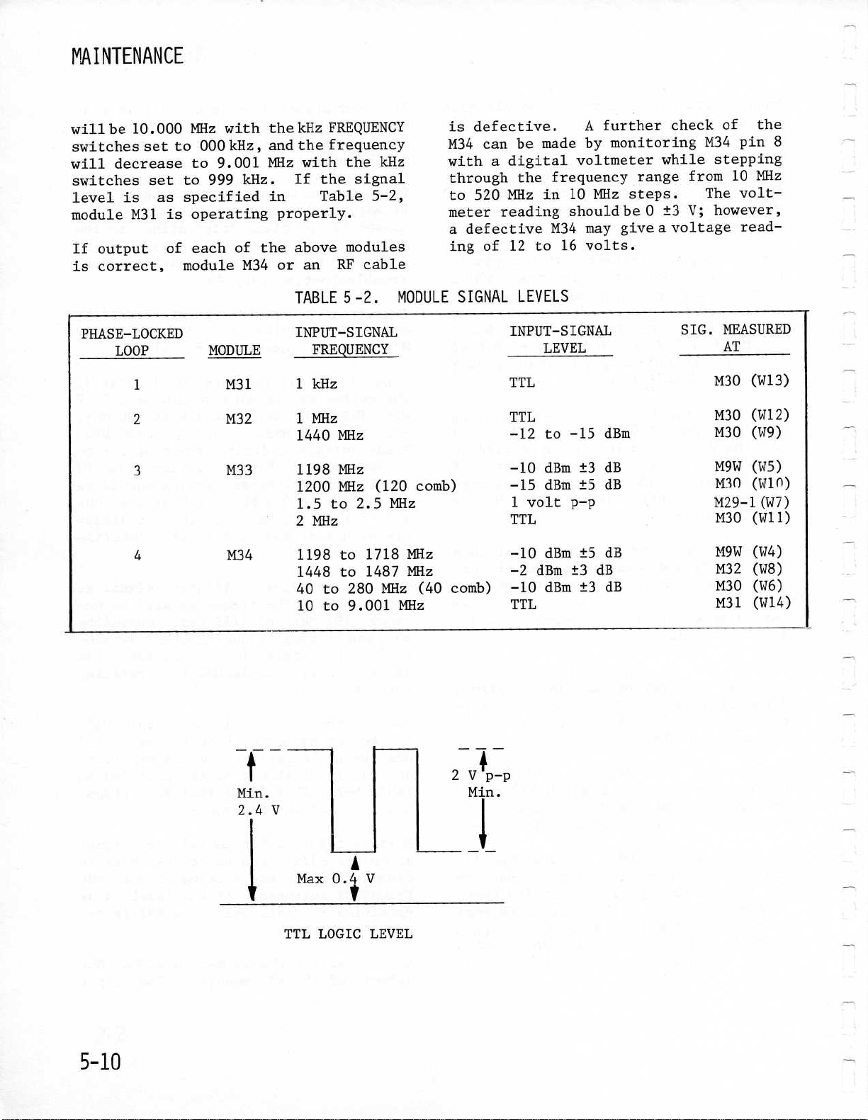
MAINTENANCE
Digitally signed by
http://www.aa4df.com
10
is
.000
set
set
as
M31
willbe
switches
willdecrease
switches
level
module
If
output
is
correct,
MHz
to
000
to9.001
to
999
specified
operating
is
each
of
moduleM34
with
kHz,
kHz
of
kHz
the
andthe
MHz
with
.
If
in
properly
theabovemodules
or
an RF
FREQUENCY
frequency
the
signal
the
Table
.
kHz
5-2,
cable
is
defective
M34
can
be
with
meterreading
through
to
520
a
defective
ing
of
a
digital
the
MHz
12 to 16
.A
made
frequency
in
M34
further
by monitoringM34
voltmeterwhile
MHz
10
should
may
volts
check
range
steps
be0t3V;
give
.
from
.The
avoltage
of
the
pin
stepping
MHz
10
volt-
however,
read-
8
PHASE-LOCKED
LOOP
1
2
3
4
MODULE
M31
M32
M33
M34
TABLE
INPUT-SIGNAL
1
1
1440
1198
1200
1.5to2.5
2
1198 to 1718
1448 to 1487
40 to
10
5-2
.
FREQUENCY
kHz
MHz
MHz -12
MHz
MHz
(120
MHz
280 MHz
to9.001
comb)
(40
SIGNAL
comb)
MODULE
-
MHz
MHz
MHz
MHz TTL
LEVELS
INPUT-SIGNAL
LEVEL
TTL
TTL
-15
to
dBm
-10
-15
1
TTL
-10
-2
-10
volt
dBm
dBm
dBm
dBm
±3
±5
p-p
±5
±3 dB
±3
SIG.MEASURED
AT
M30
M30
dBm M30
dB
dB
dB
dB
M9W
M30
M29-1(W7)
M30
M9W
M32
M30
M31
(W13)
(W12)
(W9)
(W5)
(Win)
(W11)
(W4)
(W8)
(W6)
(W14)
TTL
LOGIC
LEVEL
2 V
Min
P-P
.
Page 81

MAINTENANCE
BCDFREQUENCY
BCD
switch
defective
switch
Five
plus
from
uses
only
5
.
eachof
Table
Suspected
by
3000
module
frequency
frequency
grounded
100's
are
kHz
NOTE
MODULATIONTROUBLES
Board
of
when
Non-linearamplitude
higher-audio
nal
output
connector
of
.the
a
ground
0
through
three
needs
A
"BCD
the
5-3
referring
Wiring
pins
.
by selecting
MHz
grounded
switch
TABLE
Decimal
modulation
5-3
Digit
0
1
2
3
4
5
6
7
8
9 0 - - 0
:
0
(C316)is
the
source,
amplifier
SWITCHES
circuits
switch,
switches
to
9.The
wires
to
select
Truth
silk
.
switch
to
Table
Diagram
are
grounded
For
of
200
.500 MHz,
switch,
by
.
.
BCD
Wire
Wire
problems,
modulating
frequenciesfrom
may
be
.
-
Troubles
maybe
looseor disengaged
orabroken
utilize
select
100's
plus
Table",
switches,
problems
example,
digit
Groundedby
NOT
the
ground,
digits
5-3 and the
to
determine
and M31
5
FREQUENCYSWITCHES
Grounded
-
mostcommon
signal
caused
caused
switchwire
four
decimal
MHz
between
applicable
is
given
canbe
for
a
particular
to
M172
digit
BCD
8 4 2
-
-
- -
-
- 0 -
- 0 - 0
- 0 0
- 0 0 0
0
The
modulation,
2
pins
on
the
Wires
- - -
- - 0
0 -
-
0 0
-
-
- - -
Switch
.
Modulation
particularly
is
an
by the
in
wires
digits
switch
since
checked
Model
which
select
pin
on
2
and
100's
1
cause
lost
exter-
M10W
the
by
a
.
it
0
and
to
in
a
3
is
the
4
.
.
at
Thepresence
can
be
determined
switch
nier
nect
T.P
peak-to-peak
of
FREQ
should
frequency
Failure
signalsindicates
Board
Connect
M10Wpin
should
amplitude
Set
should
a
Failure
signals
defectiveMODEswitch
Board,
ulation
Connect
M29-1
or
a
of
scope
wave with
Failure
signals
switch,
Modulation
5.4 .2
While
work
ing
high accuracy
able,
lowed
circuits
and
The
replaced
recommended
to
to
oscilloscope
.The
400
Hz
switch
be
to
.
scope
be a
FREQ
display
p-p
value
to
at
orabroken
Board
scope
pin
FMx100
400
Hz
V
.
10
indication
to
maybe
or
Module
in
satisfactorily
a
defective
module
by calibration
.
theadjustmentsneeded
M172,
of
AM,
FREQ
100%
and
scope
sine
(period
to1kHz
a 10
of
15
of
switch
this
16,
.
sine
Set
a
Board
many
M9Wand
individually,
V p-p
1
kHz
obtain
vertical
.
The
1
kHz
approximately
a
400
of
obtain
point
and
vertical
and set
The
scope
wavehaving a
FREQ
an
amplitude
obtain
due
brokenwire
Replacement
cases
module,
of
which
replacement
Table
that
the
OUTPUT
a
to
approximately
should
and
5-4
thesethree
.
modulating
as
follows
to
400
Hz,
to
+3 dBm
vertical
should
wave
of2.5
sine
(period
the 400
defectiveModulation
scope
sine
400
Hz
the
on
wire
theMeter
MODEswitch
displayshouldbe
switch
the
to
moduleM29-1
the
aftersimply
of
lists
M10W
input
display
at
a
-
scopedisplay
wave
Hz
input
wave
-1.75
Hz
.The
sine
wave
400
Hz
maybe
the
between
Board
input
to1kHz
a1kHz
be
of
400
Hz
a
defective
between
Model
to
maintain
the
unit
should
the
each
.
modules
however,
signal
:
Set
AM/FM
.
to
a 10
frequency
ms)
.
at
of
1
or
to
module
indication
with
V p-p
having
1
.75V.
or
due
Modulation
the
.
to
module
to
p-p
.
10Vp-p
or
.
3000
replac-
is
be
affected
module
maybe
it is
modules
MODE
VerCon-
MOD
Set
ms)
1
kHz
scope
1
kHz
to a
Mod-
FMxl
value
The
sine
1
kHz
MODE
the
will
the
capfol-
.
V
a
.
an
.
.
be
5-
11
Page 82

MAINTENANCE
replaced
ment
of
it
is
recommended
replacedas
be
MODULE
REPLACED
M9W
Sweep
M10WOutput
M172
M29-1
M30
Crystal
M31 kHz
as
a matched
the
M30
or
a
Oscillator
Amplifier
Sweep
FM Reference
Drive/DAC
Reference
Steps
set
M32becomes
that
these
matched
TABLE
.
If
replace-
necessary,
two
modules
set
also
.
5-4
.REPLACEMENT
ADJUSTMENTREQUIRED
(See
appropriate
Reset
Recalibrate
Reset
ResetFM ReferenceAdjustments
Set
None
Phase-LockedLoops
Phase-Locked
Crystal-FrequencyAdjustment
required
MODULE
paragraphs
MeterBoard
(4,
Loop
tL
CALIBRATION
#3
(C315)
#4
',3
-~
in
and
'Sic
Calibration
#4
-
M29-1
and
Final
~a2
Procedure)
Freq.Check
M32MHz
M33
Narrow
M34Wide
C315
MeterBoard
C316
Modulation
DPS2
Power
Steps
Osc.Lock
Osc.Lock
Supply
Board
AdjustPhase-LockedLoop
Adjust
Set M34
AdjustMeter
Set
Adjust+18V
Phase-LockedLoop
Leveler
Board
AM/FMVernier
and check+7
Voltage
Calibration
Voltage,
#2
#3
(pin
.3
and
V
14)
for
Reference
FM
+1.0VDC
.SEE
Adj
PLL
#4
.
Page 83

MAINTENANCE
QFREQUENCY
02PLL
03
®PLL
2
PLL3T
4TP
Figure
TP
ADJUST
P
5-5
.
Test
Points,
Chassis
Qs
MODULATION
(s
©
MHz
250
LEVELER
WIRE
GREEN
ORANGE
YELLOW
(OTHERS
BottomView
TP
TP
COLOR
+7
T
P
CODE
.3V
+18V
-18V
UNASSIGNED)
5-
13
Page 84

Page 85

(1)
DPS2A
A-
+18VADJ
B--18
FUSE2AT
C
-
(2)
NOT
(3)
M37
(4)
NOT
(5)
NOT
VADJ
USED
AUX
USED
USED
POWER
RF
SUPPLY
OUT
(OPT
MAINTENANCE
4)
(6)
M30
A-1440MHZ
B-1440
C-10MHZTP
(7)
M34WIDE
A-RFTP
B-UNLOCK
(8)
M9W
A-WIDE
B-WIDEOSCLEVADJ
C
-NARROW
D
-NARROW
(9)
M10W-9
(10)
M31A
A-UNLOCK
M172
(11)
(12)
M32A
A-000
B-039
C-UNLOCK
(13)
M33
A-RFTP
B-UNLOCK
(14)
M29-2
A -
2.5MHZ
B-2
MHZ
XTAL
MHZ
SWEEP
OSC
OUTPUT
KHZ
SWEEP
MHZ
MHZ
MHZ
NARROW
FM
ADJ
REF
ADJ
ADJ
OSC
LOCK
INDICATOR
OSC
CENT
OSC
SW
OSCLEVADJ
STEPS
INDICATOR
DRIVE/DAC
STEPS
ADJ
ADJ
INDICATOR
OSC
INDICATOR
REF
ADJ
ADJ
AMP
ADJ
LOCK
II
(11)
(4)
i~
il
II
I
Oc
Ll
®B
(12)
II
OBE
II
(2)
(10)
©A
rU
0
(3)
I
3
®
_
c
3
(D
®e
®
-
i
~I
.~
I
/:Ds
(14)1(15)
.
,~.
1
.
p7)(18)
I
I
I
I
~~(A)
3
:3
'
BO
--
~~
~(9)
o0
5
.
(16)I
I
c
l
L
®~a
D
I
II II~III
M35-1RFCKT
(15)
(16)
50130-01
(17)
C316
A-
+5VADJ
B-FMx1
C-SIZE
D-BALADJ
(18)
C315
A-METER
B-METER
C-LEVEL0DBM
D-LEVEL0DBM
E-LEVEL
F-LEVEL
MOD
G
-%
STEP
MOD
ADJ
ADJ
METER
CAL
BAL
+10
+10
ADJ
BOARD
ADJ
ADJ
DBM
DBM
BKR
ATTEN
BD
RANGE
RANGE
RANGE
RANGE
(OPT
3)
3000
Figure
+3
ADJ
-7
ADJ
+3
ADJ
+13
ADJ
5-6
.
Model
Top View
Page 86

6.1
This
For
an
appears
The
lists
INTRODUCTION
section
assembly
first,
appear
contains
containingoneor more
and
lists
is
followedby
in
the
PARTS
1010-00-0013
1219-00-0016
1212-00-0006
1110-00-0294
1110-00-0751
1115-00-0011
1218-00-0250
1218-00-0144
of
following
LIST
all
the
order
replaceable
subassemblies,
subassembly
.
SECTION
REPLACEABLE
parts
for the
the
list
.
ASSEMBLY
3000
HARNESS
POWER
C315
C316
DPS2A
PC-DPS2A
LINE
SWITCH
CORD
assembly
-
3000
-
DPS2A
instrument
6
PARTS
.
list
1114-00-0020
1219-00-0055
1219-00-0054
1114-00-0360
1218-00-0600
1218-00-0610
1114-00-0016
1114-00-0012
1218-00-0192
1114-00-0143
1114-00-0215
1218-00-0022
1218-00-0021
1219-00-0117
1219-00-0118
1114-00-0011
1114-00-0008
1219-00-0129
1219-00-0019
1218-00-0314
1218-00-0334
1219-00-0020
1114-00-0320
M9W
MIXER
PREAMP
M10W-9
AMPLIFIER
LEVELER- MIOW-9
M29-2
M30
PC
M31A
M32A
DIG
OSC
MIXER
VIDEO
M33
M34
MIXER/AMPVIDEOAMP
LEVELER
PHASE
VIDEO
M172
-
PGM
CTL
-
M9W
-
M30
BD
BD
-
M32A
AMP
-
LOCK-
MIXER
M9W
-
M10W-9
- M32A
- M32A
- M32A
M34
-
M34
M34
M34
- M34
6.2
The
MANUFACTURERS
following
code
CODE
is
usedon
the
parts
lists
to
identify
the
manufacturer
.
Page 87

ABBRV
NAME.. .
. ... . . ...
. .
. .
. .
. .
. ...
.
.
CITY..
. .
. .
. . ... . .
. ...
ST
A-B
A-D
A-H
A-I
A-M
A-P
ASAC
ACEIN
ACI
AEG-T
AER AVX
AERTK
AHAM
AIN
ALC
ALLPL
AMD
AMELC
AMP
ANZAC
APL
APP A-P
APX
ARC
ARN
ARW-M
ASC
ASE
ASTIRASTRO
AT/IN
ATC
ATR ATR
AUGAT
AULT AULT
AUTCP
AVDELAVDEL
AVT
AWC
B-T
BEARIBEARINGS,
BEK
BEL
BER
BGH
BORDN
BOLE
BREZ
BSCAN
BUCK
BUD BUD
BURND
BUS
BWC
C-D
C-E
C-H CUTLER-HAMMER,
C-I
C-J
C-K
C-L
C
C-W C-W
CAI
CAM
CAR
CCM
CDC
CECO
CFI
CGW
CHE
CHEMP
CHLAR
CHOM
CHRY
CIMCO
ALLEN-BRADLEY
ANALOG
ARROW
ALANINDUSTRIES
AMERICAN
AMERICAN
ABACUSPACKAGING
ACE
ADVANCE
AEG-TELEFUREN
AERTECH
M
INDUSTRIAL
CERAMICS
AHAM
ALPHA
ALCO
ALL
ADVANCEDMICRO
AMERICAN
AMP,
ADAMS-RUSSELL,ANZAC
AMPHENOL
AMPEREX
ARCOELECTRIC
ARNOLD
ARROW-M
ASSOCIATED
AIRCOSPEER
ATLANTIC
AMERICAN
AUGAT, INC
AUTOMATION
AVANTEK,
ALPHA
BEK-TEK,
BECKMAN
BELDEN
BERG
BEECH
BORDEN
BOURNS, INC
BREEZE
B-SCAN,
BUCKEYE
BURNDYCORP
BUSSMAN
BARON
CORNELL
CLINTON
COMPONENTS,
TRW/CINCH
C & K
CENTRALAB
C-M
CUSTOM
CAMBION
CARLING
CORCOM,
COMPONENT
CENTRAL
CIRCUIT
CORNING
CHERRY
CHEMPLAST,INC
CHARLES
CHOMERICS
CHRYSLER
CIMCO
COMPANY
ELECTRONICS
PLASTICS,
INC
PRODUCTS
COILCO
INC
ELECTRONICS NEW
RADIO,
INDUSTRIES
DEVICES
HART,
COMPONENTS,
INDUSTRIES
INDUSTRIES,
.
ELECTRONIC
ENGINEERING
CORP
INDUSTRIES
.
FASTENER
WIRE
INSTRUMENTS,
CORP
GROVE
INC
CORPORATIONS,
INC
STAMPING
MFG
WIRE
DUBILIER
ELECTRONICS
COMPONENTS,
ACCESSORIES,
ELECTRIC,
INC
COILCO
FUNCTIONS
GLASS
ELECTRICALPRODUCTS
LARSON
WIRE
INC
.
MAGNETICS
PLASTICRAFT
HDWR
CORP
INC
ELECTRIC
CONNECTOR
INDIA
TECHNICAL
.
INC
INC
INC
.
DIV
DEVELOPMENT
INC
CORP
DEVICES
PRODUCTS SHELBYVILLE
.
SPRING
ELECTRONICS
RUBBER
.
CORP
.
SYS
.
.
.
.
HARDWARE
.
.
INC
.
.
.
AND
CABLE
INC
INC
.
.
.
.
WORKS
.
CO
.
.
AND
CABLE
CO
CO
.
.
INC
.
INC
.
PRODUCTS
.
CORDSETS
DIV
SYSTEMS
CORP
CO
.
CERAMICS
.
INC
INC
CO
.
CORP
ELECT
.
INC
.
INC
INC
.
INC
.
.
INC
MILWAUKEE
CAMBRIDGE
KETTERING
COLUMBUS
CARTERVILLE
.
.
INC
.
.
COMPANYCHICAGO
.
.
.
.
DIV
.
CORP
.
.
CHICAGO
CHICAGO
CAMDEN
CENTERBROOK
SOMERVILLE
MYRTLE
SUNNYVALE
AZUSA
NO`RTHNANDOVER
INDIANAPOLIS
SUNNYVALE
BENSENVILLE
HARRISBURG
BURLINGTON
BROADVIEW
PAINESVILLE
SLATERSVILLE
MARENGO
CARSON
BRISTOL
ST.MARYS
DAYTON OH
HUNTINGTON
BLOOMINGTON
ATTLEBORO
MINNEAPOLIS
PECKVILLE
PARSIPPANY
SANTACLARA
ELIZABETH
READING
CLEVELAND
FULLERTON
GENEVA
CUMBERLAND
BEECH
COLUMBUS
RIVERSIDE
UNION
PHILADELPHIA
COLUMBUS
WILLOUGHBY
NORWALK
ST.LOUIS
NILES
.
NEWARK
ROCKFORD
MILWAUKEE
BIDDEFORD
ELK
GROVE
WATERTOWN
MILWAUKEE
WARMINSTER
SKOKIE
CAMBRIDGE
WEST
CHICAGO
CARSON
BRAZIL
NEWBURY
CORNING
WAUKEGAN
WAYNE
STERLING
WOBURN
DETROIT
ALLENDALE
BEACH
GROVE
HARTFORD
PK
STATION
VILLAGE
WI
MA
OH
IN
IL
IL
IL
NJ
CT
NJ
SC
CA
CA
ME
IN
CA
IL
PA
MA
IL
OH
RI
IN
IL
CA
CT
PA
IL
NY
IN
MA
MN
PA
NJ
CA
NJ
PA
OH
CA
IL
PA
IN
OH
CA
NJ
PA
OH
OH
CT
MO
IL
NJ
IL
WI
ME
IL
MA
WI
PA
IL
MA
CT
IL
CA
IN
CA
NY
IL
NJ
IL
MA
MI
NJ
Page 88

ABBRVNAME
CKI
CLAR
CLFRM
CLFX
CNCRD
CPKG
CPLRD
CRTR
CTS
CTS-ECTS OF
CTS-F
CTS-KCTS OF
CTSBRCTS OF
CTSBVCTS OF
CW/AL
DAL
DATEL
DAV
DAYTN
DEL
DEN
DEW
DILEC
DIO
DK-WR
DLGHT
DNTCH
DRA DRAKE
DRMYR DORMEYER
DYNR DYNEERCORP
E-C
E-I
E-M
EBY
ECKDT ECKARDT
ECMC
ELC-I
ELCO ELCO INDUSTRIES
ELEXP ELECT
ELFX
ELHDW
ELNA ELNA
EMRON
EPITK EPITEK
EPOXT EPOXY
ETC
ETY
EVRDY
EXAR
EZLOK
F-K
F-S FEDERALSCREW
FAN
FASTX
FCD
FNWL FENWAL
FRK
FRTE
FRXC
G-E
G-H
G-I
G-T
GAL
GATESGATES
GBN
GCE
GHZ
GLOBE
GNATR
GOU
DRIESDRIES REPRODUCER
GRIP
GRVCO
GUDL GUDEBROD
GRAYHILL,
GEN'L INSTRUMENT
GRAND
GALILEO
GILBERTENGINEERING
GC
GHZ
GLOBE
GENERAL
GOULD,
GRIPMASTER
. . . . ... ... ... . . .
CTS
KNIGHTS,
CLAIREX
CLAROSTAT
COILFORM
COLE-FLEX
CONCORD
CREATIVEPACKAGING
COMPLETE
CORE-TRONICS ORANGE
CHICAGO
C
.T.S.OF
C.W./ALPHA
DALE
DATEL
HARRY
DAYTON
DELEVAN
DENNISON
DEWIREFABRICATING
DILECTRON
DIODES,
DAKO-WARE
DIALIGHT
DONTECH,
ELECTRONICCRYSTALS
ELECTRICAL
ELECTRA/MIDLAND
EBY
ELECTRI-CORD
ELECTRA
ELECTRO-FLEX
ELECTRONIC
ELECTRONICTRANSISTOR
ERIE
EVEREADY
EXAR
E-Z
THERMWELL
FANCOURT
FASTERDIV
FAIRCHILD MOUNTAIN
FRAKO
FAIR
FERROXCUBEDIVISION SAUGERTIES
GENERAL
ELECTRONICS
ROVE
CORP
.
MFG.C
CORP
FLEX NEW
READING
TELEPHONE
ELKHART
FAIRBERRY
KEENE
BERNE
BROWNSVILLE
TECHNOLOGY
SYSTEMS,
DAVIES
ELECTRICCO
DIV
.
MFG.CO
INC
.
INC
MANUFACTURING
COMPANY
EXPEDITERS MILWAUKEE
ELECTRONICS
TECHNOLOGY,
TECHNOLOGICAL
INTEGRATED
LOK
RITE
TRANSFORMERS
ENERGYPROD
DEVICES,
INC
COMPANY
.
.
INDUSTRIES,INC
LABORATORIES
HARD
PRODUCTS,
&
CO
.,
PRODUCTS
ELECTRIC
INC
ELECTRO-OPTICS
ATRONICS
.
CO
BROS.SILK
. .
. ... .
INC
.
O
.
DIV
.
SYSTEMS
CORP
INC
MOLDING
CORP
MFG.CO
HEAT
SYSTEMS
.
ILL.TOOL WORKS DES
.
INC
.
.
.
.
CO
.
.
CORP
CO
.
.
.
INC
INC
.
INC
.
CORP
PRODUCTS
INC
CORP
.
SEMICONDUCTOR
.
CO.INC
CORP
.
CO
.
. . .
CITY..
MT.V
DOVER
GENEVA
BABYLON
INDIANAPOLIS
CHICAGO
ELKHART
FAIRBERRY
PASO
BERNE
BROWNSVILLE
SOUTHAMPTON
HARTSDALE
.
.
.
.
.
.
MANSFIELD
CHICAGO
CHICAGO
EAST AURORA NY
FRAMINGHAM
LOWELL
MONROVIA
CHATSWORTH
CHICAGO
BROOKLYN
HARWOODHEIGHTS
ROCKVILLE
CHATSWORTH
KANSAS
MURRAY
MINERAL
PHILADELPHIA
ORANGE CA
WESTFIELD
CUMBERLAND
ROCKFORD
BLOOMFIELD
FARMINGDALE
CARSON
KANATA,
BILLERICA
FLUSHING
ERIE PA
NEW YORK NY
SUNNYVALE
GARDENIA
FRAMINGHAM
CHICAGO
GREENSBORO
FRAMINGHAM
FRANKFORT,
WALLKILL
INDIANAPOLIS
LA
HICKSVILLE
GRAND
CARMEL
DENVER
.
PHOENIX
ROCKFORD
CHELMSFORD
MILWAUKEE
PHILADELPHIA
ST.
NEW
MARLBORO
DAYTON
CHICAGO
. .
E
NON
YORK
ROBLES
CITY MO
HILL NJ
PLAINES
GRANGE
HAVEN
PAUL
ROCHELLE
;
. . ... .
WELLS
ONT
VIEW CA
.,
GER
. ... . .
CAN
.
.
.
ST
NYCLA
NH
IL
NY
NY
IN
NJ
IL
IN
IL
CA
IN
TX
PA
NY
MA
IL
IL
MA
MA
CA
CA
IL
NY
IL
IN
CA
TX
PA
PA
IN
IL
WI
CT
NY
CA
S
##
MA
NY
CA
CA
MA
IL
NC
IL
MA
NY
NY
IN
IL
NY
MI
IN
CO
AZ
IL
MA
WI
PA
MN
NY
NJ
OH
IL
Page 89

ABBRV
NAME
. . ...
. ...
. .
. ......... . ... .
CITY.. .
. .
. .
. ..... .
. .
ST
.
H-P
HARTW
HEL
HEY HERMAN
HHS HERMANH
HI-G HI-G
HI-G
HIT HITACHI
HMLN HAML
HOLGW
HOLUB
HSD
HUD
HY/PLHYDRO PLASTICS
HYSYS
HYT
ICI
ICO-R
IERC
INDCP
INDEC
INLOK
INT
INWEB
IRC
IREC
ITRON
ITT
JAMES JAMES
JAN
JEF
JEFWC
JEW
JFD JFD
JFW JFW
JHSN
JON
JUDD JUDD WIRE DIV.ECC
K-L
K-S K
KDI-P
KEENE
KEM
KEY
KID
KIN
KMYO
KRYST
KSTR
KSW KSW
KSW KSW
KUL
LAURN
LEYSE
LIT
LNMST
LOCTT
LRC LRC
LTRNX
M-A
M-D MILLERDIAL
M-E MEPCO
M-0
M-P
MAI..
HEWLETT-PACKARD INDIANAPOLIS
HARTWELL
CORP
HELIPOT
MFG.CO
.
INC
HI-G
.
INC
AMERICA,
N
I
HOLLINGSWORTH
HOLUB
HARRIS
HUDSON
HYBRID
DISTRIBUTING
CORP.SEMICDR
TOOL
SYSTEMS BEDFORD
.
SMITH,
&
.
INC
LTD
SLDRLS
DIE
INC
CO
.
CO
.
.
TERM
.
.
.
DIV
.
.
PLACENTIA
ANAHEIM
WAUKESHA
BROOKLYN
WINDSORLOCKS
WINDSORLOCKS CT
SAN
FRANCISCO
LAKE MILLS
POTTSTOWN
NEWPORT
MELBOURNE
NEWARK
GEORGETOWN
HYTRONICS PINELLAS
ILLINOIS
CAPACITOR
INC
.
MORTON
ICO-RALLY PALO ALTO CA
INT'L
INDUCTIVE
INDUSTRIAL
INTERLOK/WM
INTERSIL,
INTERNATIONAL
INTERNATIONAL
INT'L
ISE
INT'L
ELEC.RESEARCH
COMPONENTS
ELECTRONIC
J
PURDY
INC
.
WEBBING
RESISTANCE
RECTIFIERCORP
ELECTRONICS
TELEPHONE
CO
.
&
TELEGRAPH
CORP
HDWR
.
.
CO
BURBANK CA
HAUPPAUGE
.
NEW
YORK
BURLINGAME
CUPERTINO
WHITEHALL
.
PHILADELPHIA
LOS
ANGELES
ISE,
JAPAN
W.PALM
ELECTRONICS CHICAGO
JAN
HARDWARE
JEFFERS
JEFFERSON!
JEWELL
ELECTRICAL
ELECTRONICS
INDUSTRIES
JOHANSON
F.JOHNSON
E
.
MFG.CO
WIRE AND CABLE
INSTRUMENTS
MFG.CORP
CO
.
.
.
LONG ISLANDCITY NY
DUBOIS PA
WORCHESTER
MANCHESTER
BROOKLYN
BEECH
BOONTON
WASECA MN
TURNERS
KERRIGAN
&
S
KDI-PYROFILM
KEENE
KEMTRON
KEYSTONE
KIDCO,
KINGS
KAMAYA
KRYSTINEL
',(ESTER
ELECTRONICS
ELECTRONICS
KULKA
LAUREN
LEYSE
LITTELFUSE,
LINEMASTER
LOCTITE
ELECTRONICS,
LITPONIX
MICROWAVEASSOCIATES
ILLUMINATEDPRODUCTS
MICRO
MALLORY
LEWISMFG
ENGINEERING
CORP
CORP
.
ELECTRON
ELECTRONIC
INC
.
ELECTRONICS
.
CO
.
.
PRODUCTS
CORP
CHICAGO
CHICAGO
WHIPPANY
NEWARK
NEWBURYPORT
.
NEW YORK NY
MEDFORD NJ
TUCKAHOE
OHM JAPAN
PATERSON
SOLDER
DIV
.
CHICAGO
BURLINGTON
BURLINGTON
ELECTRICCORP
MFG
CO
ALUMINUM
.
INC
CO
.
.
SWITCH
.
CORP
CORP
INC
.
.
.
MT.VERNON
NEW
KEWANEE
DES
WOODSTOCK
NEWINGTON
HORNELL
CUPERTINO
BURLINGTON
&
ELECTRA,
PLASTICS
CONTROLS
NAMEPLATE
INC
.
INC
.
CO
.
INC
CO
.
.
EL
MORRISTOWN
SANTA
CHATSWORTH
FRANKFORT
PHILADELPHIA
PLAINES
MONTE
MAND MANDEX CHICAGO
MARQ J.& J.MARQUARDT
MCREL
MD-AM
MDC
MDLRS
MICRO
MID
MAIDA
MIDLAND
FLEX
LTD
AMERICA CHICAGO
DEVELOPMENT
ROSS CINCINNATI
MDTC MODUTEC
MILN
MILLP
MIN-C
MINIS
MILLEN
MFG.CO
.
MILITARYSPECIFICATION WASHINGTON
MINI-CIRCUITS
MINI
SYSTEMS
CO
.
TUTTLINGEN,
HONG
HAMPTON
NORWALK
NEW YORK NY
BROOKLYN
NORTH
PARK FL
GROVE
BEACH FL
GROVE
FALLS
ANA
GER
.
KONG
ATTLEBORO
IN
CA
CA
WI
NY
CT
CA
WI
PA
KY
FL
NJ
KY
MA
IL
NY
NY
CA
CA
PA
PA
CA
IL
MA
NH
NY
IN
NJ
MA
IL
IL
NJ
DE
MA
NY
NJ
IL
MA
MA
NY
OH
WI
IL
CT
CT
NY
CA
MA
CA
NJ
CA
CA
IN
IL
IL
VA
OH
CT
DC
NY
MA
Page 90

ABBRVNAME.. ... ...
MINOR
MITEK
MLRJW
MMM
MNO
MOL MOLEX
MORAD
MOSTKMOSTK CORP
MOT
MRM
MRO
MRRUB
MSN
MSP
MULSO
MURA
MURA MURA
MURGA
MWS
MYERS
N-T
NAT
NCC
NCSVC NATLCOM
NEC
NEL
NEW
NHWC
NICHN
NMB
NMC
NPC
NYLO
O-G
0-S
OAK OAK INDUSTRIES
OHM OHMITE MFG
OMEGA
OPTRN
P-B POTTERAND
P-C
P-K PARKERKALON
P-T
P-U
POLPH
PACTCPACTEC
PAM
PAND
PARA
PCC
PEC
PEM
PFZR
PHC
PHILPPHILPOTT
PIC PIHER
PLI
PLSSY
PLSTI PLASTIC
PLYCL
PMCL
PMI
PNSNC
POM
PREH
PRMD
PRSLK
PRSN
PTN PENN TRAMCORP
PWRMTPOWER-MATE
PYRO
PYTT PYTTRONICS
Q-C
R-N
R-OHMR-OHM
RAWSTRAW
MINOR RUBBERCO
MITEK
J.W.MILLER
3M
COMPANY
MONSANTO
MORGA14
MOTOROLA
M.ROSS MASON
MICRO SWITCHDIV
MARION
MICROSONICS
MICRO
MULTICORE
MURA
MURATA-GEORGIA
'MAGNET
MYERS
NATIONAL
NATIONAL
NATIONAL
NIPPON
NATIONAL
NEWARKELECTRONICS
NEW
HAVEN
NICHICON
NMB
CORP
MAGNUM
NUCLEONICPRODUCTS
NYLOMATIC
OPTI-GAGE
OMNI
OMEGA
OPTRON
POWER
PENN TUBE
PROJECTS
POLYPHASE
PAMOTOR
PANDUIT
PARAMETRIC
PANEL
PACIFIC
PENN
PFIZER,
PHILADELPHIA
PRECISION
PLESSEY
POLYCLAD
PERMACEL
PRECISION
PANASONIC
POM014A
PREH
PYRAMID
PRESTO-LOCK
PRECISION
PYROFILM
QUALITY
ROBINSON-NUGENT
SPECTRA
ENGRG
VERT,MBH
STOCK
COMM.PROD
PRODUCTS
ADHESIVES
.
SEMI
RUBBER
SEMICONDUCTOR
SOLDERS
WIRE
SPRING
TEL-TRONICS
SEMICONDUCTOR
CERAMIC
SERV
ELECTRIC
ENGINEERING
WIRE
(AMERICA)
MICROWAVE
INC
.
WIRE
COMPONENTS
COMPONENTS
INTERNATIONAL
&
INC
.
BRUMFIELD
PLASTICS
UNLIMITED
INSTR.CO
.
DIV
DIV
.
CORP
INDUSTRIES
ELECTRICORD
&
NC
.
RUBBER
LAMP,
ENG
.
TECHNIQUES,
LAMINATES
DIV
.
MONOLITHICS
ELECTRONICS
INDUSTRIES,
TUBE
CORP
CORP
INDUSTRIES,
COMPONENTS
.
. ... ... . ... . ... ..CITY
.
.
DIV
.
.
PROD
.
DIV
.
.
PROD
.
.
.
&
INC
CO
.
CO
CO
CABLE
CORP
.
.
CORP
CO
INC
.,
.
LTD
CO
.
CORP
CO
.
CO
INC
.
CO
.
.
CO
CORP
.
.
LABS
.
.
.
.
CO
.
.
CO
CORP
INC
.,
INC
INC
CORP
.
.
.
INC
.
INC
.
.
.
INC
.
.
.
DIV
SUPPLY
CO
.
.
INC
CO
CABLE
CORP
.
MANUF
HANDLE
.
.
...
.
... .
. .
. . ... . .
BLOOMFIELD
LEXINGTON
COMPTON
ST
.
PAUL
PALO
LISLE
STOW
CARROLLTON
INDIANAPOLIS
INDIANAPOLIS
FREEPORT
INDIANAPOLIS
WEYMOUTH
SANTA
WESTBURY
WESTBURY
CHATSWORTH
LOGANSPORT
LAREDO
SANTA
TRENTON
WILLOW
TOKYO
INDIANAPOLIS
INDIANAPOLIS
NEW
SCHAUMBURG
ARLINGTON
SUNNYVALE
CANOGA
MORRISVILLE
DAYTON
FARMINGTON
CRYSTAL
SKOKIE
HARLEYSVILLE
CARROLLTON
PRINCETON
WOODLAND
CLIFTON
CLIFTON
DAYTON
BRIDGEPORT
PHILADELPHIA
BURLINGAME
TINLEY
NORTHFIELD
BERKELEY
GARDENA
DANBORO
CAMDEN
CLEVELAND
ARLINGTON
MT.VIEW CA
SCHILLER
NEW BOSTON NH
SOUTHFIELD
NEW
SANTA
POMONA
GERMANY
PHOENIX
GARFIELD
NORTHWALES
BELLEFONT
HACKENSACK
WHIPPANY
MONTGOMERYVILLE
ST.MARYS
NEW
IRVINE
ALTO CA
ANA
CLARA
GROVE
JAPAN
HAVEN
HEIGHTS
PARK CA
LAKE
HILLS
HEIGHTS
PARK
HEIGHTS
PARK
BRUNSWICK
CLARA
ALBANY
ST
NJ
MA
CA
MN
IL
OH
TX
IN
IN
IL
IN
MA
CA
NY
NY
CA
IN
TX
CA
NJ
PA
IN
IN
IN
IL
IL
CA
PA
OH
MI
IL
IL
PA
TX
IN
CA
NJ
PA
OH
PA
PA
CA
IL
IL
CA
CA
PA
NJ
OH
IL
IL
MI
NJ
CA
CA
##
AZ
NJ
PA
PA
NJ
NY
PA
PA
IN
CA
Page 91

ABBRV NAME..
RAY
RCA RCA
REL
RGNCY
RGR
RICH
RICHM
RMC
RMF
ROCKW
ROGAN
ROTRN
RPBLC
RSSLL
S-C
S-G
S-I
S-S
S-T
SAGE SAGE
SAYRO
SCBE
SCC
SCX
BEAST
SECR
SEL
SEM
SEMTX
SGM SIGMA
SGS-A
SHAM
SHDW
SHKMN
SIEM
SIG
SIGPT SIGMA
SINCR SINCLAIR
SKDRVSTOCK DRIVEPROD
SLT
SMTC
SOUTH
SPE
SPEC
SPR
SPRTX
SPST
SSS
STDPS
STKFS
STR
STSA
SYL
SYNTC
SYNTK
SYS
T-I
TCPL
TEK
TEKA TEKA
TEKNT
TELE
TELRY
TFI
THR
TIMESTIMESWIRE
TIN
TKN
TLNC
TOKO
TOKO TOKO
TORCO
TR-UT
TRIYX
TRU
RAYTHEON
RELIANCE
REGENCY
ROGERS
RICHCOPLASTIC
RICHARDS
RADIO
RMF
ROCKWELL
ROGAN
ROTRON
REPUBLIC
RUSSELL
SPECIALTY
STANDARD
SWITCHCRAFT,
SERVICE
SARKESTARZIAN
SAYROSA
SCANBE
STACKPOLE
SILICONIX
SEASTROM
SECOR
SEALECTRO
SEMTECH
SEMTEX
SGS-ATES
SHAMROCK
I.E.E.SCHADOW
SHACKMANINSTRUMENTS
SIEMENS
SIGNETICS
SOLITRONIMICROWAVE
SAMTEC
SOUTHCO
SPECTROL
SPECTRUM
SPRAGUE
SUPERTEX
SPECTRA-STRIP
SOLID
STANDARD
STAKE
STETTNER
STEEL
GTE
SYNTACCORP
SYNERTEK
SYSCON
TEXAS INSTRUMENTS
TACONICPLASTIC
TEKTRONIX
TECKNIT
TELETYPE
TELEDYNE
T&F INDUSTRIES
THERMALLOY
TINNERMAN
TECHNICAL
TELONIC
TOKO
TOR
TRIAD-UTRAD
TRIONYX
WALDES
. . .
. .
. . . .
MICA
ELECTRONICS
.
CORP
METAL
MATERIALS
PRODUCTS
CORP
INC
SUPPLY
LABORATORIES,
ENGINEERS
DIVISION
INC
INSTRUMENTS
PLASTRONICS
INC
FASTENERS
ELECTRIC
STATE
FASTENERS
SALES
SYLVANIA
INTERNATIONAL,
PRODUCTS
ALTAIR
AMERICA
AMERICA SKOKIE
CORP
.
INDUSTRIES
TRUARC
INC
INTL
.
.
.
ELECTRONICS
CONNECTOR
GRIGSBY
INC
CARBON
INC
.
MFG
.
.
CORP
COMP
PLASTICS& RUBBER
CORPORATION
RUSH,
&
.
CONTROL
INC
.
SCIENTIFIC
PRESSED
TRUSHCO
.
CORP
.
RELAYS
CO
.
AND
PRODUCTS,
WIRE
DIV
. .
. . . ... .
CO
.
CO
.
PRODUCTS
CORP
.
.
LTD
CO
CO
.
.
ELET
INC
DIV
.
.
CO
STEEL
.
INC
.
DIV
CABLE
.
INC
.
SPA
DIV
INC
.
.
INC
.
CORP
.
.
.
INC
.
.
.
INC
. .
. .
.
.
.
CITY.. .
. .
INDIANAPOLIS
CAMDEN
BROOKLYN
CHANDLER
CHICAGO
WOLCOTT
CHICAGO
BATAVIA
ANAHEIM
NORTHBROOK
WOODSTOCK
PATTERSON
OCEANSIDE
INDIANAPOLIS
CHICAGO
INDIANAPOLIS
BLOOMINGTON
NATIC
ALTON,
EL
ST.MARYS
SANTA
GLENDALE
WESTWOOD
MAMARONECK
NEWBURY
DAYTON
BRAINTREE
AGRATE
.
INDIANAPOLIS
CO
EDEN
CHESHAM,
ISELIN
SUNNYVALE
DEARBORN
ST.LOUIS
NEW HYDE
PORT'
NEW
LESTER
DAYTON
FAIRVIEW
INDIANAPOLIS
CUPERTINO
GARDEN
MONTGOMERYVILLE
JENKINTOWN
SOUTH
CAZENOVIA
INDIANAPOLIS
WALTHAM
CLEVELAND
SOUTH
DALLAS
PETERSBURG
INDIANAPOLIS
COLLEGE
CRANFORD
ELK GROVE
HAWTHORNE
ROLLING
DALLAS
CINCINNAI
CLEVELAND
CRAWFORD
LAGUNA
SKOKIE
VAN NUYS
HUNTINGTON
INDIANAPOLIS
LONG
. ... .
HANTS
MONTE
CLARA
BRIANZE,
PRAIRIE
SALERNO
ALBANY
GROVE
EL MONTE CA
BEND
BEACH
ISLAND
. .
. .
. . ...
U.K.
.
PARK
ITALY
ENGLAND
PARK
POINT NY
VILLAGE
MEADOWS
CITY
ST
IN
NJ
NY
AZ
IL
CT
IL
IL
CA
IL
NY
NJ
NY
IN
IL
IN
IN
MA
CA
PA
CA
CA
NJ
NY
CA
OH
MA
##
IN
MN
##
NJ
CA
MI
MO
NY
FL
IN
PA
OH
PA
IN
CA
CA
PA
PA
NY
IN
MA
OH
IN
TX
NY
IN
NJ
IL
CA
IL
TX
OH
OH
NJ
CA
IL
IL
CA
IN
IN
NY
Page 92

ABBRV
NAME
. . . . . ..... ... . . . ... . .
. .
. ..CITY.. .
. .
. .
. .
. .
. ... ..ST
TRW TRW
TSHBA
TVL
TWAY
TYTON
U-C
ULSP
UNCAR
UNIC UNICORP
UNIT
USECO
UTK
VAC
VACO
VAR
VARIL
VELCR
VISCM
VLIERVLIER
VONGT
VRN
VTRMN
W-E
W-I
WAG WAONERELECTRICCORP
WECK
WHTMN
WKFLD
WLDM
WMBG W.M.BERG
WNSL
WNZLR
WSD
WSTN
ZEN
ZERO
ZIE
ZPT
CAPACITOR
TOSHIBA
TEL-VISION
TWAY
TYTON
UNIVERSALCOMPONENTS
UNDERWRITERS
UNION
UNITRODE
USECO
UNITRACK
VACTEC
VACO
VARADYNE
VARI-L
VELCRO
VISUAL
VONNEGUT
VER14I
VITRAMON
WELLS
WAVETEK
WECKESSER
WHITMAN
WAKEFIELD
WALDOM CHICAGO
WEINSCHEL
WINZLER
WAVETEK
WESTON
ZENITHRADIO
ZERO
ZIERICK
ZIPFERTUBING
COMPANY
CORP
CARBIDE
CORP
DIV
.
DIV
INC
PRODUCTS
CAPACITOR
CO
.
USA
COMM
ENGINEERING
HARDWARE
TRON
.
ELECTRONICS
INDIANA
MFG
COMPONENTS ARCHBALD
MANUFACTURING
MFG.CORP
DIV
.
LABS
.
LAB.SPEC
COMPONENTS
.
.
.
CO
.
INC
.
CORP
INC
.
INC
CO
.,
INC
ENGINEERING
ENGINEERING
CORP
.
CO
.
.
.
DIV
CORP
.
.
.
CO
OGALLALA
WAUCONDA
INDIANAPOLIS
MILWAUKEE
LOS
ANGELES
.
.
.
.
CHICAGO
GREENVILLE
ORANGE
WATERTOWN
VAN NUYS
UPPER DARBY
MARYLAND
NORTHBROOK
SANTA
DENVER CO
NEW YORK NY
BURBANK CA
INDIANAPOLIS
GREAT
BRIDGEPORT
SOUTHBEND
BEECH
ST.LOUIS
CHICAGO
CINCINNATI
WAKEFIELD
ROCKAWAY
GAITHERSBURG
CHICAGO
SAN
DIEGO
CHICAGO
BURBANK
MOUNT KISCO NY
LOS
ANGELES
HEIGHTS
MONICA
NECK
GROVE
NB
IL
IN
WI
CA
IL
SC
NJ
MA
CA
PA
MO
IL
CA
IN
NY
CT
IN
IN
MO
IL
OH
MA
IL
NY
MD
IL
CA
PA
IL
CA
CA
Page 93

REFERENCE
DESIGNATORS
PART
DESCRIPTION
ORIG-MFGR-PART-NO
MFGR
WAVETEK
NO
.
QTY/PT
1
2
15
14
13
12
9
8
5
10
11
NONE
t1OMF_
3
147
1
:10
W6
till
W4
WAVETEK
PARM
LAST
TITLE
SGLGEN
METER
BOARD
C315
MOD
BD,C316
CHASSIS,3000
ATTEN,
WIDE
OSC
NAR
OSCLK.M33
XTAL
REF
FM
REF,M29-2 M29-2
SWP
OSC,M9W
KHZ
STEPS
MHZ
STEPS.M32A
DAC/SWP
OUTPUT
POWER
CABLE
CABLEASSY
CABLE
.3000
ASSY C315
50130-01
LK.M34
.M30
.M31A
DRIVE,M172
AMP
.M10W-9
SUPPLY,DPS2A
ASSY,2-1/4
.3-1/4
ASSY,4
IN 14X2000-Al
IN
IN
W-I 1110-00-0294
C316
A500-313
50130-01
M34 W-I 1114-00-0008
M33 W-I
M30 W-I 1114-00-0012
M9W W-I 1114-00-0020
M31A
M32A
M172
M10W-9
DPS2A
14X3001-1410
14X3001-144
ASSEMBLYNO.
1010-00-0013
W-I
W-I
W-I
W-I 1114-00-0016
W-I
W-I
W-I
W-I 1114-00-0360
W-I
W-I 1217-00-0022
W-I
W-I
1110-00-0751
1111-00-0005
1113-30-0041
1114-00-0011
1114-00-0143
1114-00-0215
1114-00-0320
1115-00-0011
1217-00-0032
1217-00-0040
1
1
1
1
1
1
1
1
1
1
1
1
1
1
1
2
2
REV
0
REFERENCE
1412WS148
1413
1414
W2
W3
141
16
P101
18
DESIGNATORS
W9
PART
DESCRIPTION
CABLE
ASSY,5
CABLE
ASSY
CABLE
ASSY,10-1/4
CABLE
ASSY,5
CABLE
ASSY,2-1/4
CABLE
ASSY,7
HARNESS
PLUG,36-PIN
M0000-055
TERMINAL,MALE
MCOOO-019
.3000-AB
.8-1/2
ORIG-MFGR-PART-NO
IN
IN
IN
14X3000-200-WIS
IN
14X3000-200-149
IN 14X3000-200-1421
14X3000-200-143
IN 14X3000-200-1410
14X3001-141
WY3000-AB
03-06-2362
1854
MFGR
W-I
W-I 1217-00-0084
W-I 1217-00-0102
W-I 1217-90-0003
W-I 1217-90-0004
W-I 1217-90-0005
W-I 1219-00-0016
MOL 2113-04-0005
MOL
WAVETEK
1217-00-0050
2113-OS-0002
NO
Y T
4
1
1
1
1
1
1
1
36
WAVETEK
PARM
LIST
TITLE
SQL
GEN
.3000
ASSEMBLYNO
1010-00-0013
PAOF
"
3
.
REV
0
i i
Page 94

REFERENCE
DESIGNATORS
PART
DESCRIPTION
ORIG-MFGR-PART-NO
MFGR
WAVETEKNO.
OTY
2
3
4
5
NONE
NONE
NONE
WAVETEK
P~4RTS
LIST
TERMINAL
M0000-018
RECEP,36-PIN
M0000-054
SOCKET
CONTACT
JACK,FEMALE,9-CKT
M0000-067
CONN,6-PIN,KONEKTON
MCOOO-076
CONTACT
TITLE
HARNESS,3000-AB
.FEMALE
MCOOO-065
MCOOO-069
MCOOO-068
02-06-1131
03-06-1361
583369-1
583259-2
09-50-3091
09-50-3061
08-50-0107
ASSEMBLYNO.
1219-00-0016
PAGE:1
MOL
MOL
AMP
AMP
MOL
MOL
MOL
2113-05-0001
2113-03-0004
2113-15-0001
2113-16-0001
2113-06-0001
2113-06-0002
2113-07-0001
24
1
6
29
2
1
22
REV
B
REFERENCE
NONE_
NONE
S201
DESIGNATORS
PART
DESCRIPTION
TERMINAL
PLUG
SWITCH,T000LE
.MALE
DPDT
ORIG-MFGR-PART-NO
02-09-2118
19-09-2042
920lP3HZQ C-K
MFGR
MOL
MOL
WAVET
K O
2113-09-0004
2113-26-0001
5106-00-0016
.
QTYIPT
4
1
1
WAVETEK
PARIS
LIST
TITLE
PWR
SW
ASSY,16-1/2
ASSEMBLYNO.
1212-00-0006
REV
Page 95

REFERENCE
DESIGNATORS
PART
DESCRIPTION
ORIG-MFGR-PART-NO
MFGR
WAVETEK
NO
.
CITY
C1
CRO5
CR2
CR3
IC1 IC2
M1
PI
ROI
R02
R03
R04R28
R05
R06
R07R23
ROB
WAVETEK
PARTS
IC3
LIST
CAP,TANTCE113-447
DIODE
DIODEDR000-001
IC,I0000-005 RC4558NB
METER,
MI000-004
PLUO,6-PIN
M0000-075
POT,5K,RP130-250
RES,
RC103-275
RES,
RF213-365
RES,C,1
RC103-333
RES,MF,1/8W,1%,IOK
RF213-100
RES,C,1/4W,
RC103-320
RES,MF,1/8W,1
RF212-274
TITLE
METERBOARD
C315
D0000-007
3
1/4W,
C,
MF,
ABBY
SCALE
1/BW,
/4W,
47MF,50V
KONEKTON
5Z,7.
1.,36.5K
5'/..
5'/.,20K
33K
,2
5K
.74K
935 TRW
5082-2800
IN4004
MI000-004
09-65-1061
89PR5K
CFI/4-7
f'F55K-36.5K
CFI/4-33K
MF55KIOK
CFI/4-20K
MF55K-2
.5K
.74K
ASSEMBLY
1110-00-0294
PAGE'
H-P
P-C 4806-01-4004
RAY
W-I
MOL
BEK 4610-00-2502
ASE
ASE
ASE
ASE
ASE
ASE
NO
.
1
1510-21-9470
4809-02--0001
7000--14-5800
2410-06-0001
2112-05-0002
4700-15-7501
4701-03-3652
4700-15--3302
4701-03-1002
4700-15--2002
4701-03-2741
1
1
2
3
1
1
1
1
1
2
2
2
1
REV
H
REFERENCE
R09
RIO
Ril
R12R15
R13
R14 RES
R16
R19
R21
R22
R24
R25 RES.C,
DESIGNATORS
R17R18R26
R20
PART
RES,MF,i/BW,SI,11
RF213-113
RES,
RF212-392
POT,MOD,IOK,10G
RP140-310
POT,20K,RP130-320
RES,C,1/4W.5'/.,5
RC103-256
.C,1/4W,5%
RC103-422
RES,
RC103-310
RES,C,1/4W,5%,IM
RC103-510
RES,MF,I/BW,1G
RF213-158
POT,2K,RP130-220
RES,C,1/4W,
RC103-368
RC103-410
DESCRIPTION
1/8W,
MF,
C,1/4W,
1/4W,
1'/.,3
.220K
5'/.,1
5'/.,68K
5'/..
.3K
.92K
.6K
OK
.15.BK
100K
ORIG-MFGR-PART-NO
MF55K-11
MF55K-3
70AIN048PI03U
89PR20K
CFI/4-5
CFI/4220K
CFI
CF1/4-IM
MF55K-15
89PR2K
CFI/4-68K
CFI/4-100K
.3K
.92K
.6K ASE 4700-15-5601
/4-IOK
.8K
MFGR
ASE
ASE
A-B
BEK 4610-00-2203
ASE 4700-15-2203
ASE
ASE
ASE
BEK
ASE
ASE
WAVETEK
4701-03-1132
4701-03-3921
4610-11-3103
4700-15-1002
4700-15-1004
4701-03-1582
4610-00-2202
4700-15-6802
4700-15-1003
NO
OTY
.
1
1
1
5
1
1
2
1
1
1
1
1
WAVETEK
PARTS
LIST
TITLE
METERBOARD
C315
ABBY
ASSEMBLYNO.
1110-00-0294
PAGE:2
REV
H
Page 96

REFERENCE
DESIGNATORS
PART
DESCRIPTION
ORIG-MFGR-PART-NO
MFGR
WAVETEK
NO
.
OTY
R27 RES.C.1
R33 RES.C.1
R34
WAV
PAMS
TEK
E
UST
TITLE
METER
C315
RC103-315
RC103-212
RES
.VAR
10%
BOARD
/4W.5'/.,15K
/4W.5'/..
.CERMET
ASSY
1 .
.100
CFI/4-15K
2K
CF1
/4-1.2K
S9PR100
ASSEMBLY
1110-00-0294
PAGE:3
ASE
ASE
BEK
NO
.
4700-15-1502
4700-15-1201
4610-00-2101
1
1
1
REV
H
Page 97

REFERENCE
DESIGNATORS
PART
DESCRIPTION
ORIG-MFGR-PART-NO
MFGR
WAVETEKNO.
OTY
C1
C12
C13
C6
CIO
C4 C9
C11
C14 CAP
C13 CAP
C16
C17
CIS CAP
C2 C3C7CS
C5
CR1
CR2
CR6
HHI
ICO1
CR3 CR4
CR7
CRS LED
IC02
CR5
WAVETEK
PARTS
LIST
CAP)TANTo
CE113-447
CAP,MICA,1000PF,500V
CMIOI-210
CAP
CD102-210
C0103-350
CD103-310
CE120-010
CAP
CMIO1-147
CAP,CER,330PF,IKV
CD104-133
DIODE
HARNESS.MOD
DUAL OP
I0000-027
TITLE
MODHD.C316 1110-00-0751
.47MF,50V
.CER..OOIMFD
.CER,
.05MF,100V
.CER,
.OIMF,IOOV
.TANT,IOMF,25V
.MICA
.470PF
DR000-001
DLOOO-001
AMP,RAYTHEON RC4558NB-RAY
.1KV 5GAD10
.SOOV
BD
935 TRW
DM15-102J
TG-S50
6BU103M
162Di06XO025DD2
DM15-471J
IOTCU-T33
1N4004
NSL5046
WYC317
ASSEMBLYNO.
PAGE:1
ARC
SPR
SPR
MDC
SPR
ARC
SPR
P-C
NAT
W-I
RAY
1510-21-9470
1510-50-0102
1510-10-1102
1510-10-2503
1510-10-2103
1510-21-7100
1510-50-0471
1510-10-3331
4806-01-4004
4810-02-0001
1219-00-0284
7000-45-5801
4
3
1
1
1
3
4
1
5
3
1
2
REV
I
REFERENCE
IC3
IC4
J1
OC1
Pi
01
02
03
R1+
RIO
R11 R13 R25
R12
R14 RES.C.1/4W
DESIGNATORS
R17
R30 RES
R9
R27 RES.C.1/4W,
R26
R3
R54 RES
PART
DESCRIPTION
DUAL OP
IC
ICOOO-006
CONN
.UG911A/U
J3109-111
LED
.AXIAL
MPOOO-002
CONN
.MALE
MCOOO-071
TRANS
TRANS
2N3854A
.C,1/4W,5%
RC103-427
RES
.MF
RF214-340
RC103-310
.C,1/4W
RC103-410
RC103-447
GA054-580
GA038-541
.1/BW,I%,340
ORIG-MFGR-PART-NO
AMP
VACTROL
.9-PIN 09-65-1091
.270K
.S%,IOK
.57G
.1OOK
.57G
.470
K
K
RC4558NB
MC1455P1
KC79-146
VTL5C3
2N5458
2N3854A
CF1/4-270K
MF55K-340K
CFI/4-IOK
CFI/4-LOOK
CFI/4-470K
MFGR
RAY
MOT
KIN
VAC
MOL
MOT
SST
ASE
ASE
ASE
ASE
ASE
WAVETEKNO.
7000-14-5800
7000-14-5500
2110-01-1013
3710-00-0001
2112-05-0001
4901-05-4580
4901-03-8541
4700-15-2703
4701-03-3403
4700-15-1002
4700-15-1003
4700-15-4703
OTY
1
1
1
1
1
2
1
3
2
4
4
1
WAVETEK
PAM
LIST
TITLE
MODBD.C316
ASSEMBLYNO.
1110-00-0751
PAGE:2
REV
I
Page 98

REFERENCE
DESIGNATORS
PART
DESCRIPTION
ORIG-MFGR-PART-NO
MFGR
WAVETEK
NO
.
(ITY
R15*
R16
RIB*
R19
R21*
R22
R23
R28
R29
R31
R32
R33
WAVETEK
PARTS
R2
R37
R4*
R20*
R6*
R24
R42R47
R53
LIST
RES,C,1/4W,5%,390KCF1/4-390K
RC103-439
R5
RES,C,1/4W,10%,10M
RC104-610
RES,C,1/4W,10%,5
RC104-556
RES,C,1/4W,10%,22M
RC104-622
RES,C,1/4W,10%,4
RC104-547
RES,MF,1/8W,I%,464K
RF214-464
RES,MF,1/SW,I%,845K
RF214-845
RES,C,1/4W,5%,560K
RC103-456
RES,C,1/4W,
RC103-275
RES,MF,1/SW,1%,4
RF212-487
POT,IK,RP129-210 360SI02B
RES,MF,1/BW,1%,12
RF213-121
TITLE
MOD
BD,C316
5X,7.
.6M
.7M
5K
.87K
.1K
CB1061
CB5651
CB2261
CB4751
MF55K-464K
MF55K-845K
CFI/4-560K
CFI/4-7
MF55K-4
MF55K-12
.5K
.87K
.IK
ASSEMBLYNO
1110-00-0751
PAGE:3
ASE
A-B 4700-16-1005
A-B 4700-16-5604
A-B
A-B
ASE
ASE
ASE
ASE
ASE
CTS
ASE
.
4700-15-3903
4700-16-22053
4700-16-47042
4701-03-4643
4701-03-8453
4700-15-5603
4700-15-7501
4701-03-4871
4610-00-1102
4701-03-1212
4
2
1
2
1
1
1
3
1
REV
1
I
REFERENCE
R34R35
R36
R38
R39
R40s
R41
R43
R44
R45
R46
RS
R48
DESIGNATORS
R7*
PART
DESCRIPTION
RES,C
.1/4W,5%,IM
RC103-510
POT,20K,RP129-320
RES,C,1/4W,5%,47K
RC103-347
RES,C,1/4W,5%,ISK
RC103-318
RES
.C,1/4W,5%,680K
RC103-468
RES,MF,1/BW,1%,2
RF212-274
RES,MF,1/BW,1%,5
RF212-511
RES,SLIDETROL,IOK
PERB/P
RES,C,1/4W
RC103-033
RES
.MF,1/BW,I%,178K
RF214-178
RES,MF,1/8W
RF212-150
.5%,33
.I%,1
.74K
.11K
.50K
ORIG-MFGR-PART-NO
CF1/4-iM
36OS203B
CF1/4-47K
CFI/4-18K
CF1/4-680K
MF55K-2
MF55K-5
RP137-310
CF1/4-33
MF55K-178K
MF55K-1
.74K
.11K
.50K
MFGR
ASE
CTS
ASE
ASE
ASE
ASE
ABE
W-I 4610-12-9103
ASE
ASE
ASE
WAVETEK
4700-15-1004
4610-00-1203
4700-15-4702
4700-15-1802
4700-15-6803
4701-03-2741
4701-03-5111
4700-15-3309
4701-03-1783
4701-03-1501
NO
.
OTY
3
1
1
1
1
1
1
1
1
2
1
WAVETEK
PARTS
LIST
W
BD,
C316
l
3108OYON0751
4
PAGE
:
REV,
Page 99

REFERENCE
DESIGNATORS
PART
DESCRIPTION
ORIG-MFGR-PART-NO
MFGR
WAVETEK
NO
.
CITY
R49
R50
R51
R52
R55
R56
S1
52
WAVETE
PARTS
LIST
RES.C.1/4W.S%,1
RC103-210
RES.C.1/4W,5%,20
RC103-120
RES,C,1/4W.5..4
RC103-247
RES,C,1/4W,5%,330
RC103-133
RES.C.1/4W,10%,47
RC104-647
RES,C,1/4W,5'/.,620
RC103-162
LEVER
SWITCH
FROM
:5101-00-0007
K
TITLE
MOD
BD,C316
K
.7K
CF1/4-iK
0
CF1/4-200
CFI/4-4
CF1/4-330
M
CB4761
CF1/4-620
SL000-003
.7K ASE
ASSEMBLY
1110-00-0751
PAGE:5
ASE
ASE
ASE
A-B 4700-16-4705
ASE
W-I
NO
.
4700-15-1001
4700-15-2000
4700-15-4701
4700-15-3300
4700-15-6200
5101-00-0003
1
1
1
1
1
2
REV
1
I
Page 100

REFERENCEDESIGNATORS
PART
DESCRIPTION
ORIG-MFGR-PART-NO
MFGR
WAVETEKNO.
CITY
F101
IC101
J101
J201
18
0101
0102 PROT
S101
T101
23
24 LINE CORD
WAVETEK
PARTS
LIST
FUSE,SLO
250V
POS,
VOLTAGE
CONN,6-PIN,KONEKTON
MCOOO-076
RECEPTACLE
CONTACT,M0000-131
PWR
SWITCH,SLIDE,DPDT
XFMR,PWR 8720
PC
ASSEMBLY,
TITLE
POWER
SUPPLY,DPS2A
BLO,1
AMP,
REG
DARLINGTON
DPS2A
ASSEMBLY
MDL-1
.
LM317T
09-50-3061
19-09-1042
08-50-0106
LM395T
EPSI-SLI
1218-00-0250
1219-00-0144
ASSEMBLYNO.
1115-00-0011
PAGE:i
BUS
NAT
MOL
MOL
MOL
NAT
S-I
A-M
W-I
W-I
2410-05-0005
7000-03-1700
2113-06-0002
2113-26-0002
2113-07-0002
4902-00-3950
5105-00-0011
5610-00-0027
1218-00-0250
1219-00-0144
1
1
1
1
5
2
1
1
1
1
REV
C
REFERENCE
C02
C06
C02
C06
C03
C05 C07
C04 C09
CIO
C11
CR01
CR02
CR04
CR03
CRO5 CR08
CR06
CR07
FO1
ICO1
IC02
JO1
J02
DESIGNATORS
J03
PART
DESCRIPTION
CAP,CER,
CAP,CER,
CAP,ELECT,lMF,25V
CE120-001
CAP,ELECT,IOOMF
CE105-110
CAP,I000OMF,16V
CE122-310
CAP,TANT,10MF,25V
CE120-010
DIODE
DIODE
DIODE
DIODE
FUSE,S.B.,2AMP
MFOOO-002
VOLTAGE
DUAL
CONN-
.005MF,IOOV
.005MF,100V
BRIDGE
DG109-140
DR000-001
DROOO-009
REFERENCE
OP
AMP
RECEPT-
.25V
3-PIN
ORIG-MFGR-PART-NO
TG-D50
TG-D50
162D105X9025BC2
TE1211 SPR
D76381
162D106XO025DD2
MDA101
IN4148 FCD
1N4004
IN5624 G-E
313-002
REF-02CJ
TLO82CP
6-86105-3
MFGR
SPR
SPR
SPR
SPR
SPR
MU'T
P-C
LIT
PMI
T-I
AMP
WAVETEKNO.
1510-10-2502
1510-10-2502
1510-21-7010
1510-20-4101
1510-21-4103
1510-21-7100
480b-02-0003
4807-01-0914
4806-01-4004
4806-01-5624
2410-05-0001
7000-00-0200
7000-00-8200
2112-25-0001
GTY
2
2
3
2
1
1
1
2
3
2
1
1
1
3
WAVETEK
PARTS
LIST
TITLE
PC
ASSEMBLY,
DPS2A
ASSEMBLY NO
1215-00--0250
PAGE.1
.
REV
 Loading...