

Volkswagen CQ-JV1060 Service Manual
ORDER No. AED0106025
AUTOMOTIVE ELECTRONICS
V.W.
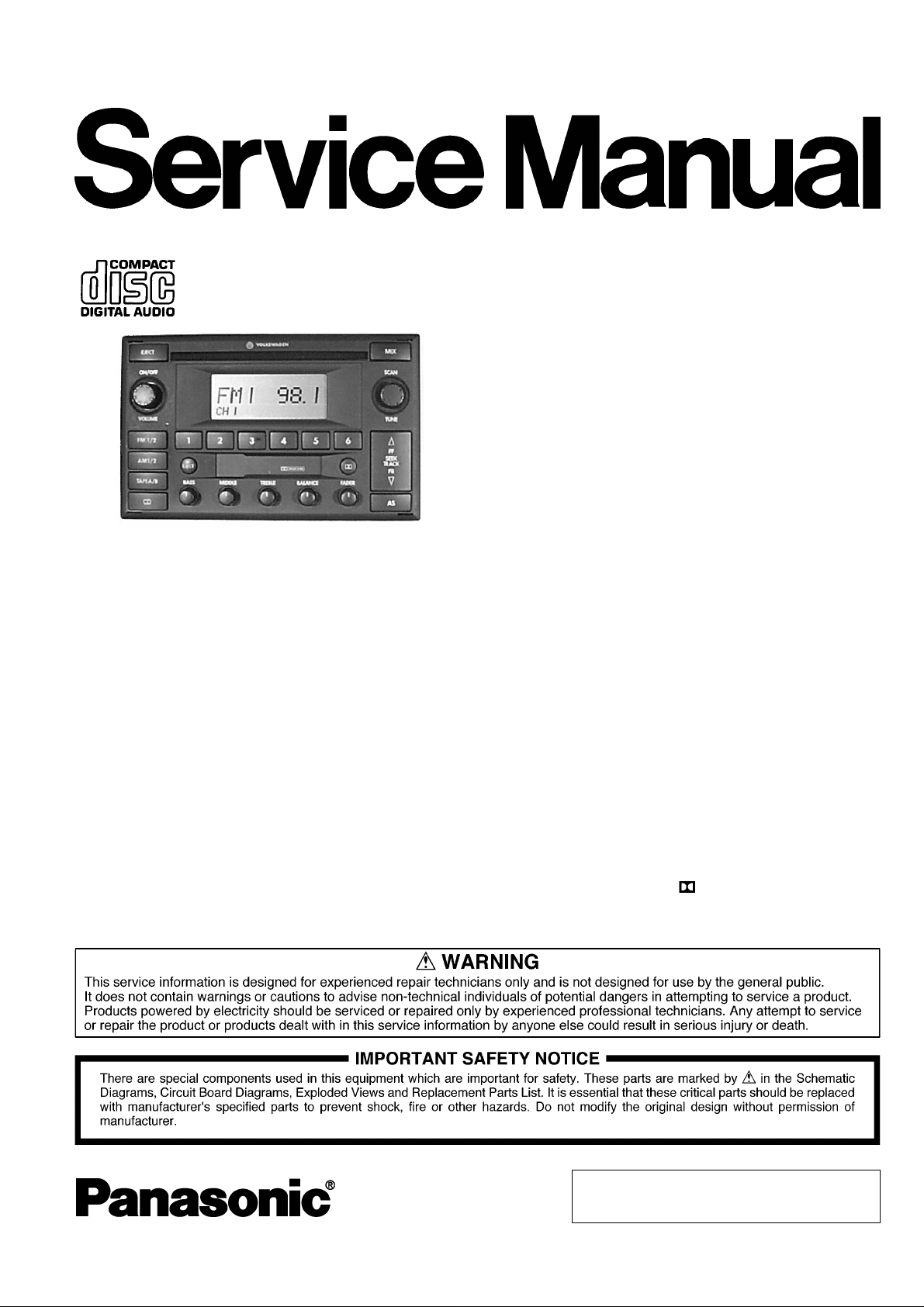
CQ-JV1060L
AM/FM MPX ELECTRONIC TUNING
RADIO with Stereo Cassette Tape
Player and CD Player
V.W. PART No. : 3B7 035 180
VEHICLE : PASSAT, GOLF, JETTA
DESTINATION : North America
PRODUCED AFTER : Aug., 2001
I0
Specification*
General
Power Supply DC 12V (11V - 16V),
Test Voltage 14.4V
Negative Ground
Current Consumption Less than 2.5A (0.5W×4ch)
Power Output 45W×4ch (at 0.5W)
Speaker Impedance 4Ω
AM Radio
Frequency Range 530 - 1,710kHz
Usable Sensitivity 23dB/µV (S/N 20dB)
FM Stereo Radio
Frequency Range 87.9 - 107.9MHz
Usable Sensitivity 4dB/µV (S/N 26dB)
CD Player
Decoding 16bit (Linear)
Signal to Noise Ratio More than 70dB (IHF-A)
Channel Separation More than 50dB (IHF-A)
Dimensions** 189(W)×111(H)×170(D)mm
Weight** 2.6kg
* Specifications and the design are subject to possible modification
without notice due to improvements.
** Dimensions and Weight shown are approximate.
Doldy noise reduction manufactured under license from Dolby
Laboratories Licensing Corporation.
“Dolby” and the double-D symbol
Laboratories Licensing Corporation.
are trade marks of Dolby
© 2001 Matsushita Communication Industrial Co.,
Ltd. All rights reserved. Unauthorized copying and
distribution is a violation of law.
V.W. / CQ-JV1060L
CONTENTS
Page Page
1 FEATUERS 2
2 LASER PRODUCTS
3 REAR VIEW
4 FRONT VIEW AND FUNCTIONS
5 WIRING CONNECTION
6 BLOCK DIAGRAM
7 TERMINALS DESCRIPTION
8 PACKAGE AND IC BLOCK DIAGRAM
9 REPLACEMENT PARTS LIST 13
2
10 EXPLODED VIEW (Unit)
11 CD PLAYER PARTS
2
3
12 EXPLODED VIEW (CD Deck)
4
13 TAPE PLAYER PARTS
14 EXPLODED VIEW (Tape Deck)
5
8
15 WIRING DIAGRAM
10
16 SCHEMAT IC DIAGRAM
21
22
23
24
25
26
35
1 FEATUERS
∙
PLL (Phase Locked Loop) synthesized tuning.
∙
12-FM, 12-AM presets with preset scan
∙
Dolby noise reduction.
∙
NCD-8 CD player.
∙
CD Changer control.
2 LASER PRODUCTS
3 REAR VIEW
2
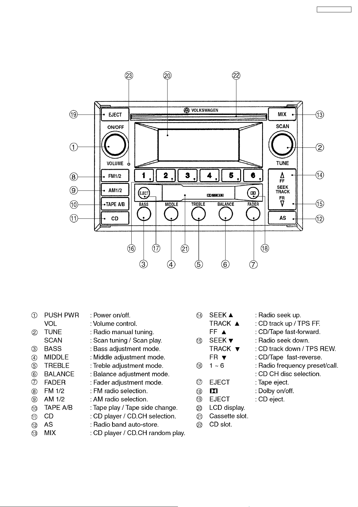
4 FRONT VIEW AND FUNCTIONS
V.W. / CQ-JV1060L
3
V.W. / CQ-JV1060L
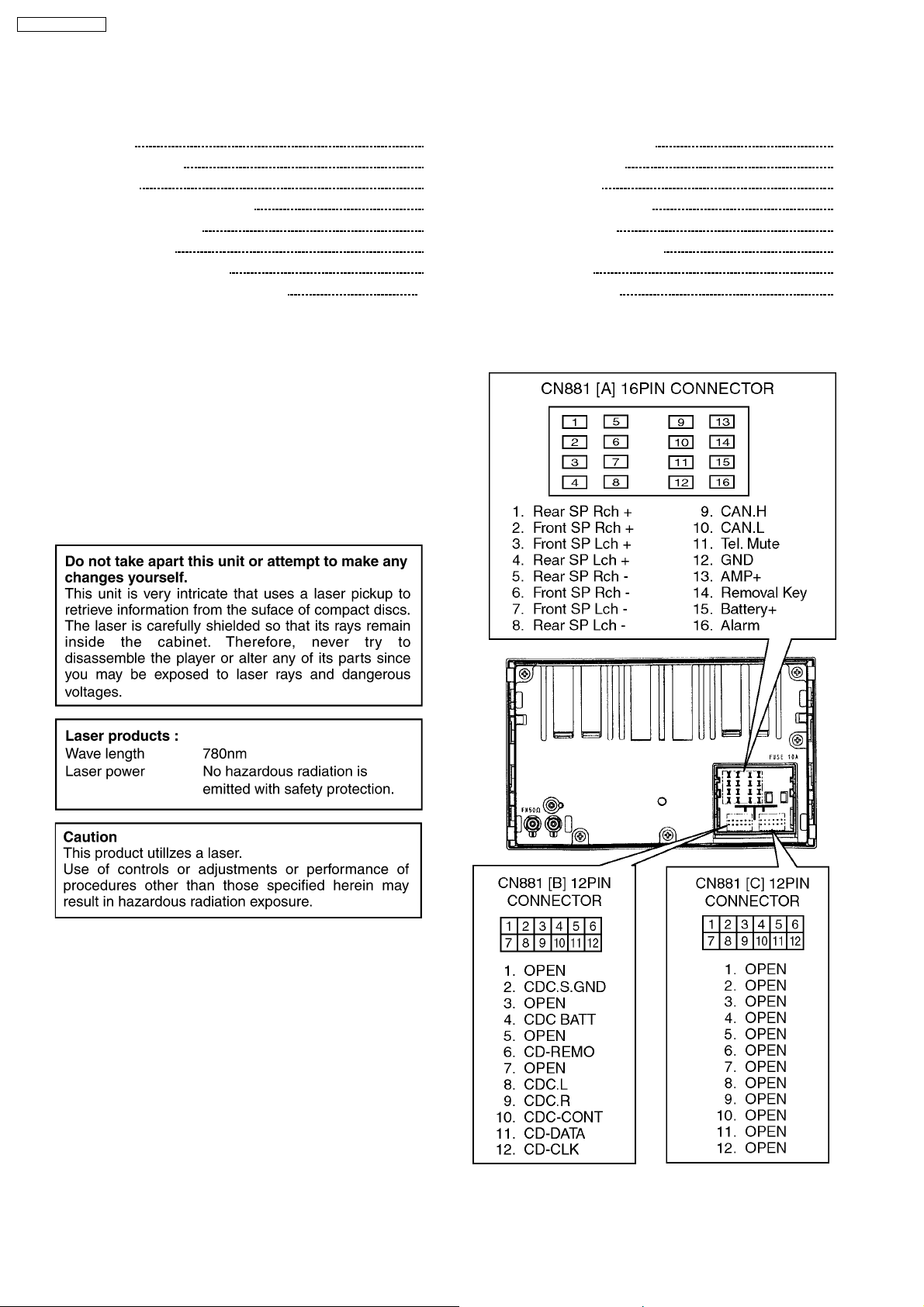
5 WIRING CONNECTION
4

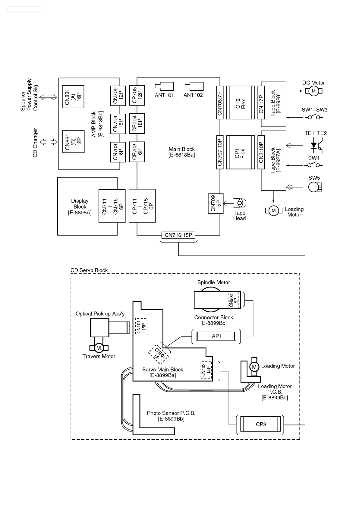
6 BLOCK DIAGRAM
6.1. Main Block
V.W. / CQ-JV1060L
5
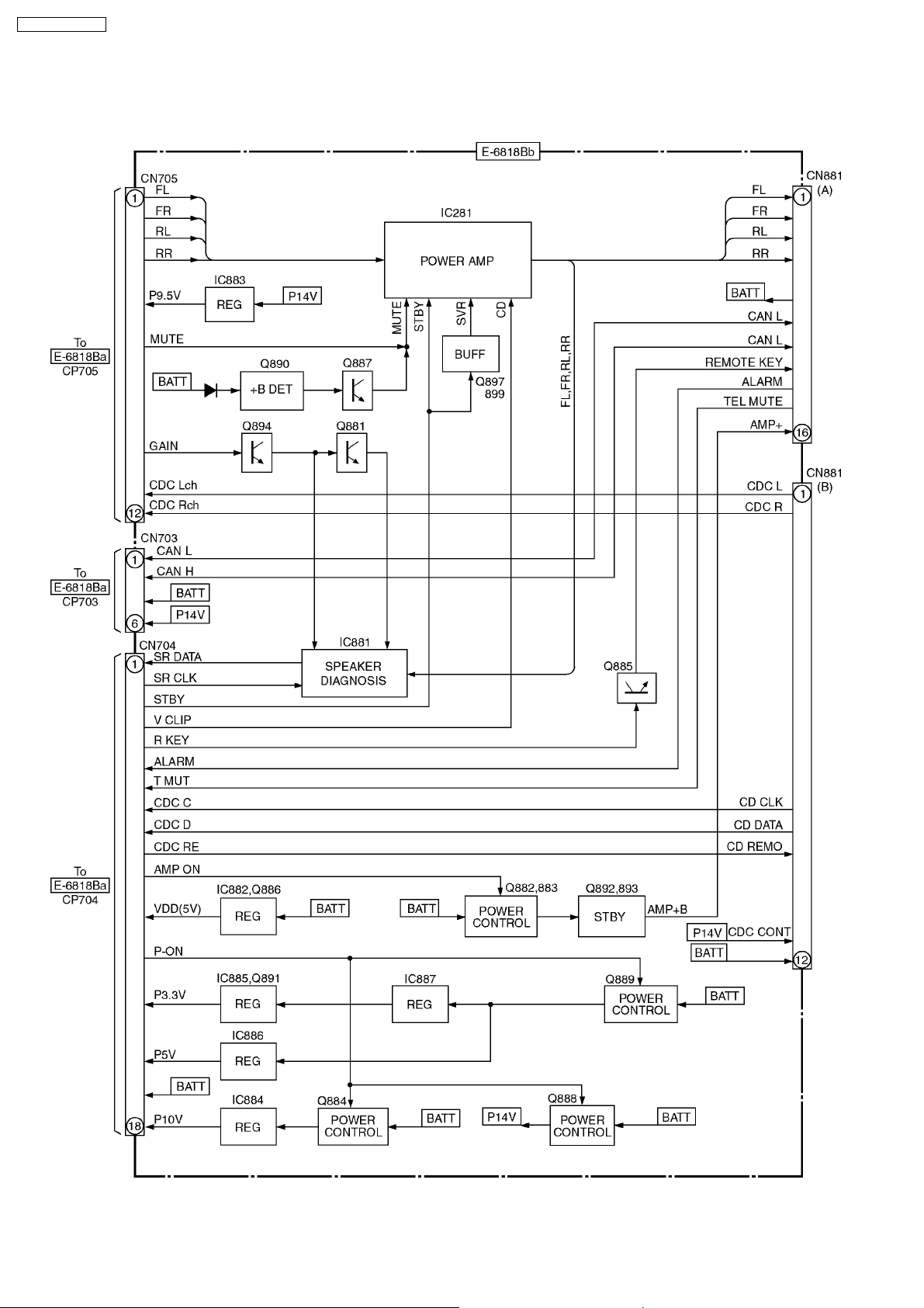
V.W. / CQ-JV1060L
6.2. AMP Block
6
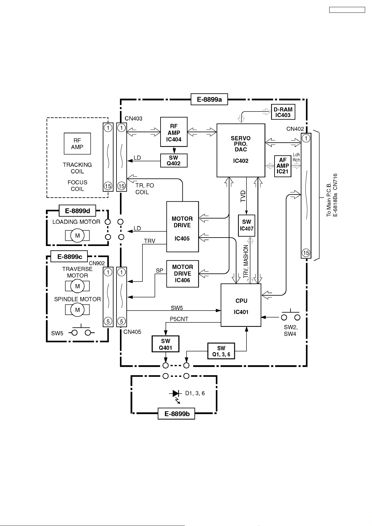
6.3. CD Servo Block
V.W. / CQ-JV1060L
7
V.W. / CQ-JV1060L
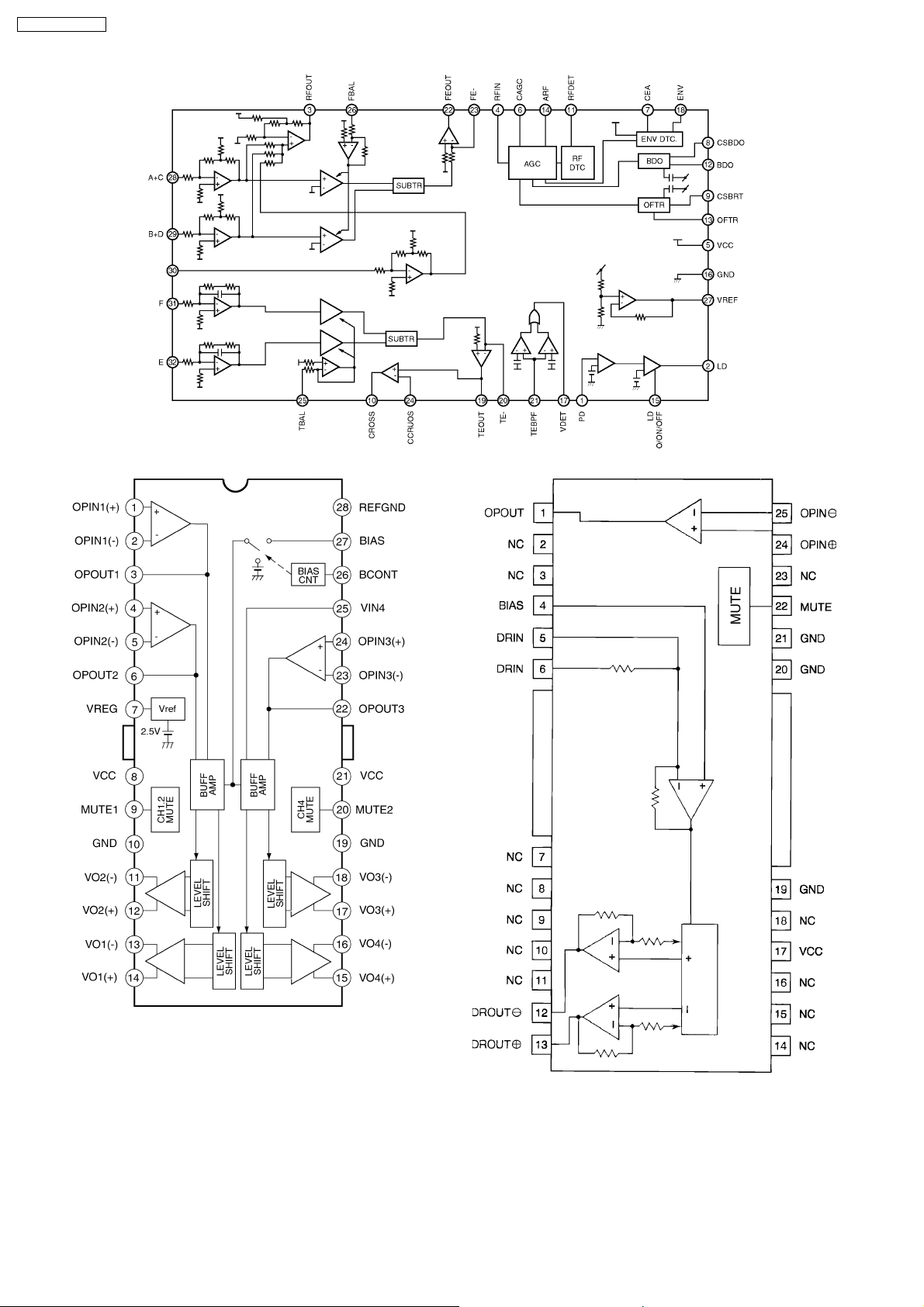
7 TERMINALS DESCRIPTION
7.1. Main Block
IC701 : C2CBKA00001
Pin
No.
1 RSTOUT Not used - 2 NMI (VDD pull-up) - 4.8
3 VSS Ground - 0
4 VDD +5V power supply - 4.8
5 LCD.ADR LCD addrress O 0
6 CD.SW3 CD disc out I 4.4
7 CD.SW1 CD disc in I 4.5
8 P.ON System power on O 4.8
9 CAN6.1V Battery level detection (6.1V) I 4.7
10 SAFE Safety LED control O 4.8
11 ILL2 Illumi. on (LCD) O 4.8
12 ILL Illumi. on (Button) O 4.8
13 KI0 Key data input I 0
14 KI1 Key data input I 0
15 KI2 Key data input I 0
16 KI3 Key data input I 0
17 VSS Ground - 0
18 VDD +5V power supply - 4.8
19 SR.DATA Serial data I/O 4.8
20 SR.CLK Clock for serial data O 4.8
21 ANT.CNT ANT1 amp power control O 0
22 A/B.IN Tape side detection I 4.7
23 TUN.A Tuning/Scan SW I 0
24 TUN.B Tuning/Scan SW I 0
25 VSS Ground - 0
26 VDD +5V power supply - 4.8
27 DEV FM deviation I 0
28 ADJ FM adjacent interference I 0
29 M.P FM multipath interference I 0
30 FILD Fieldstrength level I 0.5
31 IF.V ANT2 current intensity I 0.5
32 ANT.V ANT1 current intensity I 0.5
33 BATT.V Battery level detection I 2.6
34 FAD Fader level I 2.3
35 VA.REF +5V power supply - 4.8
36 VA.GND Ground - 0
37 BAL Balance level I 2.3
38 TRE Treble level I 0
39 MID Middle level I 1.0
40 BASS Bass level I 1.0
41 VSS Ground - 0
42 VDD +5V power supply - 4.8
43 BAT.DET Battery level detection I 4.8
44 CC.EJ Tape eject I 4.8
45 CD.EJ CD eject I 1.8
46 ALARM Alarm signal I 0
47 P.SW Power on SW I 4.8
48 CD.SW2 CD SW2 input I 0
49 T.LOAD Tape loading detection I 0
50 DIAG.CONT Not used - 51 VSS Ground - 0
52 VDD +5V power supply - 4.8
53 IF.ON ANT2 amp power control O 0
54 RADIO.ON Radio power control O 4.8
55 DSP.DET DSP in activity I 4.8
56 CD.RST CD reset O 4.8
57 CD.SIM0 CD serial data O 0
58 CD.ON CD controller enable O 0
59 BIT3 Tape mode SW I 0
60 BIT2 Tape mode SW I 0
61 CDC.REMO CD.CH remocon data O 0
62 CDC.DATA CD.CH data I 0
63 BIT1 Tape mode SW I 0
64 EQ Metal tape detection I
65 MS MS detection I 0
66 CDC.CLK Shift clock for CD.CH data O 0
67 LCD.DET LCD driver in activity I 0
Port Descriptions I/O Vol.
(V)
Pin
No.
68 VDD +5V power supply - 4.8
69 VSS Ground - 0
70 CD.SOMI CD serial data I 0
71 /T.MUT Telephon mute I 0
72 CD.SCKM Shift clock for CD data O 0
73 CAN.EN CAN BUS enable O 0
74 CAN.STB CAN BUS strobe O 0
75 CAN.RX CAN BUS data I 4.8
76 CAN.TX CAN BUS data O 4.8
77 CAN.N.ERR CAN BUS error I 4.8
78 VDD +5V power supply - 4.8
79 VSS Ground - 0
80 /RD Not used - 81 /WR Not used - 82 /READY Not used - 83 ALE Not used - 84 /EA (VDD pull-up) - 0
85 K00 Key scan O 1.2
86 K01 Key scan O 1.2
87 K02 Key scan O 0
88 K03 Key scan O 1.2
89 PL04 Not used - 90 R.IN Tape reverse O 0
91 T.IN Tape-in detection I 0
92 ENDA Tape end detection I 0
93 VDD +5V power supply - 4.8
94 VSS Ground - 0
95 CD.ON10V CD power on (10V) O 4.6
96 M2F Main motor control O 4.8
97 CC.ON Tape power on O 0
98 ENDB Tape end detection I 0
99 GAIN Audio output level control O 4.8
100 CD.ON5V CD power on (5V) O 4.8
101 F.IN Tape forword O 0
102 LCD.ON LCD driver reset O 4.8
103 E2DATA Security data I 0
104 ST-BY Power amp stand-by O 4.8
105 DSP.RST DSP reset O 4.8
106 AMP.ON External AMP power on O 0
107 MUT Not used - 4.8
108 M2 Main motor control O 0
109 VOL.A Volume control signal I 0
110 VOL.B Volume control signal I 0
111 VDD +5V power supply - 4.8
112 VSS Ground - 0
113 E2CE Security ROM chip enable O 0
114 LCD/E2 DT LCD/Security data O 0
115 LCD/E2 CK Clock for LCD/Security data O 0
116 LCD CS2 LCD driver select O 0
117 F/E.STP Radio stopsignal input I 0.9
118 F/E.DATA Tuner control data O 0
119 F/E.ENA Tuner enable O 0
120 F/E.CLK Shift clock for control data O 0
121 VDD +5V power supply - 4.8
122 VSS Ground - 0
123 XTAL2 Crystal oscillator - 2.0
124 XTAL1 Crystal osdillator - 2.3
125 VSS Ground - 0
126 XTAL3 Crystal oscillator - 2.3
127 XTAL4 Crystal oscillator - 2.3
128 RST Reset I 4.9
Port Descriptions I/O Vol.
(V)
Note 1 : Voltage measuerments are with respect to ground,
with a voltmeter (internal resistance : 10M ohms).
8
V.W. / CQ-JV1060L
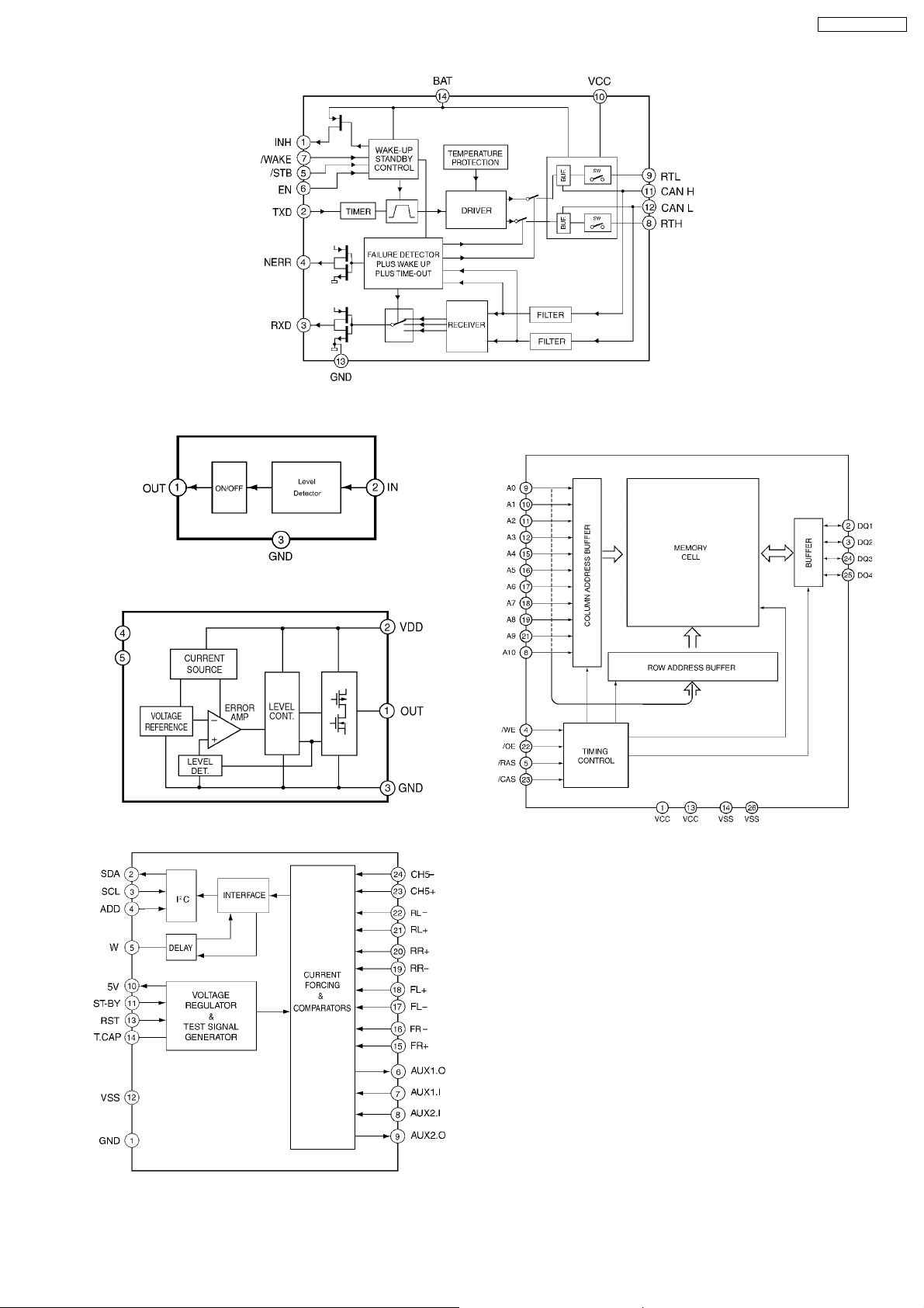
7.2. CD Servo Block
IC402 : MN662783RPW
Pin
No.
1 VDD +5V power supply - 5.0
2 D0 D-RAM data I/O 2.3
3 D1 D-RAM data I/O 1.8
4 NWE D-RAM data write O 4.9
5 NRAS D-RAM row address strobe O 3.4
6 D2 D-RAM data I/O 0.8
7 D3 D-RAM data I/O 0
8 NCAS0 D-RAM columun address strobe O 3.9
9 A10 D-RAM address O 3.9
10 A8 D-RAM address O 0.6
11 A7 D-RAM address O 1.1
12 A6 D-RAM address O 0.7
13 A5 D-RAM address O 0
14 A4 D-RAM address O 1.1
15 A9 D-RAM address O 0.4
16-18 A0 D-RAM address O 1.0
19 A3 D-RAM address O 0
20 DVSS Ground - 0
21 DVDD +5V power supply - 5.0
22,23 - Not used - -
24 TVD Traverse motor control O 2.5
25 PC Not used - 26 ECS Spindle motor control O 2.4
27 TRD Tracking coil drive O 2.5
28 FOD Focus coil drive O 2.4
29 FBAL Focus balance O 1.9
30 TBAL Tracking balance O 3.0
31 VREF Refence voltage I 2.5
32 FE Focus error I 2.5
33 TE Tracking error I 2.5
34 RFENV RF envelope I 2.5
35 OFTR Off track signal I 0
36 /RFDET RF detecting signal I 0
37 BDO Drop-out signal I 0
38 LDON Laser on signal O 4.5
39 ARF RF signal I 2.5
40 IREF Reference current input I 1.2
41 DRF Bias for DSL I 2.4
42 DSLF Loop filter for DSL I/O 2.5
43 DSLF2 Loop filter for DSL I/O 2.2
44 PLLF Loop filter for PLL I/O 1.4
45 VCOF Not used - 46 AVDD +5V power supply - 5.0
47 AVSS Ground - 0
48 OUTL L channel output O 2.3
49 AVSS Ground - 0
50 OUTR R channel output O 2.3
51 AVDD +5V power supply - 4.7
52-54 - (Connecting to ground) - 0
55 FLAG Flag output O 0
56 FCLK Frame clock O 0
57-59 - Not used - -
60 TX Not used - 61 MCLK Clock for I/F command I 1.0
62 MDATA Date for I/F command I 3.1
63 MLD I/F command load I 5.0
64 BLKCK Subcode block clock O 0
65 SQCK Ext.clock for sub code-Q I 5.0
66 SUBQ Code for sub. code-Q O 3.8
67 DMUTE Mute input I 0
68 STAT Status signal O 5.0
69 NRST Reset input I 5.0
70 CSEL (Connecting to ground) - 0
71 PMCK Clock output O 2.5
72 SMCK Clock output O 2.5
73 SUBC Serial data of sub code O 0
74 SBCK Shift clock for SUBC I 0.6
75 NCLDCK Not used - 76 NTEST (Connecting to VDD) - 5.0
Port Descriptions I/O Vol.
(V)
Pin
No.
77 X1 Crystal oscillator - 0.4
78 X2 Crystal oscillator - 3.2
79 DVDD +5V power supply - 5.0
80 DVSS Ground - 0
Port Descriptions I/O Vol.
IC401 : MN101C30AAE
Pin
No.
1 SW4 Disc clamp detection I 0
2 SW5 Inner track detection I 5.0
3 SW2 Feeder arm detection I 4.8
4 PAG (Connecting to ground) - 0
5 IFR (Connecting to ground) - 0
6 VREF+ +5V power supply - 5.0
7 VDD +5V power supply - 5.0
8 OSC2 Crystal oscillator - 2.2
9 OSC1 Crystal oscillator - 2.1
10 VSS Ground - 0
11 XI (Connecting to ground) - 0
12 XO Not used - 13 GND Ground - 0
14 SOMI CD changer serial data O 4.3
15 SIMO CD changer serial data I 1.3
16 SCKM Clock for serial data I 5.0
17 SB01 Not used - 18 SUBQ Code for sub. code-Q I 1.6
19 SQCK Ext. clock for sub. code-Q O 5.0
20 P0G Not used - 21 RST Reset input I 4.9
22 BD0 Drop-out signal I 0
23 PC1 Loading motor driver control O 5.0
24-26 - Not used - -
27 CDON CD activity I 5.0
28 BLKCK Subcode block clock O 0
29-31 - Not used - -
32 PC2 Focus/Tracking driver control O 0
33-36 - Not used - -
37 LOD Loading motor control I/O 2.5
38 TRV Traverse motor control I/O 2.4
39 NRST Servo IC reset O 5.0
40 STAT Status signal I 2.1
41 DMUTE DSP mute O 0
42-55 - Not used - -
56 MASHON Servo IC OSC control O 0.2
57 MCLK Command clock O 4.1
58 MDATA Command data O 3.1
59 MLD Command load O 5.0
60 P80 Not used - 61 VREF- (Connecting to ground) - 0
62 Q1 Photo sensor signal (DISC IN) I 4.5
63 Q3 Photo sensor signal (DISC OUT) I 4.2
64 Q6 Photo sensor signal (Option) I 5.0
Port Descriptions I/O Vol.
(V)
(V)
9
V.W. / CQ-JV1060L
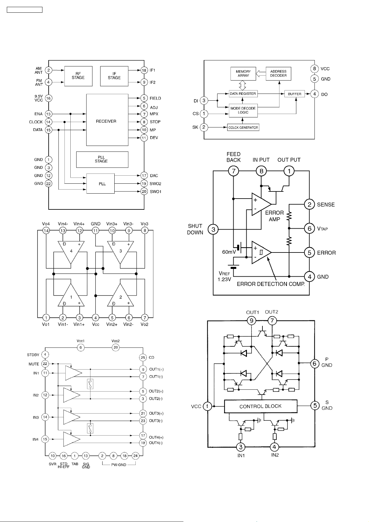
8 PACKAGE AND IC BLOCK DIAGRAM
8.1. Main Block
IC705 : YEAMS2922ADF
PA101 : J3CCAB000001
IC102 : AN6564NST1
IC706 : YEAM2951MT
IC281 : C1BA00000314
IC710 : YEAMLB1930MT
10
IC707 : C1EB00000039
8.2. CD Servo Block
V.W. / CQ-JV1060L
IC714 : MN1382QTX
IC715 : C0EBM0000005
IC403 : C3ABMB000022
IC881 : C1EB00000042
11
V.W. / CQ-JV1060L
IC404 : C1BB00000173
IC405 : C0GBY0000004
IC406 : C0GBY0000003
12
 Loading...