

Page 1

SERVICE MANUAL
DVD Video Recorder
FILE NO. 810-200604GR
REVISED.01
®
D-RW2SU
The above model is classified as a green product (*1), as indicated by the underlined serial
number. This Service Manual describes replacement parts for the green product. When
repairing this green product, use the part(s) described in this manual and lead-free solder (*2).
For (*1) and (*2), see the next page.
TOSHIBA CORPORATION 2006
Published in Japan, Feb. 2006 GREEN
Page 2
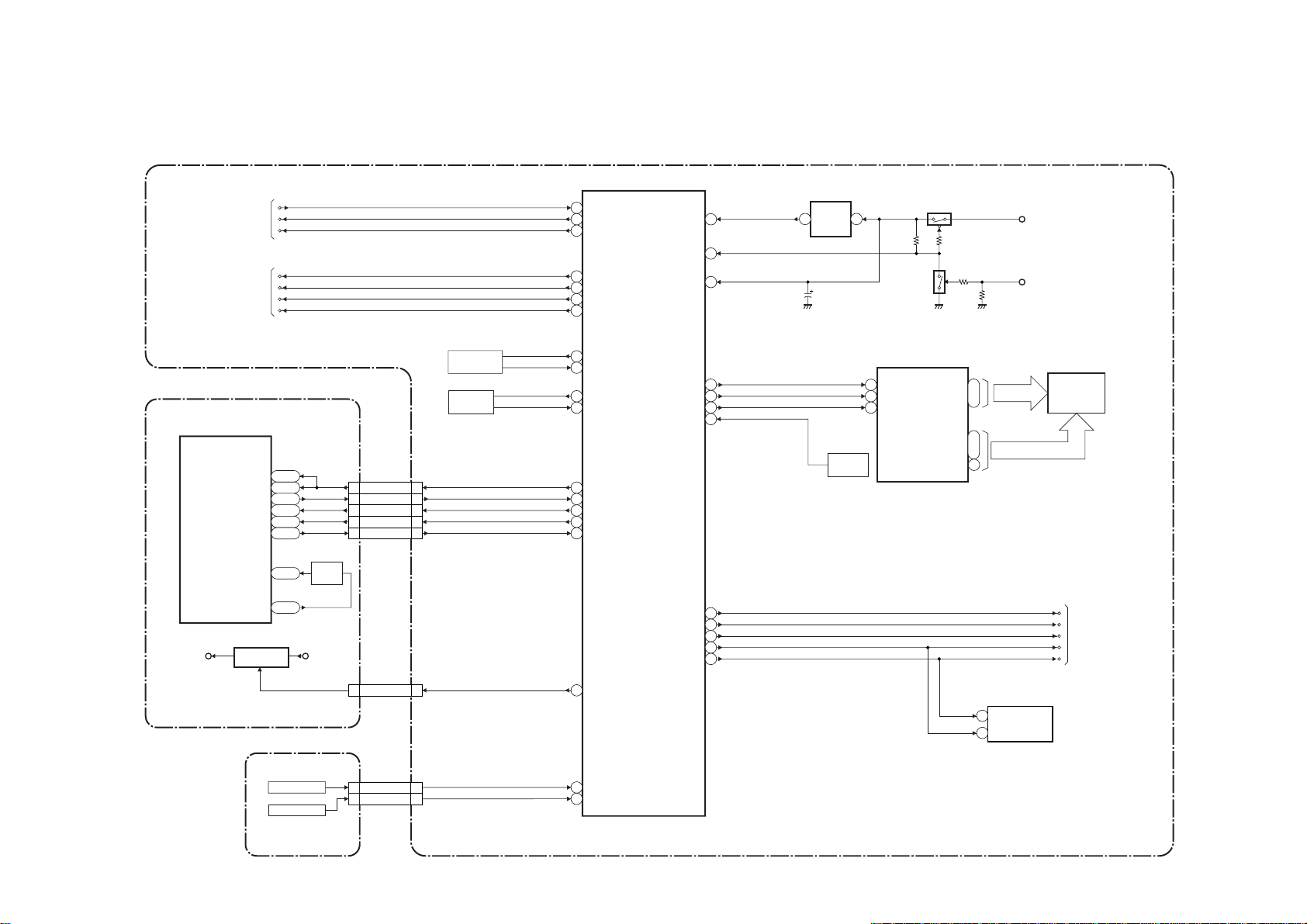
System Control Block Diagram
NOTE: BOARD MEANS PRINTED CIRCUIT BOARD.
TO POWER SUPPLY
BLOCK DIAGRAM
TO VIDEO
BLOCK DIAGRAM
POW-SW
REG-CONT
PWSW
VIDEO-SW1
VIDEO-SW2
VIDEO-SW3
VIDEO-MUTE
BLOCK DIAGRAMS
IC1501
(SUB MICRO CONTROLLER)
3
POW-SW
52
REG-CONT
53
PWSW
41
VIDEO-SW1
42 VIDEO-SW2
43 VIDEO-SW3
44 VIDEO-MUTE
RESET
P-DOWN
VCC
14
30
7
IC1502
RESET
1 2
C1501
(BACKUP CAPACITOR)
Q1502
Q1501
EV+3.3V
EV+5V
IC101
(MAIN MICRO CONTROLLER)
SYS-RESET
SYS-RESET
SUB-RXD
SUB-TXD
SUB-SCLK
CLK 27 IN
CLK 27 OUT
RDY
IC106
+1.2V
REGULATOR
J25
N23
N24
L25
R24
DVD MAIN BOARD
KEY SWITCH
KEY SWITCH
X1501
8MHz
RESONATOR
X1502
32.768KHz
X'TAL
T4
N2
N1
CN701
44SYS-RESET
11SUB-RXD
33SUB-TXD
55SUB-SCLK
22RDY
X552
27MHz
X'TAL
VI+1.2VP-ON+1.2V
CN101 CN1051
30 301V2CONT
CN3001
KEY-1
1
KEY-2
2
CN1101
CN1502
1
2
8
X OUT
9
X IN
12
XC OUT
XC IN
11
22
SYS-RESET
19
SUB-RXD
18
SUB-TXD
20
SUB-SCLK
RDY
29
26
1V2CONT
1
KEY-1
2
KEY-2
FL-SDA
FL-SCL
FL-STB
REMOTE
AUDIO-MUTE
AUDIO-SW1
AUDIO-SW2
SDA
SCL
IC2001
(VFD DRIVER)
1G
48
50
49
27
38
40
39
33
34
RE2001
REMOTE
SENSOR
28
DIN
1
CLK
2
STB
23
~
~
7G
17
a
7
~
~
h
14
i
16
TU1701(TUNER UNIT)
10
11
AUDIO-MUTE
SCL
SDA
GRID
SEGMENT
AUDIO-SW1
AUDIO-SW2
SDA
SCL
FL2001
VFD
TO AUDIO
BLOCK DIAGRAM
BOARD SWITCH
BOARD POWER
1-10-1
E7A70BLS
Page 3
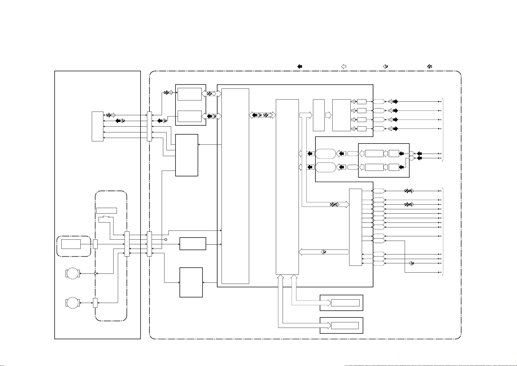
Digital Signal Process Block Diagram
NOTE: BOARD MEANS PRINTED CIRCUIT BOARD.
DVD MECHANISM
FE
ENCODER
ENCODER BOARD
SLED
MOTOR
M
SPINDLE
MOTOR
M
PICK
-UP
TRAY OPEN
CN1003
CN1002
TILT
TRACKING
FOCUS
CN1001
CN201
CN301
+3.3V
IC201
RF/
ERROR AMP
IC301
MOTOR
DRIVER
IC202
OP AMP
IC302
MOTOR
DRIVER
LPC
IC101
FRONT-END
DIGITAL
SIGNAL
PROCESS
BACK-END
DIGITAL
SIGNAL
PROCESS
REC VIDEO SIGNAL PB VIDEO SIGNAL REC AUDIO SIGNAL PB AUDIO SIGNAL
VIDEO-Y(I/P)
VIDEO-Cb/Pb
VIDEO-Cr/Pr
VIDEO-Y/CVBS
10
13
VIDEO-C
VIDEO-C
SPDIF
BCK
DATA
LRCK
AIMS
MD
MC
MS
SCK
LRCK
BCK
DATA
SYSCLK
TO VIDEO
BLOCK
DIAGRAM
TO AUDI O
BLOCK
DIAGRAM
VIDEO
I/F
VIDEO
ENCODER
Y2, AA4,
AB1-AB4
V3, Y3, W1,
Y4, W2, AA3
IC104 (FLASH MEMORY)
FLASH MEMORY
D/A
G4
D/A
L4
K1
D/A
G3
D/A
IC701 (VIDEO DECODER)
DECODER A/D45-50
DECODER A/D39-44
T2
U1
R3
U2
R26
M25
AUDI O
I/F
K26
P24
T3
R2
P2
R1
P3
RELAY BOARD
DVD MAIN BOARD
1-10-2
IC102 (DDR SDRAM)
DDR SDRAM
E7A70BLD
Page 4
NOTE: BOARD MEANS PRINTED CIRCUIT BOARD.
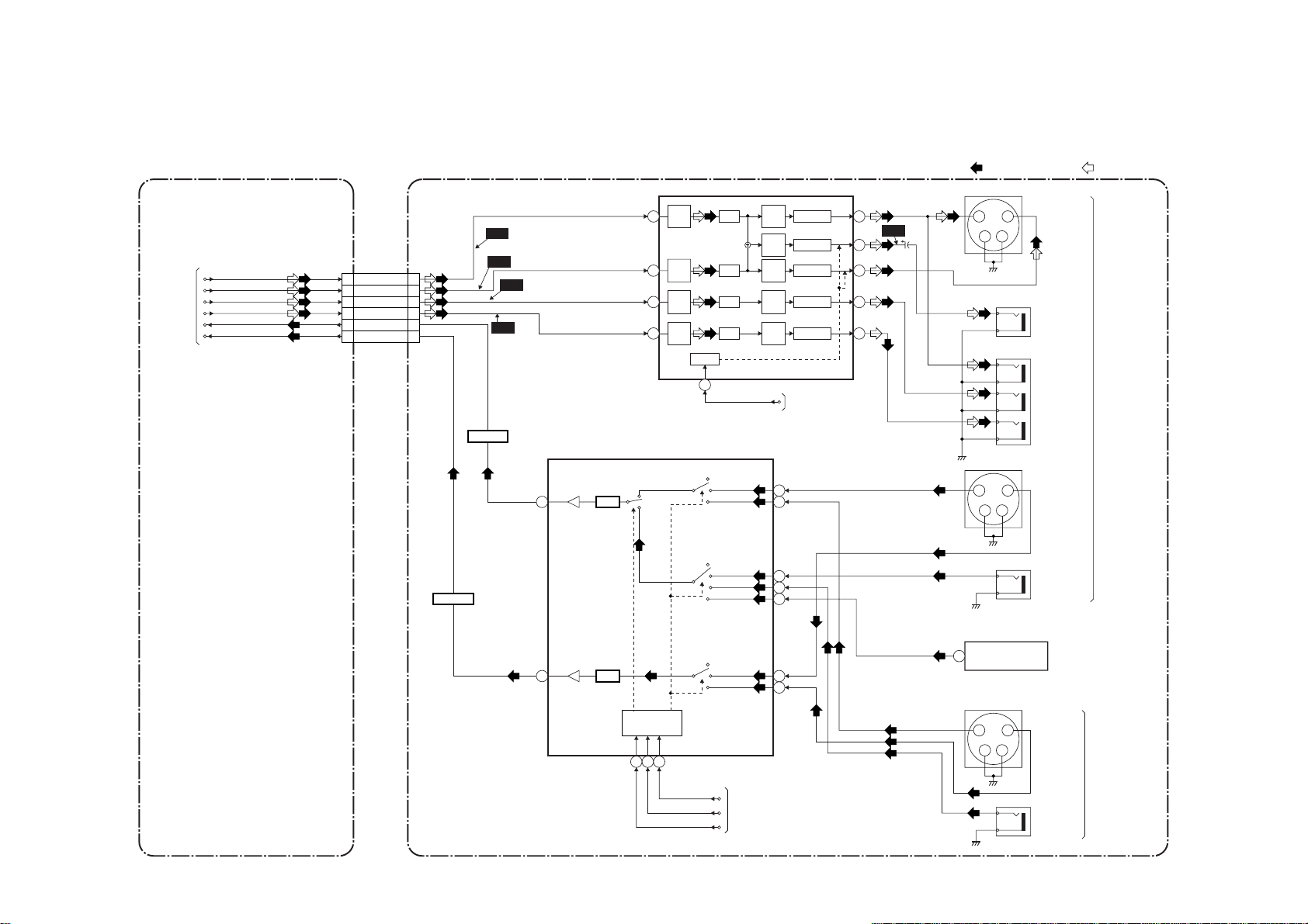
Video Block Diagram
VIDEO-Y(I/P)
TO DIGITAL
SIGNAL
PROCESS
BLOCK
DIAGRAM
VIDEO-C
VIDEO-Cb/Pb
VIDEO-Cr/Pr
VIDEO-Y/CVBS
VIDEO-C
CN701
24 24
VIDEO-Y(I/P)-OUT
22 22
VIDEO-C-OUT
28 28
VIDEO-Cb/Pb-OUT
26 26
VIDEO-Cr/Pr-OUT
10 10
VIDEO-Y/CVBS-IN
88VIDEO-C-IN
CN1101
Q1304
BUFFER
WF1
WF2
WF5
WF4
IC1301
19
3
1
6
8
(VIDEO INPUT SELECT)
LPF
IC1401 (VIDEO DRIVER)
4dB
AMP
4dB
AMP
4dB
AMP
4dB
AMP
LPF DRIVER
-6dB
LPF DRIVER
LPF DRIVER
LPF
MUTE
5
VIDEO-MUTE TO SYSTEM CONTROL
MUTE
Y1
Y2
2dB
AMP
8dB
AMP
2dB
AMP
2dB
AMP
2dB
AMP
BLOCK DIAGRAM
13
15
DRIVER
DRIVER
REC VIDEO SIGNAL PB VIDEO SIGNAL
Y
13
WF3
14
C1418
15
11
10
3 4
YC
3 4
C
JK2202
S-VIDEO
2
JK2201
JK2203
2
OUT
VIDEO-OUT
VIDEO-Y
OUT
VIDEO-Cb/Pb
OUT
VIDEO-Cr/Pr
OUT
JK2105
S-VIDEO
IN1
REAR
1
1
Q1303
BUFFER
MUTE
VIDEO1
VIDEO2
TUNER
MUTE
VIDEO-SW1
VIDEO-SW2
VIDEO-SW3
C1
C2
21
LPF
CONTROL
LOGIC
22 23
24
8
10
12
2
4
TO SYSTEM CONTROL
BLOCK DIAGRAM
JK2106
VIDEO-IN1
TU1701 (TUNER UNIT)
17
TU-VIDEO
YC
3 4
1
2
JK2102
JK2101
S-VIDEO
IN2
VIDEO IN2
FRONT
BOARD POWERDVD MAIN BOARD
1-10-3
E7A70BLV
Page 5
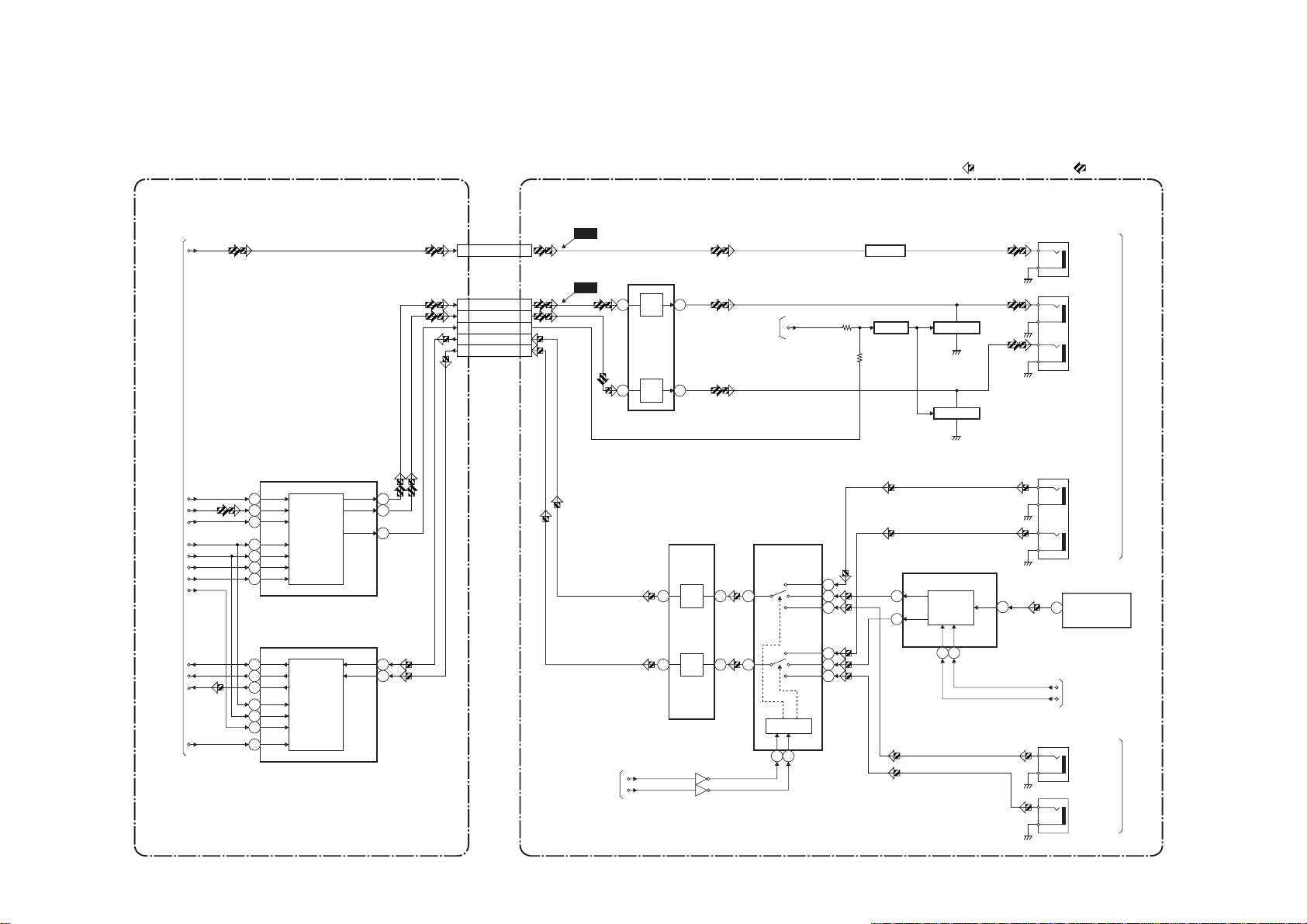
Audio Block Diagram
NOTE: BOARD MEANS PRINTED CIRCUIT BOARD.
REC AUDIO SIGNAL PB AUDIO SIGNAL
TO DIGITAL
SIGNAL
PROCESS
BLOCK
DIAGRAM
SPDIF
BCK
DATA
LRCK
MD
MC
MS
SCK
AIMS
LRCK
BCK
DATA
SYSCLK
IC801 (AUDIO D/A CONVERTER)
7
6
8
AUDIO D/A
CONVERTER
4
3
2
5
IC802 (AUDIO A/D CONVERTER)
7
8
9
AUDIO A/D
10
CONVERTER
11
12
6
MUTE
L-CH
R-CH
L-CH
R-CH
CN101 CN1051
28 28SPDIF
CN701 CN1101
14 14
AUDIO(L)-OUT
16 16
AUDIO(R)-OUT
12 12
DVD-AUDIO-MUTE
20 20
AUDIO(L)-IN
18 18
AUDIO(R)-IN
15
14
16
13
14
TO SYSTEM CONTROL
BLOCK DIAGRAM
WF7
WF6
2
6
IC1201
OP AMP
(
)
OP
AMP
OP
AMP
IC1102
(
1
7
AUDIO-SW2
AUDIO-SW1
1
TO
SYSTEM CONTROL
BLOCK DIAGRAM
7
OP AMP
)
OP
AMP
OP
AMP
Q1102
Q1101
IC1101
(AUDIO INPUT SELECT)
13
2
3
6
(L-CH)
(R-CH)
SW CTL
9 10
AUDIO-MUTE
IN1
TU
IN2
IN1
TU
IN2
Q1241
BUFFER
Q1203 Q1201
11
15
14
4
2
5
MUTE-ONDRIVE
Q1202
MUTE-ON
IC1701
MTS/SAP AUDIO
(
SIGNAL PROCESS
L-CH
MTS/SAP
30
AUDIO
SIGNAL
R-CH
29
PROCESS
24 27
)
21
JK2201
JK2106
SCL
SDA
JK2103
JK2104
JK2206
TU1701
14
SIF OUT
DIGITAL
AUDIO OUT
(COAXIAL)
AUDIO(L)
-OUT1
AUDIO(R)
-OUT1
REAR
AUDIO(L)
-IN1
AUDIO(R)
-IN1
(TUNER UNIT)
TO SYSTEM CONTROL
BLOCK DIAGRAM
AUDIO(L)
-IN2
FRONT
AUDIO(R)
-IN2
BOARD POWERDVD MAIN BOARD
1-10-4
E7A70BLA
Page 6
Power Supply Block Diagram
NOTE: BOARD MEANS PRINTED CIRCUIT BOARD.
CAUTION !
Fixed voltage (or Auto voltage selectable) power supply circuit is used in this unit.
If Main Fuse (F1001) is blown , check to see that all components in the power supply
circuit are not defective before you connect the AC plug to the AC power supply.
Otherwise it may cause some components in the power supply circuit to fail.
HOT CIRCUIT. BE CAREFUL.
AC1001
AC CORD
F1001
1A 250V
L1001
LINE
FILTER
D1001-D1004
BRIDGE
RECTIFIER
F
A V
Q1002
SW
Q1003
SW
CTL
Q1001
SW
CTL
T1001
8
6
3
4
IC1001
ERROR
VOLTAGE DET
4 1
F
A V
20
19
18
17
16
15
14
13
12
11
CAUTION !
For continued protection against fire hazard,
replace only with the same type fuse.
ATTENTION : Pour une protection continue les risqes
d'Incele n'utiliser que des fusible de même type.
Risk of fire-replace fuse as marked.
"This symbol means fast operating fuse."
"Ce symbole reprèsente un fusible à fusion rapide."
D1063
RECTIFIER
D1058
RECTIFIER
D1055
RECTIFIER
D1056
RECTIFIER
D1068
RECTIFIER
D1054
RECTIFIER
D1051
RECTIFIER
Q1055
Q1054
SW+10.5V
Q1063
SW+3.3V
J1215
Q1056
Q1053
SW+5V
Q1505
NOTE:
The voltage for parts in hot circuit is measured using
hot GND as a common terminal.
CN1051
4-6 EV+10.5V
9-11
P-ON+5V
14-16
P-ON+3.3V
19-21
VI+1.2V
24,25
P-ON+2.5V(1)
IC1504
+2.5V
1 2
REG.
4
REG-CONT
PWSW
POW-SW
FAN+10.5V
EV+3.3V
TUNER+5V
VIDEO+5V
P-ON+10.5V
EV+5V
EV+32V
Q1065
Q1057
SW+5V
IC1503
+3.3V
1 2
REG.
4
SW+5V
TO DVD MAIN
BOARD CN101
TO
SYSTEM CONTROL
BLOCK DIAGRAM
HOT
3
2
COLD
BOARD POWER
1-10-5
F2
-FL
F1
E7A70BLP
Page 7

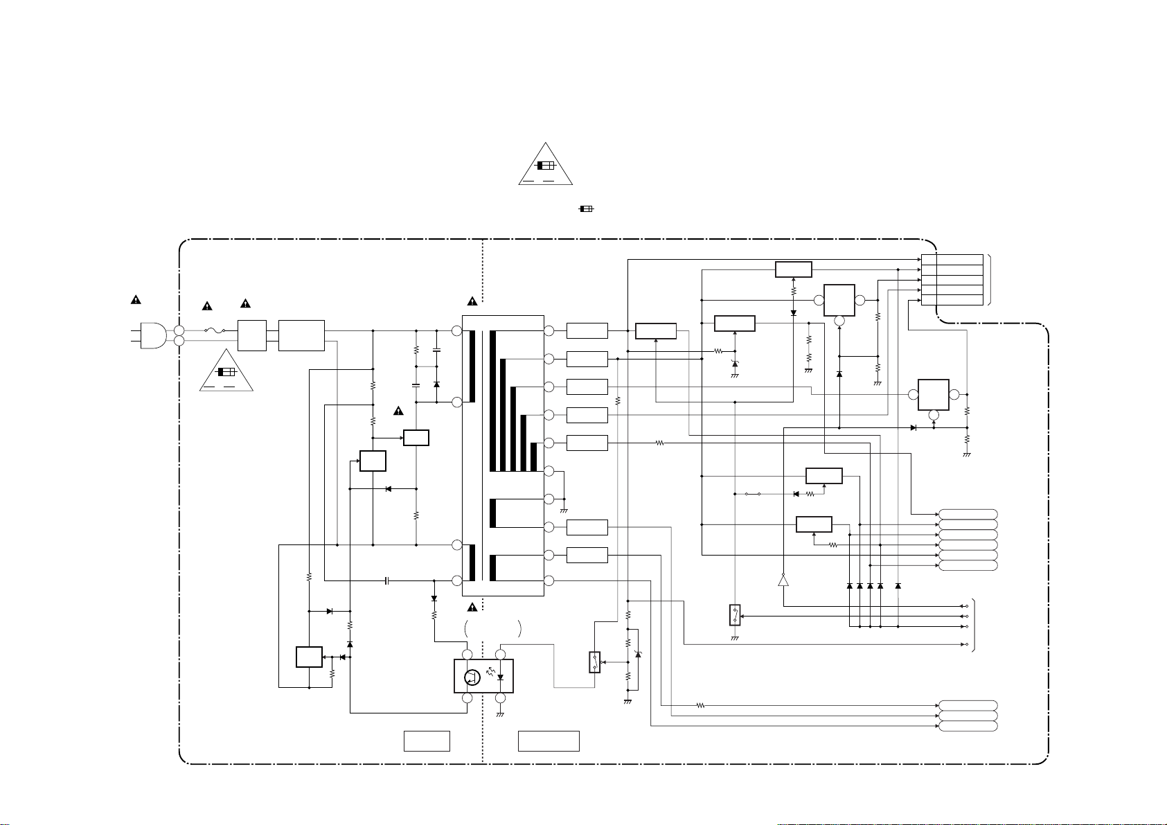
SCHEMATIC DIAGRAMS / BOARD’S AND TEST POINTS
NOTE: BOARD MEANS PRINTED CIRCUIT BOARD.
Standard Notes
WARNING
Many electrical and mechanical parts in this chassis
have special characteristics. These characterist ics
often pass unnoticed and the protection afforded by
them cannot necessarily be obtained by using
replacement components rated for higher voltage,
wattage, etc. Replacement parts that have these
special safety characteristics are identified in this
manual and its supplements; electrical components
having such features are identified by the mark “#” in
the schematic diagram and the parts list. Before
replacing any of these components, read the parts list
in this manual carefully. The use of substitute
replacement parts that do not have the same safety
characteristics as specified in the parts list may create
shock, fire, or other hazards.
Notes:
1. Do not use the part number shown on these
drawings for ordering. The correct part number is
shown in the parts list, and may be slightly
different or amended since these drawings were
prepared.
2. All resistance values are indicated in ohms
(K = 10
3. Resistor wattages are 1/4W or 1/6W unless
otherwise specified.
4. All capacitance values are indicated in µF
(P = 10
5. All voltages are DC voltages unless otherwise
specified.
3
, M = 106).
-6
µF).
1-11-1 R2N_SC
Page 8
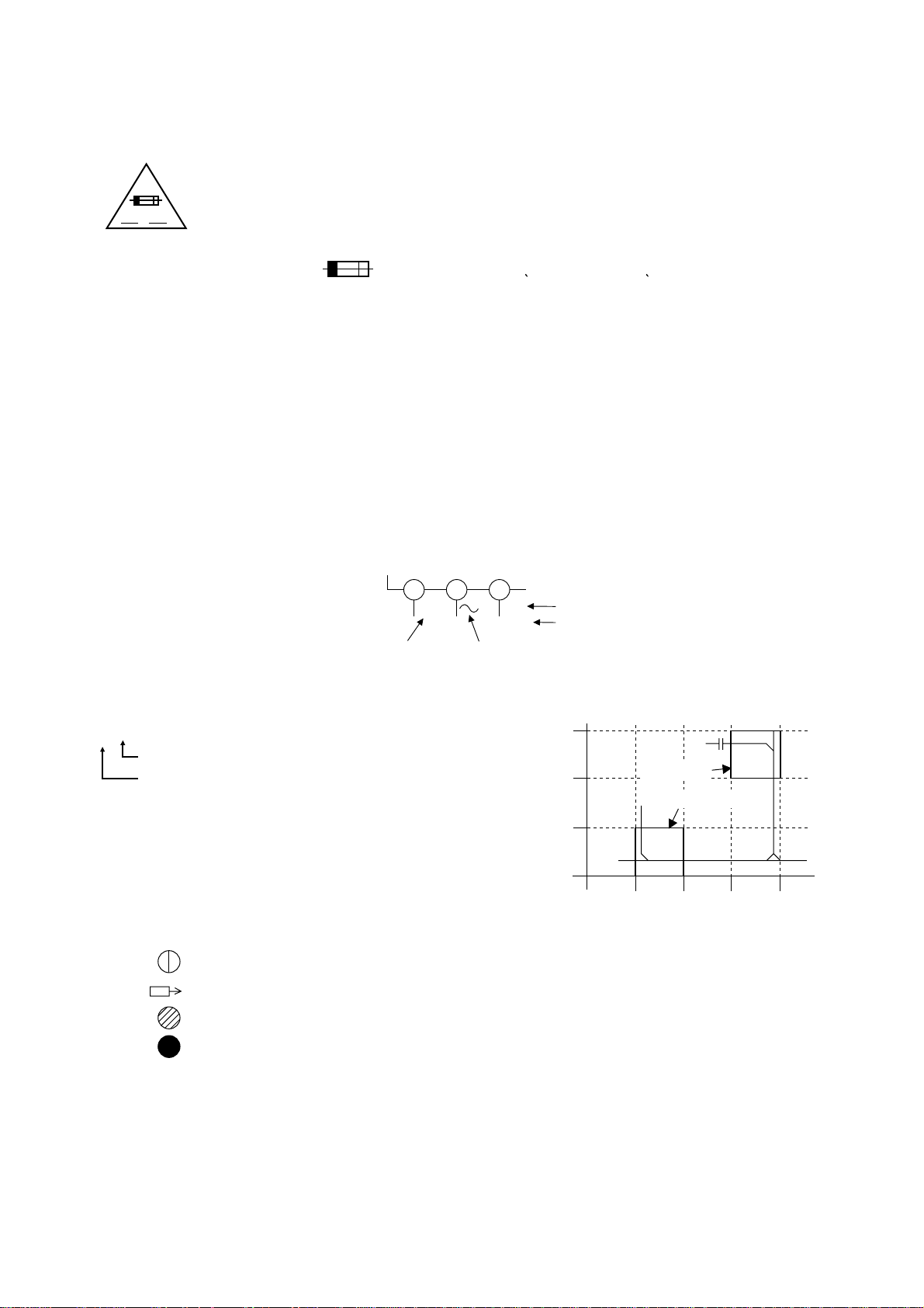
LIST OF CAUTION, NOTES, AND SYMBOLS USED IN THE SCHEMATIC DIAGRAMS ON
THE FOLLOWING PAGES:
1. CAUTION:
FOR CONTINUED PROTECTION AGAINST FIRE HAZARD, REPLACE ONLY WITH THE
F
A V
SAME TYPE FUSE.
ATTENTION: POUR UNE PROTECTION CONTINUE LES RISQES D'INCELE N'UTILISER
QUE DES FUSIBLE DE MÊME TYPE.
RISK OF FIRE-REPLACE FUSE AS MARKED.
This symbol means fast operating fuse.
Ce symbole represente un fusible a fusion rapide.
2. CAUTION:
Fixed Voltage (or Auto voltage selectable) power supply circuit is used in this unit.
If Main Fuse (F1001) is blown, first check to see that all components in the power supply circuit are not
defective before you connect the AC plug to the AC power supply. Otherwise it may cause some components
in the power supply circuit to fail.
3. Note:
1. Do not use the part number shown on the drawings for ordering. The correct part number is shown in the
parts list, and may be slightly different or amended since the drawings were prepared.
2. To maintain original function and reliability of repaired units, use only original replacement parts which are
listed with their part numbers in the parts list section of the service manual.
4. Voltage indications for PLAY and REC mode on the schematics are as shown below:
2
1
(Unit: Volt)
The same voltage for
both PLAY & REC modes
5.0
3
5.0
(2.5)
Indicates that the voltage
is not consistent here.
PLAY mode
REC mode
5. How to read converged lines
1-D3
Distinction Area
Line Number
(1 to 3 digits)
3
1-B1
AREA D3
2
AREA B1
Examples:
1. "1-D3" means that line number "1" goes to the line number
"1" of the area "D3".
1
1-D3
2. "1-B1" means that line number "1" goes to the line number
"1" of the area "B1".
ABCD
6. Test Point Information
: Indicates a test point with a jumper wire across a hole in the BOARD.
: Used to indicate a test point with a component lead on foil side.
: Used to indicate a test point with no test pin.
: Used to indicate a test point with a test pin.
1-11-2 R2N_SC
Page 9
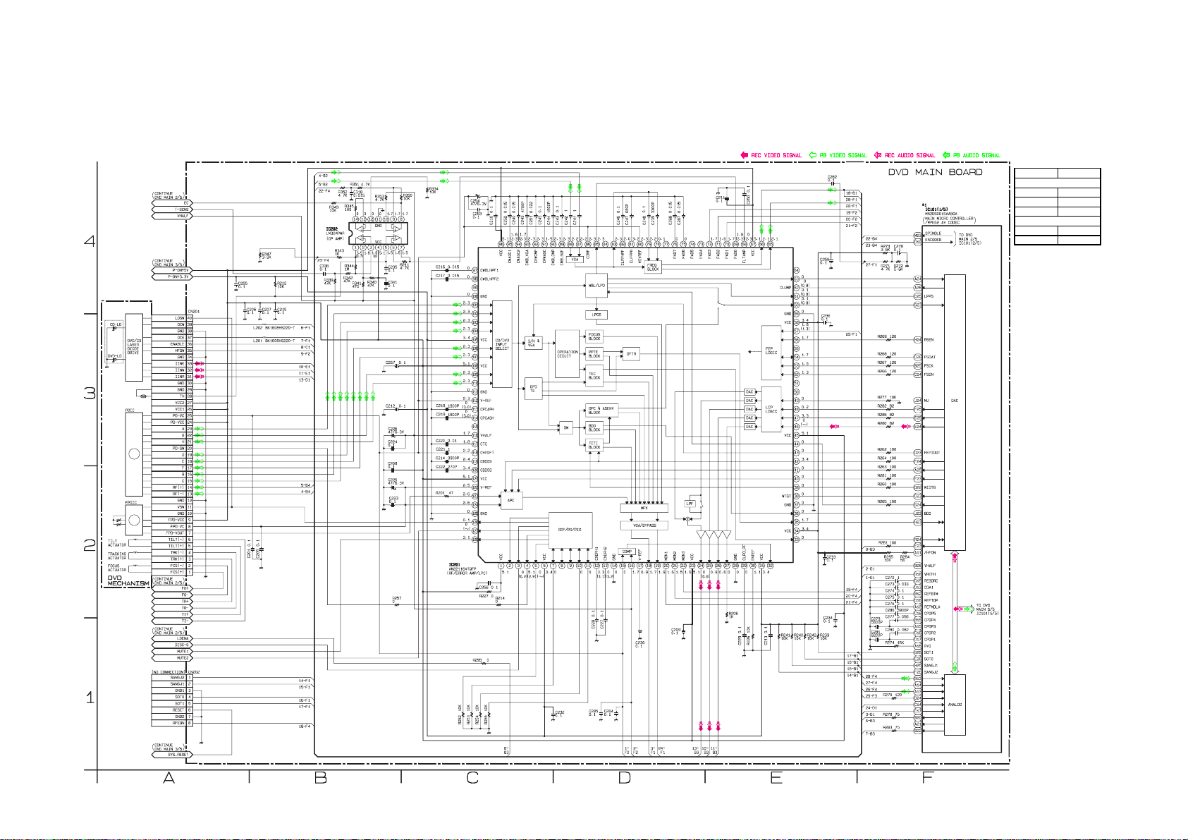
DVD Main 1/5 Schematic Diagram
NOTE:
1. The order of pins shown in this diagram is different from that of actual IC101.
2. IC101 is divided into five and shown as IC101 (1/5) ~ IC101 (5/5) in this DVD Main Schematic Diagram Section.
NOTE: BOARD MEANS PRINTED CIRCUIT BOARD.
DVD MAIN 1/5
Ref No. Position
ICS
IC101(1/5) F-4
IC201 C-2
IC202 B-4
CONNECTORS
CN201 A-3
CN202 A-1
1-11-3
E7A70SCD1
Page 10
DVD Main 2/5 Schematic Diagram
NOTE:
1. The order of pins shown in this diagram is different from that of actual IC101.
2. IC101 is divided into five and shown as IC101 (1/5) ~ IC101 (5/5) in this DVD Main Schematic Diagram Section.
NOTE: BOARD MEANS PRINTED CIRCUIT BOARD.
DVD MAIN 2/5
Ref No. Position
ICS
IC101(2/5) J-3
IC301 J-2
IC302 H-2
CONNECTORS
CN301 G-2
CN701 G-4
1-11-4
E7A70SCD2
Page 11

DVD Main 3/5 Schematic Diagram
DVD MAIN 3/5
Ref No. Position
IC101(3/5) N-4
IC106 P-2
IC107 P-2
CN101 R-3
ICS
CONNECTOR
NOTE:
1. The order of pins shown in this diagram is different from that of actual IC101.
2. IC101 is divided into five and shown as IC101 (1/5) ~ IC101 (5/5) in this DVD Main Schematic Diagram Section.
NOTE: BOARD MEANS PRINTED CIRCUIT BOARD.
1-11-5
E7A70SCD3
Page 12

DVD Main 4/5 Schematic Diagram
DVD MAIN 4/5
Ref No. Position
IC101(4/5) U-4
IC10 2 W- 4
IC104 S-4
ICS
NOTE:
1. The order of pins shown in this diagram is different from that of actual IC101.
2. IC101 is divided into five and shown as IC101 (1/5) ~ IC101 (5/5) in this DVD Main Schematic Diagram Section.
NOTE: BOARD MEANS PRINTED CIRCUIT BOARD.
1-11-6
E7A70SCD4
Page 13

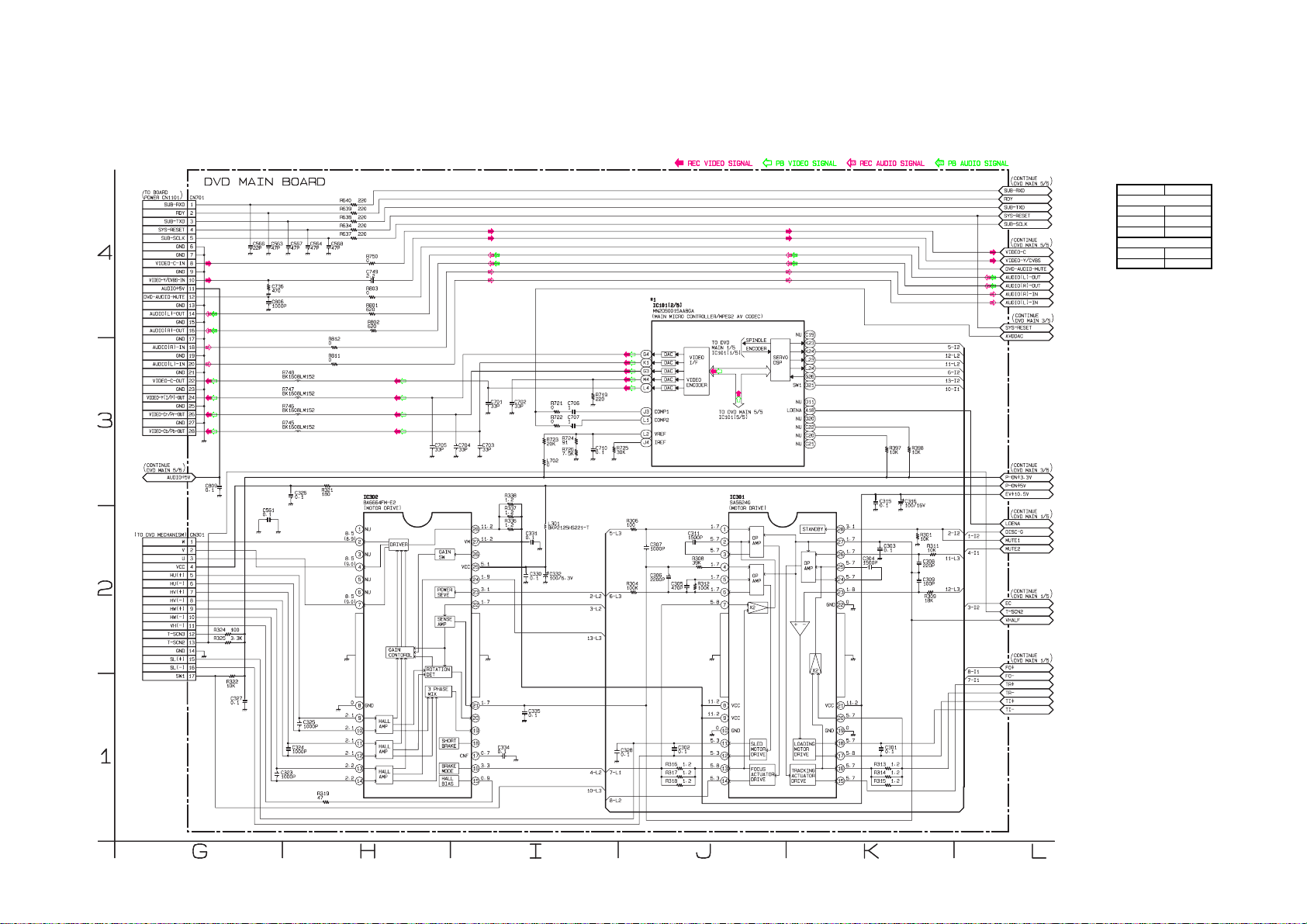
DVD Main 5/5 Schematic Diagram
DVD MAIN 5/5
Ref No. Position
IC101(5/5) Y-4
IC701 AA-2
IC801 CC-1
IC802 BB-1
ICS
NOTE:
1. The order of pins shown in this diagram is different from that of actual IC101.
2. IC101 is divided into five and shown as IC101 (1/5) ~ IC101 (5/5) in this DVD Main Schematic Diagram Section.
NOTE: BOARD MEANS PRINTED CIRCUIT BOARD.
1-11-7
E7A70SCD5
Page 14

POWER 1/5 Schematic Diagram
*1 NOTE
These components (IC1502A, C1509A, IC1502B, C1509B)
can be used in any models.
However, you cannot mix components under
Group A with the ones under Group B.
You can choose either Group. The difference
between Group A and Group B is shown below.
IC1502A
IC1502B
R3112N191A-TR-(FA,FB)
/BU4219G-TR
PST3619NR
Group A Group B
C1509A
C1509B
0.015
0.1
----------
----------
----------
----------
NOTE: BOARD MEANS PRINTED CIRCUIT BOARD.
POWER 1/5
Ref No. Position
ICS
IC1501 C-2
IC1502A D-1
IC1502B E-1
TRANSISTORS
Q1501 D-3
Q1502 E-3
CONNECTOR
CN1502 A-1
1-11-8
E7A70SCP1
Page 15

POWER 2/5 Schematic Diagram
POWER 2/5
Ref No. Position
IC1101 J-2
IC1102 J-1
IC1301 H-2
IC1701 J-4
Q1101 J-3
Q1102 J-3
Q1303 J-2
Q1304 J-1
CN1101 L-3
ICS
CONNECTOR
TRANSISTORS
NOTE: BOARD MEANS PRINTED CIRCUIT BOARD.
1-11-9
E7A70SCP2
Page 16

POWER 3/5 Schematic Diagram
POWER 3/5
Ref No. Position
IC1201 N-2
IC1401 O-3
Q1161 M-3
Q1201 P-2
Q1202 P-1
Q1203 O-2
Q1241 P-1
ICS
TRANSISTORS
NOTE: BOARD MEANS PRINTED CIRCUIT BOARD.
1-11-10
E7A70SCP3
Page 17

POWER 4/5 Schematic Diagram
POWER 4/5
Ref No. Position
IC1001 T-1
IC1503 V-4
IC1504 V-3
Q1001 T-2
Q1002 T-3
Q1003 S-1
Q1053 V-2
Q1054 V-2
Q1055 U-1
Q1056 V-1
Q1057 W-2
Q1063 W-1
Q1065 U-2
Q1151 W-1
Q1505 W-3
CN1051 X-4
ICS
CONNECTOR
TRANSISTORS
CAUTION !
Fixed voltage (or Auto voltage selectable) power supply circuit is used in this unit.
If Main Fuse (F1001) is blown , check to see that all components in the power supply
circuit are not defective before you connect the AC plug to the AC power supply.
Otherwise it may cause some components in the power supply circuit to fail.
F
A V
NOTE: BOARD MEANS PRINTED CIRCUIT BOARD.
CAUTION !
For continued protection against fire hazard,
replace only with the same type fuse.
ATTENTION : Pour une protection continue les risqes
d'Incele n'utiliser que des fusible de même type.
Risk of fire-replace fuse as marked.
"This symbol means fast operating fuse."
"Ce symbole reprèsente un fusible à fusion rapide."
NOTE:
The voltage for parts in hot circuit is measured using
hot GND as a common terminal.
1-11-11
E7A70SCP4
Page 18

POWER 5/5 Schematic Diagram
7G
REC
PM
REPEAT
g
6G
5G 4G 3G 2G 1G
VCD VCR
CD
T C
h
h
c
DVD
a
d
g
R
XP SP
b
LP EP
SLP
ef
P.SCAN
NOTE: BOARD MEANS PRINTED CIRCUIT BOARD.
W
SEP
FL2001 MATRIX CHART
7G 6G 5G 4G 3G 2G 1G
a
b
c
d
e
f
g
hh
i
ababababa
c
d
e
REC
f
PM
gg
REPEAT
VCD VCR DVD
CD
c
c
d
d
e
e
f
f
g
g
T
XP
b
c
d
e
f
g
C
SP
LP
EP
SLP
SEP
P.SCAN
W
R
c
d
e
f
g
1-11-12
E7A70SCP5
Page 19

SWITCH Schematic Diagram
NOTE: BOARD MEANS PRINTED CIRCUIT BOARD.
1-11-13
E7A70SCSW
Page 20

BOARD POWER Top View
CAUTION !
Fixed voltage (or Auto voltage selectable) power supply circuit is used in this unit.
If Main Fuse (F1001) is blown , check to see that all components in the power supply
circuit are not defective before you connect the AC plug to the AC power supply.
Otherwise it may cause some components in the power supply circuit to fail.
NOTE: BOARD MEANS PRINTED CIRCUIT BOARD.
CAUTION !
F
For continued protection against fire hazard,
replace only with the same type fuse.
A V
NOTE:
The voltage for parts in hot circuit is measured using
hot GND as a common terminal.
ATTENTION : Pour une protection continue les risqes
d'Incele n'utiliser que des fusible de même type.
Risk of fire-replace fuse as marked.
"This symbol means fast operating fuse."
"Ce symbole reprèsente un fusible à fusion rapide."
1-11-14 BE7A00F01022A
Page 21

"Ce symbole reprèsente un fusible à fusion rapide."
CAUTION !
For continued protection against fire hazard,
replace only with the same type fuse.
ATTENTION : Pour une protection continue les risqes
d'Incele n'utiliser que des fusible de même type.
Risk of fire-replace fuse as marked.
"This symbol means fast operating fuse."
A V
F
BOARD POWER
Ref No. Position
IC1001 D-2
IC1101 B-5
IC1102 A-5
IC1201 D-3
IC1301 D-1
IC1401 E-4
IC1501 A-3
IC1502 B-2
IC1503 C-3
IC1504 C-2
IC1701 C-5
IC2001 A-2
Q1001 D-2
Q1002 D-1
Q1003 D-2
Q1053 C-2
Q1054 B-2
Q1055 D-2
Q1056 B-2
Q1057 B-2
Q1063 B-2
Q1065 B-2
Q1101 A-4
Q1102 A-4
Q1151 B-2
Q1161 B-5
Q1201 E-3
Q1202 E-3
Q1203 D-3
Q1241 E-2
Q1303 D-4
Q1304 D-5
Q1501 B-2
Q1502 A-1
Q1505 B-1
CN1051 C-3
CN1101 B-3
CN1502 A-2
ICS
CONNECTORS
TRANSISTORS
BOARD POWER Bottom View
WF3
C1418
PLUS LEAD
WF7
PIN 28 OF
CN1051
CAUTION !
Fixed voltage (or Auto voltage selectable) power supply circuit is used in this unit.
If Main Fuse (F1001) is blown , check to see that all components in the power supply
circuit are not defective before you connect the AC plug to the AC power supply.
Otherwise it may cause some components in the power supply circuit to fail.
1-11-15
NOTE: BOARD MEANS PRINTED CIRCUIT BOARD.
NOTE:
The voltage for parts in hot circuit is measured using
hot GND as a common terminal.
WF4
PIN 28 OF
CN1101
WF5
PIN 26 OF
CN1101
WF1
PIN 24 OF
CN1101
WF2
PIN 22 OF
CN1101
WF6
PIN 14 OF
CN1101
BE7A00F01022A
Page 22

BOARD SWITCH Top View
BOARD SWITCH Bottom View
NOTE: BOARD MEANS PRINTED CIRCUIT BOARD.
BOARD SWITCH
BOARD SWITCH
1-11-16
BE7A00F01022B
Page 23

WF1
Pin 24 of CN1101
WAVEFORMS
WF5
Pin 26 of CN1101
VIDEO-Y 0.2V 20µsec
WF2
Pin 22 of CN1101
VIDEO-C 0.2V 20
WF3
C1418 PLUS LEAD
VIDEO-Cr
WF6
Pin 14 of CN1101
µ
sec
AUDIO(L)-OUT
WF7
Pin 28 of CN1051
0.2V 20µsec
1V 0.5ms
VIDEO-CVBS 0.5V 20
WF4
Pin 28 of CN1101
VIDEO-Cb
0.2V 20µsec
µ
µ
sec
SPDIF 1V 0.1
sec
NOTE:
Input: COLOR BAR SIGNAL
(WITH 1KHz AUDIO SIGNAL)
1-12-1
R3NWF
Page 24

DVD MECHANISM & DVD MAIN BOARD ASSEMBLY
NOTE: BOARD MEANS PRINTED CIRCUIT BOARD.
DVD MECHANISM
SLED
SENSOR
ENCODER
BOARD
SPINDLE
M
MOTOR
SLED
M
MOTOR
PICKUP
DVD-LD
CD-LD
FOCUS
ACTUATOR
TRACKING
ACTUATOR
TILT
ACTUATOR
FPDIC
PDIC
DVD/CD
LASER
DIODE
DRIVE
CN1003
1
2
3
RELAY
BOARD
CN1002
1
~
11
CN1001
SW1
SL(-)
SL(+)
GND
T-SCN2
T-SCN3
VH(-)
HW(+)
HV(+)
HU(-)
HU(+)
VCC
U
V
W
CN301
172
163
154
145
136
127
118
109 HW(-)
910
811 HV(-)
712
613
514
415
316
217
118
CN201
FCS(+)
1
2 FCS(-)
TRK(+)
3
TRK(-)
4
5 TILT(+)
6 TILT(-)
7 FPD-VOUT
FPD-VC
8
9 FPD-VCC
GND
10
FPD-VSW
11
GND
12
RF(-)
13
RF(+)
14
C
15
B
16
F
17
E
18
D
19
PD-SW
20
H
21
G
22
A
23
PD-VCC
24
PD-VC
25
VCC1
26
VCC2
27
TH
28
GND
29
GND
30
IINR
31
IINW
32
IINE
33
GND
34
HFSW
35
ENABLE
36
OCE
37
GND
38
OCW
39
LDSW
40
WIRING DIAGRAM
DVD MAIN BOARD
CN101
CN701
W2
GND 11
GND 22
GND 33
EV+10.5V 44
EV+10.5V 55
EV+10.5V 66
GND 77
GND 88
P-ON+5V 99
P-ON+5V 1010
P-ON+5V 1111
GND 1212
GND 1313
P-ON+3.3V 1414
P-ON+3.3V 1515
P-ON+3.3V 1616
GND 1717
GND 1818
VI+1.2V 1919
VI+1.2V 2020
VI+1.2V 2121
GND 2222
GND 2323
P-ON+2.5V(1) 2424
P-ON+2.5V(1) 2525
GND 2626
GND 2727
SPDIF 2828
GND 2929
1V2CONT 3030
W3
SUB-RXD 11
RDY 22
SUB-TXD 33
SYS-RESET 44
SUB-SCLK 55
GND 66
GND 77
VIDEO-C-IN 88
GND 99
VIDEO-Y/CVBS-IN
AUDIO+5V 1111
DVD-AUDIO-MUTE
GND 1313
AUDIO(L)-OUT
GND
AUDIO(R)-OUT
GND
AUDIO(R)-IN
GND 1919
AUDIO(L)-IN
GND
VIDEO-C-OUT 2222
GND 2323
VIDEO-Y(I/P)-OUT
GND 2525
VIDEO-Cr/Pr-OUT
GND
VIDEO-Cb/Pb-OUT
1010
1212
1414
1515
1616
1717
1818
2020
2121
2424
2626
2727
2828
CN1051
CN1101
BOARD POWER
W5
KEY-1 11
KEY-2 22
GND 33
S-VIDEO
IN1
S-VIDEO
OUT
VIDEO
-IN1
VIDEO
OUT
VIDEO-Y
OUT
VIDEO-Cb/Pb
OUT
VIDEO-Cr/Pr
OUT
AUDIO(L)
-IN1
AUDIO(R)
-IN1
AUDIO(L)
-OUT1
AUDIO(R)
-OUT1
DIGITAL
AUDIO OUT
(COAXIAL)
ANT-IN
ANT-OUT
S-VIDEO
IN2
VIDEO
-IN2
AUDIO(L)
-IN2
AUDIO(R)
-IN2
CN3001CN1502
BOARD SWITCH
REAR
FRONT
AC CORD
1-13-1
E7A70WI
Page 25

SYSTEM CONTROL TIMING CHARTS
Yes
No
Is Timer
ET1 passed?
Case 1
No
Power on
INNER-SW
open?
No
Rezero 1
INNER-SW
open?
Yes
To disc
distintion
Case 2
Yes
Rezero 2
[ Tray Open ]
button is pressed.
[ Tray Open ]
button is pressed.
Tray insertion
Is slit S5
passed?
Is Timer
ET4 passed?
INNER-SW
No
Case 3
[ open ] button is pressed.
No
Yes
Case 4
[ open ] button is pressed.
Yes
No
open?
Yes
Push Close
No
Is Timer
ET3 passed?
Yes
No
Tray ejection
Is slit S1
passed?
Yes
Is Timer
ET2 passed?
No
Is not
slit passed?
Yes
Tray ejection
completion
No
Yes
No
Is Timer
ET1 passed?
Yes
Case 5
Retry.
Yes
Retry OK?
In case of "No" by the 6th time retry.
No
Tray insertion
1-14-1 R2NTI
Page 26

Parameter
Tray o pen
V*: Voltage (HEX)
S*: Encoder pulse
(HEX)
T*: Event timer
ET*: Error
detection timer
V0: 2.0 V (00d) S1: 300 (12c) T1: 0.1 s ET1: 5.0 s
V1: 4.5 V (022) S2: 3300 (ce4) T2: 3.0 s ET2: 5.0 s
V2: 2.2 V (010) S3: 3935 (f5f) T3: 3.0 s ET3: 3.0 s
V3: 2.4 V (013) S4: 0 (000) T4: 0.1 s ET4: 3.0 s
V4: 6.0 V (030) S5: 3000 (bb8) T5: 0.1 s
Encoder pulse
S3
S2
S1
Tray ejection direction
Tray close
SLED
Tray insersion direction
open
INNER-SW
close
Timer ET1
Tray ejection direction
SLED
Tray insersion direction
S4
S5
ET2
T1
V0
V3
V2
V1
V4
INNER-SW
Timer
open
close
ET3 ET4
1-14-2 R2NTI
Page 27

Push close
Encoder pulse
S5
Push Close
SLED
Case 1
Tray insersion direction
open
INNER-SW
close
Timer
Tray insersion direction
INNER-SW
SLED
Timer
open
close
T2
T3
ET4
V3
V4
ET4
V3
V4
Case 2
Tray ejection direction
SLED
Tray insersion direction
open
INNER-SW
close
Rezero 1
V0V0
Rezero 2
1-14-3 R2NTI
Page 28

Case 3 (When [OPEN] button is pressed before the S5 passage.)
Encoder pulse
Tray ejection direction
SLED
V2
Timer
T1
Case 4 (When [OPEN] button is pressed after the S5 passage.)
It starts opening after making closing complete once.
Case 5 (Retry.)
S1
Tray ejection direction
SLED
Tray insersion direction
open
INNER-SW
V1+
V26v
close
Start retry.
Retry frequency V1+
1st time retry 6 v
2nd time retry 7 v
3rd time retry 8 v
4th time retry 9 v
5th time retry 9 v
6th time retry 9 v
1-14-4 R2NTI
Page 29

IC PIN FUNCTION DESCRIPTIONS
IC1501 (SUB MICRO CONTROLLER)
Pin
IN/
No.
OUT
1 IN KEY-1 Key Data Input 1
2 IN KEY-2 Key Data Input 2
3 IN POW-SW Abnormal Voltage Detection
4 IN AFT Tuner Voltage Input Signal
5 - NU Not Used
6 IN EV+3.3V +3.3V Power Supply
7 IN VCC +3.3V Power Supply
8 OUT XOUT Main Clock Output
9 IN XIN Main Clock Input
10 - GND Ground
11 IN XCIN Sub Clock Input
12 OUT XCOUT Sub Clock Output
13 - GND Ground
14 IN RESET
15 - NU Not Used
16 - NU Not Used
17 - NU Not Used
18 OUT SUB-TXD
19 IN SUB-RXD
20 OUT SUB-SCLK
21 - NU Not Used
22 OUT
23 - NU Not Used
24 - NU Not Used
25 - NU Not Used
26 OUT 1V2CONT
27 IN REMOTE Remote Signal Input
28 - NU Not Used
29 IN RDY
30 IN P-DOWN
31 - NU Not Used
32 - NU Not Used
IN/
33
OUT
34 OUT SCL Serial Clock
35 - NU Not Used
Signal
Name
Micro Controller Reset
Signal
Transmission Data to Main
Micro Controller
Reception Data from Main
Micro Controller
Communication Clock with
Main Micro Controller
SYSRESET
SDA Serial Data
System Reset Signal
Power Regulator Control
Signal
Ready/Busy communication
Control with Main Micro
Controller
Power Voltage Down
Detector Signal
Function
Pin
IN/
No.
OUT
36 - NU Not Used
37 - NU Not Used
38 OUT
39 OUT
40 OUT
41 OUT
42 OUT
43 OUT
44 OUT
45 - NU Not Used
46 - NU Not Used
47 - NU Not Used
48 OUT FL-SDA Serial Data
49 OUT FL-STB Serial Interface Strobe
50 OUT FL-SCL Serial Clock
51 - NU Not Used
52 OUT
53 OUT PWSW Power ON Signal Output
54 - NU Not Used
55 - NU Not Used
56 - NU Not Used
57 - NU Not Used
58 - NU Not Used
59 - NU Not Used
60 - NU Not Used
61 - GND Ground
62 - NU Not Used
63 - NU Not Used
64 - NU Not Used
Signal
Name
AUDIOMUTE
AUDIOSW2
AUDIOSW1
VIDEOSW1
VIDEOSW2
VIDEOSW3
VIDEOMUTE
REGCONT
Function
Audio Mute Control Signal
Audio Input Select Signal
Audio Input Select Signal
Video Input Select Signal
Video Input Select Signal
Video Input Select Signal
Video Mute Control Signal
Power Regulator Control
Signal
1-15-1 E7A70PIN
Page 30

IC2001 (VFD DRIVER)
Pin
IN/
No.
OUT
1 IN CLK Serial Clock
2 IN STB Serial Interface Strobe
3 - NU Not Used
4 - NU Not Used
5 - VSS GND
6 - VDD Power Supply
7
8 b
9 c
10 d
OUT
11 e
12 f
13 g
14 h
15 - VEE Pull Down Level
16 OUT i Segment Output
17
18 6G
19 5G
20 4G
OUT
21 3G
22 2G
23 1G
24 - VDD Power Supply
25 - VSS GND
26 IN OSC Oscillator Input
27 - NU Not Used
28 IN DIN Serial Data Input
Signal
Name
a
7G
Function
Segment Output
Grid Output
1-15-2 E7A70PIN
Page 31

LEAD IDENTIFICATIONS
KTC3203-Y-AT/P KTA1267Y-AT/P
E C B E C B
MM1697AJBE
24
1
13
12
KTA1271-Y-AT/P
KTC3199-GR-AT/P
KRC103M-AT/P
PT6313-S-TP(L)
28
1
15
14
UTC4558
8 5
1 4
PQ070XF01SZH
1234
2SK3757(Q)
GDS
MN101C77A FK2
48
49
64
1
1
2
1: Anode
4
2: Cathode
3
3: Emitter
4: Collector
33
16
32
17
MM1637XVBE
16
1
CD4052BNSR
16
1
9
8
9
8
AN5832SA-E1V
32
1
R3112N191A-TR-FA
PST3619NR
54
123
RC4580IPPS2561A-1(Q)
17
16
8
1
S2Y52(FUNAI Q H)BU4219G-TR
5
4
E C B
Note:
A: Anode
K: Cathode
E: Emitter
C: Collector
B: Base
R: Reference
G: Gate
D: Drain
S: Source
1-16-1 E7A70LE
 Loading...