

Quad FET Driver
UCC1776
UCC2776
UCC3776
PRELIMINARY
FEATURES
• High Peak Output Current
Each Output – 1.5A Source,
2.0A Sink
• Wide Operating Voltage
Range 4.5V to 18V
• Thermal Shutdown
• CMOS Compatible Inputs
• Outputs Are Active Low
for Undervoltage Lockout
Condition
DESCRIPTION
The UCC3776 is a four output BCDMOS buffer/driver designed to drive highly
capacitive loads such as power MOSFET gates at high speeds. The device
can be configured as either an inverting or non-inverting driver via the POL
pin.The outputs are enabled by ENBL.When disabled, all outputs are active
low. The device incorporates thermal shutdown with hysteresis for stability.
The device also includes an undervoltage lockout circuit (UVLO) with hysteresis which disables the outputs when VDD is below a preset threshold. The
outputs are held low during undervoltage lockout, even in the absence of
VDD power to the device.This helps prevent MOSFET turn-on due to capacitive current through the gate-drain capacitance of the power MOSFET in the
presence of high dV/dts. The logic input thresholds are compatible with
standard 5V HCMOS logic.
3/97
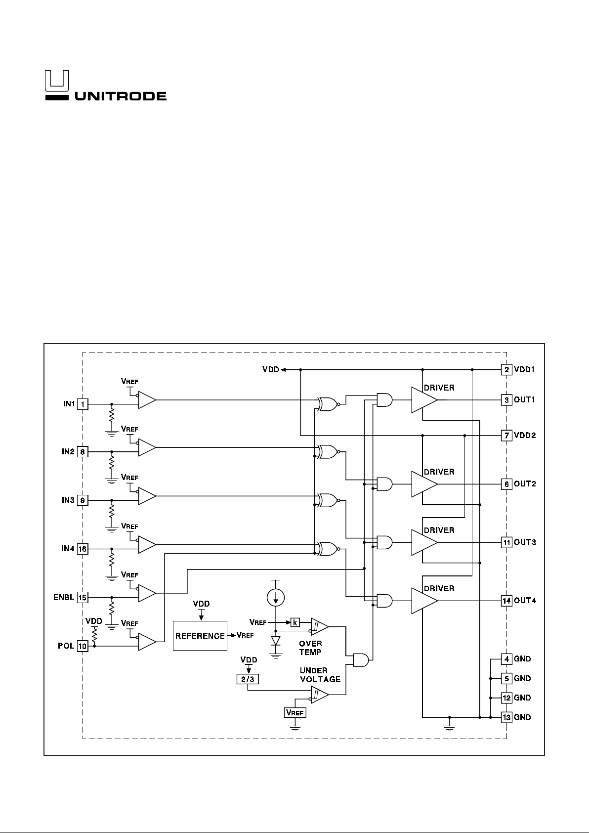
BLOCK DIAGRAM
UDG-95129-2
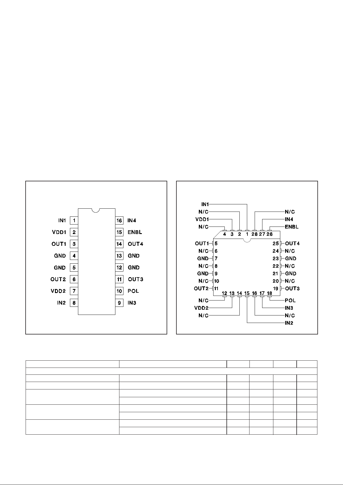
Note:Pin connections shown refer to 16-pin packages.
1
2
UCC1776
UCC2776
UCC3776
ABSOLUTE MAXIMUM RATINGS
Input Supply Voltage, VDD1, VDD2 . . . . . . . . . . . . . . . . . . . . . . . . . . . . . . . . . . . . .20V
Maximum DC Voltage Difference, VDD1 vs.VDD2 . . . . . . . . . . . . . . . . . . . . . . .100mV
Logic Input, IN1, IN4, ENBL
Maximum forced voltage . . . . . . . . . . . . . . . . . . . . . . . . . . . . . .−0.3 to VDD1 + 0.3V
Logic Inputs, IN2, IN3, POL
Maximum forced voltage . . . . . . . . . . . . . . . . . . . . . . . . . . . . . .−0.3 to VDD2 + 0.3V
Latch-up Protection withstand Reverse Current
IREV, OUT1, OUT2, OUT3, OUT4 . . . . . . . . . . . . . . . . . . . . . . . . . . . . . . . . .500mA
Power Outputs, OUT1, OUT2, OUT3, OUT4
Maximum pulsed current (10% duty max, 10µsec max pulse width) . . . . . . . . . .3A
Storage Temperature . . . . . . . . . . . . . . . . . . . . . . . . . . . . . . . . . . . . . .−65°C to +150°C
Operating Junction Temperature . . . . . . . . . . . . . . . . . . . . . . . . . . . . .−55°C to +150°C
Lead Temperature (Soldering, 10 Seconds) . . . . . . . . . . . . . . . . . . . . . . . . . . . . .300°C
All currents are positive into, negative out of the specified terminal.Consult Packaging
Section of Databook for thermal limitations and considerations of packages.
CONNECTION DIAGRAMS
DIL-16 (Top View)
N or J,DP Packages
PLCC-28 (Top View)
Q Package
ELECTRICAL CHARACTERISTICS Unless otherwise stated these specifications apply for TA = −55°C to +125°C for
UCC1776;−40°C to +85°C for UCC2776;0°C to +70°C for UCC3776;VPOL = 5V, VENBL = 5V, 4.5V <VDD < 18V, TJ = TA.
PARAMETER TEST CONDITIONS MIN TYP MAX UNITS
Input Section
VIH, Logic 1 Input Voltage 3 V
VIL, Logic 0 Input Voltage 2 V
IINn, Input Current VINn = 5V 30 µA
VINn = 0V –1 +1 µA
ENBL Input Current VENBL = 5V 30 µA
VENBL = 0V –1 +1 µA
POL Input Current VPOL = 5V −1 +1 µA
V
POL = 0V −30 µA
3
UCC1776
UCC2776
UCC3776
Note 1:Guaranteed by design.Not 100% tested in production.
ELECTRICAL CHARACTERISTICS (cont.) Unless otherwise stated these specifications apply for TA = −55°C to +125°C
for UCC1776;−40°C to +85°C for UCC2776;0°C to +70°C for UCC3776;VPOL = 5V, VENBL = 5V, 4.5V <VDD < 18V, TJ = TA.
PARAMETERTEST CONDITIONS MIN TYP MAX UNITS
Output Section
VOH, High Output Voltage IOUTn = -10mA, VDD1 = VDD2= 12V, VINn = 5V VDD− 1.0 V
VOL, Low Output Voltage IOUTn = 10mA, VDD1 = VDD2 = 12V, VINn = 0V 0.15 V
Output Resistance IOUTn = 10mA, VDD1 = VDD2 = 12V, VINn = 0V 6 Ω
Output High Peak Current VDD1 = VDD2 = 12V, OUTn = 5V, V
INn = 5V, −1.5 A
TJ = 25°C (Note 1)
Output Low Peak Current VDD1 = VDD2 = 12V, OUTn = 5V, V
INn = 0V, 2.0 A
TJ = 25°C (Note 1)
UVLO Output Pull-down Voltage VDD1 = VDD2 = 3V, IOUTn = −10mA 0.8 1.5 V
Switching Time Section
Output Rise Time C
OUTn = 1nF, VOUTn = 1V to 9V,
VDD1 = VDD2 = 12V 25 50 nsec
Output Fall Time C
OUTn = 1nF, VOUTn = 9V to 1V,
VDD1 = VDD2 = 12V 10 50 nsec
IN−>OUT Delay Time (Rising Output) V
INn = 2.5V, VOUTn = 0.1 • VDD, 40 100 nsec
VDD1 = VDD2 = 12, COUTn = 0nF
IN−>OUT Delay Time (Falling Output) V
INn = 2.5V, VOUTn = 0.9 • VDD, 50 100 nsec
VDD1 = VDD2 = 12V, COUTn = 0nF
Power Supply Section
Power Supply Current V(IN1−IN4) = 0V, V
ENBL = 0V, 2 mA
VDD1 = VDD2 = 12V
UVLO Threshold 4.5 V
UVLO Hysteresis 0.5 V
ENBL: Logic level input to enable the drivers.When ENBL
is low, the drivers outputs will be at GND potential, regardless of the status of POL.The input threshold is designed
to be 5 volt CMOS compatible, independent of the VDD
voltage used on the device.There is a slight hysteresis in
the input circuit to help reduce sensitivity to noise on the
input signal or input ground.
GND: Ground for the device, the supply return for the
VDDs. There are four GND pads on the device.
IN1 - IN4: Inputs to each driver (1-4).The input threshold
is designed to be 5 volt CMOS compatible, independent
of the VDD voltage used on the device.There is a slight
hysteresis in the input circuit to help reduce sensitivity
to noise.
OUT1 - OUT4: Outputs to each driver (1-4). The outputs
are totem pole DMOS circuits. In the absence of VDD on
the device, the outputs will stay off, even with a capacitive
displacement current into the output node.
POL: Polarity selection for the drivers. A logic 0 selects
inverting operation. A logic 1 selects non-inverting operation. The input threshold is designed to be 5 volt CMOS
compatible, independent of the VDD voltage used on the
device.There is a slight hysteresis in the input circuit to
help reduce sensitivity to noise.
VDD1: Supply Voltage for drivers 1 and 4. Tied inter nally
to VDD2.
VDD2: Supply Voltage for drivers 2 and 3.Tied internally
to VDD1.
PIN DESCRIPTIONS
APPLICATION INFORMATION
Figure 1 depicts a block diagram of the UCC3776 Quad
FET Driver. Four high current, high speed gate drivers
with CMOS compatible input stages are provided.
Polar ity select and enable inputs provide circuit integra-
tion flexibility, while power packaging and high speed
drive circuitry allow for driving high power MOSFET
gates in high speed applications.

4
UCC1776
UCC2776
UCC3776
APPLICATION INFORMATION (cont.)
Input Stage
Each of the four UCC3776 FET driver circuits provides
an independent, CMOS compatible input stage. The
allowable input voltage range extends from ground to
VDD, allowing for easy interface to a wide variety of
PWM and power supply support circuitry. The POL and
ENBL inputs are tied to all four drivers, and all drivers
must be configured as either inverting or noninverting,
and all must be either enabled or not enabled.
To prevent oscillations in noisy PWM environments, any
unused drivers should have their input stages tied to
either VDD or ground. Unlike other CMOS FET drivers,
quiescent power current is not significantly affected by
the polarity of the driver input signal.
Output Stage/Gate Driver Considerations
Many power FET driver data sheets rely solely on rise
and fall time specifications into a capacitive load to quan-
tify speed performance. While these specifications are
important, they do not provide all the required information. The UCC3776 specifies rise and fall times of 25ns
and 10ns respectively into a load of 1nF.This specification can be used to calculate the average slew rate capability of the driver stage over the output voltage range.
However, the gate of a power MOSFET cannot be modeled accurately with a simple capacitor. The voltage/current requirements of the gate vary widely over several
distinct phases of FET turn-on and turn-off. The most
accurate way to calculate the switching times of power
MOSFETs is to determine the total gate charge requirement (Qg), which is usually specified by the MOSFET
manufacturer, and determine the peak current capability
of the MOSFET gate driver.Ideally the dr iver’s peak current can be delivered while the MOSFET gate is transitioning through its plateau or “Miller” level, when current
demands are highest.
Figure 1.Typical FET Driver Application
UDG-96006

5
UCC1776
UCC2776
UCC3776
APPLICATION INFORMATION (cont.)
The UCC3776 specifies peak source and sink currents
for a driver output voltage of 5V. This output voltage
approximately coincides with the average gate plateau
voltage of a power MOSFET. Outside of the plateau
region the gate drive waveform is primarily limited by the
slew rate capability of the driver.Through proper analysis
of the MOSFET’s gate drive requirements and the specifications for the UCC3776, an accurate model of AC performance can be created. For a detailed description of
MOSFET AC gate drive requirements please see
Unitrode Application Notes U-118 and U-137. Although
the Unitrode power drivers referenced in these application notes are bipolar devices, the information relating to
MOSFET gate drive characteristics is applicable.
Power Supply Decoupling/Grounding
The high peak currents required to charge high capacitance MOSFET gates make proper power supply decoupling and grounding essential. The UCC3776 provides
two power supply inputs (VDD1 and VDD2) to allow for
optimum internal circuit layout and minimum resistive
voltage drop with high peak current loads. VDD1 provides the drive current for outputs 1 and 4, while VDD2
provides drive current for outputs 2 and 3.Both of these
pins must be externally connected to the source power
supply, and the DC potential difference between these
two points should be limited to 100mV. Under no circumstances should an output driver be used with only one
supply input connected.
To guarantee a low impedance current path over a wide
frequency range, each supply input should be separately
bypassed to ground with both a high value tantalum or
electrolytic capacitor in parallel with a 0.1µF ceramic
capacitor. The exact value of the tantalum or electrolytic
capacitor will depend on the charge requirements of the
MOSFET gate. For most applications a value between
1µF and 10µF should suffice. Connections for ground
leads should be kept as short as possible. The driver
chip and support electronics should be located over a
large copper ground plane if layout conditions allow it.
Power Dissipation/Thermal Considerations
Being a CMOS device, the standby power dissipation of
the UCC3776 is quite low. For a 15V supply, the maximum quiescent current of 2mA results in a maximum
power loss of only 30mW. However, driving high frequency MOSFETs at high peak currents results in additional
power dissipation.This is because each time the MOSFET gate is charged or discharged, the energy transfer is
only 50% efficient. The same amount of energy that is
transferred to the gate is lost in the drive stage.
In order to determine the average output stage loss, the
gate drive energy (WGD) is computed as:
1) WGD = 2 • 0.5 • CG • V2= • V2= QG • V
Where QG is the MOSFET’s total gate charge, and V is
the gate voltage. The factor of two results from the fact
that the gate drive circuit must charge and discharge the
gate every electrical cycle.Each time the gate is charged
or discharged, the gate drive dissipates an amount of
energy equal to the energy supplied to the gate. Power
lost due to driving the gate is:
2) PLGD = = = QG • V • F
Where F is the operating frequency of the MOSFET.This
is a worst case assumption since the power loss is
shared by the output driver and the gate resistor.If a relatively large value series gate resistor is used, the power
loss in the gate driver is reduced.The penalty for this is
slower switching speed, and therefore more loss in the
MOSFET. For high power MOSFETs this power loss can
be significant.
To illustrate a typical example of driver loss, consider a
MOSFET with 70nC of gate charge and a 15V gate voltage. The power loss at 200kHz is:
3) PLGD = 70nC • 15V • 200kHz = 210mW
This analysis applies to one of the four drivers on the
UCC3776. Four drivers operating under the same conditions results in a total power loss of 840mW. At higher
frequencies the dissipation will be proportionally greater.
This example demonstrates the need for power packaging which is available on the UCC3776, and not available
on many other FET drivers.
After device power dissipation has been estimated, proper heat sinking must be provided to ensure that the
device junction temperature does not exceed the specified maximum. Refer to the packaging section of the
databook for package thermal impedance information.
Application Circuits
Figure 1 depicts a typical gate drive application circuit.
Four independent, noninverting low side FET drivers are
shown. Although series gate drive resistors are not
required because all FET drivers have a finite peak current
capability, it is good practice to include some series resistance to limit peak current and to prevent oscillations due
to parasitic inductance and capacitance.The parallel diode
and resistor allow for a faster gate turn off than turn on.
This characteristic is often desirable for bridge driver applications to prevent MOSFET cross conduction in the power
stage.
Q • V
T
WGD
T
QG
V
Figure 2 shows an applications circuit with paralleled output drivers. If it is required to drive high gate charge
MOSFETs, the UCC3776 output drivers can be combined
for higher peak current capability.It is good practice to provide separate gate resistor networks to each individual
MOSFET as shown.This will ensure that each driver circuit will not see excessive current during the high gate
charge portion of the switching waveform. This practice
also tends to isolate driver circuits to reduce the possibility
of ringing and crosstalk.If all four drivers are used to drive
a single MOSFET, then four separate gate drive resistor
networks should be used.
Figure 3 shows a transformer coupled full bridge power
stage. The UCC3776 is ideally suited for interfacing
between low power PWM outputs and high power output
stages. Although the UC3879 phase shift controller is
shown in this example, the UCC3776 can be used in
many PWM controller applications where high power FET
drivers are required.
6
UCC1776
UCC2776
UCC3776
Figure 2.Parallel Output Drivers
APPLICATION INFORMATION (cont.)
UDG-96007
Figure 3.Full Bridge Driver Application
UDG-96008-1
UNITRODECORPORATION
7 CONTINENTAL BLVD.• MERRIMACK, NH 03054
TEL.(603) 424-2410 • FAX (603) 424-3460

IMPORTANT NOTICE
T exas Instruments and its subsidiaries (TI) reserve the right to make changes to their products or to discontinue
any product or service without notice, and advise customers to obtain the latest version of relevant information
to verify, before placing orders, that information being relied on is current and complete. All products are sold
subject to the terms and conditions of sale supplied at the time of order acknowledgement, including those
pertaining to warranty, patent infringement, and limitation of liability.
TI warrants performance of its semiconductor products to the specifications applicable at the time of sale in
accordance with TI’s standard warranty. Testing and other quality control techniques are utilized to the extent
TI deems necessary to support this warranty. Specific testing of all parameters of each device is not necessarily
performed, except those mandated by government requirements.
CERT AIN APPLICATIONS USING SEMICONDUCTOR PRODUCTS MAY INVOLVE POTENTIAL RISKS OF
DEATH, PERSONAL INJURY, OR SEVERE PROPERTY OR ENVIRONMENTAL DAMAGE (“CRITICAL
APPLICATIONS”). TI SEMICONDUCTOR PRODUCTS ARE NOT DESIGNED, AUTHORIZED, OR
WARRANTED TO BE SUITABLE FOR USE IN LIFE-SUPPORT DEVICES OR SYSTEMS OR OTHER
CRITICAL APPLICATIONS. INCLUSION OF TI PRODUCTS IN SUCH APPLICA TIONS IS UNDERSTOOD T O
BE FULLY AT THE CUSTOMER’S RISK.
In order to minimize risks associated with the customer’s applications, adequate design and operating
safeguards must be provided by the customer to minimize inherent or procedural hazards.
TI assumes no liability for applications assistance or customer product design. TI does not warrant or represent
that any license, either express or implied, is granted under any patent right, copyright, mask work right, or other
intellectual property right of TI covering or relating to any combination, machine, or process in which such
semiconductor products or services might be or are used. TI’s publication of information regarding any third
party’s products or services does not constitute TI’s approval, warranty or endorsement thereof.
Copyright 1999, Texas Instruments Incorporated
 Loading...