UCC2751
UCC3751
PRELIMINARY
DESCRIPTION
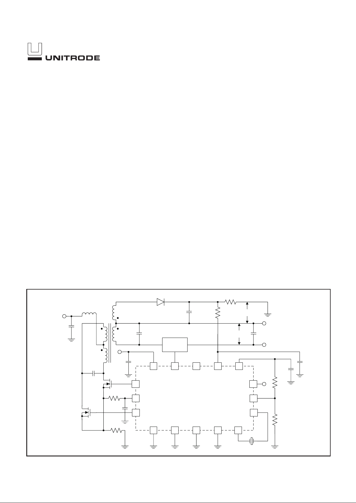
The UCC3751 controller is designed for driving a power stage that gener
ates low frequency, high voltage sinusoidal signals for telephone ringing
applications. The controller and the power stage are most suitable for sin
gle line applications where low cost, high efficiency and minimum parts
count are critical. In addition to providing the sinusoidal ringing signal, the
controller and the power stage are designed to provide the required DC
voltage across the output when the phone goes off-hook. The DC voltage
is also added as the offset to the ringing signal. This feature eliminates the
need to have a separate talk battery voltage power supply as well as relays
and drivers to switch between the ringing voltage and the talk battery.
The UCC3751 directly drives primary side switches used to implement a
push-pull resonant converter topology and transformer coupled sampling
switches located on the secondary of the converter. For normal ring signal
generation, the primary switching frequency and secondary sampling fre
quency are precisely offset from each other by the ringing frequency to pro
duce a high voltage low frequency alias signal at the output. The off-hook
condition is detected by sensing the AC current and when AC limit is exceeded, the sampling frequency is set to be equal to the primary switching
frequency to produce a DC output.
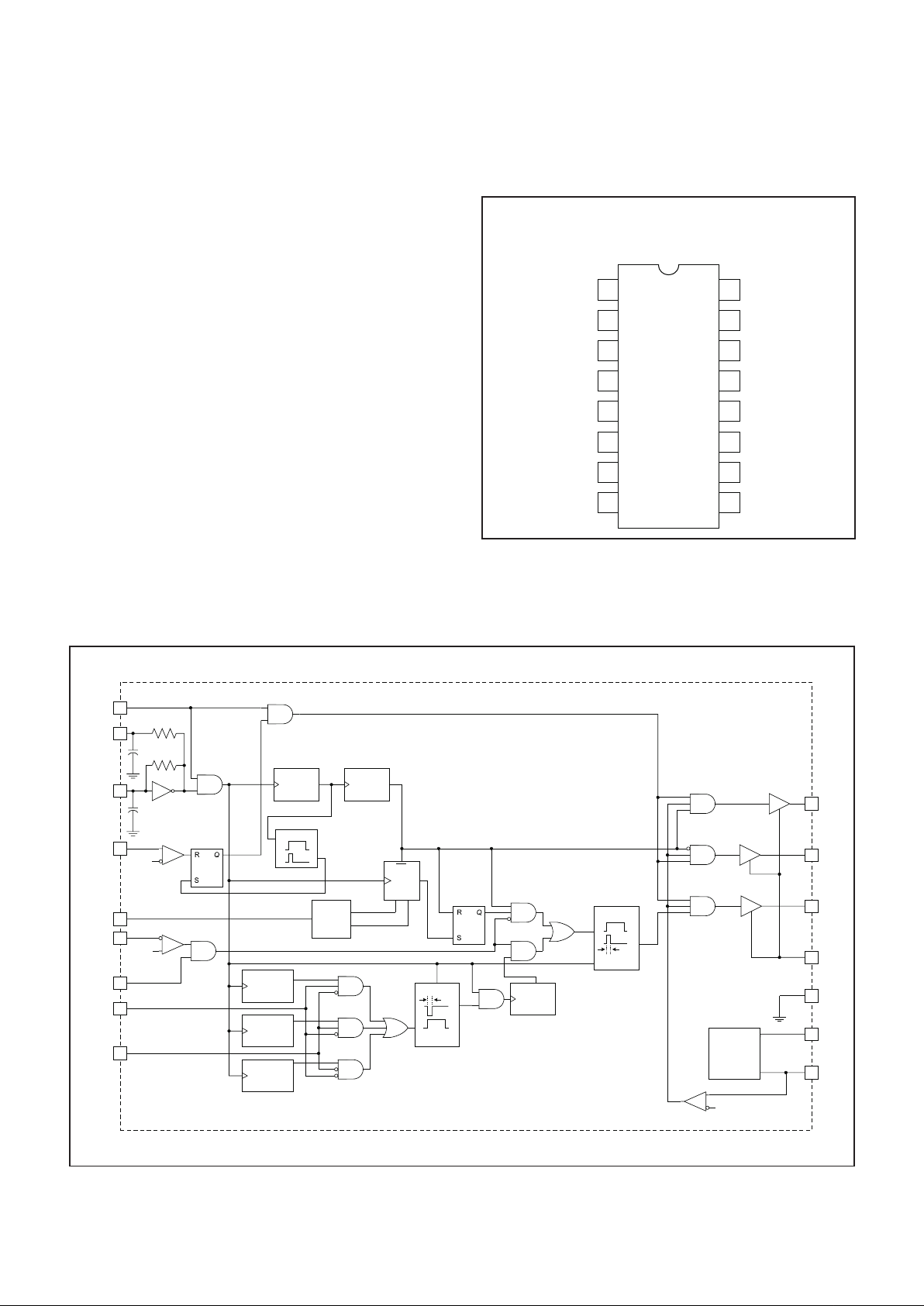
The drive signal frequencies are derived from a high frequency (3579545
Hz) crystal. The primary switching frequency is 89.488 kHz and the sampling frequency is 20, 25 or 50 Hz less depending on the status of frequency select pins FS0 and FS1.
Single Line Ring Generator Controller
FEATURES
•
Novel Topology for Low-Cost, Efficient
Generation of Ring Voltage
•
Provides DC Offset and “Talk Battery”
Voltage for Off-Hook Conditions
•
Selectable 20, 25 and 50 Hz Ring
Frequency
•
Secondary (AC) Current Limiting
Allows Removal of AC Voltage under
Off-Hook Conditions
•
Primary Current Limiting to turn Power
Stage off under Fault Conditions
•
Operates from a Single 12V Supply
SLUS267A - JULY 1999
1
10
15
4
ENABLE
VDD
DELAY
XTAL2
6
OHD
2
RINGEN
12
DRVS
9
VS12
5
11
13
DRV1
DCLIM
DRV2
16
XTAL1
8
FS1
7
FS0
14
PGND
3
GND
C
BYP2
SAMPLING
CIRCUIT
C
F
AC SIGNAL
V
OUT
V
1
C
R2
12V
C
DC
D1
DC SIGNAL
Q1
L
IN
V
IN
12V
T1
L
R
L
R
N:1
Q2
R
SENSE
UCC3751
3.579545MHz
C
R1
C
BYP1
TYPICAL APPLICATIONS CIRCUIT
UDG-98047
The circuits described in this datasheet are covered under US Patent #5,663,878 and other patents pending.

2
UCC2751
UCC3751
DIL-16, SOIC-16 (TOP VIEW)
N or D Packages
ABSOLUTE MAXIMUM RATINGS
Input Supply Voltage . . . . . . . . . . . . . . . . . . . . . . . . . . . . . 14V
Analog Inputs (OHD, DCLIM, XTAL1, XTAL2)
Maximum Forced Voltage. . . . . . . . . . . . . . . . . . . . –0.3 to 5V
Logic Inputs
Maximum Forced Voltage . . . . . . . . . . . . . . . . . . –0.3 to 7.5V
Reference Output Current (V
DD
)
. . . . . . . . . . . Internally Limited
Output Current (DRV1, DRV2, DRVS) Pulsed. . . . . . . . . . 1.5A
Operating Junction Temperature . . . . . . . . . . –55°C to +125°C
Storage Temperature . . . . . . . . . . . . . . . . . . . –65°C to +150°C
Note: Unless otherwise indicated, voltages are referenced to
ground and currents are positive into, negative out of, the spe
-
cific terminals. Pulsed is defined as a less than 10% duty cycle
with a maximum duration of 500
µ
S.
PGND
XTAL2
XTAL1
DRV2
DRVS
ENABLE
DRV1
VS12
1
2
3
4
5
6
7
8
16
15
14
13
12
11
10
9
RINGEN
DELAY
FS1
OHD
FS0
GND
V
DD
DCLIM
CONNECTION DIAGRAM
11
4
13
OHD
DRV1
RINGEN
14
9
3
12
DELAY
FS0
FS1
2
6
1
DRVS
VDD
GND
VS12
7
8
DRV2
PGND
5VOLT
REFERENCE
ONE-SHOT
1/F
OSC
4.5V
CLR
CLK
PROGRAMMABLE
COUNTER
MODULO
40
COUNTER
MODULO
3,560
COUNTER
MODULO
1,800
COUNTER
MODULO
4,480
COUNTER
2/FOSC
ONE-SHOT
2BIT
A/D
300mV
DCLIM 5
300mV
XTAL1 16
XTAL2 15
10
MODULO
2
COUNTER
ENABLE
MODULO
20
COUNTER
ONE-SHOT
BLOCK DIAGRAM
UDG-98020

3
UCC2751
UCC3751
ELECTRICAL CHARACTERISTICS:
Unless otherwise stated, these specifications hold for TA= 0°C to 70°C for the
UCC3751 and –40°C to +85°C for the UCC2751, TA=TJ.
PARAMETER TEST CONDITIONS MIN TYP MAX UNITS
V12 Supply Current Section
Supply Current ENABLE = 0V 0.5 3.0 mA
ENABLE = 5V 0.5 3.0 mA
Internal Reference with External Bypass Section
Output Voltage (VDD) 4.85 5 5.15 V
Load Regulation 0mA ≤ IV
DD
≤ 2mA 5 mV
Line Regulation 10V < VS12 < 13V, I
VDD
= 1mA 3 mV
Short Circuit Current V
DD
= 0 5 10 mA
Output Drivers Section (DRV1, DRV2)
Pull Up Resistance I
LOAD
= 10mA to 20mA 6 15 Ω
Pull Down Resistance I
LOAD
= 10mA to 20mA 6 15 Ω
Rise Time C
LOAD
= 1nF 50 100 nS
Fall Time C
LOAD
= 1nF 50 100 nS
Output Drivers Section (DRVS)
Pull Up Resistance I
LOAD
= 10mA to 20mA 4 10 Ω
Pull Down Resistance I
LOAD
= 10mA to 20mA 4 10 Ω
Sample Pulse-Width Mode 1 and 2, (Note 1) 280 nS
Rise Time C
LOAD
= 1nF 50 100 nS
Fall Time C
LOAD
= 1nF 50 100 nS
Current Limit Section
OHD Threshold 300 mV
OHD Input Current V
OHD
= 0V –100 nA
DCLIM Threshold 300 mV
DCLIM Input Current V
DCLIM
= 0V –100 nA
Frequency Section (Note 1)
Primary Switching Frequency All cases 3.579545 MHz Crystal 89489 Hz
Sampling Switching Frequency FS0 = 0, FS1 = 0, Mode 1, (Note 1) 89469 Hz
FS0 = 1, FS1 = 0, Mode 1 89464 Hz
FS0 = 0, FS1 = 1, Mode 1 89439 Hz
RINGEN OHD FS1 FS0 F
DRVS
F
DRV
–
F
DRVS
1 0 0 0 89.469kHz 20Hz
1 0 0 1 89.464kHz 25Hz
1 0 1 0 89.439kHz 50Hz
0 X X X 89.489kHz 0.0Hz
X 1 X X 89.489kHz 0.0Hz
FS1 FS0 MODE Sine Wave
Frequency (Hz)
001 20
011 25
101 50
113 0
OHD = 0.5 2 0
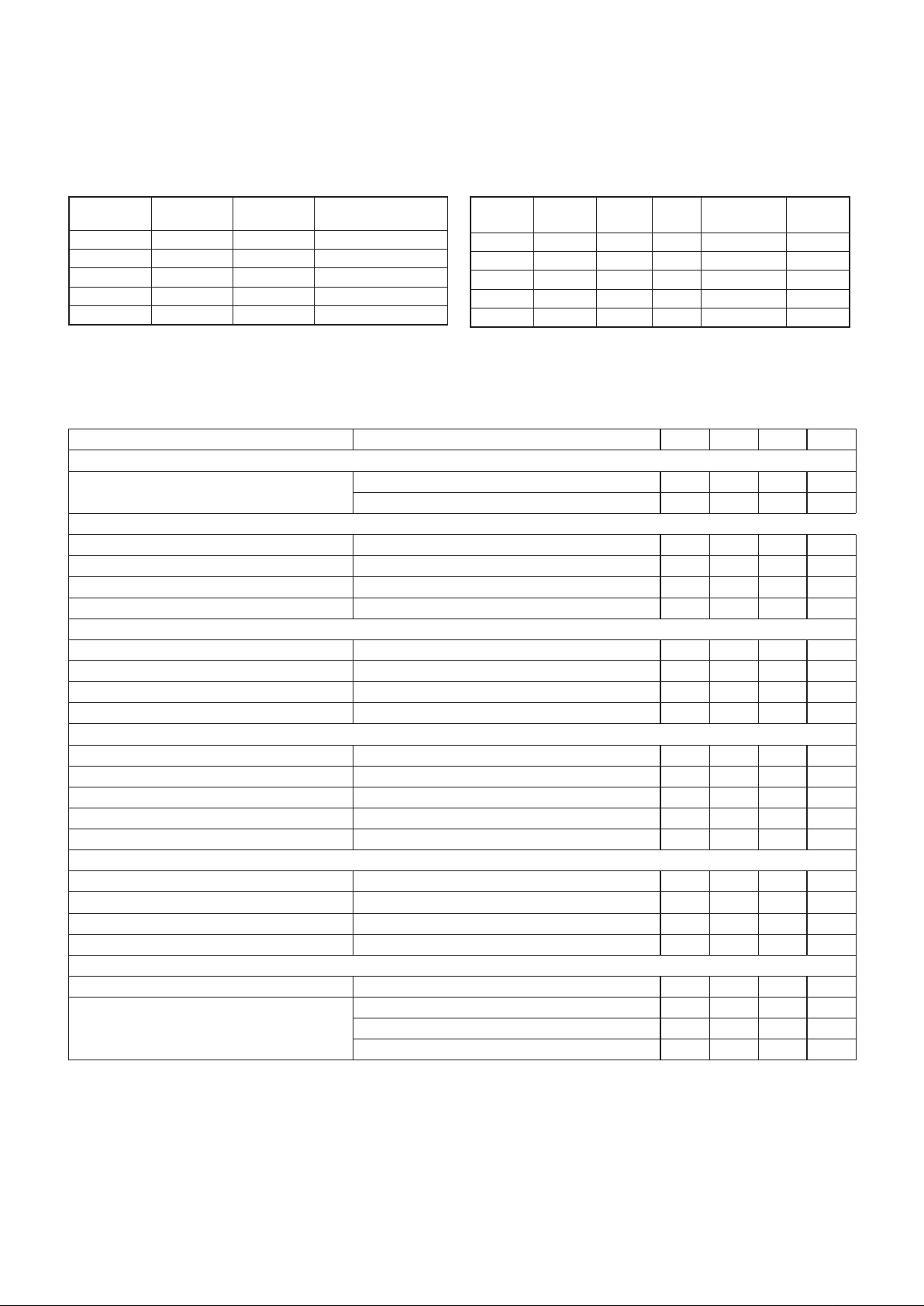
Table I. Frequency selectability decoding.
 Loading...