UCC3588
PRELIMINARY
DESCRIPTION
The UCC3588 synchronous step-down (Buck) regulator provides accurate
high efficiency power conversion. Using few external components, the
UCC1588 converts 5V to an adjustable output ranging from 3.5VDC to
2.1VDC in 100mV steps and 2.05VDC to 1.3VDC in 50mV steps with 1%
DC system accuracy. A high level of integration and novel design allow this
16-pin controller to provide a complete control solution for today’s
demanding microcontroller power requirements. Typical applications
include on board or VRM based power conversion for Intel Pentium II
microprocessors, as well as other processors from a variety of
manufacturers. High efficiency is obtained through the use of synchronous
rectification.
The softstart function provides a controlled ramp up of the system output
voltage. Overcurrent circuitry detects a hard (or soft) short on the system
output voltage and invokes a timed softstart/shutdown cycle to reduce the
PWM controller on time to 5%.
The oscillator frequency is externally programmed with RT and operates
over a range of 50kHz to 800kHz. The gate drivers are low impedance totem pole output stages capable of driving large external MOSFETs. Cross
conduction is eliminated by fixed delay times between turn off and turn on
of the external high side and synchronous MOSFETs. The chip includes
undervoltage lockout circuitry which assures the correct logic states at the
outputs during power up and power down.
(continued)
5-Bit Programmable Output BiCMOS Power Supply Controller
FEATURES
•
5-Bit Digital-to-Analog Converter
(DAC) supports Intel Pentium II
•
Microprocessor VID Codes
•
Compatible with 5V or 12V Systems
•
1% Output Voltage Accuracy
Guaranteed
•
Drives 2 N-Channel MOSFETs
•
Programmable Frequency to 800kHz
•
Power Good OV / UV / OVP Voltage
Monitor
•
Undervoltage Lockout and Softstart
Functions
• Short Circuit Protection
• Low Impedance MOSFET Drivers
• Chip Disable
SLUS311 - JULY 1999
4
11
15
5
6
7
8
3
16
12
9
10
1
2
14
13
UCC3588
VCC DRVHI
PWRGOOD
D0
D1
D2
D3
D4
SS/ENBL GND
COMP
VFB
VSENSE
ISNS
DRVLO
RT
R2
47k
C5
33nF
C16
10µF
R1
10K
C4C3C2C1
++++
RTN
D0
D1
D2
D3
D4
R3
200k
C6
220pF
C7 22pF
R7
15k
C13
1nF
R8
20k
R4
3Ω
R5
3Ω
R6
0.003Ω
C15
150µF
C12C11C10C8
+
+
RTN
VOUT
L1
1.6µH
Q2
IRL3103
Q1
IRL3103
D2D1
12V IN
5V IN
C8-C12 1500µF
+++
C1-C4
1500µF
+
C14
150µF
C9
+
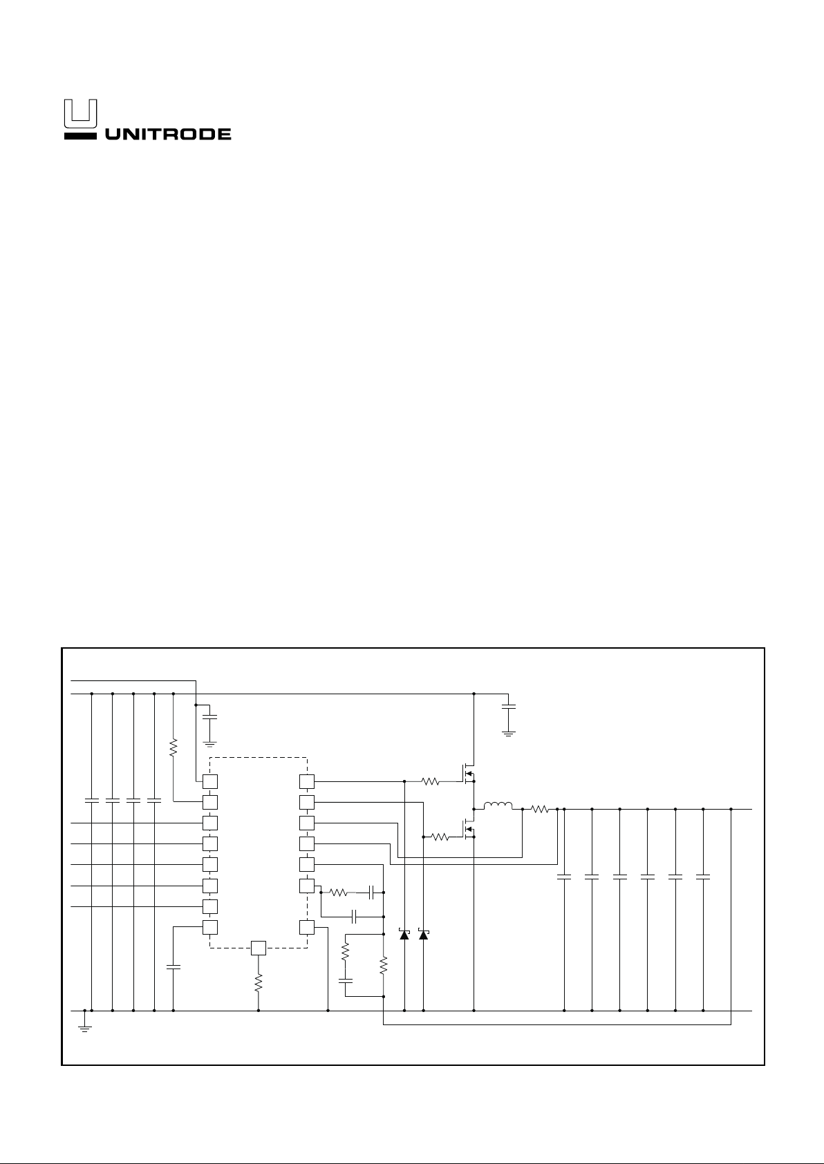
APPLICATION DIAGRAM
UDG-98158

2
UCC3588
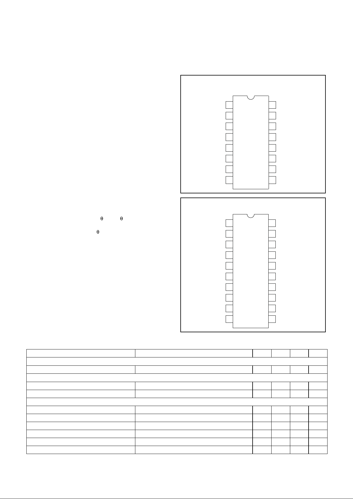
DIP-16, SOIC-16, TSSOP-16 (TOP VIEW)
N, J, D and PW Packages
ABSOLUTE MAXIMUM RATINGS
Supply Voltage VCC. . . . . . . . . . . . . . . . . . . . . . . . . . . . . . 15V
Gate Drive Current, 50% Duty Cycle. . . . . . . . . . . . . . . . . . 1A
Input Voltage, V
SENSE,VFB
, SS, COMMAND, COMP. . . . . 5V
Input Voltage, D0, D1, D2, D3, D4 . . . . . . . . . . . . . . . . . . . 6V
Input Current, RT, COMP . . . . . . . . . . . . . . . . . . . . . . . . . 5mA
Currents are positive into, negative out of the specified termi
-
nal. Consult Packaging Section of Databook for thermal limita
tions and considerations of packages. All voltages are
referenced to GND.
THERMAL DATA
Plastic DIP Package
Thermal Resistance Junction to Leads, θjc . . . . . . . . 45°C/W
Thermal Resistance Junction to Ambient, θja . . . . . . 90°C/W
Ceramic DIP Package
Thermal Resistance Junction to Leads, θjc . . . . . . . . 28°C/W
Thermal Resistance Junction to Ambient, θja . . . . . 120°C/W
Standard Surface Mount Package
Thermal Resistance Junction to Leads, θjc . . . . . . . . 35°C/W
Thermal Resistance Junction to Ambient, θja . . . . . 120°C/W
Note: The above numbers for ja and jc are maximums for
the limiting thermal resistance of the package in a standard
mounting configuration. The
ja numbers are meant to be
guidelines for the thermal performance of the device and
PC-board system. All of the above numbers assume no ambient airflow, see the packaging section of Unitrode Product Data
Handbook for more details.
RT16
15
14
13
12
11
10
9
1
2
3
4
5
6
7
8
VCC
DRVLO
DRVHI
GND
PWRGOOD
VFB
COMP
VSENSE
ISNS
SS/ENBL
D0
D1
D2
D3
D4
CONNECTION DIAGRAMS
ELECTRICAL CHARACTERISTICS:
Unless otherwise stated, these specifications hold for TA= 0°C to 70°C. TA=TJ.
V
CC
= 12V, RT = 49k.
PARAMETER TEST CONDITIONS MIN TYP MAX UNITS
Supply Current Section
Supply Current, On V
CC
= 12V, VRT= 2V 4.5 5.5 mA
UVLO Section
VCC UVLO Turn-On Threshold 10.05 10.50 10.85 V
UVLO Threshold Hysteresis 350 450 550 mV
Voltage Error Amplifier Section
Input Bias Current V
CM
= 2.0V –0.025 –0.050 µA
Open Loop Gain (Note 5) 77 dB
Output Voltage High I
COMP
= –500µA 3.5 3.6 V
Output Voltage Low I
COMP
= +500µA 0.2 0.5 V
Output Source Current V
VFB
= 2V, V
COMMAND=VCOMP
= 2.5V –400 –500 µA
Output Sink Current V
VFB
= 3V, V
COMMAND=VCOMP
= 2.5V 5 10 mA
This device is available in 16- pin surface mount, plastic
and ceramic DIP, TSSOP packages, and 20 pin surface
mount. The UCC3588 is specified for operation from 0°C
to +70°C.
DESCRIPTION (cont.)
PVCC
VCC
RT
DRVLO
DRVHI
GND
PGND
PWRGOOD
ISNS
VSENSE
N/C
D1
D2
SS/ENBL
N/C
D0
D4
D3 VFB
20
19
18
17
16
15
14
13
12
11
1
2
3
4
5
6
7
8
9
10 COMP
SOIC-20 (TOP VIEW)
DW Package

3
UCC3588
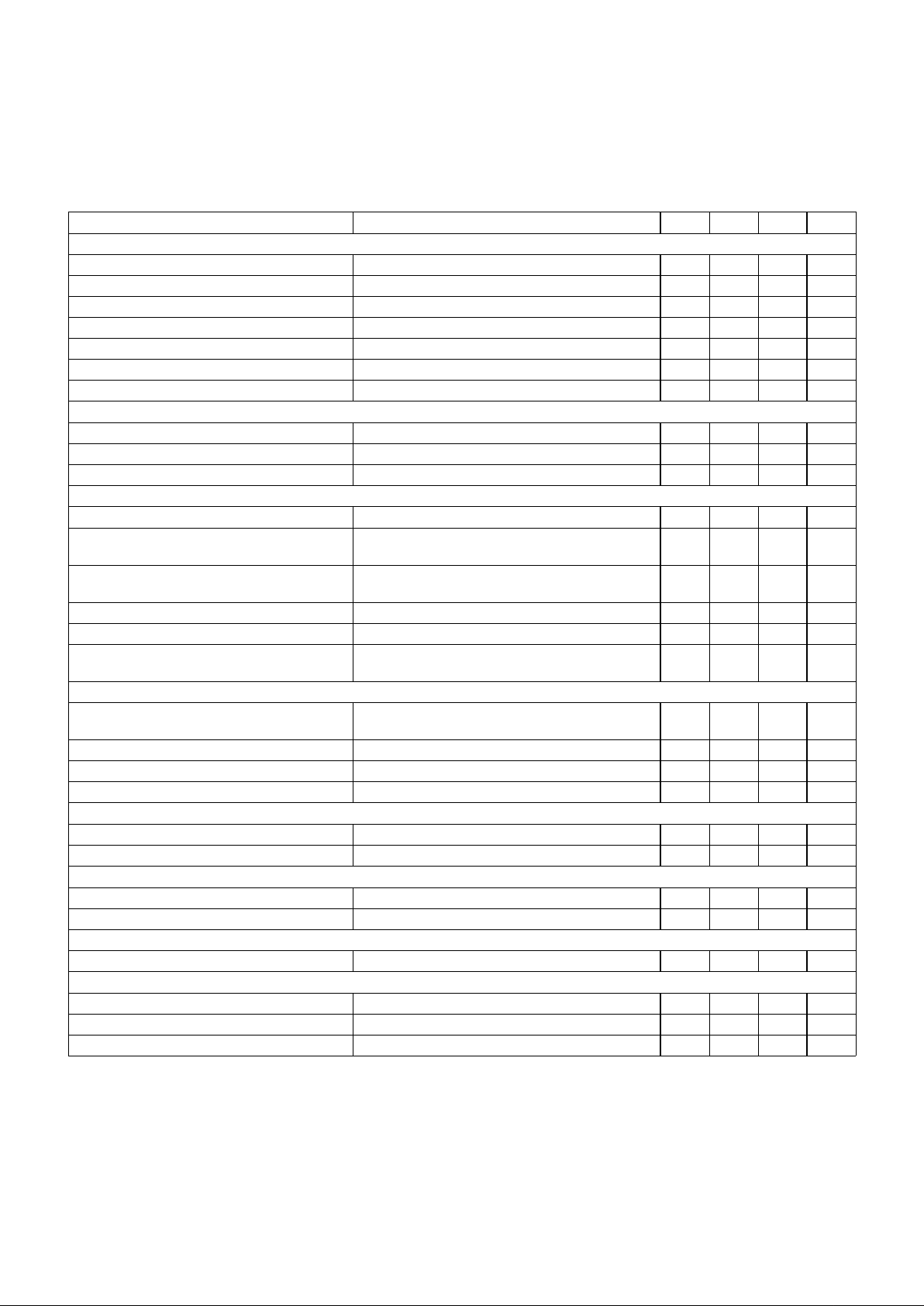
ELECTRICAL CHARACTERISTICS:
Unless otherwise stated, these specifications hold for TA= 0°C to 70°C. TA=TJ.
V
CC
= 12V, RT = 49k.
PARAMETER TEST CONDITIONS MIN TYP MAX UNITS
Oscillator/PWM Section
Initial Accuracy 0°C <T
A
< 70°C 250 270 290 kHz
Ramp Amplitude (p–p) 1.85 V
Ramp Valley Voltage 0.65 V
PWM Max Duty Cycle COMP = 3V (Note 5) 100 %
PWM Min Duty Cycle COMP = 0. 3V (Note 5) 0 %
PWM Delay to Outputs (High to Low) COMP = 1.5V (Note 5) 150 ns
PWM Delay to Outputs (Low to High) COMP = 1.5V (Note 5) 150 ns
Transient Window Comparator Section
Detection Range High (Duty Cycle = 0) % Over V
COMMAND
, (Note 1) 3 %
Detection Range Low (Duty Cycle = 1) % Under V
COMMAND
, (Note 1) –3 %
Propagation Delay (V
SENSE
to Outputs) 150 200 nS
Soft Start/ Shutdown Section
SS Charge Current (Normal Start Up) Measured on SS –6 –12 µA
SS Charge Current (Short Circuit Fault
Condition)
Measured on SS –60 –100 –120 µA
SS Discharge Current (During Timeout
Sequence)
Measured on SS 1 2.5 5 µA
Shutdown Threshold Measured on SS 4.1 4.2 4.3 V
Restart Threshold Measured on SS 0.4 0.5 0.6 V
Soft Start Complete Threshold (Normal
Start-Up)
Measured on SS 3.5 3.7 3.9 V
DAC / Reference Section
COMMAND Voltage Accuracy 10.8V <V
CC
< 13.2V, measured on COMP,
0°C < T
A
< +70°C, (Note 2)
–1.0 1.0 %
D0–D4 Voltage High 5.5 6 6.5 V
D0–D4 Voltage Threshold 2.5 3.0 3.5 V
D0–D4 Voltage Input Bias Current V(D4,...,D0) < 0.5V –80 –100 µA
Overvoltage Comparator Section
Trip Point % Over V
COMMAND
, (Note 1) 8 12 %
Hysteresis 10 20 35 mV
Undervoltage Comparator Section
Trip Point % Under V
COMMAND
, (Note 1) –8.0 –12.0 %
Hysteresis 10 20 35 mV
PWRGOOD Signal Section
Output Impedance V
CC
= 12V, I
PWRGOOD
= 1mA 470 Ω
Overvoltage Protection Section
Trip Point % Over V
COMMAND
, (Note 1) 15 17.5 20 %
Hysteresis 20 35 mV
VSENSE Input Bias Current OV, OVP, UV Combined –8 –12 –16 µA

4
UCC3588
ELECTRICAL CHARACTERISTICS:
Unless otherwise stated, these specifications hold for TA= 0°C to 70°C. TA=TJ.
V
CC
= 12V, RT = 49k.
PARAMETER TEST CONDITIONS MIN TYP MAX UNITS
Gate Drivers (DRVHI, DRVLO) Section
Output High Voltage I
GATE
= 100mA, VCC= 12V 10.8 11.5 V
Output Low Voltage I
GATE
=– 100mA, VCC= 12V 0.5 0.8 V
Driver Non-overlap Time
(DRVHI– to DRVLO+)
(Note 3) 90 120 150 ns
Driver Non-overlap Time
(DRVLO– to DRVHI+)
(Note 3) 50 80 120 ns
Driver Rise Time 3nF Capacitive Load 80 100 ns
Driver Fall Time 3nF Capacitive Load 80 100 ns
Current Limit Section
Start of Quick Charge to Shutdown
Threshold
V
ISNS=VSENSE
+ 75mV, CSS= 10nF, (Note 4)
(Note 5)
50 µs
Current Limit Threshold Voltage V
THRESHOLD=VISNS–VVSENSE
40 54 70 mV
ISNS Input Bias Current –8 –12 –16 µA
Note 1: This percentage is measured with respect to the ideal command voltage programmed by the VID(D0,....,D4) pins and ap
-
plies to all DAC codes from 1.3 to 3.5V.
Note 2: Reference and error amplifier offset trimmed while the voltage amp is set in unity gain mode.
Note 3: Deadtime delay is measured from the 50% point of DRVHI falling to the 50% point of DRVLO rising, and vice-verse.
Note 4: This time is dependent on the value of C
SS
.
Note 5: Guaranteed by design.Not 100% tested in production.
10
8
7
6
5
4
3
DAC
OVP
OV/UV
+
–
9
1
SOFTSTART
CURRENT
LIMIT
BLOCK
OVER-
CURRENT
2 11
OSC
16
R
S
Q
VREF
15
12
TURN
ON
DELAY
TURN
ON
DELAY
ANTI CROSS-
CONDUCTION
13
14
V
CC
UVLO
10.5V
VBIAS
VOLTAGE
AMPLIFIER
COMP
VFB
D4
D3
D2
D1
D0
SS/ENBL
ISNS VSENSE PWRGOOD RT
GND
VCC
DRVHI
DRVLO
COMMAND
–3%
COMMAND
+3%
VSENSE
DUTY=1
DUTY=0
SHUTDOWN
PWM
COMP.
COMMAND
SHUTDOWN
TO
VREF
SHUTDOWN
+
+
–+
–
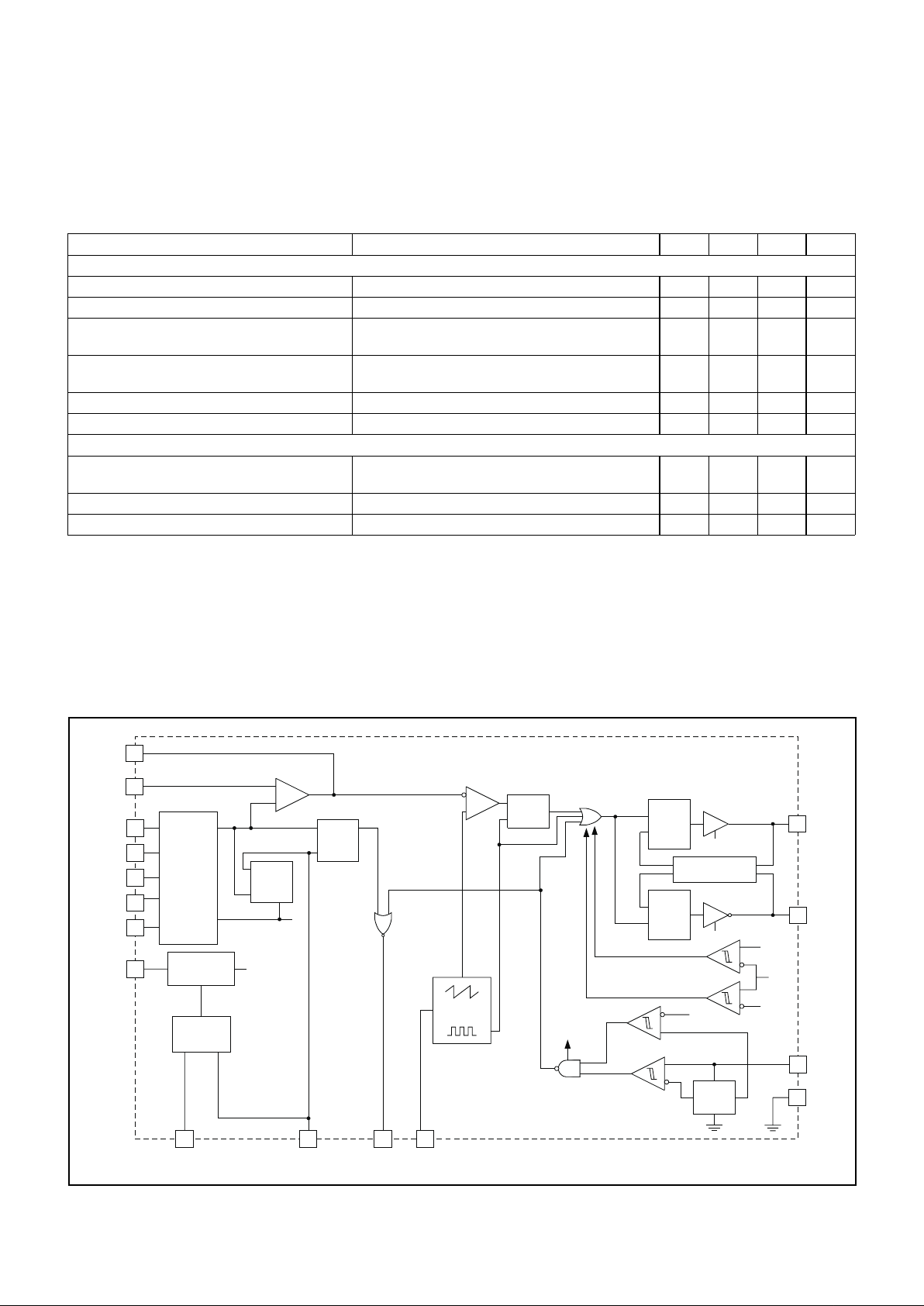
BLOCK DIAGRAM
UDG-98152
 Loading...