Texas Instruments UCC35701QTR, UCC35701Q, UCC35701PWTR, UCC35701PW, UCC35701N Datasheet
...
UCC15701/2
UCC25701/2
UCC35701/2
Advanced Voltage Mode Pulse Width Modulator
DESCRIPTION
The UCC35701/UCC35702 family of pulse width modulators is intended for
isolated switching power supplies using primary side control. They can be
used for both off-line applications and DC/DC converter designs such as in
a distributed power system architecture or as a telecom power source.
The devices feature low startup current, allowing for efficient off-line start
ing, yet have sufficient output drive to switch power MOSFETs in excess of
500kHz.
Voltage feed forward compensation is operational over a 5:1 input range
and provides fast and accurate response to input voltage changes over a
4:1 range. An accurate volt-second clamp and maximum duty cycle limit
are also featured.
Fault protection is provided by pulse by pulse current limiting as well as the
ability to latch off after a programmable number of repetitive faults has oc
curred.
Two UVLO options are offered. UCC35701 family has turn-on and turn-off
thresholds of 13V/9V and UCC35702 family has thresholds of 9.6V/8.8V.
The UCC35701/2 and the UCC25701/2 are offered in the 14 pin SOIC (D),
14 pin PDIP (N) or in 14 pin TSSOP (PW) packages. The UCC15701/2 is
offered in the 14 pin CDIP (J) package.
3VDD
12 VREF
8FB
4OUT
2ILIM
5PGND
C3
1 COUNT
CF
14 SS
CS
11 SYNC
9 VSCLAMP
VREF
10 CT
CT
7RT
6
VFF
13GND
VINSUPPLY
V
IN
RETURN
RGND
R10
RCS
R8
R7
R6
C2
R8
R
F
R5
R4
R3
R2
R1
V
OUT
UCC35701
C1
C4
C6
R12
C6
C5
R11
R13
C7
R14
V
OUT
R15
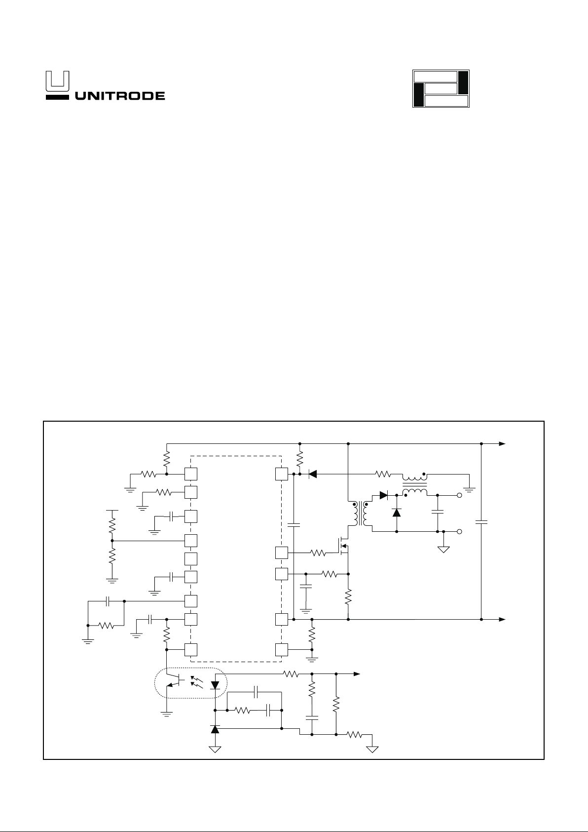
TYPICAL APPLICATION DIAGRAM
SLUS293A - JANUARY 2000
FEATURES
•
700kHz Operation
•
Integrated Oscillator/ Voltage Feed
Forward Compensation
•
Accurate Duty Cycle Limit
•
Accurate Volt-second Clamp
•
Optocoupler Interface
•
Fault Counting Shutdown
•
Fault Latch off or Automatic Shutdown
•
Soft Stop Optimized for Synchronous
Rectification
•
1A Peak Gate Drive Output
• 130µA Start-up Current
• 750µA Operating Current
UDG-98005-1
application
INFO
available

2
UCC15701/2
UCC25701/2
UCC35701/2
ABSOLUTE MAXIMUM RATINGS
Supply voltage (Supply current limited to 20mA) . . . . . . . . 15V
Supply Current. . . . . . . . . . . . . . . . . . . . . . . . . . . . . . . . . 20mA
Input pins ( ILIM,VFF,RT,CT,VSCLAMP,SYNC,SS) . . . . . . 6V
Output Current (OUT) DC. . . . . . . . . . . . . . . . . . . . . +/–180mA
Output Current (OUT) Pulse (0.5ms) . . . . . . . . . . . . . . +/–1.2A
Storage Temperature. . . . . . . . . . . . . . . . . . . –65°C to +150°C
Junction Temperature. . . . . . . . . . . . . . . . . . . –55°C to +150°C
Lead Temperature (Soldering, 10 sec.) . . . . . . . . . . . . +300°C
Note: All voltages are with respect to GND. Currents are posi
tive into the specified terminal. Consult Packaging Section of
the Databook for thermal limitations and considerations of
packages.
VREF
GND
SS
SYNC
CT
FB
VSCLAMP
1
2
3
4
5
6
7
14
13
12
11
10
9
8
ILIM
COUNT
VFF
RT
VDD
OUT
PGND
CONNECTION DIAGRAMS
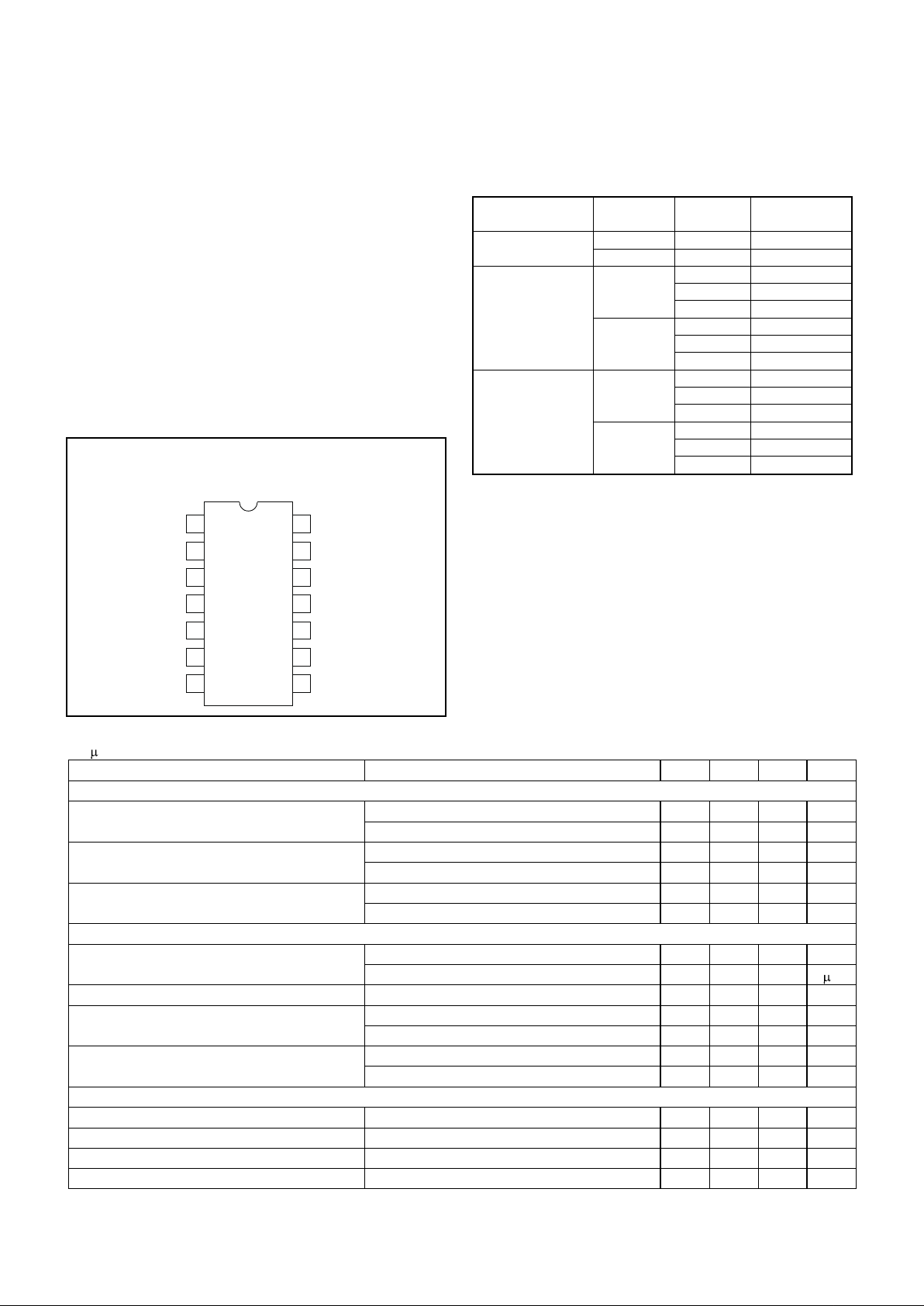
DIL-14, SOIC-14,TSSOP-14 (TOP VIEW)
N or J, D, PW PACKAGE
ELECTRICAL CHARACTERISTICS: Unless otherwise specified, V
DD
= 11V, RT = 60.4k, CT= 330pF, C
REF=CVDD
=
0.1 F, VFF= 2.0V, and no load on the outputs.
PARAMETER TEST CONDITIONS MIN TYP MAX UNITS
UVLO Section
Start Threshold (UCCX5701) 12 13 14 V
(UCCX5702) 8.8 9.6 10.4 V
Stop Threshold (UCCX5701) 8 9 10 V
(UCCX5702) 8.0 8.8 9.6 V
Hysteresis (UCCX5701) 3 4 V
(UCCX5702) 0.3 0.8 V
Supply Current
Start-up Current (UCCX5701) V
DD
= 11V, VDDComparator Off 130 200 µA
(UCCX5702) V
DD
= 8V, VDDComparator Off 120 190 A
I
DD
Active VDDComparator On 0.75 1.5 mA
V
DD
Clamp Voltage (UCCX5701) IDD= 10mA 13.5 14.3 15 V
(UCCX5702) I
DD
= 10mA 13 13.8 15 V
V
DD
Clamp – Start Threshold (UCCX5701) 1.3 V
(UCCX5702) 4.2 V
Voltage Reference
V
REF
VDD= 10V to 13V, I
VREF
= 0mA to 2mA 4.9 5 5.1 V
Line Regulation V
DD
= 10V to 13V 20 mV
Load Regulation I
VREF
= 0mA to 2mA 2 mV
Short Circuit Current V
REF
= 0V, TJ = 25°C 20 50 mA
TA=T
J
UVLO
Option
Package Part Number
–55°C to +125°C
13V / 9V CDIP-14 UCC15701J
9.6V / 8.8V CDIP-14 UCC15702J
–40°C to +85°C
13V / 9V
SOIC-14 UCC25701D
PDIP-14 UCC25701N
TSSOP-14 UCC25701PW
9.6V / 8.8V
SOIC-14 UCC25702D
PDIP-14 UCC25702N
TSSOP-14 UCC25702PW
0°C to +70°C
13V / 9V
SOIC-14 UCC35701D
PDIP-14 UCC35701N
TSSOP-14 UCC35701PW
9.6V / 8.8V
SOIC-14 UCC35702D
PDIP-14 UCC35702N
TSSOP-14 UCC35702PW
The D and PW packages are available taped and reeled. Add
TR suffix to the device type (e.g., UCC35701DTR).
ORDERING INFORMATION

3
UCC15701/2
UCC25701/2
UCC35701/2
ELECTRICAL CHARACTERISTICS:
Unless otherwise specified, VDD= 11V, RT = 60.4k, CT= 330pF, C
REF=CVDD
=
0.1 F, VFF= 2.0V, and no load on the outputs.
PARAMETER TEST CONDITIONS MIN TYP MAX UNITS
Line Sense
Vth High Line Comparator 3.9 4 4.1 V
Vth Low Line Comparator 0.5 0.6 0.7 V
Input Bias Current –100 100 nA
Oscillator Section
Frequency V
FF
= 0.8V to 3.2V 90 100 110 kHz
Frequency V
FF
= 0.6V to 3.4V (Note 1) 90 100 110 kHz
SYNC VIH 2V
SYNC VIL 0.8 V
SYNC Input Current VSYNC = 2.0V 3 10 µA
RT Voltage VFF = 0.4V 0.5 0.6 0.7 V
VFF = 0.8V 0.75 0.8 0.85 V
VFF = 2.0V 1.95 2.0 2.05 V
VFF = 3.2V 3.15 3.2 3.25 V
VFF = 3.6V 3.3 3.4 3.5 V
C
T
Peak Voltage VFF = 0.8V (Note 1) 0.8 V
VFF = 3.2V (Note 1) 3.2 V
C
T
Valley Voltage (Note 1) 0 V
Soft Start/Shutdown/Duty Cycle Control Section
I
SS
Charging Current 10 18 30 A
I
SS
Discharging Current 300 500 750 µA
Saturation V
DD
= 11V, IC Off 25 100 mV
Fault Counter Section
Threshold Voltage VFF = 0.8V to 3.2V 3.8 4 4.2 V
Saturation Voltage VFF = 0.8V to 3.2V 100 mV
Count Charging Current 10 18 30 µA
Current Limit Section
Input Bias Current –100 0 100 nA
Current Limit Threshold 180 200 220 mV
Shutdown Threshold 500 600 700 mV
Pulse Width Modulator Section
FB Pin Input Impedance VFB = 3V 30 50 100 k
Minimum Duty Cycle VFB <= 1V 0 %
Maximum Duty Cycle VFB >= 4.5V, VSCLAMP >= 2.0V 95 99 100 %
PWM Gain VFF = 0.8V 35 50 70 %/V
Volt Second Clamp Section
Maximum Duty Cycle VFF = 0.8V, VSCLAMP = 0.6V 69 74 79 %
Minimum Duty Cycle VFF = 3.2V, VSCLAMP = 0.6V 17 19 21 %
Output Section
VOH I
OUT
= –100mA, (VDD–V
OUT
) 0.4 1 V
VOL I
OUT
= 100mA 0.4 1 V
Rise Time C
LOAD
= 1000pF 20 100 ns
Fall Time C
LOAD
= 1000pF 20 100 ns
Note 1: Guaranteed by design. Not 100% tested in production.
 Loading...