

UCC1580-1,-2,-3,-4
UCC2580-1,-2,-3,-4
UCC3580-1,-2,-3,-4
SLUS292 - FEBRUARY 1999
FEATURES
• Provides Auxiliary Switch Activation
Complementary to Main Power
Switch Drive
• Programmable deadtime (Turn-on
Delay) Between Activation of Each
Switch
• Voltage Mode Control with
Feedforward Operation
• Programmable Limits for Both
Transformer Volt- Second Product
and PWM Duty Cycle
• High Current Gate Driver for Both
Main and Auxiliary Outputs
• Multiple Protection Features with
Latched Shutdown and Soft Restart
• Low Supply Current (100µA Startup,
1.5mA Operation)
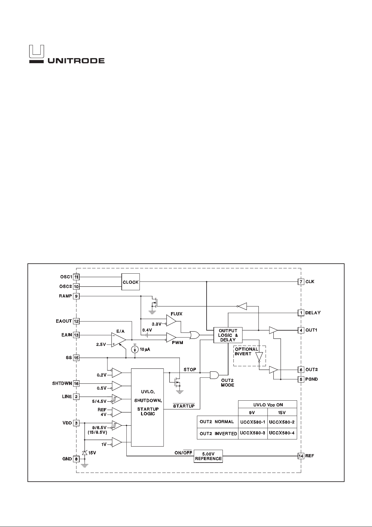
BLOCK DIAGRAM
DESCRIPTION
The UCC3580 family of PWM controllers is designed to implement a variety
of active clamp/reset and synchronous rectifier switching converter topologies. While containing all the necessary functions for fixed frequency, high
performance pulse width modulation, the additional feature of this design is
the inclusion of an auxiliary switch driver which complements the main
power switch, and with a programmable deadtime or delay between each
transition. The active clamp/reset technique allows operation of single
ended converters beyond 50% duty cycle while reducing voltage stresses
on the switches, and allows a greater flux swing for the power transformer.
This approach also allows a reduction in switching losses by recovering energy stored in parasitic elements such as leakage inductance and switch
capacitance.
The oscillator is programmed with two resistors and a capacitor to set
switching frequency and maximum duty cycle. A separate synchronized
ramp provides a voltage feedforward pulse width modulation and a programmed maximum volt-second limit. The generated clock from the oscillator contains both frequency and maximum duty cycle information.
(continued)
Single Ended Active Clamp/Reset PWM
UDG-95069-2
Pin Numbers refer to DIL-16 and SOIC-16 packages
2
UCC1580-1,-2,-3,-4
UCC2580-1,-2,-3,-4
UCC3580-1,-2,-3,-4
VDD. . . . . . . . . . . . . . . . . . . . . . . . . . . . . . . . . . . . . . . . . . . 16V
I
VDD
. . . . . . . . . . . . . . . . . . . . . . . . . . . . . . . . . . . . . . . . . . 25mA
LINE, RAMP . . . . . . . . . . . . . . . . . . . . . . . . −0.3V to VDD + 1V
I
LINE
, I
RAMP
. . . . . . . . . . . . . . . . . . . . . . . . . . . . . . . . . . . . . 5mA
DELAY . . . . . . . . . . . . . . . . . . . . . . . . . . . . . . . . . . . . . . . . 5.3V
I
DELAY
. . . . . . . . . . . . . . . . . . . . . . . . . . . . . . . . . . . . . . . . −5mA
I
OUT1
(tpw < 1µs and Duty Cycle < 10%). . . . . . . −0.6A to 1.2A
I
OUT2
(tpw < 1µs and Duty Cycle < 10%). . . . . . . −0.4A to 0.4A
I
CLK
. . . . . . . . . . . . . . . . . . . . . . . . . . . . . . . . −100mA to 100mA
OSC1, OSC2, SS, SHTDWN, EAIN . . . . . −0.3V to REF + 0.3V
I
EAOUT
. . . . . . . . . . . . . . . . . . . . . . . . . . . . . . . . . . −5mA to 5mA
I
REF
. . . . . . . . . . . . . . . . . . . . . . . . . . . . . . . . . . . . . . . . . −30mA
PGND. . . . . . . . . . . . . . . . . . . . . . . . . . . . . . . . . . −0.2V to 0.2V
Storage Temperature . . . . . . . . . . . . . . . . . . . −65°C to +150°C
Junction Temperature. . . . . . . . . . . . . . . . . . . −55°C to +150°C
Lead Temperature (Soldering, 10 sec.). . . . . . . . . . . . . +300°C
All voltages are with respect to ground unless otherwise stated.
Currents are positive into, negative out of the specified terminal. Consult Packaging Section of Databook for thermal limitations and considerations of packages.
ABSOLUTE MAXIMUM RATINGS
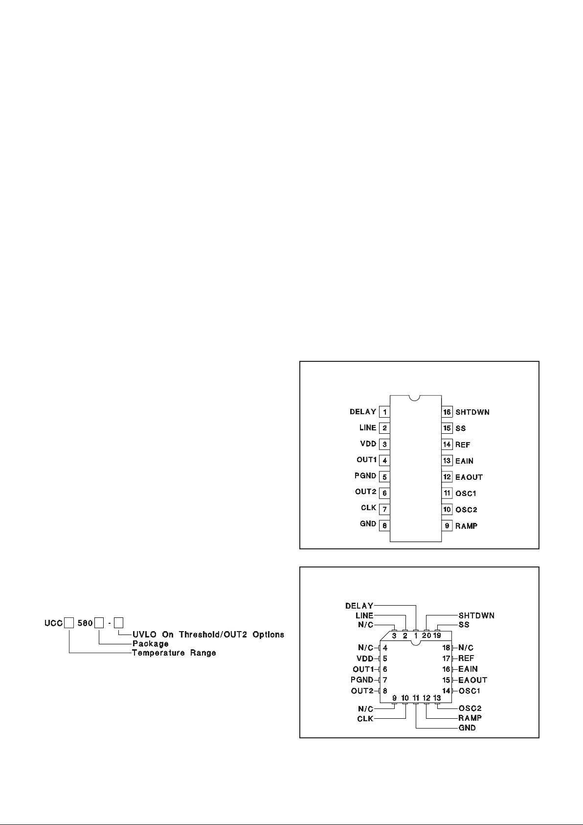
PLCC-20 (Top View)
Q Packages
CONNECTION DIAGRAMS
DIL-16, SOIC-16 (Top View)
J, N, or D Packages
ORDER INFORMATION
The main gate drive output (OUT1) is controlled by the
pulse width modulator. The second output (OUT2) is intended to activate an auxiliary switch during the off time
of the main switch, except that between each transition
there is deadtime where both switches are off, programmed by a single external resistor. This design offers
two options for OUT2, normal and inverted. In the -1 and
-2 versions, OUT2 is normal and can be used to drive
PMOS FETs. In the -3 and -4 versions, OUT2 is inverted
and can be used to drive NMOS FETs. In all versions,
both the main and auxiliary switches are held off prior to
startup and when the PWM command goes to zero duty
cycle. During fault conditions, OUT1 is held off while
OUT2 operates at maximum duty cycle with a guaranteed off time equal to the sum of the two deadtimes.
Undervoltage lockout monitors supply voltage (VDD), the
precision reference (REF), input line voltage (LINE), and
the shutdown comparator (SHTDWN). If after any of
these four have sensed a fault condition, recovery to full
operation is initiated with a soft start. VDD thresholds, on
and off, are 15V and 8.5V for the -2 and -4 versions, 9V
and 8.5V for the -1 and -3 versions.
The UCC1580-x is specified for operation over the military temperature range of −55°C to 125°C. The
UCC2580-x is specified from −40°C to 85°C. The
UCC3580-x is specified from 0°C to 70°C. Package options include 16-pin surface mount or dual in-line, and
20-pin plastic leadless chip carrier.
DESCRIPTION (cont.)

3
UCC1580-1,-2,-3,-4
UCC2580-1,-2,-3,-4
UCC3580-1,-2,-3,-4
ELECTRICAL CHARACTERISTICS
Unless otherwise stated, all specifications are over the full temperature range, VDD
= 12V, R1 = 18.2k, R2 = 4.41k, CT= 100pF, R3 = 100k, C
OUT1
= 0, C
OUT2
= 0. TA= 0°C to 70°C for the UCC3580, −40°C to 85°C
for the UCC2580, −55°C to 125°C for the UCC1580, TA= TJ.
PARAMETER TEST CONDITIONS MIN TYP MAX UNITS
Oscillator Section
Frequency 370 400 430 kHz
CLK Pulse Width 650 750 850 ns
CLK V
OH
I
CLK
= −3mA 4.3 4.7 V
CLK V
OL
I
CLK
= 3mA 0.3 0.5 V
Ramp Generator Section
Ramp V
OL
I
RAMP
= 100µA 50 100 mV
Flux Comparator Vth 3.16 3.33 3.50 V
Pulse Width Modulator Section
Minimum Duty Cycle OUT1, EAOUT = VOL 0 %
Maximum Duty Cycle OUT1, EAIN = 2.6V 63 66 69 %
PWM Comparator Offset 0.1 0.4 0.9 V
Error Amplifier Section
EAIN EAOUT = EAIN 2.44 2.5 2.56 V
I
EAIN
EAOUT = EAIN 150 400 nA
EAOUT, VOL EAIN = 2.6V, I
EAOUT
= 100µA 0.3 0.5 V
EAOUT, VOH EAIN = 2.4V, I
EAOUT
= −100µA 4 5 5.5 V
AVOL 70 80 dB
Gain Bandwidth Product f = 100kHz (Note 1) 2 6 MHz
Softstart/Shutdown Section
Start Duty Cycle EAIN = 2.4V 0 %
SS V
OL I
SS
= 100µA 100 350 mV
SS Restart Threshold 400 550 mV
I
SS
–20 –35 µA
SHTDWN V
TH
0.4 0.5 0.6 V
I
SHTDWN
50 150 nA
Undervoltage Lockout Section
VDD On UCC3580-2,-4 14 15 16 V
UCC3580-1,-3 8 9 10 V
VDD Off 7.5 8.5 9.5 V
LINE On 4.7 5 5.3 V
LINE Off 4.2 4.5 4.8 V
I
LINE
LINE = 6V 50 150 nA
Supply Section
VDD Clamp I
VDD
= 10mA 14 15 16 V
I
VDD
Start VDD < VDD On 160 250 µA
I
VDD
Operating No Load 2.5 3.5 mA
Output Drivers Section
OUT1 V
SAT
High I
OUT1
= −50mA 0.4 1.0 V
OUT1 V
SAT
Low I
OUT1
=100mA 0.4 1.0 V
OUT2 V
SAT
High I
OUT2
= −30mA 0.4 1.0 V
OUT2 V
SAT
Low I
OUT2
= 30mA 0.4 1.0 V
OUT1 Fall Time C
OUT1
= 1nF, RS = 3Ω 20 50 ns
OUT1 Rise Time C
OUT1
= 1nF, RS = 3Ω 40 80 ns
OUT2 Fall Time C
OUT2
= 300pF, RS = 10Ω 20 50 ns
4
UCC1580-1,-2,-3,-4
UCC2580-1,-2,-3,-4
UCC3580-1,-2,-3,-4
ELECTRICAL CHARACTERISTICS
Unless otherwise stated, all specifications are over the full temperature range, VDD
= 12V, R1 = 18.2k, R2 = 4.41k, CT= 100pF, R3 = 100k, C
OUT1
= 0, C
OUT2
= 0. TA= 0°C to 70°C for the UCC3580, −40°C to 85°C
for the UCC2580, −55°C to 125°C for the UCC1580, TA= TJ.
PARAMETER TEST CONDITIONS MIN TYP MAX UNITS
Output Drivers Section (cont.)
OUT2 Rise Time C
OUT2
= 300pF, RS= 10Ω 20 40 ns
Delay 1 OUT2 to OUT1 R3 = 100k, C
OUT1
= C
OUT2
= 15pF 90 120 160 ns
T
A
= TJ= 25°C 100 120 140 ns
Delay 2 OUT1 to OUT2 R3 = 100k, C
OUT1
= C
OUT2
= 15pF 110 170 250 ns
T
A
= TJ= 25°C 140 170 200 ns
Reference Section
REF I
REF
= 0 4.875 5 5.125 V
Load Regulation I
REF
= 0mA to 1mA 1 20 mV
Line Regulation VDD = 10V to 14V 1 20 mV
CLK: Oscillator clock output pin from a low impedance
CMOS driver. CLK is high during guaranteed off time.
CLK can be used to synchronized up to five other
UCC3580 PWMs.
DELAY: A resistor from DELAY to GND programs the
nonoverlap delay between OUT1 and OUT2. The delay
times, Delay1 and Delay2, are shown in Figure 1 and are
as follows:
Delay pF R
111 3=•.
Delay2 is designed to be larger than Delay1 by a ratio
shown in Figure 2.
EAIN: Inverting input to the error amplifier. The
noninverting input of the error amplifier is internally set to
2.5V. EAIN is used for feedback and loop compensation.
EAOUT: Output of the error amplifier and input to the
PWM comparator. Loop compensation components
connect from EAOUT to EAIN.
GND: Signal Ground.
LINE: Hysteretic comparator input. Thresholds are 5.0V
and 4.5V. Used to sense input line voltage and turn off
OUT1 when the line is low.
OSC1 & OSC2: Oscillator programming pins. A resistor
connects each pin to a timing capacitor. The resistor
connected to OSC1 sets maximum on time. The resistor
connected to OSC2 controls guaranteed off time. The
combined total sets frequency with the timing capacitor.
Frequency and maximum duty cycle are approximately
given by:
()
Frequency
1
R1 1.25 R2 CT
=
+••
Maximum Duty Cycle
R1
R1 1.25 R2
=
+•
Maximum Duty Cycle for OUT1 will be slightly less due to
Delay1 which is programmed by R3.
OUT1: Gate drive output for the main switch capable of
sourcing up to 0.5A and sinking 1A.
OUT2: Gate drive output for the auxiliary switch with
± 0.3A drive current capability.
PGND: Ground connection for the gate drivers. Connect
PGND to GND at a single point so that no high frequency
components of the output switching currents are in the
ground plane on the circuit board.
RAMP: A resistor (R4) from RAMP to the input voltage
and a capacitor (CR) from RAMP to GND programs the
feedforward ramp signal. RAMP is discharged to GND
when CLK is high and allowed to charge when CLK is
low. RAMP is the line feedforward sawtooth signal for the
PWM comparator. Assuming the input voltage is much
greater than 3.3V, the ramp is very linear. A flux
comparator compares the ramp signal to 3.3V to limit the
maximum allowable volt-second product:
Volt-Second Product Clamp = 3.3 • R4 • CR.
REF: Precision 5.0V reference pin. REF can supply up to
5mA to external circuits. REF is off until VDD exceeds 9V
(–1 and –3 versions) or activates the 15V clamp (–2 and
–4 versions) and turns off again when VDD droops below
8.5V. Bypass REF to GND with a 1µF capacitor.
SHTDWN: Comparator input to stop the chip. The
threshold is 0.5V. When the chip is stopped, OUT1 is low
and OUT2 continues to oscillate with guaranteed off time
equal to two non-overlap delay times.
PIN DESCRIPTIONS

5
UCC1580-1,-2,-3,-4
UCC2580-1,-2,-3,-4
UCC3580-1,-2,-3,-4
UVLO and Startup
For self biased off-line applications, -2 and -4 versions
(UVLO on and off thresholds of 15V and 8.5V typical)
are recommended. For all other applications, -1 and -3
versions provide the lower on threshold of 9V. The IC requires a low startup current of only 160µA when VDD is
under the UVLO threshold, enabling use of a large trickle
charge resistor (with corresponding low power dissipation) from the input voltage. VDD has an internal clamp
at 15V which can sink up to 10mA. Measures should be
taken not to exceed this current. For -2 and -4 versions,
this clamp must be activated as an indication of reaching
the UVLO on threshold. The internal reference (REF) is
brought up when the UVLO on threshold is crossed. The
startup logic ensures that LINE and REF are above and
SHTDWN is below their respective thresholds before
outputs are asserted. LINE input is useful for monitoring
actual input voltage and shutting off the IC if it falls below a programmed value. A resistive divider should be
used to connect the input voltage to the LINE input. This
feature can protect the power supply from excessive
currents at low line voltages.
Figure 1. Output time relationships.
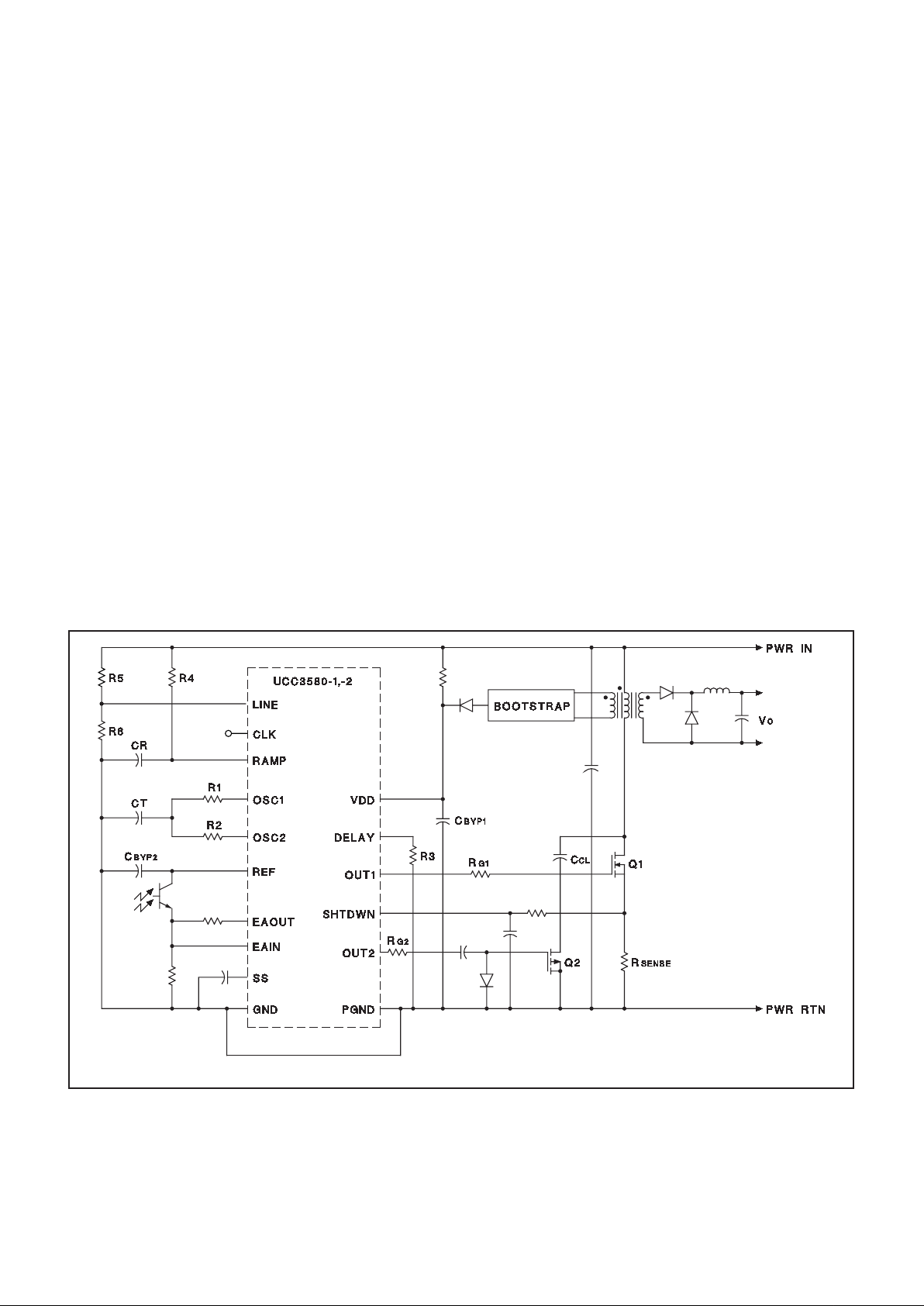
APPLICATION INFORMATION
UDG-95070-2
Note: Waveforms are not to scale.
SS: A capacitor from SS to ground programs the soft
start time. During soft start, EAOUT follows the amplitude
of SS’s slowly increasing waveform until regulation is
achieved.
VDD: Chip power supply pin. VDD should be bypassed
to PGND. The –1 and –3 versions require VDD to ex-
ceed 9V to start and remain above 8.5V to continue running. A shunt clamp from VDD to GND limits the supply
voltage to 15V. The –2 and –4 versions do not start until
the shunt clamp threshold is reached and operation continues as long as VDD is greater than 8.5V.
PIN DESCRIPTIONS (cont.)

6
UCC1580-1,-2,-3,-4
UCC2580-1,-2,-3,-4
UCC3580-1,-2,-3,-4
The soft start pin provides an effective means to start
the IC in a controlled manner. An internal current of
20µA begins charging a capacitor connected to SS once
the startup conditions listed above have been met. The
voltage on SS effectively controls maximum duty cycle
on OUT1 during the charging period. OUT2 is also controlled during this period (see Figure 1). Negation of any
of the startup conditions causes SS to be immediately
discharged. Internal circuitry ensures full discharge of
SS (to 0.3V) before allowing charging to begin again,
provided all the startup conditions are again met.
Oscillator
Simplified oscillator block diagram and waveforms are
shown in Figure 3. OSC1 and OSC2 pins are used to
program the frequency and maximum duty cycle. Capacitor CT is alternately charged through R1 and discharged through R2 between levels of 1V and 3.5V. The
charging and discharging equations for CT are given by
VC(charge)= REF – 4.0 •e
-
t
1
τ
VC(discharge)= 3.5 • e
-
t
2
τ
where τ1=R1•CT andτ2= R2 • CT. The charge time
and discharge time are given by
t
CH = R1 • CT and tDIS = 1.25 • R2 • CT
The CLK output is high during the discharge period. It
blanks the output to limit the maximum duty cycle of
OUT1. The frequency and maximum duty cycle are
given by
Frequency =
1
(R1+1.25 •R2) •CT
MaximumDutyCycle =
R1
R1+1.25 •R2
Maximum Duty Cycle for OUT1 will be slightly less due
to Delay1 which is programmed by R3.
Voltage Feedforward and Volt-Second Clamp
UCC3580 has a provision for input voltage feedforward.
As shown in Figure 3, the ramp slope is made proportional to input line voltage by converting it into a charging current for CR. This provides a first order
cancellation of the effects of line voltage changes on
converter performance. The maximum volt-second
clamp is provided to protect against transient saturation
of the transformer core. It terminates the OUT1 pulse
when the RAMP voltage exceeds 3.3V. If the
feedforward feature is not used, the ramp can be generated by tying R4 to REF. However, the linearity of ramp
suffers and in this case the maximum volt-second clamp
is no longer available.
Figure 3. Oscillator and ramp circuits.
UDG-96016-1
DelayTimes
0
200
400
600
800
1000
1200
1400
0 100 200 300 400 500 600 700 800 900 1000
R3 ProgrammingResistor [kΩ]
Delay[ns]
1.10
1.20
1.30
1.40
1.50
1.60
1.70
1.80
Delay2/Delay1 Ratio
DelayRatio
Delay1
Delay2
Figure 2. Delay times.
APPLICATION INFORMATION (cont.)
7
UCC1580-1,-2,-3,-4
UCC2580-1,-2,-3,-4
UCC3580-1,-2,-3,-4
Output Configurations
The UCC3580 family of ICs is designed to provide control functions for single ended active clamp circuits. For
different implementations of the active clamp approach,
different drive waveforms for the two switches (main and
auxiliary) are required. The -3 and -4 versions of the IC
supply complementary non-overlapping waveforms
(OUT1 and OUT2) with programmable delay which can
be used to drive the main and auxiliary switches. Most
active clamp configurations will require one of these outputs to be transformer coupled to drive a floating switch
(e.g. Figure 5). The -1 and -2 versions have the phase of
OUT2 inverted to give overlapping waveforms. This configuration is suitable for capacity coupled driving of a
ground referenced p-channel auxiliary switch with the
OUT2 drive while OUT1 is directly driving an n-channel
main switch (e.g. Figure 4).
The programmable delay can be judiciously used to get
zero voltage turn-on of both the main and auxiliary
switches in the active clamp circuits. For the UCC3580,
a single pin is used to program the delays between
OUT1 and OUT2 on both sets of edges. Figure 1 shows
the relationships between the outputs. Figure 2 gives the
ratio between the two delays. During the transition from
main to auxiliary switch, the delay is not very critical for
ZVS turn-on. For the first half of OUT1 off-time, the body
diode of the auxiliary switch conducts and OUT2 can be
turned on any time. The transition from auxiliary to main
switch is more critical. Energy stored in the parasitic inductance(s) at the end of the OUT2 pulse is used to discharge the parasitic capacitance across the main switch
during the delay time. The delay (Delay 1) should be optimally programmed at 1/4 the resonant period determined by parasitic capacitance and the resonant
inductor (transformer leakage and/or magnetizing inductances, depending on the topology). However, depending on other circuit parasitics, the resonant behavior can
change, and in some cases, ZVS turn-on may not be obtainable. It can be shown that the optimum delay time is
independent of operating conditions for a specific circuit
and should be determined specifically for each circuit.
APPLICATION INFORMATION (cont.)
Figure 4. Active clamp forward converter.
UDG-95071-2
Note that Vicor Corporation has claimed that the use of active reset in a forward converter topology is covered by their U.S. Patent
No. 4,441,146. Unitrode is not suggesting or encouraging persons to infringe or use Vicor’s patented technology absent a license
from Vicor.

8
UCC1580-1,-2,-3,-4
UCC2580-1,-2,-3,-4
UCC3580-1,-2,-3,-4
Figure 5. Off-line active clamp flyback converter.
APPLICATION INFORMATION (cont.)
UDG-96017-1
The use of active reset in a flyback power converter topology may be covered by U.S. Patent No. 5,402,329 owned by Technical
Witts, Inc., and for which Unitrode offers users a paid up license for application of the UCC1580 product family.
9
UCC1580-1,-2,-3,-4
UCC2580-1,-2,-3,-4
UCC3580-1,-2,-3,-4
UNITRODE CORPORATION
7 CONTINENTALBLVD. • MERRIMACK, NH 03054
TEL. (603) 424-2410 FAX (603) 424-3460
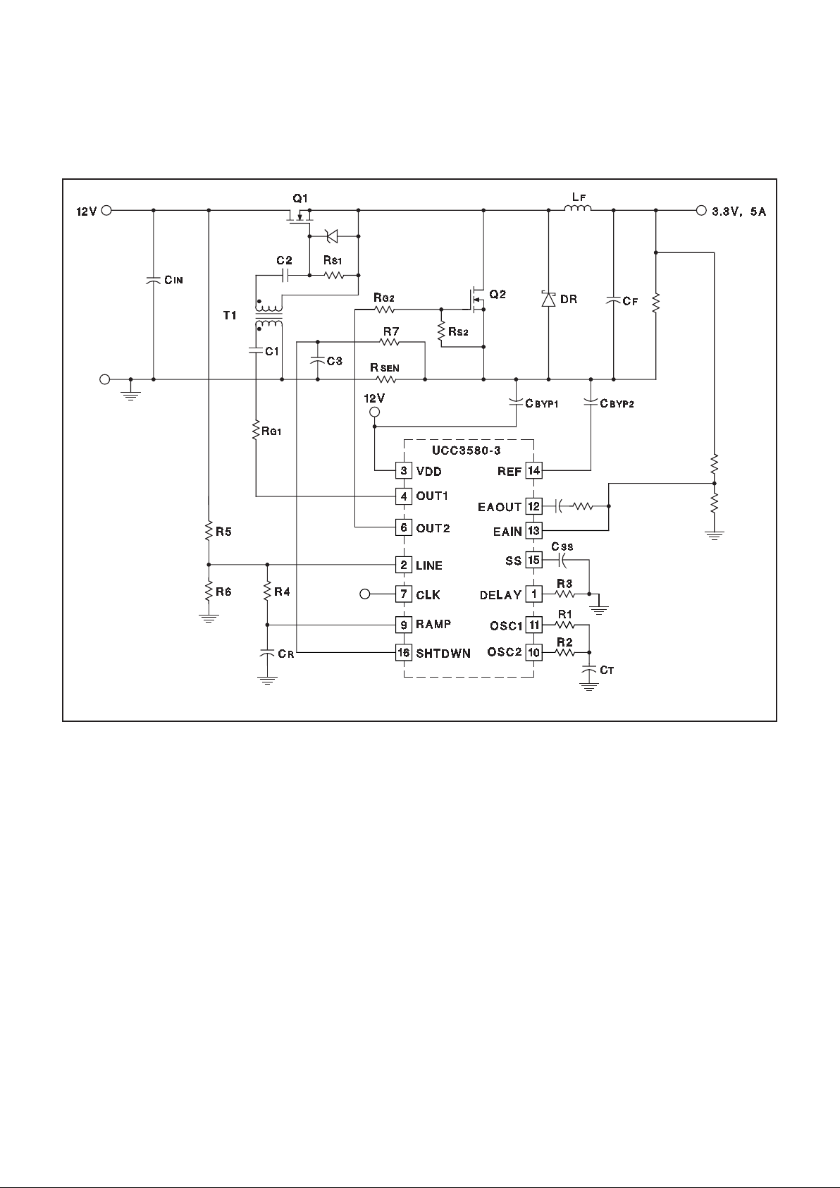
Figure 6. UCC3580 used in a synchronous rectifier application.
APPLICATION INFORMATION (cont.)
UDG-96018-1

IMPORTANT NOTICE
T exas Instruments and its subsidiaries (TI) reserve the right to make changes to their products or to discontinue
any product or service without notice, and advise customers to obtain the latest version of relevant information
to verify, before placing orders, that information being relied on is current and complete. All products are sold
subject to the terms and conditions of sale supplied at the time of order acknowledgement, including those
pertaining to warranty, patent infringement, and limitation of liability.
TI warrants performance of its semiconductor products to the specifications applicable at the time of sale in
accordance with TI’s standard warranty. Testing and other quality control techniques are utilized to the extent
TI deems necessary to support this warranty. Specific testing of all parameters of each device is not necessarily
performed, except those mandated by government requirements.
CERT AIN APPLICATIONS USING SEMICONDUCTOR PRODUCTS MAY INVOLVE POTENTIAL RISKS OF
DEATH, PERSONAL INJURY, OR SEVERE PROPERTY OR ENVIRONMENTAL DAMAGE (“CRITICAL
APPLICATIONS”). TI SEMICONDUCTOR PRODUCTS ARE NOT DESIGNED, AUTHORIZED, OR
WARRANTED TO BE SUITABLE FOR USE IN LIFE-SUPPORT DEVICES OR SYSTEMS OR OTHER
CRITICAL APPLICATIONS. INCLUSION OF TI PRODUCTS IN SUCH APPLICA TIONS IS UNDERSTOOD T O
BE FULLY AT THE CUSTOMER’S RISK.
In order to minimize risks associated with the customer’s applications, adequate design and operating
safeguards must be provided by the customer to minimize inherent or procedural hazards.
TI assumes no liability for applications assistance or customer product design. TI does not warrant or represent
that any license, either express or implied, is granted under any patent right, copyright, mask work right, or other
intellectual property right of TI covering or relating to any combination, machine, or process in which such
semiconductor products or services might be or are used. TI’s publication of information regarding any third
party’s products or services does not constitute TI’s approval, warranty or endorsement thereof.
Copyright 1999, Texas Instruments Incorporated
 Loading...