

Texas Instruments UC5172QTR, UC5172Q, UC5172N Datasheet
Octal Line Driver
INPUTS OUTPUT
EN DATA EIA232E/EIA423A
0 0 5V to 6V
0 1 -5V to -6V
1 X High Z
Note 2: Minimum output swings .
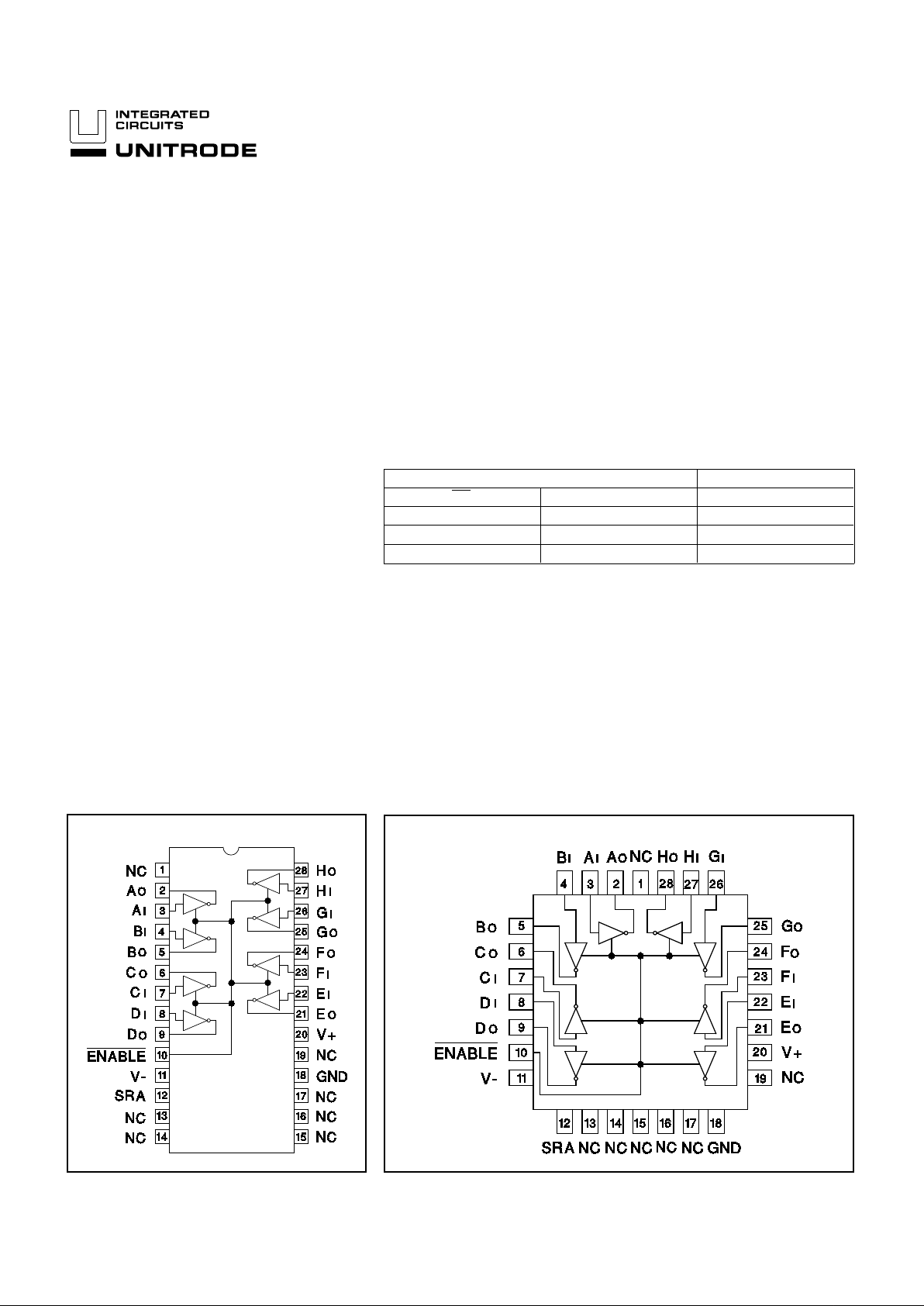
CONNECTION DIAGRAMS
N PACKAGE (TOP VIEW)
Q PACKAGE (TOP VIEW)
V+ (Pin 20) . . . . . . . . . . . . . . . . . . . . . . . . . . . . . . . . . . . . . . . . . . . . . . . . . . 15V
V- (Pin 11). . . . . . . . . . . . . . . . . . . . . . . . . . . . . . . . . . . . . . . . . . . . . . . . . . -15V
PLCC Power Dissipation , TA=25°C (Note 3) . . . . . . . . . . . . . . . . . . . 100 0 mW
DIP Power Dissipat ion, TA=25°C (Note 3) . . . . . . . . . . . . . . . . . . . . . 125 0 mW
Input Voltage . . . . . . . . . . . . . . . . . . . . . . . . . . . . . . . . . . . . . . . . . . -1.5V to +7V
Output Voltage . . . . . . . . . . . . . . . . . . . . . . . . . . . . . . . . . . . . . . . . . -6V to +6V
Slew Rate Resistor . . . . . . . . . . . . . . . . . . . . . . . . . . . . . . . . . . . . . . 2k to 10kΩ
Storage Temperature . . . . . . . . . . . . . . . . . . . . . . . . . . . . . . . -65°C to +150°C
Note 1: All voltages are with respec t to ground, pin 18.
Note 3: Consult Packaging section of Data book for thermal limitat ions and
consideration s of packa ge.
UC5172
The UC5172 is a single-ended octal line driver designed to meet both
standard modem control applications (EIA232E/V.28), and long line
drive applicati ons (EIA423A/V.10/X.26). The slew rate for all 8 drivers
is controlled by a single external resistor. The slew rate and output levels are independent of the power variations.
The UC5172 has high output current, and current balance for long line
drive applicatio ns. EOS - Output parasitic SCRs powered on and off
are 35V, well above signal levels, allowing protection devices to work.
Inputs are compatible TTL+MOS logic families and are diode protected
against negative transients.
• Eight Single-Ended Line Drivers in One
Package
• Meets Standards EIA232E/CCITT V.28,
and EIA423A/CCITT V.10/X.26
• Single External Resistor Controls Slew
Rate
• Wide Supply Voltage Range
• Tri-State Outputs
• Output Short-Circuit Prot ect ion
• Low Power Consumption
• 2kV ESD Protection on all Pins
• EOS on all Output Pins 35V under all
Output Conditions
• High Current Output for Long Line
Drive, Exceeds Standards
FEATURES
ABSOLUTE MAXIMUM RATINGS (Not e 1)
FUNCTIONAL TABLE
9/96
DESCRIPTION

PARAMETER SYMBOL TEST CONDITIONS MIN TYP MAX UNITS
POWER SUPPLY REQUIREMENTS
V+ Range 915V
V- Range -9 -15 V
V+ Supply Current I+ R
L = Infinite En = 0V 15 25 mA
V- Supply Current I- R
L = Infinite En = 0V -17 -25 mA
INPUTS
High-Level Input Voltage V
IH
2.0 V
Low-Level Input Voltage V
IL
0.8 V
Input Clamp Volta ge V
IK II = -15 mA -1.1 -18 V
High Level Input Current I
IH VIH = 2.4V -2 0.25 40 µA
Low Level Input Current I
IL VIL = 0.4V -200 -8.0 µA
OUTPUTS
High Level Output Voltage V
OH VIN = 0.8V RL = Inf. 5.0 5 .3 6 .0 V
EIA232E
En = 0.8V RL = 3k 5.0 5.3 6 . 0 V
(EIA-423A) R
L = 450 4.5 5.2 6.0 V
Low Level Output Volta ge V
OL VIN = 2.0V RL = Inf. -5.0 -5.3 -6.0 V
EIA232E
En = 0.8V RL = 3k -5.0 -5.6 -6.0 V
(EIA-423A) R
L = 450 -4.5 -5.4 -6. 0 V
Output Balance (EIA-4 23A) V
BAL RL = 450, VOH - VOL = VBAL 0.2 0.4 V
Off-Stat e O utput Current I
OZ En = 2.0V, VO =
±
6V, V+ = 15V, V− = -15V -100 100 µA
Short-Circuit Cur re nt I
OS En = 0V VIN = 0V 25 65 mA
V
IN = 5V 25 70 mA
Power Off Output Cur ren t I
PO VO =
±
6V, V+ = V− = 0V -100 100 m A
UC5172
DC ELECTRICAL CHARACTERIST ICS :
AC ELECTRICAL CHARACTERIST ICS :
PARAMETER SYMBOL TEST CONDITIONS MIN TYP MAX UNITS
Output Slew Rate t
R RSRA = 2k 7.6 8.5 9.4 V/µs
t
F RL = 450, CL = 50pF 7.6 8.5 9.4 V/µs
Output Slew Rate t
R RSRA = 10k 1.5 1.7 1.9 Vµs
t
F RL = 450, CL = 50pF 1.5 1.7 1.9 V/µs
Propagation Output
to High Impedance
t
Hz RSRA = 10k 0.8 2.0 µs
t
Lz RL = 450, CL = 50pF 0.5 2.0 µs
Propagation High
Impedance to Output
t
zH RSRA = 10k 2.0 7.0 ms
t
zL RL = 450, CL = 50pF 1.0 7.0 µs
Unless otherwise stat ed these specif ications ho ld for |V+| = |V-| = 10V,
0°C < T
A < +70°C, RSRA = +10k, TA =TJ.
at |V+| = |V-| = +10 V, 0°C < TA < +70°C, TA = TJ.
2
 Loading...