Texas Instruments UC5170CQTR, UC5170CQ, UC5170CN, UC5170CJ Datasheet

UC5170C
FUNCTIONAL TABLE
INPUTS OUTPUTS
HIGH LOW
EN DATA EIA-232E
(2)
EIA423A+EIA232E
0 0 (V+)-3V 5V to 6V
0 1 (V-)-3V −5V to -6V
1 X High Z High Z
Note 2: Minimum output swings.
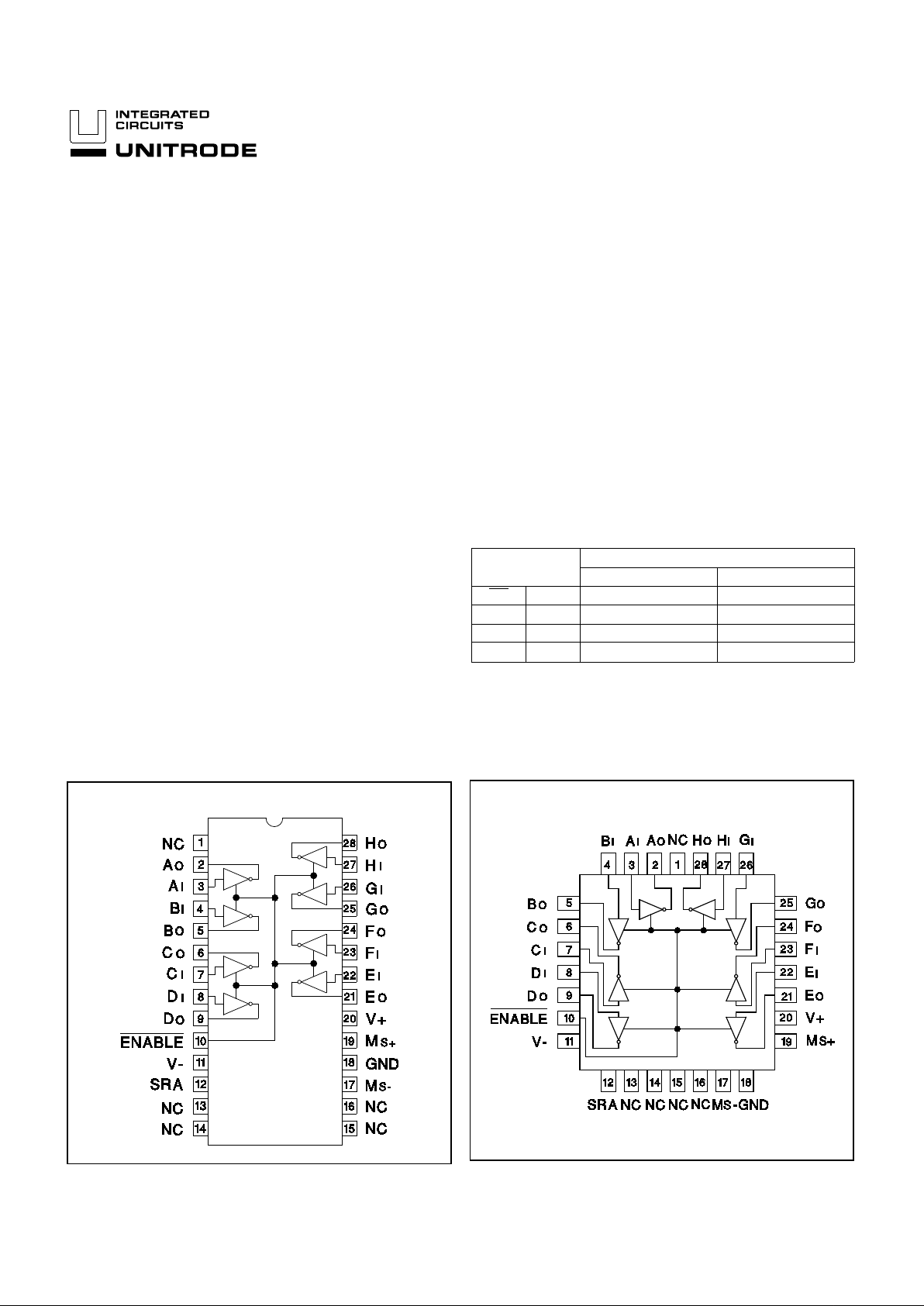
N PACKAGE (TOP VIEW)
Q PACKAGE (TOP VIEW)
Octal Line Driver
FEATURES
• Eight Single Ended Line Drivers in
One Package
• Meets EIA Standards
EIA232E/V.28, EIA423A and
CCITT V.10/X.26
• Single External Resistor Controls
Slew Rate
• Wide Supply Voltage Range
• Tri-State Outputs
• Output Short-Circuit Prot ect ion
DESCRIPTI ON
The UC5170C is a single-ended octal line driver designed to meet both
standard mod em control applicati ons (EIA232E/V.28), and long line drive
applications (EIA423A/V.10/X.26). The slew rate for all eight drivers is controlled by a single external resistor. The slew rate and o utput levels in Low
Mode are independent of the power variations.
Mode selection is easi ly accomplished by taking the select pins (M
S+ and
M
S-) to ground for low output mode (EIA232E/V.28 and EIA423A/V.10) or
to their respective supplies for high mode (EIA232E/V.28). High mode
should only by used to drive adapters that take power from the control
lines, or applications using high threshold receivers.
ABSOLUTE MAXI MUM RATING S (Not e 1)
V+ (Pin 20) . . . . . . . . . . . . . . . . . . . . . . . . . . . . . . . . . . . . . . 15V
V- (Pin 11). . . . . . . . . . . . . . . . . . . . . . . . . . . . . . . . . . . . . . −15V
PLCC Power Dissipation , T
A = 25 ° C (Not e 2 ) . . . . . . 1 000 mW
DIP Power Dissipat ion, T
A = 25°C (Note 2). . . . . . . . 1250 mW
Input Voltag e. . . . . . . . . . . . . . . . . . . . . . . . . . . . . −1.5V t o +7V
Output Voltage . . . . . . . . . . . . . . . . . . . . . . . . . . . −12V to +12V
Slew Rate Resistor. . . . . . . . . . . . . . . . . . . . . . . . . . 2k to 10kΩ
Storage Temperature . . . . . . . . . . . . . . . . . . . −65°C to +150°C
Note 1: All volta ges ar e with respect to ground, pin 18.
Note 2: Consult Packag ing Section of Databoo k for ther mal limitations and considerat ions of pack ages .
CONNECTION DIAGRAMS
7/95

UC5170C
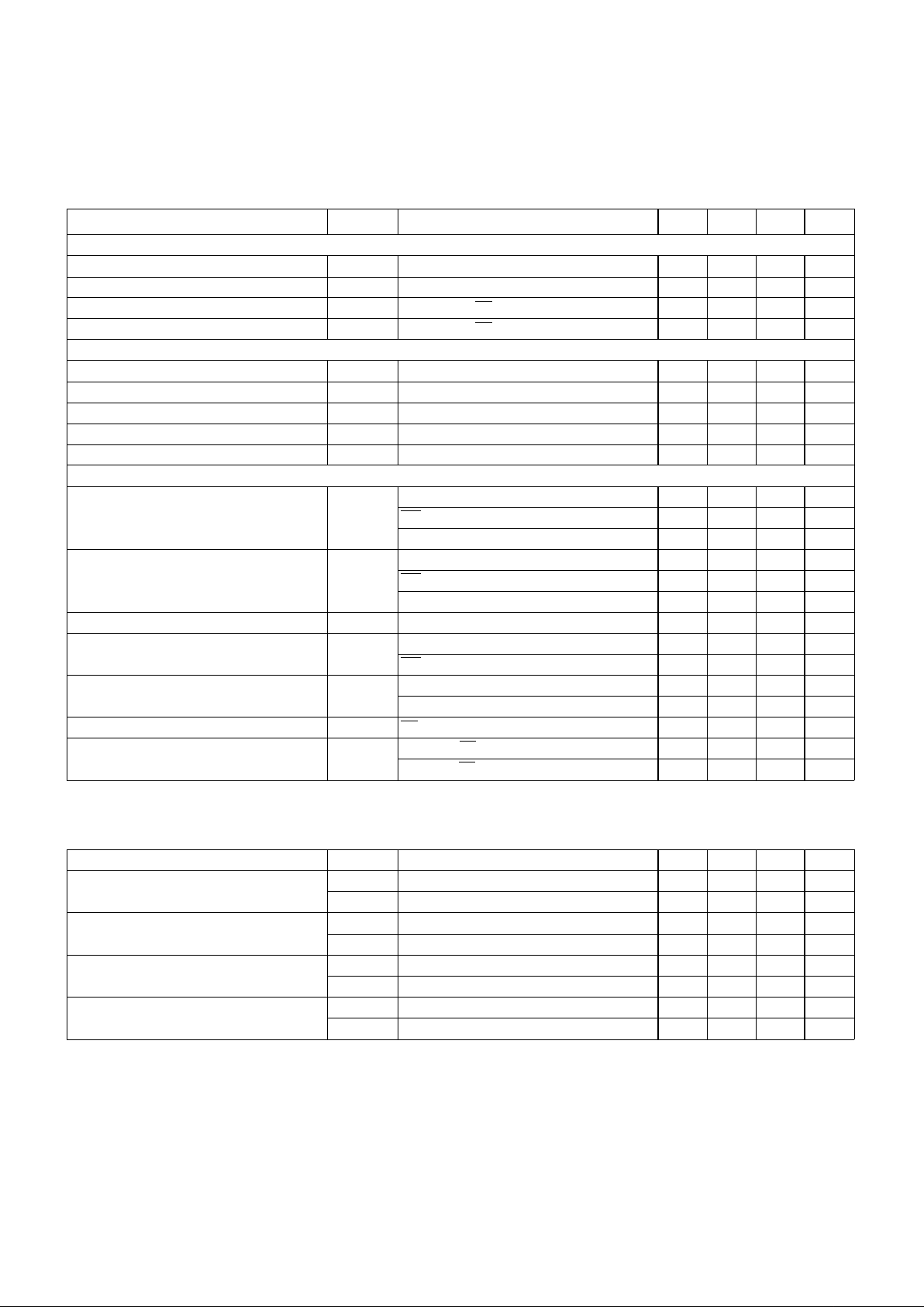
DC ELECTRICAL CHARACTERIST ICS :
PARAMETERS SYMBOL TEST CONDITIONS MIN TYP MAX UNITS
POWER SUPPLY REQUIREMENTS
V+ Range 915V
V- Range -9 -15 V
V+ Supply Current I+ R
L = Infinite En = 0V 25 42 mA
V- Supply Current I- RL = Infinite En = 0V -23 -42 mA
INPUTS
High Level Input Voltage V
IH 2.0 V
Low Level Input Voltage V
IL 0.8 V
Input Clamp Volta ge V
IK II = -15 mA -1.1 -1.8 V
High Level Input Current I
IH VIH = 2.4V 0.25 40 µA
Low Level Input Current I
IL VIL
= 0.4V -200 -8.0 µA
OUTPUTS
High Level (Low Mode) O utput Voltage V
OH VIN = 0.8V RL = Inf. 5.0 5.3 6.0 V
(EIA423A/V.10, EIA232E/V.28)
En = 0.8V RL = 3k 5.0 5.3 6.0 V
R
L = 450 4.5 5.2 6.0 V
Low Level (Low Mode) Output Volt age V
OL VIN = 2.0V RL = Inf. -5.0 -5.3 -6.0 V
(EIA423A/V.10,EIA232E/V.28)
En = 0.8V RL = 3k -5.0 -5.3 -6.0 V
R
L = 450 -4.5 -5.2 -6.0 V
Output Balance (EIA423A/V.10) V
BAL RL = 450 VOH - VOL = V BAL 0.2 0.4 V
High Level (High Mode) Output Volta ge V
OH VIN = 0.8V RL = Inf., MS+ = V+, MS- = V- 7.0 7.6 10 V
(EIA232E/ V.2 8) En = 0.8V RL = 3k, MS+ = V+, MS- = V- 7.0 7.6 10 V
Low Level (High Mode) Output Voltage V
OL VIN = 2.0V RL = Inf. , MS+ = V+, MS- =V- -7.0 -7.7 -10 V
(EIA232E, V.28) En = 0.8V R
L = 3k, MS+ = V+, MS- = V- -7.0 -7.7 -10 V
Off-Stat e O utput Current I
OZ En = 2.0V, VO =
±
6V, V+ = 15V, V- = -15V -100 100 µA
Short-Circuit Cur re nt I
OS VIN = 0V, En = 0V 25 50 mA
V
IN = 5V, En = 0V 25 40 mA
Unless otherwise stated these sp ecif icatio ns hold for | V+ | = | V - | = 10V,
0 < TA < +70°C, MS+ = MS− = 0V, RSRA = +10k, TA =TJ.
at | V+ | = | V - | = 10V, 0 < TA < +70°C, MS+ = MS− = 0V, TA =TJ.
PARAMETERS SYMBOL TEST CONDITIONS MIN TYP MAX UNITS
Output Slew Rate t
R RSRA = 2k 6.65 9 .5 12.3 V/µs
t
F RL = 450, CL = 50pF 6.65 10 12.3 V/µs
Output Slew Rate t
R RSRA = 10k 1.33 1.9 2.45 V/µs
t
F RL = 450, CL = 50pF 1.33 2.2 2.45 V/µs
Propagation Output to t
Hz RSRA = 10k 0.3 1 .0 µs
High Impedance t
Lz RL = 450, CL = 50pF 0. 5 1.0 µs
Propagation High Impedance to t
zH RSRA = 10k 6.0 15 µs
Output t
zL RL = 450, CL = 50pF 7.0 15 µs
AC ELECTRICAL CHARACTERIST ICS :
2
 Loading...