

Page 1

User's Guide
SLUUBM0–May 2017
TPS92518EVM Dual Buck Controller Evaluation Module
This user's guide describes the specifications, board connection description, characteristics, operation,
and use of the combined, two board TPS92518 Evaluation Module (EVM). A complete schematic diagram,
printed circuit board layouts, and bill of materials are included in this document.
Contents
1 Description.................................................................................................................... 2
2 Performance Specifications ................................................................................................ 3
3 Performance Data and Typical Characteristic Curves.................................................................. 4
4 Schematic, PCB Layout, and Bill of Materials.......................................................................... 11
5 Software ..................................................................................................................... 16
6 Use of LEDSPIMCUEVM-879 Microcontroller Board for SPI Communications with the TPS92518............ 22
List of Figures
1 Frequency vs Output Voltage.............................................................................................. 4
2 Efficiency Over Temperature at Different Peak Threshold Settings .................................................. 4
3 PWM Dimming, Multiple PWM Frequencies, Both Channels.......................................................... 5
4 Single-Channel PWM Dimming at 400 Hz ............................................................................... 5
5 SPI Setting Output Enable Bit and Subsequent Switching Initiation.................................................. 6
6 Hardware PWM Enable Pulled High, Triggering Switching ............................................................ 6
7 SPI Clearing Output Enable Bit and Subsequent Switching Shutdown .............................................. 7
8 Hardware PWM Enable Pulled Low, Triggering Chip Shutdown...................................................... 7
9 Current Sharing .............................................................................................................. 8
10 Switch Node Current ........................................................................................................ 8
11 Switch Node Current ........................................................................................................ 9
12 Additional Circuitry Required for Shunt FET Dimming ............................................................... 10
13 TPS92518EVM-878 Schematic .......................................................................................... 11
14 TPS92518EVM-878 Top Side ............................................................................................ 12
15 TPS92518EVM-878 Bottom Side ........................................................................................ 13
16 Setup Screen 1 ............................................................................................................. 16
17 Setup Screen 2 ............................................................................................................. 16
18 Setup Screen 3 ............................................................................................................. 17
19 Setup Screen 4 ............................................................................................................. 17
20 Setup Screen 5 ............................................................................................................. 18
21 Setup Screen 6 ............................................................................................................. 18
22 Setup Screen 7 ............................................................................................................. 19
23 Setup Screen 8 ............................................................................................................. 19
24 Setup Screen 9 ............................................................................................................. 20
25 Setup Screen 10 ........................................................................................................... 20
26 Setup Screen 11 ........................................................................................................... 20
27 LEDSPIMCUEVM-879 Schematic, Page 1............................................................................. 22
28 LEDSPIMCUEVM-879 Schematic, Page 2............................................................................. 23
29 LEDSPIMCUEVM-879 Schematic, Page 3............................................................................. 24
SLUUBM0–May 2017
Submit Documentation Feedback
TPS92518EVM Dual Buck Controller Evaluation Module
Copyright © 2017, Texas Instruments Incorporated
1
Page 2

Description
30 LEDSPIMCUEVM-879 Schematic, Page 4 ............................................................................. 25
List of Tables
1 Connector Descriptions ..................................................................................................... 2
2 Test Points.................................................................................................................... 3
3 TPS92518 EVM Performance Specifications............................................................................ 3
4 TPS92518EVM-878 Bill of Materials..................................................................................... 14
Trademarks
Microsoft, .NET Framework are registered trademarks of Microsoft Corporation.
All other trademarks are the property of their respective owners.
1 Description
The complete two-board TPS92518EVM solution provides a dual-channel, high-brightness LED current
regulator which is configurable via a graphical user interface (GUI). It is designed to operate with an input
voltage in the range of 6.5–65 V. The EVM is setup for default output currents of 538 mA per channel,
easily adjustable to different currents up to 1.65 A, for an LED stack between approximately 3 V to nearly
65 V. The TPS92518 provides high efficiency, high bandwidth, fast PWM dimming, SPI dimming, and
adjustable on-time.
1.1 Typical Applications
This manual outlines the operation and implementation of the TPS92518 as a dual-channel LED current
regulator with the specifications listed in Table 1. For applications with a different input voltage range or
different output voltage range, refer to the TPS92518 data sheet (SLUSCR7). The TPS92518EVM-878
evaluation board is designed to be controlled by a TI microcontroller board, part number
LEDSPIMCUEVM-879, available separately, although it can be controlled by any SPI-capable control
system. Note that the TPS92518x supports a means to enable the part without SPI communication. By
applying a voltage above the second threshold level, 23.6 V typical, on the ENABLE pin, the state of the
LEDxEN register is bypassed. This allows a TPS92518 to be powered and operated using the default
register values (for details, refer to the TPS92518 data sheet (SLUSCR7)).
www.ti.com
1.2 Connector Description
Table 1 describes the connectors and Table 2 lists the test points on the EVM and how to properly
connect, set up, and use the TPS92518EVM-878.
Table 1. Connector Descriptions
Connector Label Description
J1 connects power to channel 1 of the board, and J18 connects power to channel 2.
J1 and J18 VIN, GND
J2 and J3 LED+, LED– and GND
J4 SPI control header
J10 and J11
J12 and J14
SPI control from an
LEDSPIMCUEVM-879
controller board
SPI MISO pullup resistor
jumpers
The evaluation board is set up with both channel supplies connected through R15,
so power connection can be to either J1 or J18 to power both channels from a
single supply. The board silkscreen identifies power (one pin) and ground (two pins)
connections on each connector.
J2 connects the channel 1 output to the LED load, and J3 connects the channel 2
output to a separate LED load. The leads to the LED load should be twisted and
kept short to minimize voltage drop, inductance, and EMI. The board silkscreen
identifies LED+ and LED– and GND.
J4 allows attachment of a header cable for SPI control of the chip. The board
silkscreen identifies GND, MISO, MOSI, SCK, and SSN.
J10 and J11 allow daisy-chaining TPS92518EVM-878 boards to each other with one
LEDSPIMCUEVM-879 control board attached to the left-hand side of the left-most
evaluation board for controlling the TPS92518. This interface allows control of the
chip hardware enable line, PWM inputs to both channels, SPI lines, and hardware
address lines for multiple SSN settings for systems that have multiple
TPS92518EVM-878 boards controlled by a single LEDSPIMCUEVM-879 controller
interface board.
J12 and J14 provide for two different values of pullup resistor to the MISO line, 2.2
kΩ and 4.7 kΩ provided on the evaluation board.
2
TPS92518EVM Dual Buck Controller Evaluation Module
Submit Documentation Feedback
SLUUBM0–May 2017
Copyright © 2017, Texas Instruments Incorporated
Page 3
www.ti.com
Performance Specifications
Table 1. Connector Descriptions (continued)
Connector Label Description
J13 and J15 are jumpers provided to allow for PWM signals to the two channels to
J13 and J15 PWM jumpers
J9
J8 MISO
J7 SPI DI out
J10 Control connector
SSN configuration
jumper
be generated from an LEDSPIMCUEVM-879 (when populated) or applied from an
external source (when jumper is removed and the signal is connected to pin 1 one
of the connector). J13 provides PWM to channel 1 of the chip, while J15 provides
PWM to channel 2.
J9 allows configuration of the SSN chip select line for use with multiple chips on the
same SPI bus.
This jumper enables configurations: shorting pins 5–6 sets the SPI communication
architecture up for a single TPS92518 or the end point of a daisy chain of them,
shorting 1–2 and 5–6 sets up for a TPS92518 in the middle of a daisy-chain, and
shorting 3–4 and 5–6 provides for a star architecture.
If this jumper is closed, it allows multiple TPS92518 devices to be connected in a
star configuration.
This connector allows the TPS92518 board to attach to a microcontroller, such as
the LEDSPIMCUEVM-879.
Table 2. Test Points
Test Point Description
Metal turrets All metal turrets are grounds.
PWM1 and PWM2 The test points labeled PWM1 and PWM2 allow for external signal sources to control the TPS92518
ENABLE The test point labeled ENABLE near J10 allows for an external enable signal to control switching of
VDIGI The VDIGI test point allows for external application of power to the MISO pull-up resistors or
SW1 and SW2 The SW1 and SW2 test points provide locations to monitor the switch nodes of the two channels.
VIN The VIN test point allows for external application of power to the digital system of the chip
hardware PWM dimming.
the TPS92518.
monitoring of the pull-up voltage.
independent of the analog power supplies to either channel 1 or 2. On the evaluation board this is
shorted to the analog supply by R16, so separate application of power is neither necessary nor useful
without removal of R16.
2 Performance Specifications
Table 3. TPS92518 EVM Performance Specifications
Parameter Test Conditions Min Typ Max Units
Input Characteristics
Voltage 6.5 14 65 V
Maximum Input
Current
Output Characteristics
Output Voltage,
V
LED
Output Current,
I
LED
Dimming Methods
Analog LEDx_PKTH_DAC register = 0 to 255 yes
PWM Use PWMx pin input yes
Shunt FET
SLUUBM0–May 2017
Submit Documentation Feedback
Output/LED Voltage (absolute maximum) 0 65
Output/LED Voltage (practical limit) 60
Output current 0 1.65
Default Output Current (Registers = 127/255) 0.538
Use external FET, program LEDx_MAXOFF_DAC register as per
datasheet outline
TPS92518EVM Dual Buck Controller Evaluation Module
Copyright © 2017, Texas Instruments Incorporated
2.5 A
V
A
yes
3
Page 4
Temperature (qC)
Efficiency (%)
Output Current (Amps)
-60 -40 -20 0 20 40 60 80 100 120 140 160
94 0.8
94.1 0.81
94.2 0.82
94.3 0.83
94.4 0.84
94.5 0.85
94.6 0.86
94.7 0.87
94.8 0.88
94.9 0.89
95 0.9
D001
Efficiency
ILED1
ILED2
Output Voltage (V)
Switching Frequency (Hz)
0 5 10 15 20 25 30 35 40 45 50 55
150000
200000
250000
300000
350000
400000
450000
500000
550000
600000
650000
700000
750000
800000
850000
900000
Performance Data and Typical Characteristic Curves
Table 3. TPS92518 EVM Performance Specifications (continued)
Parameter Test Conditions Min Typ Max Units
Systems Characteristics
Switching
frequency
Switching Frequency (fSW) Range 1 2000 kHz
Peak efficiency 95 %
Operating
temperature
3 Performance Data and Typical Characteristic Curves
Figure 1 through Figure 4 illustrate the performance data and typical characteristic curves.
www.ti.com
–40 25 125 ºC
Conditions: VIN50 V, peak threshold = 50, minimum off-time = 127
4
Conditions:IN50 V, V
Figure 2. Efficiency Over Temperature at Different Peak Threshold Settings
TPS92518EVM Dual Buck Controller Evaluation Module
24.7 V, peak threshold = 120, minimum off-time = 127
LED
Figure 1. Frequency vs Output Voltage
Copyright © 2017, Texas Instruments Incorporated
Submit Documentation Feedback
SLUUBM0–May 2017
Page 5
Dutycycle (%)
Output Current (A)
0 10 20 30 40 50 60 70 80 90 100
0
0.05
0.1
0.15
0.2
0.25
0.3
0.35
0.4
0.45
0.5
Ch. 2, PWMfreq=400Hz
Dutycycle (%)
Output Current (A)
0 10 20 30 40 50 60 70 80 90 100
0
0.05
0.1
0.15
0.2
0.25
0.3
0.35
0.4
0.45
0.5
Ch. 1 PWMfreq=250Hz
Ch. 2 PWMfreq=250Hz
Ch. 1 PWMfreq= 400Hz
Ch. 2 PWMfreq=400Hz
Ch. 1 PWMfreq=600Hz
Ch. 2 PWMfreq=600Hz
Ch. 1 PWMfreq=1000Hz
Ch. 2 PWMfreq=1000Hz
www.ti.com
Performance Data and Typical Characteristic Curves
VIN12 V, V
VIN12 V, V
3 V, peak threshold = 127, off time = 127
LED
Figure 3. PWM Dimming, Multiple PWM Frequencies, Both Channels
3 V, peak threshold = 127, off time = 127
LED
Figure 4. Single-Channel PWM Dimming at 400 Hz
SLUUBM0–May 2017
Submit Documentation Feedback
TPS92518EVM Dual Buck Controller Evaluation Module
Copyright © 2017, Texas Instruments Incorporated
5
Page 6
Performance Data and Typical Characteristic Curves
3.1 Startup Waveforms
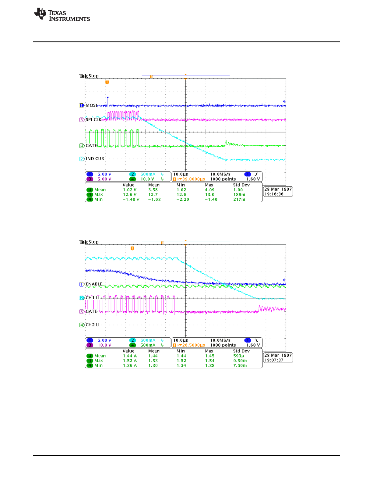
3.1.1 Startup After SPI Enable Command
Figure 5. SPI Setting Output Enable Bit and Subsequent Switching Initiation
www.ti.com
3.1.2 Startup on Hardware Enable Pin Transition
Figure 6. Hardware PWM Enable Pulled High, Triggering Switching
6
TPS92518EVM Dual Buck Controller Evaluation Module
Copyright © 2017, Texas Instruments Incorporated
Submit Documentation Feedback
SLUUBM0–May 2017
Page 7
www.ti.com
3.2 Shutdown Waveforms
3.2.1 Shutdown After SPI Disable
Figure 7. SPI Clearing Output Enable Bit and Subsequent Switching Shutdown
Performance Data and Typical Characteristic Curves
3.2.2 Shutdown After Hardware Enable Pin Transition
Figure 8. Hardware PWM Enable Pulled Low, Triggering Chip Shutdown
SLUUBM0–May 2017
Submit Documentation Feedback
TPS92518EVM Dual Buck Controller Evaluation Module
Copyright © 2017, Texas Instruments Incorporated
7
Page 8
Performance Data and Typical Characteristic Curves
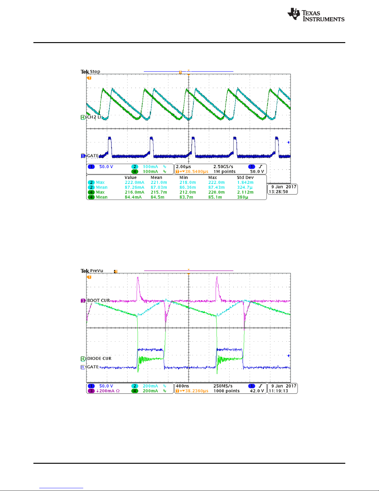
3.3 Current Sharing
The TPS92518 device can be set up to share current with both channels driving a single load.
www.ti.com
VIN= 65 V, driving 1 LED for a V
current, showing max and mean inductor currents on channels 1 and 2
of 3.0062 V, with a peak threshold = 45 to get approximately a 225-mA LED
LED
Figure 9. Current Sharing
3.4 Diode and Boot Capacitor Current
3.4.1 Diode, Inductor, and Boot Capacitor Current at Low Output Current
Showing inductor current into the LED and current flow through the catch diode and boot capacitor used for supplying
gate drive power. VIN= 65 V, V
8
TPS92518EVM Dual Buck Controller Evaluation Module
= 23 V, T
LED
register setting = 50, peak threshold register setting = 1
OFF
Figure 10. Switch Node Current
Copyright © 2017, Texas Instruments Incorporated
Submit Documentation Feedback
SLUUBM0–May 2017
Page 9
www.ti.com
Performance Data and Typical Characteristic Curves
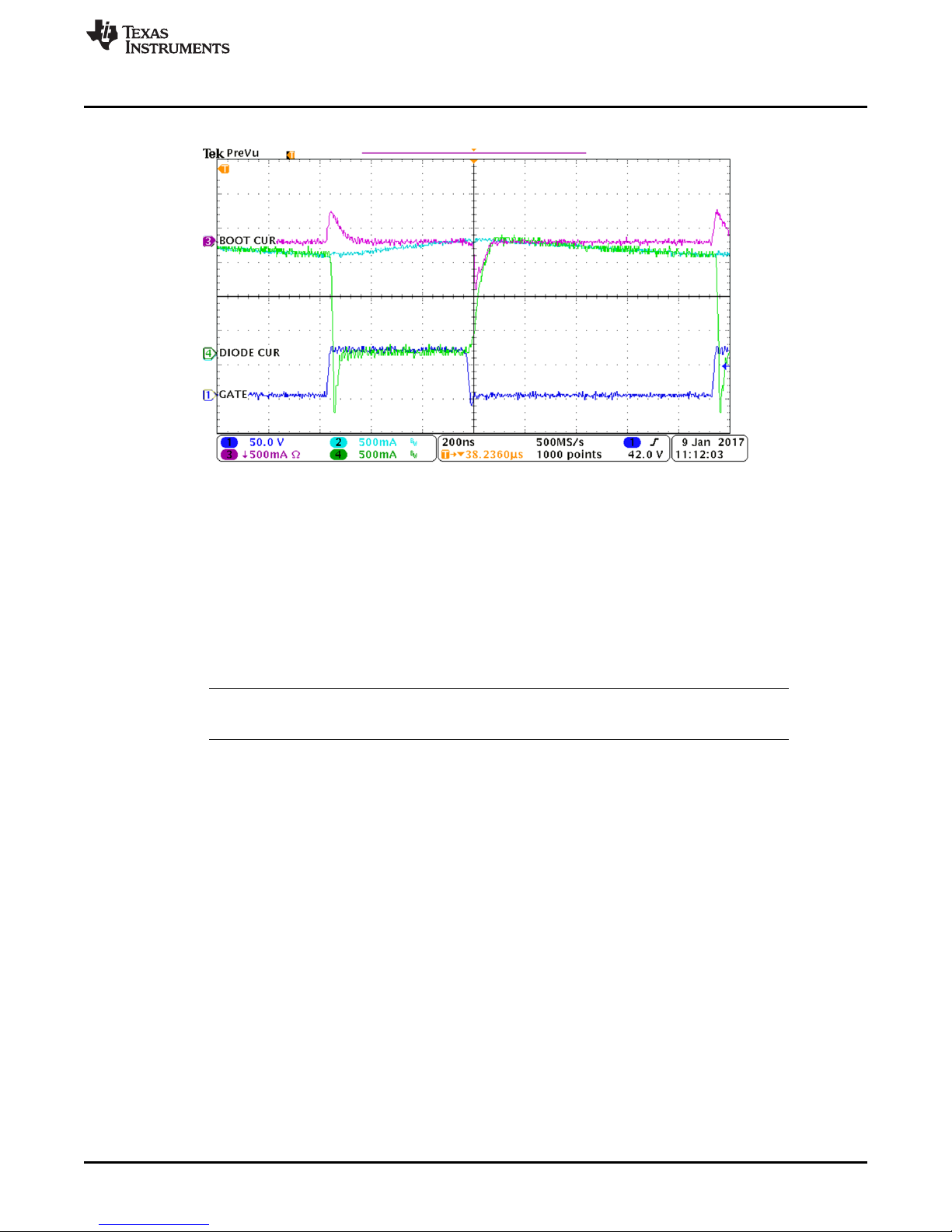
3.4.2 Diode, Inductor, and Boot Capacitor Current at High Output Current
Showing inductor current into the LED and current flow through the catch diode and boot capacitor used for supplying
gate drive power. VIN= 65 V, V
= 23 V, T
LED
register setting 50, peak threshold register setting = 1
OFF
Figure 11. Switch Node Current
3.4.3 Shunt FET Dimming
Shunt FET dimming is simple with the TPS92518. Short leads between the evaluation board and the LED
load boards are important to prevent V
board also helps to reduce V
overshoot. Adding an appropriately rated diode from the LED+ line that
LED
overshoot. Locating the shunt FET on or near the LED load
LED
conducts back to the positive VINinput will clamp voltage overshoot.
NOTE: There is no provision for mounting such a diode on the board: it must be soldered into the
wiring used to connect the shunt FET into the circuit.
Similarly, repopulating R17 and C21 with different values will also protect the V
pin from overshoots.
LED
Figure 12 illustrates the circuitry modifications for shunt FET dimming: increasing the size of R17, adding
a diode to VIN, and adding an appropriately-rated FET with a gate pulldown resistor. Either adding a diode
or increasing R17 should be adequate. While the modified schematic shows both output capacitors
removed, replacing one with a 220-pF capacitor rather than just removing both may give better V
overshoot performance.
LED
SLUUBM0–May 2017
Submit Documentation Feedback
TPS92518EVM Dual Buck Controller Evaluation Module
Copyright © 2017, Texas Instruments Incorporated
9
Page 10

Performance Data and Typical Characteristic Curves
www.ti.com
Figure 12. Additional Circuitry Required for Shunt FET Dimming
3.4.4 Undervoltage Lockout Description
The TPS92518 can be set up with undervoltage lockout protection with the ability to change the turn-on
threshold and hysteresis, by populating a resistive divider that is unpopulated on the evaluation board.
This involves loading R1 and changing the value of R2, and possibly populating C28. For details refer to
the TPS92518 data sheet (SLUSCR7).
10
TPS92518EVM Dual Buck Controller Evaluation Module
Copyright © 2017, Texas Instruments Incorporated
Submit Documentation Feedback
SLUUBM0–May 2017
Page 11

www.ti.com
Schematic, PCB Layout, and Bill of Materials
11
SLUUBM0– May 2017
Submit Documentation Feedback
Copyright © 2017, Texas Instruments Incorporated
TPS92518EVM Dual Buck Controller Evaluation Module
4 Schematic, PCB Layout, and Bill of Materials
This section contains TPS92518EVM-878 schematics, PCB layouts, and bill of materials (BOM).
4.1 Schematic
Figure 13 illustrates the TPS92518EVM-878 schematic.
Figure 13. TPS92518EVM-878 Schematic
Page 12

Schematic, PCB Layout, and Bill of Materials
4.2 Layout
Figure 14 and Figure 15 illustrate the top and bottom side TPS92518EVM-878 PCB layouts.
www.ti.com
12
TPS92518EVM Dual Buck Controller Evaluation Module
Figure 14. TPS92518EVM-878 Top Side
Copyright © 2017, Texas Instruments Incorporated
Submit Documentation Feedback
SLUUBM0–May 2017
Page 13

www.ti.com
Schematic, PCB Layout, and Bill of Materials
Figure 15. TPS92518EVM-878 Bottom Side
SLUUBM0–May 2017
Submit Documentation Feedback
TPS92518EVM Dual Buck Controller Evaluation Module
Copyright © 2017, Texas Instruments Incorporated
13
Page 14

Schematic, PCB Layout, and Bill of Materials
www.ti.com
14
SLUUBM0– May 2017
Submit Documentation Feedback
Copyright © 2017, Texas Instruments Incorporated
TPS92518EVM Dual Buck Controller Evaluation Module
4.3 Bill of Materials
Table 4 lists the TPS92518EVM-878 BOM.
Table 4. TPS92518EVM-878 Bill of Materials
Designator Qty Value Description Package Reference Part Number Manufacturer
(none) 1 Printed Circuit Board PWR878 Any
C2, C3, C4, C5, C6, C7, C8,
C9, C22, C23, C27
11 2.2uF CAP, CERM, 2.2 µF, 100 V, ±10%, X7R, AEC-Q200 Grade 1, CGA6N3X7R2A225K230AB TDK
C10, C13 2 0.1uF CAP, CERM, 0.1 µF, 16 V, ±10%, X7R, 0603 0603 GCM188R71C104KA37D Murata
C11, C12 2 2.2uF CAP, CERM, 2.2 µF, 16 V, ±10%, X7R, 0805 0805 GCM21BR71C225KA64L Murata
C14, C15, C17, C18 4 1uF CAP, CERM, 1 µF, 100 V, ±10%, X7R, 1206 1206 GCM31CR72A105KA03L Murata
D1, D2 2 100V Diode, Switching, 100 V, 0.2 A, SOD-123 SOD-123 MMSD4148T1G ON Semiconductor
D3, D4 2 100V Diode, Schottky, 100 V, 3 A, SMC SMC SS3H10HE3_A/I Vishay-Siliconix
D5 1 100V Diode, Schottky, 100 V, 0.25 A, SOD-323F SOD-323F BAT46WJ,115 NXP Semiconductor
H1, H2, H3, H4 4 Bumpon, Hemisphere, 0.44 X 0.20, Clear Transparent Bumpon SJ-5303 (CLEAR) 3M
J1, J5 2 Header, 2.54 mm, 3x1, TH Header, 2.54mm, 3x1, TH 22-11-2032 Molex
J2, J3 2 Header, 2.54mm, 2x1, Vertical, TH Header, 2.54mm, 2x1, TH 22-23-2021 Molex
J4 1 Header, 100mil, 5x1, Gold, TH 5x1 Header TSW-105-07-G-S Samtec
J6, J7, J12, J13, J14 5 Header, 100mil, 2x1, Gold, TH 2x1 Header TSW-102-07-G-S Samtec
J8 1 Header, 100mil, 3x2, Gold, TH 3x2 Header TSW-103-07-G-D Samtec
J9 1 Header, 100mil, 4x2, Gold, TH 4x2 Header TSW-104-07-G-D Samtec
J10 1 Header, 2.54mm, 10x2, Tin, R/A, TH Header, 2.54mm, 10x2, R/A,THTSW-110-08-T-D-RA Samtec
J11 1 Receptacle, 2.54mm, 10x2, Gold, R/A, TH Receptacle, 2.54mm, 10x2,
R/A, TH
SSW-110-02-G-D-RA Samtec
L1, L2 2 100uH Inductor, Shielded, Ferrite, 100 µH, 2 A, 0.108 ohm, AEC-Q200 Grade
0, SMD
12.8x12.5mm MDH12577C-101MA=P3 Murata
Q1, Q2 2 100V MOSFET, N-CH, 100 V, 20 A, AEC-Q101, 8-PowerVDFN 8-PowerVDFN STL8N10LF3 STMicroelectronics
R2 1 20.0k RES, 20.0 k, 1%, 0.125 W, 0805 0805 CRCW080520K0FKEA Vishay-Dale
R7, R8 2 0.15 RES, 0.15 ohm, 1%, 1/2W, 1206 1206 (3216 Metric) ERJ-8BSFR15V Panasonic Electronic
Components
R10, R16, R17 3 0 RES, 0, 5%, 0.1 W, 0603 0603 CRCW06030000Z0EA Vishay-Dale
R11 1 2.2 kΩ RES, 2.2 k, 5%, 0.1 W, 0603 0603 CRCW06032K20JNEA Vishay-Dale
R12 1 4.7k RES, 4.7 k, 5%, 0.1 W, 0603 0603 CRCW06034K70JNEA Vishay-Dale
R13, R14 2 4.75 RES, 4.75, 1%, 0.1 W, 0603 0603 CRCW06034R75FKEA Vishay-Dale
R15 1 0 RES, 0, 5%, 0.25 W, 1206 1206 CRCW12060000Z0EA Vishay-Dale
SH-J6, SH-J8, SH-J9, SH-
J12, SH-J13
5 Shunt, 2.54mm, Gold, Black Shunt, 2.54mm, Black 60900213421 Wurth Elektronik
TP1, TP2, TP3, TP4, TP5,
TP6, TP7
7 Orange Test Point, Compact, Orange, TH Orange Compact Testpoint 5008 Keystone
Page 15

www.ti.com
Schematic, PCB Layout, and Bill of Materials
15
SLUUBM0– May 2017
Submit Documentation Feedback
Copyright © 2017, Texas Instruments Incorporated
TPS92518EVM Dual Buck Controller Evaluation Module
Table 4. TPS92518EVM-878 Bill of Materials (continued)
Designator Qty Value Description Package Reference Part Number Manufacturer
TP8, TP9, TP10, TP11,
TP12, TP13, TP14, TP15
8 Double Terminal, Turret, TH, Double Keystone1502-2 1502-2 Keystone
U1 1 65V Automotive Dual Buck LED Controller with SPI Interface,
PWP0024J (TSSOP-24)
PWP0024J TPS92518QPWPRQ1 Texas Instruments
C1, C16, C21, C25, C26 0 0.1uF CAP, CERM, 0.1 µF, 16 V, ±10%, X7R, 0603 0603 GCM188R71C104KA37D Murata
C19, C20 0 0.01uF CAP, CERM, 0.01 µF, 100 V, ±10%, X7R, 0603 0603 GCM188R72A103KA37D Murata
FID1, FID2, FID3 0 Fiducialmark. There is nothing to buy or mount. Fiducial N/A N/A
R1 0 80.6k RES, 80.6 k, 1%, 0.1 W, 0603 0603 CRCW060380K6FKEA Vishay-Dale
R3, R4 0 1.00k RES, 1.00 k, 1%, 0.125 W, 0805 0805 CRCW08051K00FKEA Vishay-Dale
R5 0 0 RES, 0, 5%, 0.1 W, 0603 0603 CRCW06030000Z0EA Vishay-Dale
Page 16

Software
5 Software
5.1 TPS92518 Demonstration Kit Software Installation
Double-click on TPS92518 Demonstration Kit Installer.exe and click ‘yes’ when Windows Account Control
asks to allow the program to make changes to the computer.
This will bring up the evaluation software screen:
www.ti.com
Click the Next > button to install.
Click the Next > button.
Figure 16. Setup Screen 1
Figure 17. Setup Screen 2
16
TPS92518EVM Dual Buck Controller Evaluation Module
Copyright © 2017, Texas Instruments Incorporated
Submit Documentation Feedback
SLUUBM0–May 2017
Page 17

www.ti.com
Click the Next > button.
Software
Figure 18. Setup Screen 3
Wait for it to finish extracting and installing files.
SLUUBM0–May 2017
Submit Documentation Feedback
Figure 19. Setup Screen 4
TPS92518EVM Dual Buck Controller Evaluation Module
Copyright © 2017, Texas Instruments Incorporated
17
Page 18

Software
Figure 20. Setup Screen 5
Check the box stating you accept the license terms and click the Install > button.
www.ti.com
It may be necessary to stop other programs using Microsoft®.NET Framework®during the installation
process. Select Yes, if asked.
18
TPS92518EVM Dual Buck Controller Evaluation Module
Figure 21. Setup Screen 6
Copyright © 2017, Texas Instruments Incorporated
Submit Documentation Feedback
SLUUBM0–May 2017
Page 19

www.ti.com
Software
Figure 22. Setup Screen 7
Wait for .NET to download, verify, and install.
SLUUBM0–May 2017
Submit Documentation Feedback
Figure 23. Setup Screen 8
TPS92518EVM Dual Buck Controller Evaluation Module
Copyright © 2017, Texas Instruments Incorporated
19
Page 20

Software
Click the Finish > button.
www.ti.com
Figure 24. Setup Screen 9
Figure 25. Setup Screen 10
Restart your computer by clicking on the Restart Now button.
Figure 26. Setup Screen 11
Click on the Finish > button.
At this point the software should be ready to use. Click on the TI TPS92518 Demonstration Kit icon.
20
TPS92518EVM Dual Buck Controller Evaluation Module
Copyright © 2017, Texas Instruments Incorporated
Submit Documentation Feedback
SLUUBM0–May 2017
Page 21

www.ti.com
Quick Start: Provide input power of 6.5 V to 65 V to VIN, provide LED loads with output voltages of
between 2 V and 64 V to the two output channels. Next click on the TPS92518 Enabled box so it is
checked, then on the Buck 1 Enable: and Buck 2 Enable: boxes so they are checked. The integrated
circuit should start switching on each channel and regulating current to the LED loads.
Design Customization and GUI Operation: Access to key TPS92518 registers is provided via the GUI
main window. Each channel Peak Threshold, Off Time and Maximum Off-time can be adjusted using
the respective slider. Minimum limits are enforced in the GUI for the Off-Time and Maximum Off-time as
these values should not be set <10 except under specific and controlled conditions. (see the datasheet
section: Off-Time Thresholds - LEDx_TOFF_DAC and LEDx_MAXOFF_DAC) The registers can still be set
manually to lower values via the SPI Command section of the GUI. The sliders can be moved and the
affect on the output current and switching frequency observed.
For a specific design configuration, the Design Tool button can be selected. This opens a simple
TPS92518 design calculator window. Design Parameters can be entered and adjusted. Component and
register values will be calculated. This calculator can be used to aid in any TPS92518 design, and is not
just for use with the EVM.
For each slider adjustment an estimation of the relevant parameter value is also shown. For the peak
current estimate, the value of the sense resistor can be set in the area below the sliders. (default is the
actual EVM value of 0.15 Ohms) The estimated off-time and maximum off-times are also updated and
reflect the current LED output voltage as measured by the TPS92518x internal ADC.
In the GUI Control section, the TPS92518 enable pin voltage can be controlled via the enable check box.
The GUI also provides the ability to create PWM dimming signals. A PWM duty cycle and frequency can
be set creating the corresponding signal at the TPS92518 PWMx pin. In normal operation the PWM duty
cycle must be left at 100% to disable PWM dimming.
Registers may also be written manually via the SPI Command section. By using the TPS92518 datasheet
Registers section as a guide, specific registers can be manually read and written. To preform a register
write, set the write check-box. Un-check the box for a read. When reading and writing manually it is best
to disable the Auto Refresh of the registers by toggling the feature via the 'Auto Refresh' box. Once the
register value and write data (if applicable) are set, select the Send Command button. Due to the nature of
a SPI bus operation, read commands must be sent twice; once to load the read command and another
time to clock out the requested data.
Software
SLUUBM0–May 2017
Submit Documentation Feedback
TPS92518EVM Dual Buck Controller Evaluation Module
Copyright © 2017, Texas Instruments Incorporated
21
Page 22

Use of LEDSPIMCUEVM-879 Microcontroller Board for SPI Communications with the TPS92518
www.ti.com
6 Use of LEDSPIMCUEVM-879 Microcontroller Board for SPI Communications with the
TPS92518
The LEDSPIMCUEVM-879 evaluation board is available separately to be used with TI's TPS92518 Bench
Evaluation Software. It comes with firmware installed that converts the software settings into SPI and
hardware-generated PWM signals to drive the TPS92518. It is set up correctly as packaged, but make
sure that jumpers J6, J7, J8, and J9 are all shorted. These provide the power for the SPI pullup hardware,
the PWM signals, and the enable signal to the TPS92518. Reprogramming the LEDSPIMCUEVM-879 is
beyond the scope of this document, and firmware for reflashing the existing board is not supplied. The
board has DC isolation between the USB section and the TPS92518 driver section, and voltage
translators to handle the I/O logic level requirements of the TPS92518. Schematics are supplied as a
guide to determining if the microcontroller board has been damaged and is not communicating correctly
with the TPS92518 evaluation board.
Figure 27. LEDSPIMCUEVM-879 Schematic, Page 1
22
TPS92518EVM Dual Buck Controller Evaluation Module
Copyright © 2017, Texas Instruments Incorporated
Submit Documentation Feedback
SLUUBM0–May 2017
Page 23

www.ti.com
Use of LEDSPIMCUEVM-879 Microcontroller Board for SPI Communications with the TPS92518
Figure 28. LEDSPIMCUEVM-879 Schematic, Page 2
SLUUBM0–May 2017
Submit Documentation Feedback
TPS92518EVM Dual Buck Controller Evaluation Module
Copyright © 2017, Texas Instruments Incorporated
23
Page 24

Use of LEDSPIMCUEVM-879 Microcontroller Board for SPI Communications with the TPS92518
www.ti.com
Figure 29. LEDSPIMCUEVM-879 Schematic, Page 3
24
TPS92518EVM Dual Buck Controller Evaluation Module
Copyright © 2017, Texas Instruments Incorporated
Submit Documentation Feedback
SLUUBM0–May 2017
Page 25

www.ti.com
Use of LEDSPIMCUEVM-879 Microcontroller Board for SPI Communications with the TPS92518
Figure 30. LEDSPIMCUEVM-879 Schematic, Page 4
SLUUBM0–May 2017
Submit Documentation Feedback
TPS92518EVM Dual Buck Controller Evaluation Module
Copyright © 2017, Texas Instruments Incorporated
25
Page 26

STANDARD TERMS FOR EVALUATION MODULES
1. Delivery: TI delivers TI evaluation boards, kits, or modules, including any accompanying demonstration software, components, and/or
documentation which may be provided together or separately (collectively, an “EVM” or “EVMs”) to the User (“User”) in accordance
with the terms set forth herein. User's acceptance of the EVM is expressly subject to the following terms.
1.1 EVMs are intended solely for product or software developers for use in a research and development setting to facilitate feasibility
evaluation, experimentation, or scientific analysis of TI semiconductors products. EVMs have no direct function and are not
finished products. EVMs shall not be directly or indirectly assembled as a part or subassembly in any finished product. For
clarification, any software or software tools provided with the EVM (“Software”) shall not be subject to the terms and conditions
set forth herein but rather shall be subject to the applicable terms that accompany such Software
1.2 EVMs are not intended for consumer or household use. EVMs may not be sold, sublicensed, leased, rented, loaned, assigned,
or otherwise distributed for commercial purposes by Users, in whole or in part, or used in any finished product or production
system.
2 Limited Warranty and Related Remedies/Disclaimers:
2.1 These terms do not apply to Software. The warranty, if any, for Software is covered in the applicable Software License
Agreement.
2.2 TI warrants that the TI EVM will conform to TI's published specifications for ninety (90) days after the date TI delivers such EVM
to User. Notwithstanding the foregoing, TI shall not be liable for a nonconforming EVM if (a) the nonconformity was caused by
neglect, misuse or mistreatment by an entity other than TI, including improper installation or testing, or for any EVMs that have
been altered or modified in any way by an entity other than TI, (b) the nonconformity resulted from User's design, specifications
or instructions for such EVMs or improper system design, or (c) User has not paid on time. Testing and other quality control
techniques are used to the extent TI deems necessary. TI does not test all parameters of each EVM.
User's claims against TI under this Section 2 are void if User fails to notify TI of any apparent defects in the EVMs within ten (10)
business days after delivery, or of any hidden defects with ten (10) business days after the defect has been detected.
2.3 TI's sole liability shall be at its option to repair or replace EVMs that fail to conform to the warranty set forth above, or credit
User's account for such EVM. TI's liability under this warranty shall be limited to EVMs that are returned during the warranty
period to the address designated by TI and that are determined by TI not to conform to such warranty. If TI elects to repair or
replace such EVM, TI shall have a reasonable time to repair such EVM or provide replacements. Repaired EVMs shall be
warranted for the remainder of the original warranty period. Replaced EVMs shall be warranted for a new full ninety (90) day
warranty period.
3 Regulatory Notices:
3.1 United States
3.1.1 Notice applicable to EVMs not FCC-Approved:
FCC NOTICE: This kit is designed to allow product developers to evaluate electronic components, circuitry, or software
associated with the kit to determine whether to incorporate such items in a finished product and software developers to write
software applications for use with the end product. This kit is not a finished product and when assembled may not be resold or
otherwise marketed unless all required FCC equipment authorizations are first obtained. Operation is subject to the condition
that this product not cause harmful interference to licensed radio stations and that this product accept harmful interference.
Unless the assembled kit is designed to operate under part 15, part 18 or part 95 of this chapter, the operator of the kit must
operate under the authority of an FCC license holder or must secure an experimental authorization under part 5 of this chapter.
3.1.2 For EVMs annotated as FCC – FEDERAL COMMUNICATIONS COMMISSION Part 15 Compliant:
CAUTION
This device complies with part 15 of the FCC Rules. Operation is subject to the following two conditions: (1) This device may not
cause harmful interference, and (2) this device must accept any interference received, including interference that may cause
undesired operation.
Changes or modifications not expressly approved by the party responsible for compliance could void the user's authority to
operate the equipment.
FCC Interference Statement for Class A EVM devices
NOTE: This equipment has been tested and found to comply with the limits for a Class A digital device, pursuant to part 15 of
the FCC Rules. These limits are designed to provide reasonable protection against harmful interference when the equipment is
operated in a commercial environment. This equipment generates, uses, and can radiate radio frequency energy and, if not
installed and used in accordance with the instruction manual, may cause harmful interference to radio communications.
Operation of this equipment in a residential area is likely to cause harmful interference in which case the user will be required to
correct the interference at his own expense.
Page 27

FCC Interference Statement for Class B EVM devices
NOTE: This equipment has been tested and found to comply with the limits for a Class B digital device, pursuant to part 15 of
the FCC Rules. These limits are designed to provide reasonable protection against harmful interference in a residential
installation. This equipment generates, uses and can radiate radio frequency energy and, if not installed and used in accordance
with the instructions, may cause harmful interference to radio communications. However, there is no guarantee that interference
will not occur in a particular installation. If this equipment does cause harmful interference to radio or television reception, which
can be determined by turning the equipment off and on, the user is encouraged to try to correct the interference by one or more
of the following measures:
• Reorient or relocate the receiving antenna.
• Increase the separation between the equipment and receiver.
• Connect the equipment into an outlet on a circuit different from that to which the receiver is connected.
• Consult the dealer or an experienced radio/TV technician for help.
3.2 Canada
3.2.1 For EVMs issued with an Industry Canada Certificate of Conformance to RSS-210 or RSS-247
Concerning EVMs Including Radio Transmitters:
This device complies with Industry Canada license-exempt RSSs. Operation is subject to the following two conditions:
(1) this device may not cause interference, and (2) this device must accept any interference, including interference that may
cause undesired operation of the device.
Concernant les EVMs avec appareils radio:
Le présent appareil est conforme aux CNR d'Industrie Canada applicables aux appareils radio exempts de licence. L'exploitation
est autorisée aux deux conditions suivantes: (1) l'appareil ne doit pas produire de brouillage, et (2) l'utilisateur de l'appareil doit
accepter tout brouillage radioélectrique subi, même si le brouillage est susceptible d'en compromettre le fonctionnement.
Concerning EVMs Including Detachable Antennas:
Under Industry Canada regulations, this radio transmitter may only operate using an antenna of a type and maximum (or lesser)
gain approved for the transmitter by Industry Canada. To reduce potential radio interference to other users, the antenna type
and its gain should be so chosen that the equivalent isotropically radiated power (e.i.r.p.) is not more than that necessary for
successful communication. This radio transmitter has been approved by Industry Canada to operate with the antenna types
listed in the user guide with the maximum permissible gain and required antenna impedance for each antenna type indicated.
Antenna types not included in this list, having a gain greater than the maximum gain indicated for that type, are strictly prohibited
for use with this device.
Concernant les EVMs avec antennes détachables
Conformément à la réglementation d'Industrie Canada, le présent émetteur radio peut fonctionner avec une antenne d'un type et
d'un gain maximal (ou inférieur) approuvé pour l'émetteur par Industrie Canada. Dans le but de réduire les risques de brouillage
radioélectrique à l'intention des autres utilisateurs, il faut choisir le type d'antenne et son gain de sorte que la puissance isotrope
rayonnée équivalente (p.i.r.e.) ne dépasse pas l'intensité nécessaire à l'établissement d'une communication satisfaisante. Le
présent émetteur radio a été approuvé par Industrie Canada pour fonctionner avec les types d'antenne énumérés dans le
manuel d’usage et ayant un gain admissible maximal et l'impédance requise pour chaque type d'antenne. Les types d'antenne
non inclus dans cette liste, ou dont le gain est supérieur au gain maximal indiqué, sont strictement interdits pour l'exploitation de
l'émetteur
3.3 Japan
3.3.1 Notice for EVMs delivered in Japan: Please see http://www.tij.co.jp/lsds/ti_ja/general/eStore/notice_01.page 日本国内に
輸入される評価用キット、ボードについては、次のところをご覧ください。
http://www.tij.co.jp/lsds/ti_ja/general/eStore/notice_01.page
3.3.2 Notice for Users of EVMs Considered “Radio Frequency Products” in Japan: EVMs entering Japan may not be certified
by TI as conforming to Technical Regulations of Radio Law of Japan.
If User uses EVMs in Japan, not certified to Technical Regulations of Radio Law of Japan, User is required to follow the
instructions set forth by Radio Law of Japan, which includes, but is not limited to, the instructions below with respect to EVMs
(which for the avoidance of doubt are stated strictly for convenience and should be verified by User):
1. Use EVMs in a shielded room or any other test facility as defined in the notification #173 issued by Ministry of Internal
Affairs and Communications on March 28, 2006, based on Sub-section 1.1 of Article 6 of the Ministry’s Rule for
Enforcement of Radio Law of Japan,
2. Use EVMs only after User obtains the license of Test Radio Station as provided in Radio Law of Japan with respect to
EVMs, or
3. Use of EVMs only after User obtains the Technical Regulations Conformity Certification as provided in Radio Law of Japan
with respect to EVMs. Also, do not transfer EVMs, unless User gives the same notice above to the transferee. Please note
that if User does not follow the instructions above, User will be subject to penalties of Radio Law of Japan.
Page 28

【無線電波を送信する製品の開発キットをお使いになる際の注意事項】 開発キットの中には技術基準適合証明を受けて
いないものがあります。 技術適合証明を受けていないもののご使用に際しては、電波法遵守のため、以下のいずれかの
措置を取っていただく必要がありますのでご注意ください。
1. 電波法施行規則第6条第1項第1号に基づく平成18年3月28日総務省告示第173号で定められた電波暗室等の試験設備でご使用
いただく。
2. 実験局の免許を取得後ご使用いただく。
3. 技術基準適合証明を取得後ご使用いただく。
なお、本製品は、上記の「ご使用にあたっての注意」を譲渡先、移転先に通知しない限り、譲渡、移転できないものとします。
上記を遵守頂けない場合は、電波法の罰則が適用される可能性があることをご留意ください。 日本テキサス・イ
ンスツルメンツ株式会社
東京都新宿区西新宿6丁目24番1号
西新宿三井ビル
3.3.3 Notice for EVMs for Power Line Communication: Please see http://www.tij.co.jp/lsds/ti_ja/general/eStore/notice_02.page
電力線搬送波通信についての開発キットをお使いになる際の注意事項については、次のところをご覧ください。http:/
/www.tij.co.jp/lsds/ti_ja/general/eStore/notice_02.page
3.4 European Union
3.4.1 For EVMs subject to EU Directive 2014/30/EU (Electromagnetic Compatibility Directive):
This is a class A product intended for use in environments other than domestic environments that are connected to a
low-voltage power-supply network that supplies buildings used for domestic purposes. In a domestic environment this
product may cause radio interference in which case the user may be required to take adequate measures.
4 EVM Use Restrictions and Warnings:
4.1 EVMS ARE NOT FOR USE IN FUNCTIONAL SAFETY AND/OR SAFETY CRITICAL EVALUATIONS, INCLUDING BUT NOT
LIMITED TO EVALUATIONS OF LIFE SUPPORT APPLICATIONS.
4.2 User must read and apply the user guide and other available documentation provided by TI regarding the EVM prior to handling
or using the EVM, including without limitation any warning or restriction notices. The notices contain important safety information
related to, for example, temperatures and voltages.
4.3 Safety-Related Warnings and Restrictions:
4.3.1 User shall operate the EVM within TI’s recommended specifications and environmental considerations stated in the user
guide, other available documentation provided by TI, and any other applicable requirements and employ reasonable and
customary safeguards. Exceeding the specified performance ratings and specifications (including but not limited to input
and output voltage, current, power, and environmental ranges) for the EVM may cause personal injury or death, or
property damage. If there are questions concerning performance ratings and specifications, User should contact a TI
field representative prior to connecting interface electronics including input power and intended loads. Any loads applied
outside of the specified output range may also result in unintended and/or inaccurate operation and/or possible
permanent damage to the EVM and/or interface electronics. Please consult the EVM user guide prior to connecting any
load to the EVM output. If there is uncertainty as to the load specification, please contact a TI field representative.
During normal operation, even with the inputs and outputs kept within the specified allowable ranges, some circuit
components may have elevated case temperatures. These components include but are not limited to linear regulators,
switching transistors, pass transistors, current sense resistors, and heat sinks, which can be identified using the
information in the associated documentation. When working with the EVM, please be aware that the EVM may become
very warm.
4.3.2 EVMs are intended solely for use by technically qualified, professional electronics experts who are familiar with the
dangers and application risks associated with handling electrical mechanical components, systems, and subsystems.
User assumes all responsibility and liability for proper and safe handling and use of the EVM by User or its employees,
affiliates, contractors or designees. User assumes all responsibility and liability to ensure that any interfaces (electronic
and/or mechanical) between the EVM and any human body are designed with suitable isolation and means to safely
limit accessible leakage currents to minimize the risk of electrical shock hazard. User assumes all responsibility and
liability for any improper or unsafe handling or use of the EVM by User or its employees, affiliates, contractors or
designees.
4.4 User assumes all responsibility and liability to determine whether the EVM is subject to any applicable international, federal,
state, or local laws and regulations related to User’s handling and use of the EVM and, if applicable, User assumes all
responsibility and liability for compliance in all respects with such laws and regulations. User assumes all responsibility and
liability for proper disposal and recycling of the EVM consistent with all applicable international, federal, state, and local
requirements.
5. Accuracy of Information: To the extent TI provides information on the availability and function of EVMs, TI attempts to be as accurate
as possible. However, TI does not warrant the accuracy of EVM descriptions, EVM availability or other information on its websites as
accurate, complete, reliable, current, or error-free.
Page 29

6. Disclaimers:
6.1 EXCEPT AS SET FORTH ABOVE, EVMS AND ANY MATERIALS PROVIDED WITH THE EVM (INCLUDING, BUT NOT
LIMITED TO, REFERENCE DESIGNS AND THE DESIGN OF THE EVM ITSELF) ARE PROVIDED "AS IS" AND "WITH ALL
FAULTS." TI DISCLAIMS ALL OTHER WARRANTIES, EXPRESS OR IMPLIED, REGARDING SUCH ITEMS, INCLUDING BUT
NOT LIMITED TO ANY EPIDEMIC FAILURE WARRANTY OR IMPLIED WARRANTIES OF MERCHANTABILITY OR FITNESS
FOR A PARTICULAR PURPOSE OR NON-INFRINGEMENT OF ANY THIRD PARTY PATENTS, COPYRIGHTS, TRADE
SECRETS OR OTHER INTELLECTUAL PROPERTY RIGHTS.
6.2 EXCEPT FOR THE LIMITED RIGHT TO USE THE EVM SET FORTH HEREIN, NOTHING IN THESE TERMS SHALL BE
CONSTRUED AS GRANTING OR CONFERRING ANY RIGHTS BY LICENSE, PATENT, OR ANY OTHER INDUSTRIAL OR
INTELLECTUAL PROPERTY RIGHT OF TI, ITS SUPPLIERS/LICENSORS OR ANY OTHER THIRD PARTY, TO USE THE
EVM IN ANY FINISHED END-USER OR READY-TO-USE FINAL PRODUCT, OR FOR ANY INVENTION, DISCOVERY OR
IMPROVEMENT, REGARDLESS OF WHEN MADE, CONCEIVED OR ACQUIRED.
7. USER'S INDEMNITY OBLIGATIONS AND REPRESENTATIONS. USER WILL DEFEND, INDEMNIFY AND HOLD TI, ITS
LICENSORS AND THEIR REPRESENTATIVES HARMLESS FROM AND AGAINST ANY AND ALL CLAIMS, DAMAGES, LOSSES,
EXPENSES, COSTS AND LIABILITIES (COLLECTIVELY, "CLAIMS") ARISING OUT OF OR IN CONNECTION WITH ANY
HANDLING OR USE OF THE EVM THAT IS NOT IN ACCORDANCE WITH THESE TERMS. THIS OBLIGATION SHALL APPLY
WHETHER CLAIMS ARISE UNDER STATUTE, REGULATION, OR THE LAW OF TORT, CONTRACT OR ANY OTHER LEGAL
THEORY, AND EVEN IF THE EVM FAILS TO PERFORM AS DESCRIBED OR EXPECTED.
8. Limitations on Damages and Liability:
8.1 General Limitations. IN NO EVENT SHALL TI BE LIABLE FOR ANY SPECIAL, COLLATERAL, INDIRECT, PUNITIVE,
INCIDENTAL, CONSEQUENTIAL, OR EXEMPLARY DAMAGES IN CONNECTION WITH OR ARISING OUT OF THESE
TERMS OR THE USE OF THE EVMS , REGARDLESS OF WHETHER TI HAS BEEN ADVISED OF THE POSSIBILITY OF
SUCH DAMAGES. EXCLUDED DAMAGES INCLUDE, BUT ARE NOT LIMITED TO, COST OF REMOVAL OR
REINSTALLATION, ANCILLARY COSTS TO THE PROCUREMENT OF SUBSTITUTE GOODS OR SERVICES, RETESTING,
OUTSIDE COMPUTER TIME, LABOR COSTS, LOSS OF GOODWILL, LOSS OF PROFITS, LOSS OF SAVINGS, LOSS OF
USE, LOSS OF DATA, OR BUSINESS INTERRUPTION. NO CLAIM, SUIT OR ACTION SHALL BE BROUGHT AGAINST TI
MORE THAN TWELVE (12) MONTHS AFTER THE EVENT THAT GAVE RISE TO THE CAUSE OF ACTION HAS
OCCURRED.
8.2 Specific Limitations. IN NO EVENT SHALL TI'S AGGREGATE LIABILITY FROM ANY USE OF AN EVM PROVIDED
HEREUNDER, INCLUDING FROM ANY WARRANTY, INDEMITY OR OTHER OBLIGATION ARISING OUT OF OR IN
CONNECTION WITH THESE TERMS, , EXCEED THE TOTAL AMOUNT PAID TO TI BY USER FOR THE PARTICULAR
EVM(S) AT ISSUE DURING THE PRIOR TWELVE (12) MONTHS WITH RESPECT TO WHICH LOSSES OR DAMAGES ARE
CLAIMED. THE EXISTENCE OF MORE THAN ONE CLAIM SHALL NOT ENLARGE OR EXTEND THIS LIMIT.
9. Return Policy. Except as otherwise provided, TI does not offer any refunds, returns, or exchanges. Furthermore, no return of EVM(s)
will be accepted if the package has been opened and no return of the EVM(s) will be accepted if they are damaged or otherwise not in
a resalable condition. If User feels it has been incorrectly charged for the EVM(s) it ordered or that delivery violates the applicable
order, User should contact TI. All refunds will be made in full within thirty (30) working days from the return of the components(s),
excluding any postage or packaging costs.
10. Governing Law: These terms and conditions shall be governed by and interpreted in accordance with the laws of the State of Texas,
without reference to conflict-of-laws principles. User agrees that non-exclusive jurisdiction for any dispute arising out of or relating to
these terms and conditions lies within courts located in the State of Texas and consents to venue in Dallas County, Texas.
Notwithstanding the foregoing, any judgment may be enforced in any United States or foreign court, and TI may seek injunctive relief
in any United States or foreign court.
Mailing Address: Texas Instruments, Post Office Box 655303, Dallas, Texas 75265
Copyright © 2017, Texas Instruments Incorporated
Page 30

IMPORTANT NOTICE FOR TI DESIGN INFORMATION AND RESOURCES
Texas Instruments Incorporated (‘TI”) technical, application or other design advice, services or information, including, but not limited to,
reference designs and materials relating to evaluation modules, (collectively, “TI Resources”) are intended to assist designers who are
developing applications that incorporate TI products; by downloading, accessing or using any particular TI Resource in any way, you
(individually or, if you are acting on behalf of a company, your company) agree to use it solely for this purpose and subject to the terms of
this Notice.
TI’s provision of TI Resources does not expand or otherwise alter TI’s applicable published warranties or warranty disclaimers for TI
products, and no additional obligations or liabilities arise from TI providing such TI Resources. TI reserves the right to make corrections,
enhancements, improvements and other changes to its TI Resources.
You understand and agree that you remain responsible for using your independent analysis, evaluation and judgment in designing your
applications and that you have full and exclusive responsibility to assure the safety of your applications and compliance of your applications
(and of all TI products used in or for your applications) with all applicable regulations, laws and other applicable requirements. You
represent that, with respect to your applications, you have all the necessary expertise to create and implement safeguards that (1)
anticipate dangerous consequences of failures, (2) monitor failures and their consequences, and (3) lessen the likelihood of failures that
might cause harm and take appropriate actions. You agree that prior to using or distributing any applications that include TI products, you
will thoroughly test such applications and the functionality of such TI products as used in such applications. TI has not conducted any
testing other than that specifically described in the published documentation for a particular TI Resource.
You are authorized to use, copy and modify any individual TI Resource only in connection with the development of applications that include
the TI product(s) identified in such TI Resource. NO OTHER LICENSE, EXPRESS OR IMPLIED, BY ESTOPPEL OR OTHERWISE TO
ANY OTHER TI INTELLECTUAL PROPERTY RIGHT, AND NO LICENSE TO ANY TECHNOLOGY OR INTELLECTUAL PROPERTY
RIGHT OF TI OR ANY THIRD PARTY IS GRANTED HEREIN, including but not limited to any patent right, copyright, mask work right, or
other intellectual property right relating to any combination, machine, or process in which TI products or services are used. Information
regarding or referencing third-party products or services does not constitute a license to use such products or services, or a warranty or
endorsement thereof. Use of TI Resources may require a license from a third party under the patents or other intellectual property of the
third party, or a license from TI under the patents or other intellectual property of TI.
TI RESOURCES ARE PROVIDED “AS IS” AND WITH ALL FAULTS. TI DISCLAIMS ALL OTHER WARRANTIES OR
REPRESENTATIONS, EXPRESS OR IMPLIED, REGARDING TI RESOURCES OR USE THEREOF, INCLUDING BUT NOT LIMITED TO
ACCURACY OR COMPLETENESS, TITLE, ANY EPIDEMIC FAILURE WARRANTY AND ANY IMPLIED WARRANTIES OF
MERCHANTABILITY, FITNESS FOR A PARTICULAR PURPOSE, AND NON-INFRINGEMENT OF ANY THIRD PARTY INTELLECTUAL
PROPERTY RIGHTS.
TI SHALL NOT BE LIABLE FOR AND SHALL NOT DEFEND OR INDEMNIFY YOU AGAINST ANY CLAIM, INCLUDING BUT NOT
LIMITED TO ANY INFRINGEMENT CLAIM THAT RELATES TO OR IS BASED ON ANY COMBINATION OF PRODUCTS EVEN IF
DESCRIBED IN TI RESOURCES OR OTHERWISE. IN NO EVENT SHALL TI BE LIABLE FOR ANY ACTUAL, DIRECT, SPECIAL,
COLLATERAL, INDIRECT, PUNITIVE, INCIDENTAL, CONSEQUENTIAL OR EXEMPLARY DAMAGES IN CONNECTION WITH OR
ARISING OUT OF TI RESOURCES OR USE THEREOF, AND REGARDLESS OF WHETHER TI HAS BEEN ADVISED OF THE
POSSIBILITY OF SUCH DAMAGES.
You agree to fully indemnify TI and its representatives against any damages, costs, losses, and/or liabilities arising out of your noncompliance with the terms and provisions of this Notice.
This Notice applies to TI Resources. Additional terms apply to the use and purchase of certain types of materials, TI products and services.
These include; without limitation, TI’s standard terms for semiconductor products http://www.ti.com/sc/docs/stdterms.htm), evaluation
modules, and samples (http://www.ti.com/sc/docs/sampterms.htm).
Mailing Address: Texas Instruments, Post Office Box 655303, Dallas, Texas 75265
Copyright © 2017, Texas Instruments Incorporated
 Loading...