

Page 1
2
4
8
6
LPM
VDD
FB
GND
TPS92010
Primary Secondary
Feedback
+
5GD
7VSD1 SS
3 PCS
TL431
UDG-09220
TPS92010
www.ti.com
8-PIN HIGH-EFFICIENCY, OFFLINE LED LIGHTING CONTROLLER
Check for Samples: TPS92010
1
FEATURES
2
• LED Lighting Current Driver Controller with
Energy Saving Features
• Quasi-Resonant Mode Operation for Reduced
EMI and Low Switching Losses (Low Voltage
Switching)
• Low Standby Current for Deep Dimming
Efficiency Power Consumption
• Low Startup Current: 25 μA Maximum
• Programmable Line and Load Overvoltage
Protection
– Provides Open LED Protection
• Internal Overtemperature Protection
• Current Limit Protection
– Cycle-by-Cycle Power Limit
– Primary-Side Overcurrent Hiccup Restart
Mode
• 1-A Sink TrueDrive™, –0.75-A Source Gate
Drive Output
• Programmable Soft-Start
.
SLUSA14 –DECEMBER 2009
.
APPLICATIONS
• Residential LED Lighting Drivers for A19
E12/E26/27, GU10, MR16, PAR30/38 Integral
Lamps
• Drivers for Wall Sconces, Pathway Lighting
and Overhead Lighting
• Drivers for Wall Washing, Architectural and
Display Lighting
DESCRIPTION
The TPS92010 is a PWM controller with advanced
energy features to provide high efficiency driving for
LED lighting applications.
The TPS92010 incorporates frequency fold back and
low power mode operation to reduce the operation
frequency at light load and no load operations.
The TPS92010 is offered in the 8-pin SOIC (D)
package. Operating junction temperature range is
–40°C to 105°C.
1
2TrueDrive is a trademark of Texas Instruments.
PRODUCTION DATA information is current as of publication date.
Products conform to specifications per the terms of the Texas
Instruments standard warranty. Production processing does not
necessarily include testing of all parameters.
Please be aware that an important notice concerning availability, standard warranty, and use in critical applications of Texas
Instruments semiconductor products and disclaimers thereto appears at the end of this data sheet.
Copyright © 2009, Texas Instruments Incorporated
Page 2
TPS92010
SLUSA14 –DECEMBER 2009
www.ti.com
This integrated circuit can be damaged by ESD. Texas Instruments recommends that all integrated circuits be handled with
appropriate precautions. Failure to observe proper handling and installation procedures can cause damage.
ESD damage can range from subtle performance degradation to complete device failure. Precision integrated circuits may be more
susceptible to damage because very small parametric changes could cause the device not to meet its published specifications.
ABSOLUTE MAXIMUM RATINGS
over operating free-air temperature range unless otherwise noted
VDD Supply voltage range IDD< 20 mA 27 V
I
DD
I
GD(sink)
I
GD(source)
V
VSD
I
VSD(source)
V
LPM
T
J
T
stg
T
LEAD
(1) Stresses beyond those listed under Absolute Maximum Ratings may cause permanent damage to the device. These are stress ratings
only, and functional operation of the device at these or any other conditions beyond those indicated under Recommended Operating
Conditions is not implied. Exposure to absolute-maximum-rated conditions for extended periods may affect device reliability. All voltages
are with respect to GND. Currents are positive into, negative out of the specified terminal.
Supply current 20 mA
Output sink current (peak) 1.2
Output source current (peak) –0.8
Analog inputs FB, PCS, SS –0.3 to 6.0
VDD = 0 V to 30 V 30 V
Power dissipation SOIC-8 package, TA= 25°C 650 mW
Operating junction temperature range –55 to 150
Storage temperature –65 to 150 °C
Lead temperature 1,6 mm (1/16 inch) from case for 10 seconds 300
(1)
TPS92010 UNIT
A
–1.0 to 6.0
V
–1.0 mA
RECOMMENDED OPERATING CONDITIONS
MIN MAX UNIT
VDD Input voltage 21 V
I
T
Output sink current 0 A
GD
Operating junction temperature –40 105 °C
J
ELECTROSTATIC DISCHARGE (ESD) PROTECTION
MIN MAX UNIT
Human body model 2000
CDM 1500
V
2 Submit Documentation Feedback Copyright © 2009, Texas Instruments Incorporated
Product Folder Link(s): TPS92010
Page 3
TPS92010
www.ti.com
SLUSA14 –DECEMBER 2009
ELECTRICAL CHARACTERISTICS
VDD = 15 V, 0.1-μF capacitor from VDD to GND, 3.3-nF capacitor from SS to GND charged over 3.5 V, 500-Ω resistor from
VSD to -0.1 V, FB = 4.8 V, LPM = not connected, 1-nF capacitor from GD to GND, PCS = GND, TA= –40°C to 105°C,
(unless otherwise noted)
PARAMETER TEST CONDITIONS MIN TYP MAX UNIT
OVERALL
I
STARTUP
I
LPM
I
DD
UNDERVOLTAGE LOCKOUT
VDD
(uvlo)
ΔVDD
(uvlo)
PWM (Ramp)
D
MIN
D
MAX
OSCILLATOR (OSC)
f
QR(max)
f
QR(min)
f
SS
dTS/dFB VCO gain TSfor 1.6 V < VFB< 1.8 V –38 –30 –22 μs/V
FEEDBACK (FB)
R
FB
V
FB
LOW POWER MODE
R
DS(on)
I
LPM(leakage)
PEAK CURRENT SENSE (PCS)
A
PCS(FB)
V
PCS(os)
(1) R
PCST
and C
Startup current VDD = V
–0.3 V 12 25
UVLO
Standby current VFB= 0 V 350 550
Operating current mA
Not switching 2.5 3.5
130 kHz, QR mode 5.0 7.0
VDD clamp FB = GND, IDD= 10 mA 21 26 27 V
Startup threshold 10.3 13.0 15.3
Stop threshold 6.3 8 9.3 V
Hysteresis 4.0 5.0 6.0
(1)
Minimum duty cycle VSS= GND, VFB= 2 V 0%
Maximum duty cycle QR mode, fS= max, (open loop) 99%
Maximum QR and DCM frequency 117 130 143
Minimum QR and FFM frequency VFB= 1.3 V 32 40 48 kHz
Soft start frequency VSS= 2.0 V 32 40 48
Feedback pullup resistor 12 20 28 kΩ
FB, no load QR mode 3.30 4.87 6.00
Low power mode ON threshold VFBthreshold 0.3 0.5 0.7
Low power mode OFF threshold VFBthreshold 1.2 1.4 1.6 V
Low power mode hysteresis VFBthreshold 0.9
Burst hysteresis VFBduring low power mode 0.13 0.25 0.42
LPM on resistance V
LPM leakage/off current VFB= 0.44 V, V
(1)
Gain, FB = ΔVFB/ ΔV
PCS
= 1 V 1.0 2.4 3.8 kΩ
LPM
= 15 V –0.1 2.0 μA
STATUS
QR mode 2.5 V/V
Shutdown threshold VFB= 2.4 V, VSS= 0 V 1.13 1.25 1.38 V
PCS to output delay time (power limit) PCS = 1.0 V
PCS to output delay time (over current
fault)
PCS = 1.45 V
PULSE
PULSE
175 300
100 150
PCS discharge impedance PCS = 0.1 V, VSS= 0 V 25 115 250 Ω
PCS offset SS mode, VSS≤ 2.0 V, via FB 0.35 0.40 0.45 V
are not connected in the circuit for maximum and minimum duty cycle tests, current sense tests and power limit tests.
PCST
μA
ns
Copyright © 2009, Texas Instruments Incorporated Submit Documentation Feedback 3
Product Folder Link(s): TPS92010
Page 4
TPS92010
SLUSA14 –DECEMBER 2009
www.ti.com
ELECTRICAL CHARACTERISTICS (continued)
VDD = 15 V, 0.1-μF capacitor from VDD to GND, 3.3-nF capacitor from SS to GND charged over 3.5 V, 500-Ω resistor from
VSD to -0.1 V, FB = 4.8 V, LPM = not connected, 1-nF capacitor from GD to GND, PCS = GND, TA= –40°C to 105°C,
(unless otherwise noted)
PARAMETER TEST CONDITIONS MIN TYP MAX UNIT
POWER LIMIT (PL)
I
PL(Pcs)
V
PL
SOFT START (SS)
I
SS(chg)
I
SS(dis)
V
SS
VALLEY SWITCHING DETECT (VSD)
I
VSD(line)
V
VSD(on)
V
VSD(load)
THERMAL PROTECTION (TSP)
GATE DRIVE
t
RISE
t
FALL
(2) R
(3) Specified by design. Not production tested.
PCST
and C
(2)
PCS current I
= -300 μA –165 –150 –135 μA
VSD
PCS working range QR mode, peak PCS voltage 0.70 0.81 0.92
PL threshold Peak CS voltage + PCS offset 1.05 1.20 1.37
Softstart charge current VSS= GND –8.3 –6.0 –4.5 μA
Softstart discharge current VSS= 0.5 V 2.0 5.0 10 mA
Switching ON threshold Output switching start 0.8 1.0 1.2 V
Valley switching detect I
VSD voltage at OUT = HIGH –125 –25 mV
Load overvoltage protection V
(3)
threshold, GD = HI –512 –450 –370 μA
VSD
VFB= 4.8 V, VSS= 5.0 V,
I
, = –300 μA
VSD(on)
threshold, GD = LO 3.37 3.75 4.13 V
VSD
Thermal shutdown (TSP) temperature 140
Thermal shutdown hysteresis 15
Rise time 10% to 90% of 13 V typical out clamp 50 75
Fall time 10 20
are not connected in the circuit for maximum and minimum duty cycle tests, current sense tests and power limit tests.
PCST
V
°C
ns
4 Submit Documentation Feedback Copyright © 2009, Texas Instruments Incorporated
Product Folder Link(s): TPS92010
Page 5
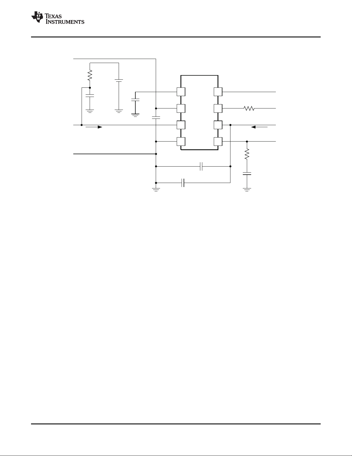
2
4
7
6
VSD
VDD
FB
GND
5GD
8LPM1 SS
3 PCS
C
SS
3.3 nF
C
VDD
100 nF
UDG-09221
TPS92010
C
BIAS
1 mF
R
GD
10 W
C
GD
1.0 nF
R
VSD
500 W
C
FBT
47 pF
LPM
V
VSD
V
DD
V
GD
[A]
C
PCST
560 pF
[A]
R
PCST
37.4 kW
+
V
FB
V
PCS
GND
I
PCS
I
VDD
TPS92010
www.ti.com
A. R
PCST
tests.
and C
SLUSA14 –DECEMBER 2009
OPEN LOOP TEST CIRCUIT
are not connected for maximum and minimum duty cycle tests, current sense tests and power limit
PCST
Copyright © 2009, Texas Instruments Incorporated Submit Documentation Feedback 5
Product Folder Link(s): TPS92010
Page 6
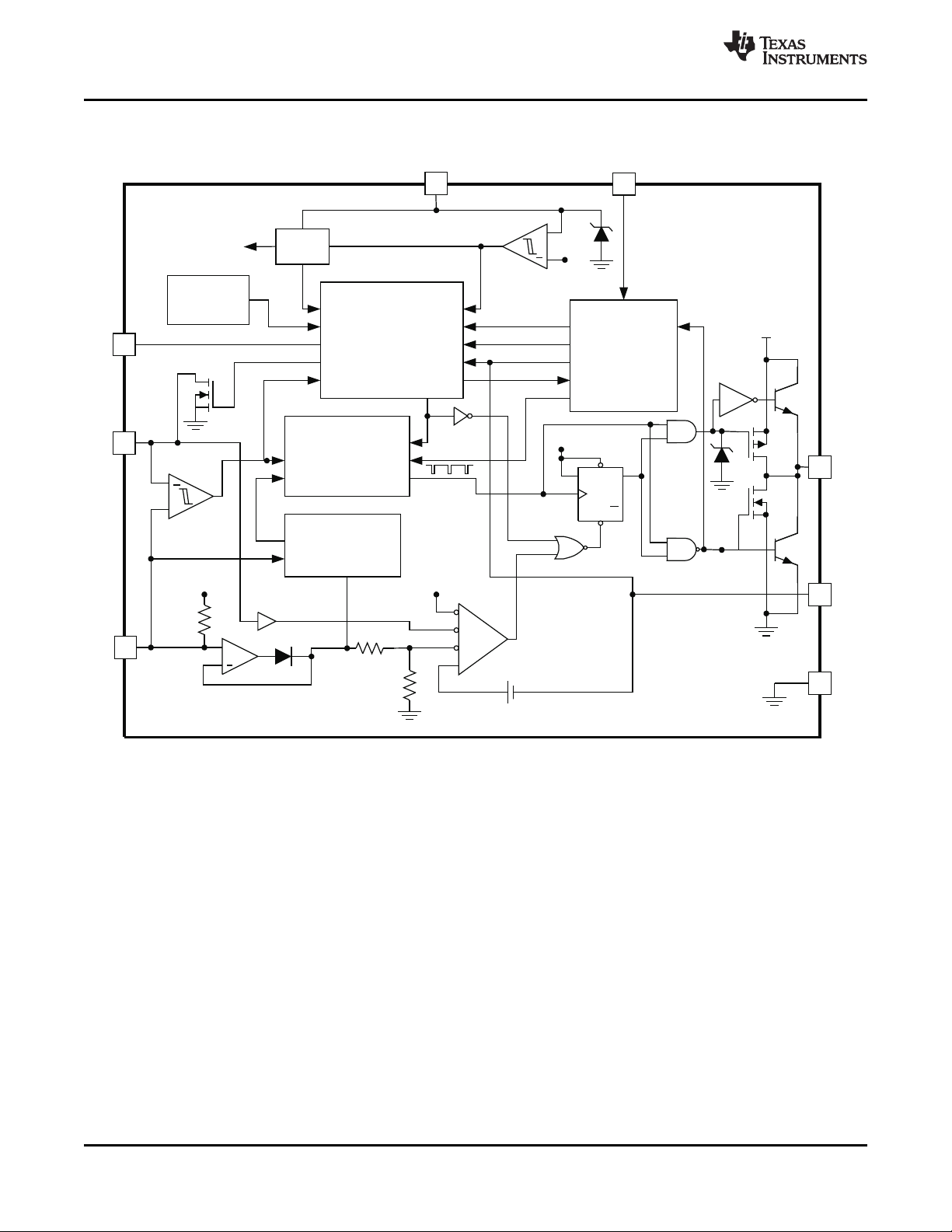
UDG-09222
2
1
6
5.0
VREF
SS
VDD
4
GND
5
GD
FB
1.5
R
8
3 PCS
UVLO
+
20
kW
7
VSD
On-Chip
Thermal
Shutdown
REF
26 V
R
LPM
13/8 V
+
400 mV
REF
+
Q
Q
SET
CLR
D
REF
GAIN = 1/2.5
+
Modulation
Comparison
TPS92010
Fault Logic
LINE_VSD
LOAD_VSD
REF_OK
RUN
UVLO
PCS
OVR_T
LPM
SS_DIS
Low Power Mode
FB_CLAMP
OSC_CL
FB
QR DETECT
LOAD_VSD
LINE_VSD
QR_DONE
___
GD
PCS
OSCILLATOR
QR_DONE
CLK
RUN
SS_OVR
OSC_CL
PL
1.2 V
SS_OVR LOW PWR LOW POWER
VDD
TPS92010
SLUSA14 –DECEMBER 2009
www.ti.com
BLOCK DIAGRAM
6 Submit Documentation Feedback Copyright © 2009, Texas Instruments Incorporated
Product Folder Link(s): TPS92010
Page 7
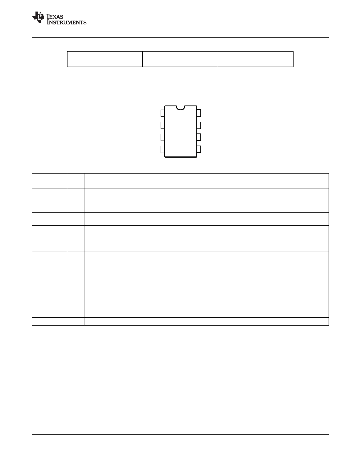
PCS
1
GND
2
3
4
SS
FB
VDD
8
GD
7
6
5
LPM
VSD
TPS92010
www.ti.com
SLUSA14 –DECEMBER 2009
ORDERING INFORMATION
T
A
–40°C to 105°C SOIC (D)
(1) SOIC (D) package is available taped and reeled by adding “R” to the above part numbers. Reeled
quantities for TPS92010DR is 2,500 devices per reel.
PACKAGES PART NUMBER
(1)
TPS92010D
DEVICE INFORMATION
TPS92010 (TOP VIEW)
PIN FUNCTIONS
PIN
NAME NO.
FB 2 I
GND 4 –
GD 5 O
LPM 8 O
PCS 3 I protection. The PCS voltage input originates across a current sense resistor and ground. Power limit is
SS 1 I placed as close as possible to the SS pin and GND, keeping trace length to a minimum. All faults discharge the
VDD 6 I as described in the GND pin description. Operating energy is usually delivered from auxiliary winding. To prevent
VSD 7 I The valley switching detect (VSD) pin senses line, load and resonant conditions using the primary bias winding.
I/O DESCRIPTION
Feedback input or control input from the output sensing network to the PWM comparator used to control the peak
current in the power MOSFET. An internal 20-kΩ resistor is between this pin and the internal 5-V regulated
voltage. The voltage of this pin controls the mode of operation in one of the three modes: quasi resonant (QR),
frequency foldback mode (FFM) and low power mode (LPM).
Ground for internal circuitry. Connect a ceramic 0.1-μF bypass capacitor between VDD and GND, with the
capacitor as close to these two pins as possible.
1-A sink (TrueDrive™ ) and 0.75-A source gate drive output. This output drives the power MOSFET and switches
between GND and the lower of VDD or the 13-V internal output clamp.
The low power mode pin is an ACTIVE HIGH open drain signal that indicates the device has entered low power
mode. LPM pin is high during UVLO, (VDD < startup threshold), and softstart, (SS < FB).
Peak current sense input, also programs power limit and is used to control modulation and activate overcurrent
programmed with an effective series resistance between this pin and the current sense resistor.
Soft-start programming pin. Program the soft-start rate with a capacitor to ground; the rate is determined by the
capacitance and the internal soft-start charge current. Placement of the soft-start capacitor is critical and should be
SS pin to GND through an internal MOSFET with an R
comparator reacts to the lowest of the SS voltage, the internal FB voltage and the peak current limit.
Provides power to the device. Use a ceramic 0.1-μF by-pass capacitor for high-frequency filtering of the VDD pin,
hiccup operation during start-up, a larger energy storage cap is also needed between VDD and GND.
of approximately 100 Ω. The internal modulator
DS(on)
Copyright © 2009, Texas Instruments Incorporated Submit Documentation Feedback 7
Product Folder Link(s): TPS92010
Page 8

START
VDD > 13V?
Soft Start
Monitor V
FB
VFB> 2.0V1.4V < VFB< 2.0VVFB< 1.4V
Fixed V/s
Freq. Foldback
(Light Load)
Quasi-Resonant
Mode or DCM
(Normal Load)
VFB< 0.5V
VDD < 8V?
REF < 4V?
VSD = Logic High?
OT = Logic High?
OC = Logic High
RUN = Logic High
LPM = Hi Z
Y
N
Y
Y
RUN = Logic Low
LPM = Hi Z
Fixed V-sec
40 kHz Burst
N
N
Fixed V/s
40kHz
Zero Pulses
LPM = Hi Z
(In Low Power
Mode)
VFB> 1.2V?VFB> 1.5V?
LPM = 0 V
(In Run-Mode)
LPM = 0V
(In Run-Mode)
LPM = 0V
(In Run-Mode)
N
N
YY
RUN = Logic Low
Continuous Fault
Monitor
UDG-09136
TPS92010
SLUSA14 –DECEMBER 2009
www.ti.com
APPLICATION INFORMATION
FUNCTIONAL DESCRIPTION
The TPS92010 is a multi-mode LED Lighting controller, as illustrated in Figure 1 and Figure 2. The mode of
operation depends upon input and dimming conditions. Under all modes of operation, the TPS92010 terminates
the GD = HI signal based on the switch current. Thus, the TPS92010 always operates in current mode control so
that the power MOSFET current is always limited.
8 Submit Documentation Feedback Copyright © 2009, Texas Instruments Incorporated
Figure 1. Control Flow Chart
Product Folder Link(s): TPS92010
Page 9

f
SW
Constant Volt-
seconds (ZCS)
Low Power
Mode
f
MAX
= Oscillator
Frequency
(130 kHz)
f
QR_MIN
: (internally
limited to 40 kHz.
QR Mode
(ZVS)
Switching
Frequency
V
FB
Feedback
Voltage
V
OUT
Power Supply
Output Voltage
SS Mode
(fixed fSW)
t
t
t
f
SS
(40 kHz)
f
LPM_MX
(40 kHz)
This mode applies bursts of 40
kHz soft-start pulses to the power
MOSFET gate. The average f
SW
is shown in this operating mode.
DCM
(maximum fS)
Hysteretic
transition into
Low Power
Mode.
IC Off
Softstart
Regular Operation Frequency Foldback
Low Power Mode
Peak MOSFET
Current
Load shown is slightly less
than overcurrent threshold
t
Fixed Frequency
V
LPM
LPM, pulled up to
VDD
t
Low Power Mode,
PFC bias OFF
P
OUT
Load Power
t
P
OUT
UDG-09137
TPS92010
www.ti.com
SLUSA14 –DECEMBER 2009
Figure 2. Operation Mode Switching Frequencies
Copyright © 2009, Texas Instruments Incorporated Submit Documentation Feedback 9
Product Folder Link(s): TPS92010
Page 10

VFBControl Range Limit
Internal Reference
fSW= 40 kHz
fSW= 130 kHz
0.5
0.7
1.4
2.0
4.0
5.0
0
Burst Hysteresis
Low Power
Mode
Burst-OFF
Burst-ON
Frequency Foldback Mode
QR Mode
or
DCM Mode
VFB(V)
TPS92010
SLUSA14 –DECEMBER 2009
www.ti.com
Under normal operating conditions, the FB pin commands the operating mode of the TPS92010 at the voltage
thresholds shown in Figure 3. Soft-start and fault responses are exceptions. During soft-start mode the
TPS92010 controls the converter at a fixed constant switching frequency of 40 kHz. The soft-start mode is
latched-OFF when VFBbecomes less than VSSfor the first time after UVLOON. The soft-start state cannot be
recovered until after passing UVLO
, and then, UVLOON.
OFF
At normal rated operating loads (from 100% to approximately 30% full rated power) the TPS92010 controls the
converter in quasi-resonant mode (QRM) or discontinuous conduction mode (DCM), where DCM operation is at
the clamped maximum switching frequency (130 kHz). For loads that are between approximately 30% and 10%
full rated power, the converter operates in frequency foldback mode (FFM), where the peak switch current is
constant and the output is regulated by modulating the switching frequency for a given and fixed VIN. Effectively,
operation in FFM results in the application of constant volt-seconds to the flyback transformer each switching
cycle. Voltage regulation in FFM is achieved by varying the switching frequency in the range from 130 kHz to 40
kHz. For extremely light loads (below approximately 10% full rated power), the converter is controlled using
bursts of 40-kHz pulses. Keep in mind that the aforementioned boundaries of steady-state operation are
approximate because they are subject to converter design parameters.
Refer to the typical applications block diagram for the electrical connections to implement the features.
Figure 3. Mode Control with FB Pin Voltage
10 Submit Documentation Feedback Copyright © 2009, Texas Instruments Incorporated
Product Folder Link(s): TPS92010
Page 11

UDG-09139
+
+
+
450 kW
450 kW
100 kW
100 kW
FB_CL
OSC_CL
FB
1.4 V
2.0 V
OSC_CL
QR_DONE
4.0V
0.1V
SS_OVR
REF
S Q
QR
CLK
130 kHz OSC
Clamp
Comparator
OSC Valley
Comparator
OSC Peak
Comparator
RUN
+
+
+
UDG-09138
TPS92010
www.ti.com
SLUSA14 –DECEMBER 2009
Details of the functional boxes in the Block Diagram are shown in Figure 4, Figure 5, Figure 6 and Figure 7
showing how the TPS92010 executes the command of the FB voltage to have the responses that are shown in
Figure 3, Figure 1 and Figure 2. The details of the functional boxes also show the various fault detections and
responses that are included in the TPS92010. During all modes of operation, this controller operates in current
mode control. This allows the TPS92010 to monitor the FB voltage to determine and respond to the varying load
levels.
Quasi-resonant mode and DCM occurs for feedback voltages VFBbetween 2.0 V and 4.0 V, respectively. In turn,
the PCS voltage is commanded to be between 0.4 V and 0.8 V. A cycle-by-cycle power limit imposes a fixed
0.8-V limit on the PCS voltage. An overcurrent shutdown threshold in the fault logic gives added protection
against high-current, slew-rate shorted winding faults, shown in Figure 7. The power limit feature in the QR
DETECT circuit of Figure 6 adds an offset to the PCS signal that is proportional to the line voltage. The power
limit feature is programmed with RPL, as shown in the typical application diagram.
Figure 4. Oscillator Details Figure 5. Mode Clamp Details
Copyright © 2009, Texas Instruments Incorporated Submit Documentation Feedback 11
Product Folder Link(s): TPS92010
Page 12

R
SU
C
IN
C
VDD
Auxiliary
Winding
+
+
+
+
7
Slope
+
0.1V
0.1V
–0.1V
REF(5V)
1kW
3.75V
0.45V
QR_DONE
(Oscillator)
LOAD_VSD
(FaultLogic)
LINE_VSD
(FaultLogic)
REF(5V)
3PCS
VSD
VDD
GD(FromDriver)
TPS92010
R
PL1
PCS
PowerLimit
Offset
I
LINE
LowPower
(fromFAULT logic)
01
+
QRDetect
I
LINE
I
LINE
2
C
OUT
R
PL2
N
S
N
P
N
B
R
VSD1
R
VSD2
R
PCS
UDG-09223
TPS92010
SLUSA14 –DECEMBER 2009
www.ti.com
Figure 6. QR Detect Details
12 Submit Documentation Feedback Copyright © 2009, Texas Instruments Incorporated
Product Folder Link(s): TPS92010
Page 13

S Q
QR
REF
D Q
Q
CLR
SET
Power-Up Reset
Thermal
Shutdown
+
+
1.25 V
0.6 V/0.7 V
+
SS/DIS
RUN
3 PCS
OVR_T
LINE_VSD
(QR Detect)
LOAD_VSD
(QR Detect)
UVLO
REF_OK
Low
Power
20 kW
REF
(5 V)
FB
7
FB
PCS
SS_OVR
0.6 V/1.5 V
LPM8
TPS92010
Low
Power
UDG-09224
TPS92010
www.ti.com
SLUSA14 –DECEMBER 2009
Figure 7. Fault Logic Details
Quasi-Resonant / DCM Control
Quasi-resonant (QR) and DCM operation occur for feedback voltages VFBbetween 2.0 V and 4.0 V. In turn, the
peak PCS voltage is commanded to be between 0.4 V and 0.8 V. During this control mode, the rising edge of GD
always occurs at the valley of the resonant ring after demagnetization. Resonant valley switching is an integral
part of QR operation. Resonant valley switching is also imposed if the system operates at the maximum
switching frequency clamp. In other words, the frequency varies in DCM operation in order to have the switching
event occur on the first resonant valley that occurs after a 7.7-μs (130-kHz) interval. Notice that the PCS pin has
an internal dependent current source, ½ I
function that is discussed in the Protection Features section.
Frequency Foldback Mode Control
Frequency foldback mode uses elements of the FAULT LOGIC, shown in Figure 7 and the mode clamp circuit,
shown in Figure 5. At the minimum operating frequency, the internal oscillator sawtooth waveform has a peak of
4.0 V and a valley of 0.1 V. When the FB voltage is between 2.0 V and 1.4 V, the FB_CL signal in Figure 5
commands the oscillator in a voltage controlled oscillator (VCO) mode by clamping the peak oscillator voltage.
The additional clamps in the OSCILLATOR restrict VCO operation between 40 kHz and 130 kHz. The FB_CL
voltage is reflected to the modulator comparator effectively clamping the reflected PCS command to 0.4 V.
. This current source is part of the cycle-by-cycle power limit
LINE
Copyright © 2009, Texas Instruments Incorporated Submit Documentation Feedback 13
Product Folder Link(s): TPS92010
Page 14

TPS92010
SLUSA14 –DECEMBER 2009
www.ti.com
Low Power Mode Control
Low power mode uses elements of the FAULT LOGIC, shown in Figure 7 and the mode clamps circuit, shown in
Figure 5. The OSC_CL signal clamps the Low Power-mode operating frequency at 40 kHz. Thus, when the FB
voltage is between 1.4 V and 0.5 V, the controller is commanding an excess of energy to be transferred to the
load which in turn, drives the error higher and FB lower. When FB reaches 0.5 V, GD pulses are terminated and
do not resume until FB reaches 0.7 V. In this mode, the converter operates in hysteretic control with the GD
pulse terminated at a fixed PCS voltage level of 0.4 V. The power limit offset is turned OFF during Low Power
mode and it returns to ON when FB is above 1.4 V, as depicted in Figure 7. H mode reduces the average
switching frequency in order to minimize switching losses and increase the efficiency at light load conditions.
Fault Logic
Advanced logic control coordinates the fault detections to provide proper power supply recovery. This provides
the conditioning for the thermal protection. Line overvoltage protection and load overvoltage protection are
implemented in this block. It prevents operation when the internal reference is below 4.5 V. If a fault is detected
in the thermal shutdown, line overvoltage protection, load overvoltage protection, or REF, the TPS92010
undergoes a shutdown/retry cycle.
Refer to the fault logic diagram in Figure 7 and the QR detect diagram in Figure 6 to program line overvoltage
protection and load overvoltage protection. To program the load overvoltage protection, select the R
VSD1
– R
VSD2
divider ratio to be 3.75 V at the desired output shut-down voltage. To program line overvoltage protection, select
the impedance of the R
VSD1
– R
combination to draw 450 μA when the V
VSD2
is 0.45 V during the ON-time of
VSD
the power MOSFET at the highest allowable input voltage.
Oscillator
The oscillator, shown in Figure 4, is internally set and trimmed so it is clamped by the circuit in Figure 4 to a
nominal 130-kHz maximum operating frequency. It also has a minimum frequency clamp of 40 kHz. If the FB
voltage tries to drive operation to less than 40 kHz, the converter operates in low power mode.
Low Power
The LPM pin is an open drain output, as shown in Figure 7. The LPM output goes into the OFF-state when FB
falls below 0.5 V and it returns to the ON-state (low impedance to GND) when FB rises above 1.4 V.
OPERATING MODE PROGRAMMING
Boundaries of the operating modes are programmed by the flyback transformer and the four components RPL,
R
PCS
, R
VSD1
and R
; shown in Figure 1.
VSD2
The transformer characteristics that predominantly affect the modes are the magnetizing inductance of the
primary and the magnitude of the output voltage, reflected to the primary. To a lesser degree (yet significant), the
boundaries are affected by the MOSFET output capacitance and transformer leakage inductance. The design
procedure here is to select a magnetizing inductance and a reflected output voltage that operates at the
DCM/CCM boundary at maximum load and maximum line. The actual inductance should be noticeably smaller to
account for the ring between the magnetizing inductance and the total stray capacitance measured at the drain
of the power MOSFET. This programs the QR/DCM boundary of operation. All other mode boundaries are preset
with the thresholds in the oscillator and green-mode blocks.
PROTECTION FEATURES
The TPS92010 has many protection features. Refer to Figures 1, 4, 8, 9 and 10 for detailed block descriptions
that show how the features are integrated into the normal control functions.
Overtemperature
Overtemperature lockout typically occurs when the substrate temperature reaches 140ºC. Retry is allowed if the
substrate temperature reduces by the hysteresis value. Upon an overtemperature fault, CSSon softstart is
discharged and LPM is forced to a high impedance.
Cycle-by-Cycle Power Limit
The cycle terminates when the PCS voltage plus the power limit offset exceeds 1.2 V.
14 Submit Documentation Feedback Copyright © 2009, Texas Instruments Incorporated
Product Folder Link(s): TPS92010
Page 15

TPS92010
www.ti.com
SLUSA14 –DECEMBER 2009
In order to have power limited over the full line voltage range of the QR Flyback converter, the PCS pin voltage
must have a component that is proportional to the primary current plus a component that is proportional to the
line voltage due to predictable switching frequency variations due to line voltage. At power limit, the PCS pin
voltage plus the internal PCS offset is compared against a constant 1.2-V reference in the PWM comparator.
Thus during cycle-by-cycle power limit, the peak PCS voltage is typically 0.8 V.
The current that is sourced from the VSD pin (I
) is reflected to a dependent current source of ½ I
LINE
LINE
, that is
connected to the PCS pin. The power limit function can be programmed by a resistor, RPL, that is between the
PCS pin and the current sense resistor. The current, I
ratio NB/NPand resistor R
. Current I
VSD1
is programmed to set the line over voltage protection. Resistor R
LINE
, is proportional to line voltage by the transformer turns
LINE
PL
results in the addition of a voltage to the current sense signal that is proportional to the line voltage. The proper
amount of additional voltage has the effect of limiting the power on a cycle-by-cycle basis. Note that R
R
VSD1
and R
must be adjusted as a set due to the functional interactions.
VSD2
PCS
, RPL,
Current Limit
When the primary current exceeds maximum current level which is indicated by a voltage of 1.25 V at the PCS
pin, the device initiates a shutdown. Retry occurs after a UVLO
/UVLOONcycle.
OFF
Overvoltage Protection Function
Input line overvoltage and LED open string protection is programmed with the transformer turn ratios, R
R
. The VSD pin has a 0-V voltage source that can only source current; VSD cannot sink current.
VSD2
VSD1
and
Open String LED protection occurs when the VSD pin is clamped at 0 V. When the bias winding is negative,
during GD = HI or portions of the resonant ring, the 0-V voltage source clamps VSD to 0 V and the current that is
sourced from the VSD pin is mirrored to the Line_VSD comparator and the QR detection circuit. The Line_VSD
comparator initiates a shutdown-retry sequence if VSD sources any more than 450 μA.
Open String LED protection occurs when the VSD pin voltage is positive. When the bias winding is positive,
during demagnetization or portions of the resonant ring, the VSD pin voltage is positive. If the VSD voltage is
greater than 3.75 V, the device initiates a shutdown. Retry occurs after a UVLO
/UVLOONcycle.
OFF
Undervoltage Lockout
Protection is provided to guard against operation during unfavorable bias conditions. Undervoltage lockout
(UVLO) always monitors VDD to prevent operation below the UVLO threshold.
Copyright © 2009, Texas Instruments Incorporated Submit Documentation Feedback 15
Product Folder Link(s): TPS92010
Page 16

–40
22
20
–15
26
24
30
28
10 35 60 85 110 135
TJ– Junction Temperature – °C
V
DD
– Clamp Voltage – V
–40 –15 10 35 60 85 110 135
TJ– Junction Temperature – °C
124
120
132
128
140
136
f
SW(max)
– Maximum Switching Frequency – kHz
134
130
138
126
122
–40 –15 10 35 60 85 110 135
TJ– Junction Temperature – °C
770
750
810
790
850
830
V
PL
– Power Limit Threshold Voltage – mV
820
800
840
780
760
–40
–475
–500
–15
–450
–375
–400
10 35 60 85 110 135
TJ– Junction Temperature – °C
I
VSD
– Overcoltage Protection Current – mA
–425
TPS92010
SLUSA14 –DECEMBER 2009
JUNCTION TEMPERATURE JUNCTION TEMPERATURE
www.ti.com
TYPICAL CHARACTERISTICS
CLAMP VOLTAGE SWITCHING FREQUENCY
vs vs
Figure 8. Figure 9.
PL THRESHOLD OVERVOLTAGE PROTECTION THRESHOLD
vs vs
TEMPERATURE TEMPERATURE
16 Submit Documentation Feedback Copyright © 2009, Texas Instruments Incorporated
Figure 10. Figure 11.
Product Folder Link(s): TPS92010
Page 17

PACKAGE OPTION ADDENDUM
www.ti.com 5-Feb-2010
PACKAGING INFORMATION
Orderable Device Status
(1)
Package
Type
Package
Drawing
Pins Package
Qty
Eco Plan
TPS92010D ACTIVE SOIC D 8 75 Green (RoHS &
(2)
Lead/Ball Finish MSL Peak Temp
CU NIPDAU Level-1-260C-UNLIM
(3)
no Sb/Br)
TPS92010DR ACTIVE SOIC D 8 2500 Green (RoHS &
CU NIPDAU Level-1-260C-UNLIM
no Sb/Br)
(1)
The marketing status values are defined as follows:
ACTIVE: Product device recommended for new designs.
LIFEBUY: TI has announced that the device will be discontinued, and a lifetime-buy period is in effect.
NRND: Not recommended for new designs. Device is in production to support existing customers, but TI does not recommend using this part in
a new design.
PREVIEW: Device has been announced but is not in production. Samples may or may not be available.
OBSOLETE: TI has discontinued the production of the device.
(2)
Eco Plan - The planned eco-friendly classification: Pb-Free (RoHS), Pb-Free (RoHS Exempt), or Green (RoHS & no Sb/Br) - please check
http://www.ti.com/productcontent for the latest availability information and additional product content details.
TBD: The Pb-Free/Green conversion plan has not been defined.
Pb-Free (RoHS): TI's terms "Lead-Free" or "Pb-Free" mean semiconductor products that are compatible with the current RoHS requirements
for all 6 substances, including the requirement that lead not exceed 0.1% by weight in homogeneous materials. Where designed to be soldered
at high temperatures, TI Pb-Free products are suitable for use in specified lead-free processes.
Pb-Free (RoHS Exempt): This component has a RoHS exemption for either 1) lead-based flip-chip solder bumps used between the die and
package, or 2) lead-based die adhesive used between the die and leadframe. The component is otherwise considered Pb-Free (RoHS
compatible) as defined above.
Green (RoHS & no Sb/Br): TI defines "Green" to mean Pb-Free (RoHS compatible), and free of Bromine (Br) and Antimony (Sb) based flame
retardants (Br or Sb do not exceed 0.1% by weight in homogeneous material)
(3)
MSL, Peak Temp. -- The Moisture Sensitivity Level rating according to the JEDEC industry standard classifications, and peak solder
temperature.
Important Information and Disclaimer:The information provided on this page represents TI's knowledge and belief as of the date that it is
provided. TI bases its knowledge and belief on information provided by third parties, and makes no representation or warranty as to the
accuracy of such information. Efforts are underway to better integrate information from third parties. TI has taken and continues to take
reasonable steps to provide representative and accurate information but may not have conducted destructive testing or chemical analysis on
incoming materials and chemicals. TI and TI suppliers consider certain information to be proprietary, and thus CAS numbers and other limited
information may not be available for release.
In no event shall TI's liability arising out of such information exceed the total purchase price of the TI part(s) at issue in this document sold by TI
to Customer on an annual basis.
Addendum-Page 1
Page 18

PACKAGE MATERIALS INFORMATION
www.ti.com 20-Jul-2010
TAPE AND REEL INFORMATION
*All dimensions are nominal
Device Package
TPS92010DR SOIC D 8 2500 330.0 12.4 6.4 5.2 2.1 8.0 12.0 Q1
Type
Package
Drawing
Pins SPQ Reel
Diameter
(mm)
Reel
Width
W1 (mm)
A0
(mm)B0(mm)K0(mm)P1(mm)W(mm)
Pin1
Quadrant
Pack Materials-Page 1
Page 19

PACKAGE MATERIALS INFORMATION
www.ti.com 20-Jul-2010
*All dimensions are nominal
Device Package Type Package Drawing Pins SPQ Length (mm) Width (mm) Height (mm)
TPS92010DR SOIC D 8 2500 340.5 338.1 20.6
Pack Materials-Page 2
Page 20

Page 21

IMPORTANT NOTICE
Texas Instruments Incorporated and its subsidiaries (TI) reserve the right to make corrections, modifications, enhancements, improvements,
and other changes to its products and services at any time and to discontinue any product or service without notice. Customers should
obtain the latest relevant information before placing orders and should verify that such information is current and complete. All products are
sold subject to TI’s terms and conditions of sale supplied at the time of order acknowledgment.
TI warrants performance of its hardware products to the specifications applicable at the time of sale in accordance with TI’s standard
warranty. Testing and other quality control techniques are used to the extent TI deems necessary to support this warranty. Except where
mandated by government requirements, testing of all parameters of each product is not necessarily performed.
TI assumes no liability for applications assistance or customer product design. Customers are responsible for their products and
applications using TI components. To minimize the risks associated with customer products and applications, customers should provide
adequate design and operating safeguards.
TI does not warrant or represent that any license, either express or implied, is granted under any TI patent right, copyright, mask work right,
or other TI intellectual property right relating to any combination, machine, or process in which TI products or services are used. Information
published by TI regarding third-party products or services does not constitute a license from TI to use such products or services or a
warranty or endorsement thereof. Use of such information may require a license from a third party under the patents or other intellectual
property of the third party, or a license from TI under the patents or other intellectual property of TI.
Reproduction of TI information in TI data books or data sheets is permissible only if reproduction is without alteration and is accompanied
by all associated warranties, conditions, limitations, and notices. Reproduction of this information with alteration is an unfair and deceptive
business practice. TI is not responsible or liable for such altered documentation. Information of third parties may be subject to additional
restrictions.
Resale of TI products or services with statements different from or beyond the parameters stated by TI for that product or service voids all
express and any implied warranties for the associated TI product or service and is an unfair and deceptive business practice. TI is not
responsible or liable for any such statements.
TI products are not authorized for use in safety-critical applications (such as life support) where a failure of the TI product would reasonably
be expected to cause severe personal injury or death, unless officers of the parties have executed an agreement specifically governing
such use. Buyers represent that they have all necessary expertise in the safety and regulatory ramifications of their applications, and
acknowledge and agree that they are solely responsible for all legal, regulatory and safety-related requirements concerning their products
and any use of TI products in such safety-critical applications, notwithstanding any applications-related information or support that may be
provided by TI. Further, Buyers must fully indemnify TI and its representatives against any damages arising out of the use of TI products in
such safety-critical applications.
TI products are neither designed nor intended for use in military/aerospace applications or environments unless the TI products are
specifically designated by TI as military-grade or "enhanced plastic." Only products designated by TI as military-grade meet military
specifications. Buyers acknowledge and agree that any such use of TI products which TI has not designated as military-grade is solely at
the Buyer's risk, and that they are solely responsible for compliance with all legal and regulatory requirements in connection with such use.
TI products are neither designed nor intended for use in automotive applications or environments unless the specific TI products are
designated by TI as compliant with ISO/TS 16949 requirements. Buyers acknowledge and agree that, if they use any non-designated
products in automotive applications, TI will not be responsible for any failure to meet such requirements.
Following are URLs where you can obtain information on other Texas Instruments products and application solutions:
Products Applications
Amplifiers amplifier.ti.com Audio www.ti.com/audio
Data Converters dataconverter.ti.com Automotive www.ti.com/automotive
DLP® Products www.dlp.com Communications and www.ti.com/communications
DSP dsp.ti.com Computers and www.ti.com/computers
Clocks and Timers www.ti.com/clocks Consumer Electronics www.ti.com/consumer-apps
Interface interface.ti.com Energy www.ti.com/energy
Logic logic.ti.com Industrial www.ti.com/industrial
Power Mgmt power.ti.com Medical www.ti.com/medical
Microcontrollers microcontroller.ti.com Security www.ti.com/security
RFID www.ti-rfid.com Space, Avionics & www.ti.com/space-avionics-defense
RF/IF and ZigBee® Solutions www.ti.com/lprf Video and Imaging www.ti.com/video
Mailing Address: Texas Instruments, Post Office Box 655303, Dallas, Texas 75265
Copyright © 2010, Texas Instruments Incorporated
Telecom
Peripherals
Defense
Wireless www.ti.com/wireless-apps
 Loading...