T
TPS9125
5 V/3 V SIM SUPPLY AND LEVEL SHIFTERS
SLVS244A – SEPTEMBER 1999 – REVISED NOVEMBER 1999
D
Integrated SIM Supply and Level Shifters
D
Selectable 5-V or 3-V SIM Supply Voltage
D
3-V to 5-V Level Shifters, Bidirectional for
SIM Data Line
D
10 kV ESD Protection (HBM) on SIMDATA,
SIMRST, and SIMCLK Terminal
D
14 Terminal TSSOP
D
Minimum Supply Voltage 2.7 V
D
Integrated PullUp Resistor for DATA and
V
DD
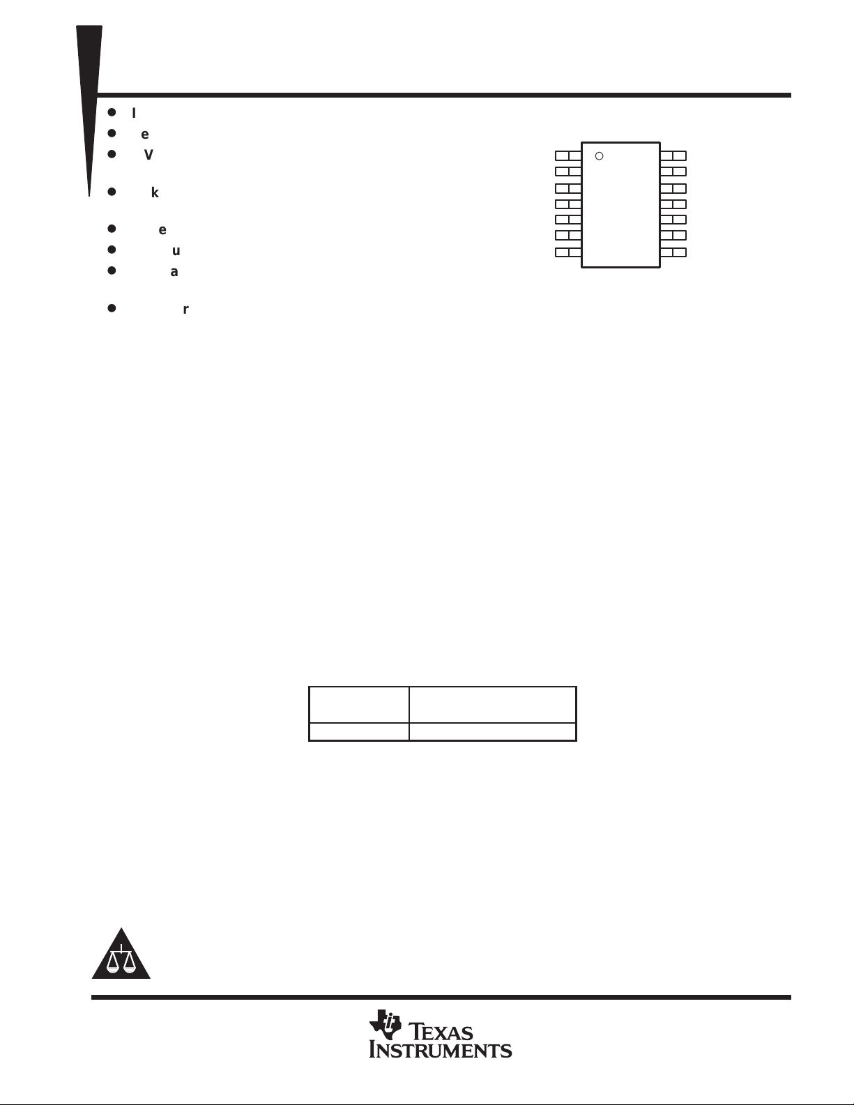
RESET
MODE
SIMPWR
DATA
CLK
RST
PW PACKAGE
(TOP VIEW)
1
2
3
4
5
6
7
14
13
12
11
10
9
8
SIMVCC
VCAP1
VCAP2
SIMDATA
GND
SIMCLK
SIMRST
SIMDATA
D
Thin Shrink, Small Outline, Left-Hand Tape
and Reel Package
description
The TPS9125 SIM supply and level shifter integrates a programmable 3-V or 5-V SIM supply , conformable to
the (GSM) test specification 11.10, together with either a 3-V or 5-V level shifter, conformable to the GSM
specification 11.11 and 11.12.
A charge pump, utilizing two external capacitors, is configured as voltage doubler to generate a 5-V supply rail
from VDD. Dependent on the SIM card used, a control signal coming from the SIM card controller is applied on
the MODE terminal to switch between a 3-V or 5-V supply on the SIMVCC output terminal.
A 3-V/5-V bidirectional level shifter translates the 3-V compatible logic signal on DATA terminal into a 5-V
compatible logic signal SIMDATA terminal, and vice versa. RST and CLK are unidirectional level shifters,
providing a 5-V SIMRST and SIMCLK signal from the microcontroller to the SIM card.
The SIM supply is operating provided SIMPWR = 1 and VDD is sufficient (> 2.7 V). Under this condition, SIMVCC
voltage is generated by the SIM supply charge pump.
A RESET terminal is provided for security reasons to switch off the SIM supply and interface if the SIM card is
disconnected or removed by accident.
The TSP9125 is packaged in TI’s thin shrink small-outline package (PW).
AVAILABLE OPTIONS
A
–30°C to 85°C TSP9125PWR
†
Suffix R stands for left-handed tape and reel.
Please be aware that an important notice concerning availability, standard warranty, and use in critical applications of
Texas Instruments semiconductor products and disclaimers thereto appears at the end of this data sheet.
PACKAGE
(PW)
†
TI is a trademark of Texas Instruments Incorporated.
PRODUCTION DATA information is current as of publication date.
Products conform to specifications per the terms of Texas Instruments
standard warranty. Production processing does not necessarily include
testing of all parameters.
POST OFFICE BOX 655303 • DALLAS, TEXAS 75265
Copyright 1999, Texas Instruments Incorporated
1
TPS9125
I/O
DESCRIPTION
5 V/3 V SIM SUPPLY AND LEVEL SHIFTERS
SLVS244A – SEPTEMBER 1999 – REVISED NOVEMBER 1999
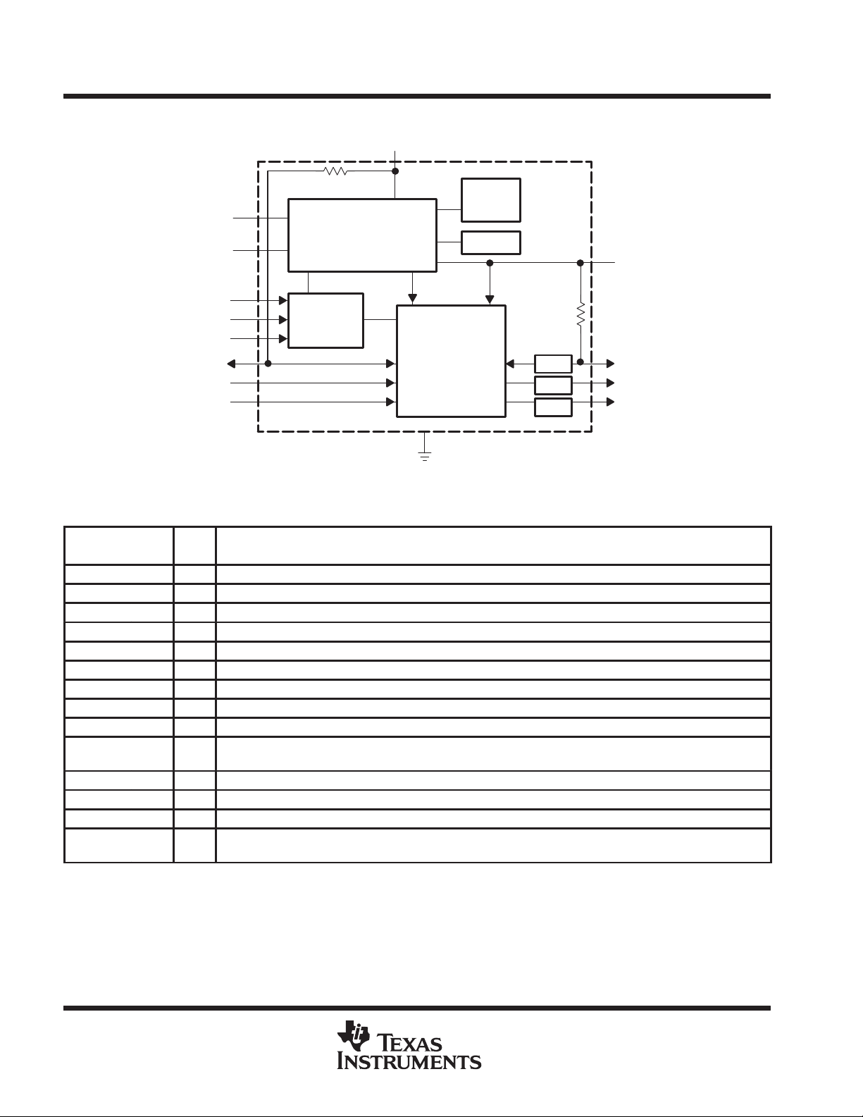
functional block diagram
V
DD
VCAP1
VCAP2
SIMPWR
MODE
RESET
DATA
CLK
RST
20 kΩ
Voltage
Generator
(Charge Pump)
Control
Control
Block
Block
Shifter
VDD or
SIMVCC
Level
GND
OSC
800 kHz
VREF
10 kΩ
ESD
ESD
ESD
SIMVCC
SIMDATA
SIMCLK
SIMRST
Terminal Functions
TERMINAL
NAME NO.
CLK 6 DI 3-V SIM clock signal. This terminal is connected to the SIM interface and works with 3-V logic level.
DATA 5 DI/O 3-V bidirectional data line. This terminal is connected to the SIM interface and works with 3-V logic level.
GND 10 Ground
MODE 3 DI Programs the SIM supply voltage to SIMVCC = 5 V (MODE = 0) or SIMVCC = 3 V (MODE = 1).
RESET 2 DI Reset for the TSP9125 SIM supply and interface in case the SIM is removed under operation.
RST 7 DI 3-V SIM reset signal. This terminal is connected to the SIM interface and works with 3-V logic level.
SIMCLK 9 DO 3-V/5-V SIM clock signal. This terminal is connected to the SIM reader contacts.
SIMRST 8 DO 3-V/5-V SIM reset signal. This terminal is connected to the SIM reader contacts.
SIMDATA 11 DI/O 3-V/5-V bidirectional data line. This terminal is connected to the SIM reader contacts.
SIMVCC 14
SIMPWR 4 DI SIM supply enable terminal. SIMPWR = 0 leaves SIMVCC open, SIMPWR = 1 enables SIM supply.
VCAP1 13 Charge pump capacitor. Connect 220 nF ±20% capacitor between VCAP1 and VCAP2.
VCAP2 12 Charge pump capacitor. Connect 220 nF ±20% capacitor between VCAP1 and VCAP2.
V
DD
1
SIM supply voltage. Can be switched between 5 V ±10% and 3 V ±10%. This terminal is connected to the SIM
reader contacts. Connect a 1 µF ±20% capacitor between SIMVCC and GND.
Supply voltage input. Connect a power bypass capacitor of 1 µF between VDD and GND. Connect capacitor
physically close to the VDD terminal.
2
POST OFFICE BOX 655303 • DALLAS, TEXAS 75265
5 V/3 V SIM SUPPLY AND LEVEL SHIFTERS
SLVS244A – SEPTEMBER 1999 – REVISED NOVEMBER 1999
detailed description
voltage generator (charge pump)
The voltage generator can be programmed in two modes:
1. SIMPWR = 0: SIMVCC is left open, voltage generator disabled.
2. SIMPWR = 1: Depending on the signal on control terminal MODE, SIMVCC is either programmed to:
a. MODE = 0: 5 V ±10% (this is the default condition under which the system powers up),
or
b. MODE = 1: SIMV
The setting of the SIMVCC voltage (MODE = 0 or 1) can only be changed when SIMPWR is low. Therefore, as
specified in GSM11.12, supply voltage switching is performed by deactivating the SIM and activating it at the
new supply voltage.
In 5-V mode, a regulated charge pump is used to step-up the 3-V supply rail (min 2.7 V) to the 5-V supply rail.
The voltage generator uses two external capacitors, one pump capacitor connected between VCAP1 and
VCAP2 and one output buffer capacitor connected between SIMVCC and GND. It operates at a nominal
frequency of 800 kHz, and also supplies the integrated level shifters to allow for 5-V compatible logic signals
on SIMRST, SIMCLK, and SIMDATA.
is equal to the supply voltage VDD minus a voltage drop of 50 mV maximum.
CC
TPS9125
In 3-V mode, the supply voltage VDD is connected via an integrated PMOS switch to the SIMVCC output. The
charge pump, oscillator, and voltage reference are disabled in the 3-V mode to reduce power consumption. The
supply voltage of the integrated level shifters is V
minus a voltage drop of 50 mV maximum.
DD
control block
The control block uses the three control signals SIMPWR, MODE, and RESET to set the TSP9125 operation
modes.
When SIMPWR is set low, the TSP9125 goes to power-down mode. To comply with the ISO/IEC 7816-3
specification for deactivation of the SIM contacts, the input terminals RST, DA TA, and CLK must be low before
the SIMPWR terminal is allowed to be taken low. When SIMPWR is low, the SIMRST, SIMDA TA, and SIMCLK
terminals are kept low and SIMVCC is left open.
The RESET input is used to disable the TSP9125 in case the SIM card is removed from the reader under
operation. The input is therefore typically connected to a mechanical or other device used to detect the removal
of the SIM card. When RESET is taken low, the SIMDAT A, SIMCLK, and SIMRST terminals are taken low and
SIMVCC is left open, until RESET is taken high again.
Table 1. Control Block Function Table
RESET MODE SIMPWR OPERATING MODE
0 X X SIM supply disabled; SIMVCC open; SIMRST and SIMCLK and SIMDATA low
1 0 0 TSP9125 in power-down mode. SIM supply disabled; SIMVCC open; SIMRST, SIMCLK, and SIMDA T A low;
1 1 0 TSP9125 in power-down mode. SIM supply disabled; SIMVCC open; SIMRST, SIMCLK, and SIMDA T A low;
1 X 1 TSP9125 in normal operation mode; SIM supply enabled, SIMVCC = 5 V or 3 V depending on how it was
SIMVCC programmed to 5-V mode.
SIMVCC programmed to 3-V mode.
programmed.
POST OFFICE BOX 655303 • DALLAS, TEXAS 75265
3
TPS9125
5 V/3 V SIM SUPPLY AND LEVEL SHIFTERS
SLVS244A – SEPTEMBER 1999 – REVISED NOVEMBER 1999
detailed description (continued)
level shifters
The level shifters on TSP9125, when operating in the 5-V mode, convert a 3-V compatible logic signal from a
digital control chip (SIM Controller) into a 5-V compatible logic signal for the SIM Card.
Operating in the 3-V mode, the level shifters are disabled and only pass the signal through.
The level shifters for reset and clock signal are unidirectional (RST to SIMRST, CLK to SIMCLK). The level
shifter for the data signal is bidirectional, enabling signal exchange in both directions (DA TA to SIMDATA and
SIMDATA to DATA).
During power up and power down of the TSP9125, the voltage level on the SIMRST, SIMCLK, and SIMDAT A
terminals is kept below 0.4 V for currents less than 1 mA flowing into the TSP9125, provided VDD is applied.
pullup resistors
The DA TA and SIMDATA I/O pullup resistors are integrated in the device. The DATA resistor is 20 kΩ and the
SIMDATA resistor is 10 kΩ.
oscillator
An integrated RC oscillator provides the charge pump with a nominal clock frequency of 800 kHz.
voltage reference
An integrated bandgap reference provides a reference voltage of 1.192 V to the charge pump to control and
regulate the output voltage.
ESD protection
In a cellular telephone (GSM phone) the SIMRST, SIMCLK, and SIMDA TA terminals are connected directly to
the contacts of the SIM reader. This means they are accessible from the outside and therefore require increased
ESD protection. The terminals withstand 10 kV ESD when tested according to human body model (HBM),
100 pF through 1500 Ω.
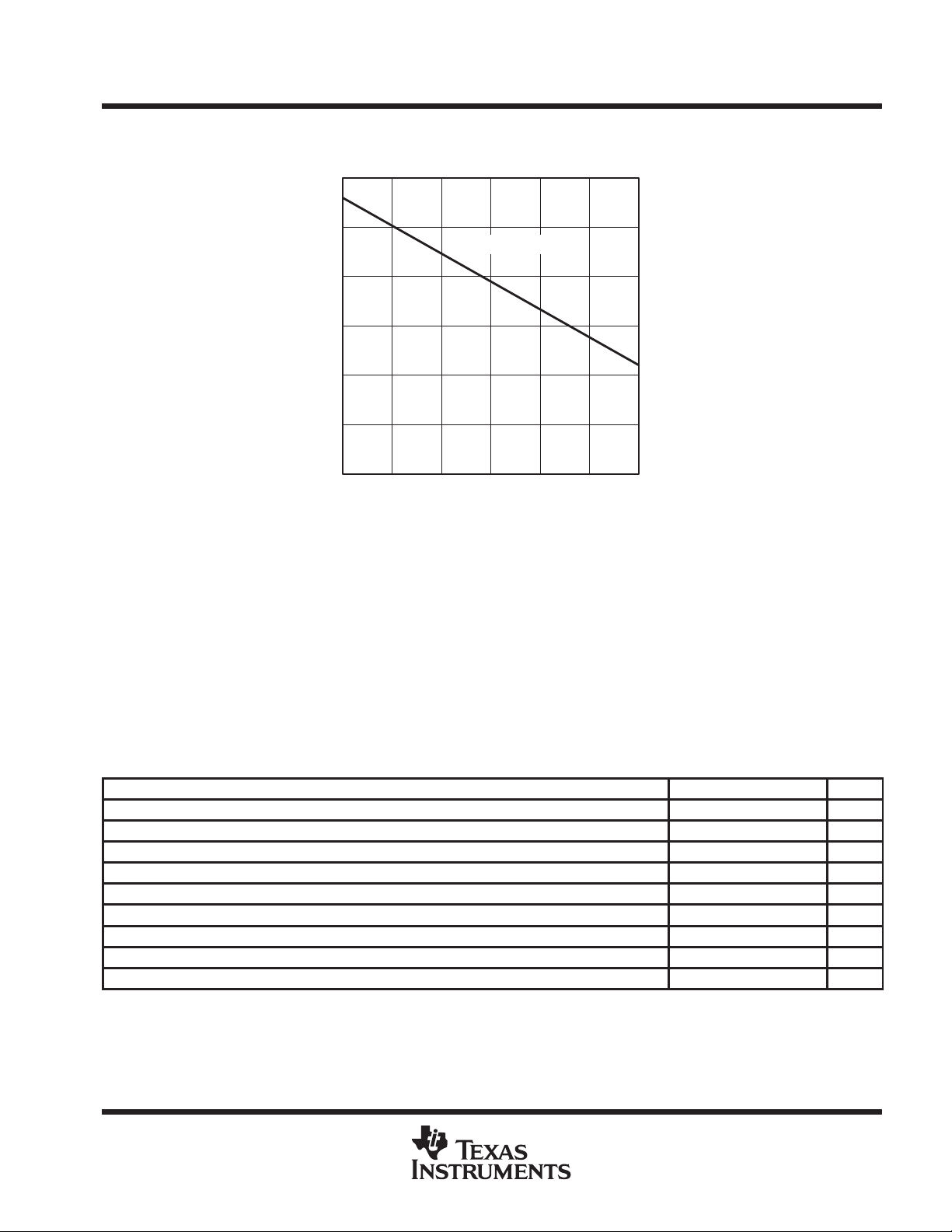
DISSIPATION RATING TABLE
PACKAGED
PW 556 mW 5.56 mW/°C 306 mW
TA < 25°C
POWER RATING
OPERATING FACTOR
ABOVE TA = 25°C
TA = 70°C
POWER RATING
4
POST OFFICE BOX 655303 • DALLAS, TEXAS 75265
TPS9125
5 V/3 V SIM SUPPLY AND LEVEL SHIFTERS
SLVS244A – SEPTEMBER 1999 – REVISED NOVEMBER 1999
DISSIPATION DERATING CURVE
vs
FREE-AIR TEMPERATURE
6
5
RthJA – 180°C/W
4
3
2
Power Dissipation – mW
1
0
25 35 45 55
TA – Free-Air Temperature – °C
absolute maximum ratings over operating free-air temperature (unless otherwise noted)
65 75 85
†
Supply voltage range, VDD –0.3V to 4 V. . . . . . . . . . . . . . . . . . . . . . . . . . . . . . . . . . . . . . . . . . . . . . . . . . . . . . . . . . .
Input voltage range, all other terminals –0.3V to V
DD
+ 0.3V. . . . . . . . . . . . . . . . . . . . . . . . . . . . . . . . . . . . . . . . .
Peak output current, SIMVCC 20 mA. . . . . . . . . . . . . . . . . . . . . . . . . . . . . . . . . . . . . . . . . . . . . . . . . . . . . . . . . . . . . .
Free-air temperature range –40°C to 85°C. . . . . . . . . . . . . . . . . . . . . . . . . . . . . . . . . . . . . . . . . . . . . . . . . . . . . . . . .
Storage temperature range –60°C to 125°C. . . . . . . . . . . . . . . . . . . . . . . . . . . . . . . . . . . . . . . . . . . . . . . . . . . . . . . .
Continuous total power dissipation 0.1 W. . . . . . . . . . . . . . . . . . . . . . . . . . . . . . . . . . . . . . . . . . . . . . . . . . . . . . . . . .
†
Stresses beyond those listed under “absolute maximum ratings” may cause permanent damage to the device. These are stress ratings only, and
functional operation of the device at these or any other conditions beyond those indicated under “recommended operating conditions” is not
implied. Exposure to absolute-maximum-rated conditions for extended periods may affect device reliability.
recommended operating conditions
MIN NOM MAX UNIT
Supply voltage, V
Charge pump capacitor between VCAP1 and VCAP2 220 nF
Charge pump output capacitor on SIMVCC 1 µF
Input capacitor on VDD 0.1 1 µF
Operating free-air temperature range –30 85 °C
Operating virtual junction temperature range –30 125 °C
ESD susceptibility kV
SIMRST, SIMCLK, SIMDATA (human body model, 100 pF through 1500 Ω) 10 (TBC) kV
All other terminals (human body model, 100 pF through 1500 Ω) 2
DD
2.7 3 3.3 V
POST OFFICE BOX 655303 • DALLAS, TEXAS 75265
5
TPS9125
Clock frequency CLK/SIMCLK
MH
5 V/3 V SIM SUPPLY AND LEVEL SHIFTERS
SLVS244A – SEPTEMBER 1999 – REVISED NOVEMBER 1999
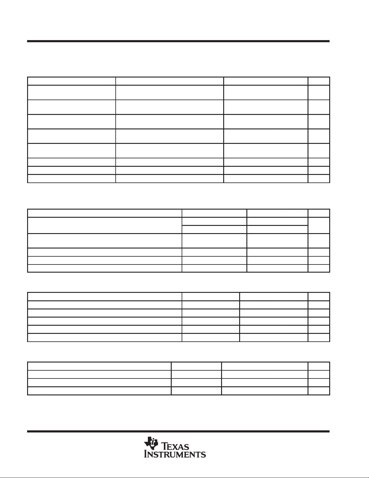
electrical characteristics over recommended operating junction temperature range, VDD = 3 V,
C
VCAP1/2
= 220 nF ±20%; C
SIMVCC
voltage generator charge pump (SIMVCC)
PARAMETER TEST CONDITIONS MIN TYP MAX UNIT
Output voltage at SIMVCC, 5-V mode
Output voltage at SIMVCC, 3-V mode
Output current at SIMVCC, 5-V mode
(see Note 1)
Output current at SIMVCC, 3-V mode
(see Note 1)
Switching frequency (internal oscillator
frequency)
Output ripple 5-V mode, I
Startup time Standby to 5-V mode 1 ms
Power efficiency I
NOTE 1: The SIM supply circuit is designed according to the GSM specification 11.11 and 1 1.12 and complies to the requirements of GSM test
specification 11.10. For more information, please see application section.
2.7 V < VDD < 3.3 V,
f
2.7 V < VDD < 3.3 V,
MODE = 1
2.7 V < VDD < 3.3 V 10 mA
2.7 V < VDD < 3.3 V 6 MA
= 1 µF ±20%; SIMPWR = 1 (unless otherwise noted)
SIMCLK
SIMVCC
I
= 0 MHz,
= 10 mA 82.5%
SIMVCC
MODE = 0 (default value)
I
SIMVCC
out
= 10 mA,
= 6 mA,
= 10 mA 100 mV
4.5 5.5 V
VDD–50 mV VDD–50 mV V
440 800 1 160 kHz
level shifters (see Note 2)
PARAMETER TEST CONDITIONS MIN TYP MAX UNIT
5-V mode 1 5
3-V mode 1 4
Clock duty cycle on SIMCLK
Output load, driver side 70 100 pF
Data rate on DATA/SIMDA TA Clk/372 Clk/32 MHz
Residual voltage at SIMRST, SIMCLK, SIMDATA in powerdown mode SIMPWR = 0, I = 8 µA –0.4 0.4 V
NOTE 2: The level shifters are designed according to the GSM specification 11.11 and 11.12.
5-V mode and 3-V mode,
CLK input 50% duty cycle
40% 50% 60%
logic inputs (CLK, MODE, RESET, RST, SIMPWR) (see Note 3)
PARAMETER TEST CONDITIONS MIN TYP MAX UNIT
V
High-level input voltage 0.7×V
IH
V
Low-level input voltage 0.3×V
IL
Input capacitance 10 pF
Input current –20 –10 1
Input leakage current VIN = 0.5 V to 3 V –1 1
NOTE 3: For each state VIH, VIL, a positive current is defined as flowing out of the TSP9125.
DD
DD
logic output SIMCLK in 3-V mode (according to GSM 11.12) (see Note 4)
PARAMETER TEST CONDITIONS MIN TYP MAX UNIT
V
High-level output voltage I
OH
Low-level output voltage I
Rise/fall time SIMCLK (see Note 5) Cin = C
NOTES: 4. For each state VOH, VOL, a positive current is defined as flowing out of the TSP9125.
5. T o allow for overshoot the voltage on SIMCLK should remain between –0.3 V and SIMVCC+0.3 V during dynamic operations.
= 20 µA 0.7×SIMV
OHmax
= –20 µA 0 0.2×SIMV
OLmax
= 100 pF 50 ns
out
CC
SIMV
CC
CC
z
V
V
V
V
6
POST OFFICE BOX 655303 • DALLAS, TEXAS 75265
TPS9125
5 V/3 V SIM SUPPLY AND LEVEL SHIFTERS
SLVS244A – SEPTEMBER 1999 – REVISED NOVEMBER 1999
electrical characteristics over recommended operating junction temperature range, VDD = 3 V,
C
VCAP1/2
= 220 nF ±20%; C
SIMVCC
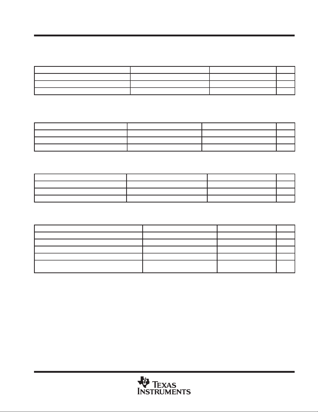
logic output SIMCLK in 5-V mode (according to GSM 11.11)
PARAMETER TEST CONDITIONS MIN TYP MAX UNIT
V
High-level output voltage (see Note 4) I
OH
V
Low-level output voltage (see Note 4) I
OL
tr/tfRise/fall time SIMCLK (see Note 5 and 6) Cin = C
NOTES: 4. For each state VOH, VOL, a positive current is defined as flowing out of the TSP9125.
5. T o allow for overshoot the voltage on SIMCLK should remain between –0.3 V and SIMVCC+0.3 V during dynamic operations.
6. The maximum rise/fall time is 9% of the SIMCLK period.
logic output SIMRST in 3-V mode (according to GSM 11.12)
PARAMETER TEST CONDITIONS MIN TYP MAX UNIT
V
High-level output voltage (see Note 4) I
OH
V
Low-level output voltage (see Note 4) I
OL
tr/tfRise/fall time SIMRST (see Note 5) Cin = C
NOTES: 4. For each state VOH, VOL, a positive current is defined as flowing out of the TSP9125.
5. T o allow for overshoot the voltage on SIMCLK should remain between –0.3 V and SIMVCC+0.3 V during dynamic operations.
= 1 µF ±20%; SIMPWR = 1 (unless otherwise noted) (continued)
= 20 µA 0.7×SIMV
OHmax
= –200 µA 0 0.5 V
OLmax
= 100 pF, f
out
= 200 µA 0.8×SIMV
OHmax
= –200 µA 0 0.2×SIMV
OLmax
= 100 pF 400 µs
out
= 5 MHz 18 ns
SIMCLK
CC
CC
SIMV
SIMV
CC
CC
CC
V
V
V
logic output SIMRST in 5-V mode (according to GSM 11.11)
PARAMETER TEST CONDITIONS MIN TYP MAX UNIT
V
High-level output voltage (see Note 4) I
OH
V
Low-level output voltage (see Note 4) I
OL
tr/tfRise/fall time SIMRST (see Note 5) Cin = C
NOTES: 4. For each state VOH, VOL, a positive current is defined as flowing out of the TSP9125.
5. T o allow for overshoot the voltage on SIMCLK should remain between –0.3 V and SIMVCC+0.3 V during dynamic operations.
= 200 µA SIMVCC–0.7V SIMV
OHmax
= –200 µA 0 0.6 V
OLmax
= 100 pF 400 µs
out
CC
V
logic input/output DATA
PARAMETER TEST CONDITIONS MIN TYP MAX UNIT
V
High-level input voltage on DATA (see Note 7) 0.7×V
IH
V
Low-level input voltage on DATA (see Note 7) 0.2×V
IL
V
High-level output voltage on DATA (see Note 7) I
OH
V
Low-level output voltage on DATA (see Note 7) I
OL
tr/tfRise/fall time DA TA (see Note 5)
NOTES: 5. To allow for overshoot the voltage on SIMCLK should remain between –0.3 V and SIMVCC+0.3 V during dynamic operations.
7. For each state VOH, VOL, VIH, VIL, a positive current is defined as flowing out of the TSP9125.
Cin = C
Integrated pullup resistor = 20 kΩ
OHmax
OLmax
= 20 µA, V
= –1 mA, V
= 100 pF,
out
SIMDATA
SIMDATA
= 3 V 0.7×V
= 0 V 0 0.4 V
DD
DD
DD
V
DD
1 µs
V
V
V
POST OFFICE BOX 655303 • DALLAS, TEXAS 75265
7
TPS9125
Ground current, operating
A
5 V/3 V SIM SUPPLY AND LEVEL SHIFTERS
SLVS244A – SEPTEMBER 1999 – REVISED NOVEMBER 1999
electrical characteristics over recommended operating junction temperature range, VDD = 3 V,
C
VCAP1/2
= 220 nF ±20%; C
SIMVCC
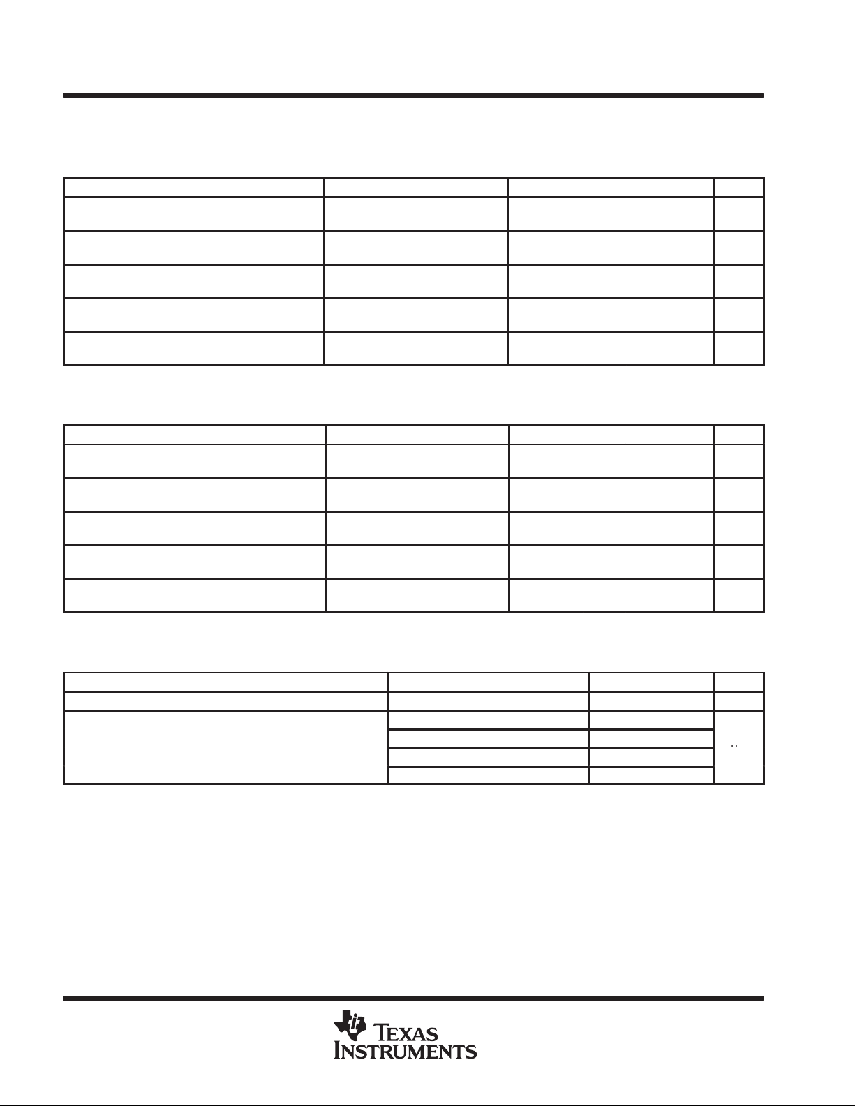
logic input/output SIMDATA in 3-V mode (according to GSM 11.12)
PARAMETER TEST CONDITIONS MIN TYP MAX UNIT
High-level input voltage on SIMDATA
V
IH
(see Note 7)
Low-level input voltage on SIMDATA (see
V
IL
Note 7)
High-level output voltage on SIMDATA
V
OH
(see Note 7)
Low-level output voltage on SIMDATA
V
OL
(see Note 7)
tr/tfRise/fall time SIMRST (see Note 5)
NOTES: 5. To allow for overshoot the voltage on SIMCLK should remain between –0.3 V and SIMVCC+0.3 V during dynamic operations.
7. For each state VOH, VOL, VIH, VIL, a positive current is defined as flowing out of the TSP9125.
logic input/output SIMDATA in 5-V mode (according to GSM 11.12)
PARAMETER TEST CONDITIONS MIN TYP MAX UNIT
High-level input voltage on SIMDATA (see
V
IH
Note 7)
Low-level input voltage on SIMDATA (see
V
IL
Note 7)
High-level output voltage on SIMDATA
V
OH
(see Note 7)
Low-level output voltage on SIMDATA
V
OL
(see Note 7)
tr/tfRise/fall time SIMRST (see Note 5)
NOTES: 5. To allow for overshoot the voltage on SIMCLK should remain between –0.3 V and SIMVCC+0.3 V during dynamic operations.
7. For each state VOH, VOL, VIH, VIL, a positive current is defined as flowing out of the TSP9125.
= 1 µF ±20%; SIMPWR = 1 (unless otherwise noted) (continued)
I
= ±20 µA 0.7×SIMV
IHmax
I
= 1 mA –0.3 0.2×SIMV
ILmax
I
= 20 µA, V
OHmax
I
= –1 mA, V
OLmax
Cin = C
Integrated pullup resistor = 10 kΩ
I
IHmax
I
ILmax
I
OHmax
I
OLmax
Cin = C
Integrated pullup resistor = 10 kΩ
= 100 pF,
out
= ±20 µA 0.7×SIMV
= 1 mA –0.3 0.8 V
= 20 µA, V
= –1 mA, V
= 100 pF,
out
= 3 V 0.7×SIMV
DATA
= 0 V 0 0.4 V
DATA
= 3 V 0.7×SIMV
DATA
= 0 V 0 0.4 V
DATA
CC
CC
CC
CC
SIMVCC+0.3V V
CC
SIMV
CC
1 µs
SIMVCC+0.3V V
SIMV
CC
1 µs
V
V
V
supply current
PARAMETER TEST CONDITIONS MIN TYP MAX UNIT
Powerdown/programming mode SIMPWR = 0 5 µA
SIMVCC = 5 V, I
p
SIMVCC = 5 V, I
SIMVCC = 3 V, I
SIMVCC = 3 V, I
SIMVCC
SIMVCC
SIMVCC
SIMVCC
= 0 mA 125
= 10 mA 200
= 0 mA 25
= 6 mA 40
µ
8
POST OFFICE BOX 655303 • DALLAS, TEXAS 75265
 Loading...