

Texas Instruments TPS73001DBVR, TPS73018DBVR, TPS73018YZQR, TPS73025DBVR, TPS73025YZQR Schematic [ru]
...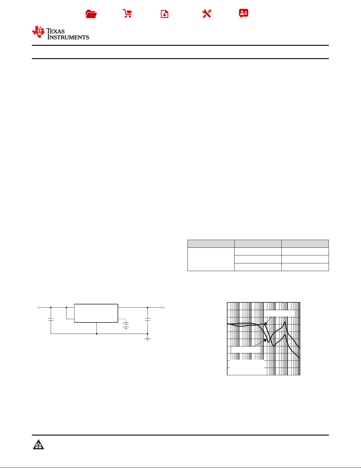
10 100 1 k 10 k
10
40
80
100 k 1 M 10 M
Ripple Rejection (dB)
Frequency (Hz)
I
OUT
= 10 mA
50
0
VIN= 3.8 V
C
OUT
= 10 Fm
CNR= 0.01 Fm
I
OUT
= 200 mA
20
30
60
70
90
100
TPS730xx
GNDEN NR
IN OUT
V
IN
V
OUT
V
IN
V
OUT
2.2µF
0.01µF
(1)
0.1µF
NOTE: (1) This capacitor isoptional.
Product
Folder
Sample &
Buy
Technical
Documents
Tools &
Software
Support &
Community
SBVS054J –NOVEMBER 2004–REVISED APRIL 2015
TPS730 Low-Noise, High PSRR, RF, 200-mA Low-Dropout Linear Regulators
1 Features 3 Description
1
• 200-mA RF Low-Dropout Regulator
With Enable
• Available in Fixed Voltages from 1.8 V to 3.3 V
and Adjustable Voltages (1.22 V to 5.5 V)
• High PSRR (68 dB at 100 Hz)
• Low Noise (33 μV
, TPS73018)
RMS
• Fast Start-Up Time (50 μs)
• Stable With a 2.2-μF Ceramic Capacitor
• Excellent Load/Line Transient Response
• Very Low Dropout Voltage (120 mV at 200 mA)
• 5- and 6-Pin SOT-23 (DBV), and Wafer Chip
Scale (YZQ) Packages
2 Applications
• RF: VCOs, Receivers, ADCs
• Audio
• Cellular and Cordless Telephones
• Bluetooth®, Wireless LAN
• Handheld Organizers, PDAs
The TPS730 family of low-dropout (LDO) low-power
linear voltage regulators features high power-supply
rejection ratio (PSRR), low noise, fast start-up, and
excellent line and load transient responses in a small
SOT-23 package. NanoStar™ packaging gives an
ultrasmall footprint as well as an ultralow profile and
package weight, making it ideal for portable
applications such as handsets and PDAs. Each
device in the family is stable, with a small, 2.2-μF
ceramic capacitor on the output. The TPS730 family
uses an advanced, proprietary BiCMOS fabrication
process to yield low dropout voltages (for example,
120 mV at 200 mA, TPS73030). Each device
achieves fast start-up times (approximately 50 μs with
a 0.001-μF bypass capacitor) while consuming low
quiescent current (170 μA typical). Moreover, when
the device is placed in standby mode, the supply
current is reduced to less than 1 μA. The TPS73018
exhibits approximately 33 μV
noise at 1.8 V output with a 0.01-μF bypass
capacitor. Applications with analog components that
are noise-sensitive, such as portable RF electronics,
benefit from the high PSRR and low-noise features
as well as the fast response time.
of output voltage
RMS
TPS730
Device Information
(1)
PART NUMBER PACKAGE BODY SIZE (NOM)
SOT-23 (5) 2.90 mm × 1.60 mm
TPS730 SOT-23 (6) 2.90 mm × 1.60 mm
DSBGA (5) 1.35 mm × 1.00 mm
(1) For all available packages, see the orderable addendum at
the end of the data sheet.
Simplified Schematic Ripple Rejection vs Frequency
1
An IMPORTANT NOTICE at the end of this data sheet addresses availability, warranty, changes, use in safety-critical applications,
intellectual property matters and other important disclaimers. PRODUCTION DATA.
TPS730
SBVS054J –NOVEMBER 2004–REVISED APRIL 2015
www.ti.com
Table of Contents
1 Features.................................................................. 1
2 Applications ........................................................... 1
3 Description ............................................................. 1
4 Revision History..................................................... 2
5 Pin Configuration and Functions......................... 3
6 Specifications......................................................... 4
6.1 Absolute Maximum Ratings ...................................... 4
6.2 ESD Ratings ............................................................ 4
6.3 Recommended Operating Conditions....................... 4
6.4 Thermal Information.................................................. 4
6.5 Electrical Characteristics .......................................... 5
6.6 Typical Characteristics.............................................. 6
7 Detailed Description.............................................. 9
7.1 Overview ................................................................... 9
7.2 Functional Block Diagrams ....................................... 9
7.3 Feature Description................................................. 10
7.4 Device Functional Modes........................................ 10
8 Application and Implementation ........................ 11
8.1 Application Information............................................ 11
8.2 Typical Application .................................................. 13
8.3 Do's and Don'ts....................................................... 14
9 Power Supply Recommendations...................... 15
10 Layout................................................................... 15
10.1 Layout Guidelines ................................................. 15
10.2 Layout Example .................................................... 15
10.3 Thermal Considerations........................................ 16
10.4 Power Dissipation ................................................. 16
11 Device and Documentation Support................. 18
11.1 Device Support...................................................... 18
11.2 Documentation Support ........................................ 18
11.3 Trademarks ........................................................... 18
11.4 Electrostatic Discharge Caution............................ 18
11.5 Glossary ................................................................ 18
12 Mechanical, Packaging, and Orderable
Information........................................................... 18
12.1 TPS730YZQ Nanostar™ Wafer Chip Scale
Information............................................................... 19
4 Revision History
NOTE: Page numbers for previous revisions may differ from page numbers in the current version.
Changes from Revision I (February, 2011) to Revision J Page
• Added ESD Ratings table, Feature Description section, Device Functional Modes, Application and Implementation
section, Power Supply Recommendations section, Layout section, Device and Documentation Support section, and
Mechanical, Packaging, and Orderable Information section ................................................................................................. 1
• Changed fourth bullet of Features list to low noise ............................................................................................................... 1
• Changed front-page figure ..................................................................................................................................................... 1
• Added Pin Configuration and Functions section .................................................................................................................... 3
• Changed "free-air temperature" to "junction temperature" in Absolute Maximum Ratings condition statement ................... 4
• Deleted Dissipation Ratings table; added Thermal Information table ................................................................................... 4
• Added condition statement to Typical Characteristics ........................................................................................................... 6
• Moved Ordering Information to Device Nomenclature section ............................................................................................ 18
Changes from Revision H (October, 2007) to Revision I Page
• Corrected units in y-axis of Figure 5....................................................................................................................................... 6
2 Submit Documentation Feedback Copyright © 2004–2015, Texas Instruments Incorporated
Product Folder Links: TPS730
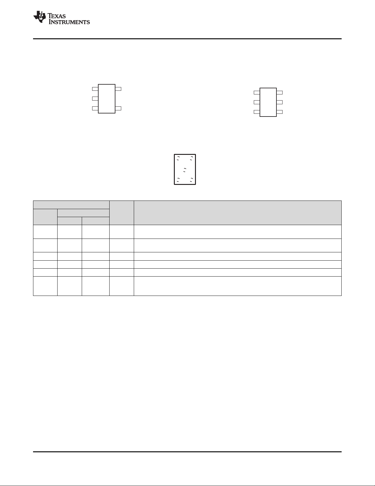
A3 A1
C3 C1
B2
IN
OUT
GND
NR
EN
3
2
4
5
6
1
GND
OUT
NR
FB
EN
IN
Adjustable Voltage Version
3
2
4
5
1
GND
OUT
NREN
IN
Fixed Voltage Versions
www.ti.com
5 Pin Configuration and Functions
TPS730
SBVS054J –NOVEMBER 2004–REVISED APRIL 2015
DBV Package
5-Pin SOT-23
Top View
DBV Package
6-Pin SOT-23
Top View
YZQ Package
5-Pin DSBGA
Top View
Pin Functions
PIN
NAME
EN 3 A3 I
FB 5 N/A I
GND 2 A1 — Regulator ground.
IN 1 C3 I Input to the device.
OUT 6 C1 O Output of the regulator.
NR 4 B2 — the internal bandgap. This configuration improves power-supply rejection and reduces output
NO. I/O DESCRIPTION
SOT-23 DSBGA
Enable pin. Driving the enable pin (EN) high turns on the regulator. Driving this pin low puts
the regulator into shutdown mode. EN can be connected to IN if not used.
Feedback pin. This terminal is the feedback input pin for the adjustable device. Fixed-voltage
versions in the DBV package do not have this pin.
Noise Reduction pin. Connecting an external capacitor to this pin filters noise generated by
noise.
Copyright © 2004–2015, Texas Instruments Incorporated Submit Documentation Feedback 3
Product Folder Links: TPS730
TPS730
SBVS054J –NOVEMBER 2004–REVISED APRIL 2015
www.ti.com
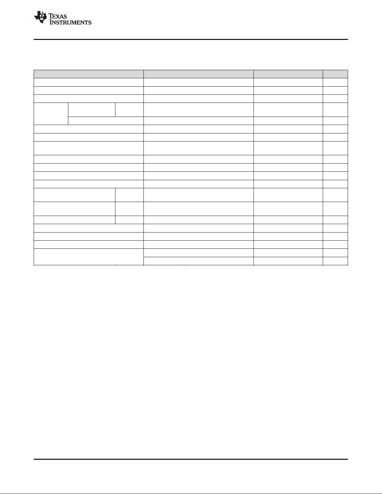
6 Specifications
6.1 Absolute Maximum Ratings
over operating junction temperature range (unless otherwise noted)
Input range, V
Voltage Enable range, V
Output range, V
Current Peak output, I
Continuous total power dissipation See Thermal Information
Temperature YZQ package –40 125 °C
Junction, T
Storage, T
(1) Stresses beyond those listed under Absolute Maximum Ratings may cause permanent damage to the device. These are stress ratings
only, which do not imply functional operation of the device at these or any other conditions beyond those indicated under Recommended
Operating Conditions. Exposure to absolute-maximum-rated conditions for extended periods may affect device reliability.
IN
EN
OUT
OUT(max)
DBV package –40 150
J
stg
6.2 ESD Ratings
Human body model (HBM), per ANSI/ESDA/JEDEC JS-001, all pins
V
(1) JEDEC document JEP155 states that 500-V HBM allows safe manufacturing with a standard ESD control process.
(2) JEDEC document JEP157 states that 250-V CDM allows safe manufacturing with a standard ESD control process.
Electrostatic discharge V
(ESD)
Charged device model (CDM), per JEDEC specification JESD22-C101,
(2)
all pins
(1)
MIN MAX UNIT
–0.3 6
–0.3 6 V
–0.3 6
Internally limited
–65 150
VALUE UNIT
(1)
±2000
±500
6.3 Recommended Operating Conditions
over operating junction temperature range (unless otherwise noted).
MIN NOM MAX UNIT
V
IN
V
EN
V
OUT
I
OUT
T
J
C
IN
C
OUT
C
NR
C
FF
R
2
(1) If CFFis not used or V
Input supply voltage 2.7 5.5 V
Enable supply voltage 0 V
Output voltage V
FB
IN
5 V
V
Output current 0 200 mA
Operating junction temperature –40 125 °C
Input capacitor 0.1 1 µF
Output capacitor 2.2
(1)
10 µF
Noise reduction capacitor 0 10 nF
Feed-forward capacitor 15 pF
Lower feedback resistor 30.1 kΩ
OUT(nom)
< 1.8 V, the minimum recommended C
OUT
= 4.7 µF.
6.4 Thermal Information
TPS73001
THERMAL METRIC
R
θJA
R
θJC(top)
R
θJB
ψ
JT
ψ
JB
Junction-to-ambient thermal resistance 225.1 178.5
Junction-to-case (top) thermal resistance 78.4 1.4
Junction-to-board thermal resistance 54.7 62.1 °C/W
Junction-to-top characterization parameter 3.3 0.9
Junction-to-board characterization parameter 53.8 62.1
(1) For more information about traditional and new thermal metrics, see the IC Package Thermal Metrics application report, SPRA953.
(1)
DBV (SOT-23) YZQ (DSBGA) UNIT
6 PINS 5 PINS
4 Submit Documentation Feedback Copyright © 2004–2015, Texas Instruments Incorporated
Product Folder Links: TPS730
www.ti.com
SBVS054J –NOVEMBER 2004–REVISED APRIL 2015
6.5 Electrical Characteristics
Over recommended operating temperature range TJ= –40 to +125°C, VEN= VIN, VIN= V
10 μF, CNR= 0.01 μF (unless otherwise noted). Typical values are at 25°C.
PARAMETER TEST CONDITIONS MIN TYP MAX UNIT
V
I
OUT
V
IN
FB
Input voltage range
Continuous output current 0 200 mA
Internal reference (TPS73001) 1.201 1.225 1.25 V
Output voltage
V
OUT
range
Output voltage accuracy 0 µA ≤ I
ΔV
OUT(ΔVIN)
ΔV
OUT(ΔIOUT)
V
DO
I
CL
I
GND
I
SHUTDOWN
I
FB
PSRR TPS73028 f = 100 Hz, I
V
n
t
STR
V
EN(high)
V
EN(low)
I
EN
Line regulation
Load regulation 0 µA ≤ I
Dropout voltage
(VIN= V
OUT(nom)
Output current limit V
Ground pin current 0 µA < I
Shutdown current
FB pin current VFB= 1.8 V 1 μA
Power-supply
rejection ratio
Output noise BW = 200 Hz to 100 kHz, I
voltage CNR= 0.01 μF
Start-up time TPS73018 RL= 14 Ω, C
High-level enable input voltage 2.7 V ≤ VIN≤ 5.5 V 1.7 V
Low-level enable input voltage 2.7 V ≤ VIN≤ 5.5 V 0 0.7 V
EN pin current VEN= 0 V –1 1 μA
UVLO
(1) Minimum VINis 2.7 V or V
(2) Dropout is not measured for the TPS73018 and TPS73025 since minimum VIN= 2.7 V.
(3) For adjustable versions, this applies only after VINis applied; then VENtransitions high to low.
(1)
TPS73001 V
≤ 200 mA, 2.75 V ≤ VIN≤ 5.5 V –2% V
(1)
(2)
– 0.1 V)
(3)
TPS73018 33 μV
OUT
V
+ 1 V ≤ VIN≤ 5.5 V 0.05 %/V
OUT
≤ 200 mA, TJ= 25°C 5 mV
OUT
I
= 200 mA 120 210 mV
OUT
= 0 V 285 600 mA
OUT
< 200 mA 170 250 μA
OUT
VEN= 0 V, 2.7 V ≤ VIN≤ 5.5 V 0.07 1 μA
= 200 mA, TJ= 25°C 68 dB
OUT
= 200 mA,
OUT
= 1 µF, CNR= 0.001 μF 50 μs
OUT
Threshold, VCCrising 2.25 2.65 V
Hysteresis 100 mV
+ VDO, whichever is greater.
OUT
(1)
+ 1 V
OUT(nom)
, I
OUT
2.7 5.5 V
FB
5.5 – V
OUT(nom)
TPS730
= 1 mA, C
DO
2% V
IN
OUT
V
V
=
RMS
Copyright © 2004–2015, Texas Instruments Incorporated Submit Documentation Feedback 5
Product Folder Links: TPS730
0
20
40
60
80
100
120
140
160
180
−40 −25−10 5 20 35 50 65 80 95 110 125
I
OUT
= 200 mA
I
OUT
= 10 mA
VIN= 2.7 V
C
OUT
= 10 Fm
TJ(°C)
V
DO
(mV)
60
50
40
30
20
10
0
RMS Output Noise ( V )m
RMS
0.001 0.01 0.1
C ( F)m
NR
BW = 100 Hz to 100 kHz
V = 2.8 V
I = 200 mA
C = 10 F
OUT
OUT
OUT
m
0
50
100
150
200
250
−40 −25−10 5 20 35 50 65 80 95 110 125
TJ(°C)
I
OUT
= 1 mA
VIN= 3.8 V
C
OUT
= 10 Fm
I
OUT
= 200 mA
I
GND
(mA)
0
0.2
0.4
0.6
0.8
1.0
1.2
1.4
1.6
100 1 k 10 k 100 k
Frequency (Hz)
VIN= 3.8 V
I
OUT
= 200 mA
C
OUT
= 10 Fm
CNR= 0.1 Fm
CNR= 0.001 Fm
CNR= 0.0047 Fm
CNR= 0.01 Fm
Output Spectral Noise Density (
mV/ Hz√
)
2.795
2.796
2.797
2.798
2.799
2.800
2.801
2.802
2.803
2.804
2.805
0 50 100 150 200
I
OUT
(mA)
VIN= 3.8 V
C
OUT
= 10 Fm
TJ= 25 C°
V
OUT
(V)
2.775
2.780
2.785
2.790
2.795
2.800
2.805
−40 −25−10 5 20 35 50 65 80 95 110 125
TJ(°C)
I
OUT
= 200 mA
I
OUT
= 1 mA
VIN= 3.8 V
C
OUT
= 10 Fm
V
OUT
(V)
TPS730
SBVS054J –NOVEMBER 2004–REVISED APRIL 2015
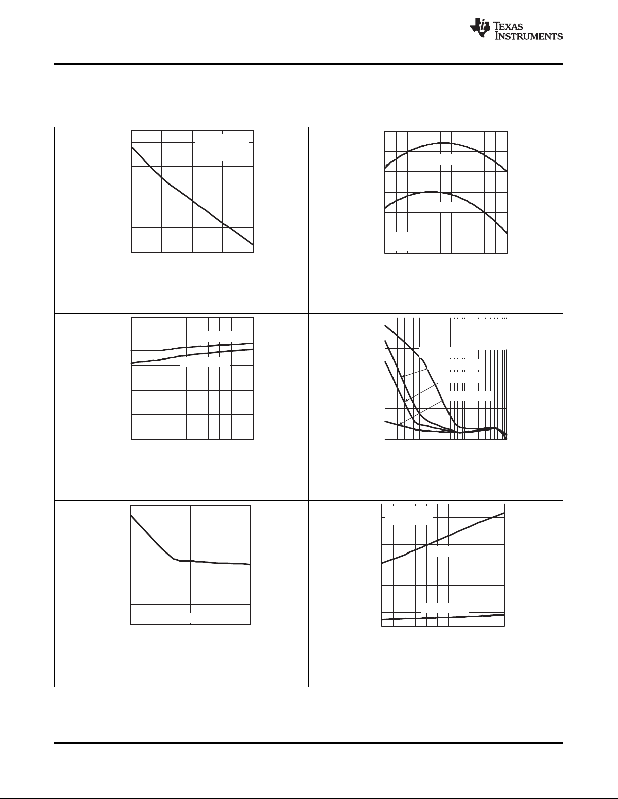
6.6 Typical Characteristics
Over recommended operating temperature range TJ= –40°C to +125°C, VEN= VIN, VIN= V
10 μF, CNR= 0.01 μF, V
Figure 1. TPS73028 Output Voltage vs Output Current Figure 2. TPS73028 Output Voltage vs Junction
OUT(nom)
= 2.8 V (unless otherwise noted). Typical values are at TJ= 25°C.
OUT(nom)
+ 1 V, I
Temperature
= 1 mA, C
OUT
www.ti.com
OUT
=
Figure 3. TPS73028 Ground Current vs Junction Figure 4. TPS73028 Output Spectral Noise Density vs
6 Submit Documentation Feedback Copyright © 2004–2015, Texas Instruments Incorporated
Figure 5. Root Mean Square Output Noise vs C
Temperature Frequency
NR
Figure 6. TPS73028 Dropout Voltage vs Junction
Temperature
Product Folder Links: TPS730
100
50
0 20 40 60 80 100 120
150
200
250
140 160 180 200
0
I
OUT
(mA)
TJ= 125 C°
TJ= 25 C°
TJ= −55 C°
V
DO
(mV)
500 mV/div
1s/div
V
IN
V
OUT
V
OUT
= 3 V
RL= 15 W
Time (ms)
0 302010 40 50 7060 80 90 100
I
OUT
= 200 mA
C
OUT
= 2.2 Fm
CNR= 0.01 Fm
0
-20
3.8
dv
dt
0.4 V
ms
20
4.8
V
IN
(mV)
V
OUT
(mV)
=
Time (ms)
0
0 15010050 200 250 350300 400 450
20
0
−20
100
500
VIN= 3.8 V
C
OUT
= 10 Fm
−40
200
300
di
dt
0.02A
ms
1mA
I
OUT
(mA)
DV
OUT
(mV)
=
10 100 1 k 10 k
10
40
80
100 k 1 M 10 M
Ripple Rejection (dB)
Frequency (Hz)
I
OUT
= 10 mA
50
0
VIN= 3.8 V
C
OUT
= 10 Fm
CNR= 0.01 Fm
I
OUT
= 200 mA
20
30
60
70
90
100
3
Time (ms)
0 604020 80 100 140120 160 180 200
VIN= 3.8 V
V
OUT
= 2.8 V
I
OUT
= 200 mA
C
OUT
= 2.2 Fm
TJ= 25 C°
1
2
0
0
2
CNR= 0.0047 Fm
CNR= 0.01 Fm
4
CNR= 0.001 Fm
V
EN
(V)
V
OUT
(V)
www.ti.com
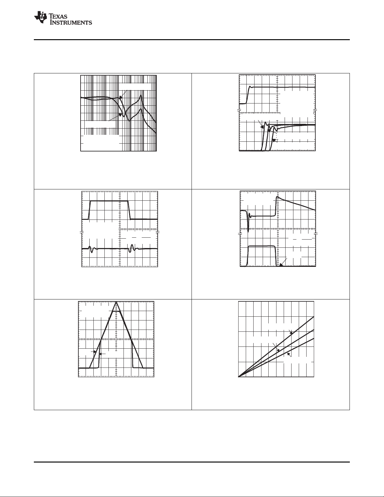
Typical Characteristics (continued)
TPS730
SBVS054J –NOVEMBER 2004–REVISED APRIL 2015
Over recommended operating temperature range TJ= –40°C to +125°C, VEN= VIN, VIN= V
10 μF, CNR= 0.01 μF, V
Figure 7. TPS73028 Ripple Rejection vs Frequency Figure 8. TPS73028 Output Voltage, Enable Voltage vs Time
OUT(nom)
= 2.8 V (unless otherwise noted). Typical values are at TJ= 25°C.
OUT(nom)
(Start-Up)
+ 1 V, I
= 1 mA, C
OUT
OUT
=
Figure 9. TPS73028 Line Transient Response
Copyright © 2004–2015, Texas Instruments Incorporated Submit Documentation Feedback 7
Figure 11. Power Up and Power Down
Figure 10. TPS73028 Load Transient Response
Figure 12. Dropout Voltage vs Output Current
Product Folder Links: TPS730
0.01
0.1
10
100
0 0.02 0.04 0.06 0.08 0.20
I
OUT
(A)
1
Region of Instability
Region of Stability
C
OUT
= 2.2 µF
VIN = 5.5 V, V
OUT
≥ 1.5 V
TJ = −40°C to 125°C
ESR, Equivalent Series Resistance (Ω)
0.01
0.1
10
100
0 0.02 0.04 0.06 0.08
0.20
I
OUT
(A)
1
Region of Instability
Region of Stability
C
OUT
= 10 µF
VIN = 5.5 V
TJ = −40°C to 125°C
ESR, Equivalent Series Resistance (Ω)
TPS730
SBVS054J –NOVEMBER 2004–REVISED APRIL 2015
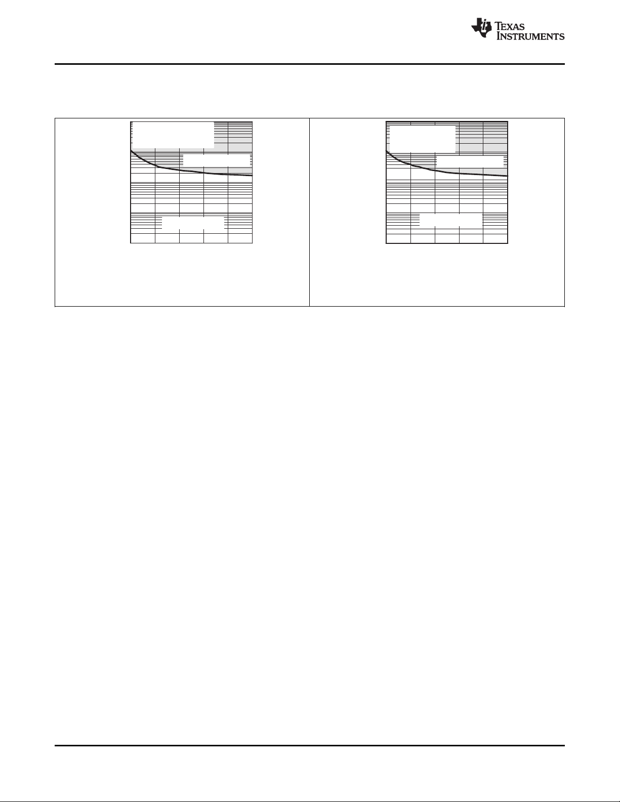
Typical Characteristics (continued)
www.ti.com
Over recommended operating temperature range TJ= –40°C to +125°C, VEN= VIN, VIN= V
10 μF, CNR= 0.01 μF, V
OUT(nom)
= 2.8 V (unless otherwise noted). Typical values are at TJ= 25°C.
OUT(nom)
+ 1 V, I
OUT
Figure 13. Typical Regions of Stability Equivalent Series Figure 14. Typical Regions of Stability Equivalent Series
Resistance (ESR) vs Output Current Resistance (ESR) vs Output Current
= 1 mA, C
OUT
=
8 Submit Documentation Feedback Copyright © 2004–2015, Texas Instruments Incorporated
Product Folder Links: TPS730
_
+
Thermal
Shutdown
Current
Sense
R1
R2
GND
EN
SHUTDOWN
V
ref
UVLO
ILIM
250 kW
NR
QuickStart
Bandgap
Reference
1.22V
UVLO
2.45V
R2 = 40 kW
IN
IN OUT
_
+
Thermal
Shutdown
Bandgap
Reference
1.22V
Current
Sense
R2
GND
EN
SHUTDOWN
V
ref
UVLO
ILIM
External to
the Device
R1
UVLO
2.45V
250 kW
NR
FB
59 k
QuickStart
OUTIN
IN
TPS730
www.ti.com
SBVS054J –NOVEMBER 2004–REVISED APRIL 2015
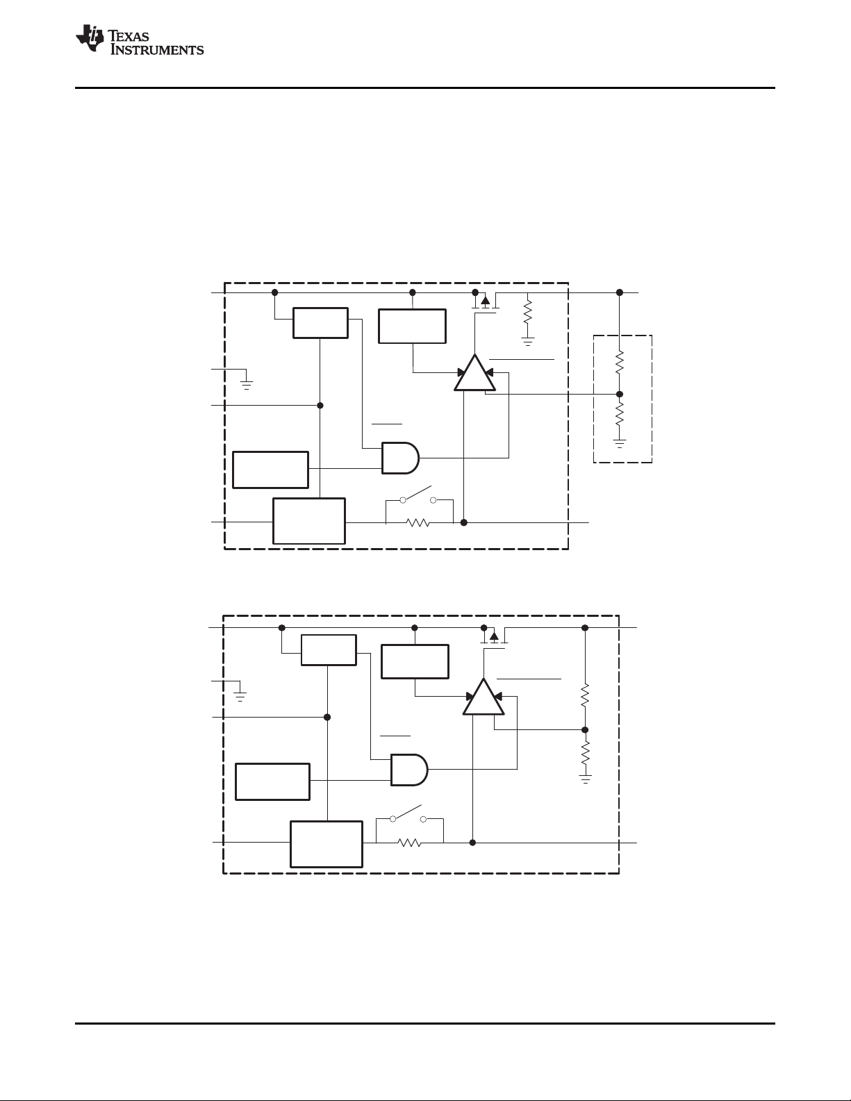
7 Detailed Description
7.1 Overview
The TPS730 family of low-dropout (LDO) regulators has been optimized for use in noise-sensitive, batteryoperated equipment. The device features extremely low dropout voltages, high PSRR, ultra-low output noise, low
quiescent current (170 μA typically), and enable-input to reduce supply currents to less than 1 μA when the
regulator is turned off.
7.2 Functional Block Diagrams
Figure 15. TPS730 Block Diagram (Adjustable-Voltage Version)
Copyright © 2004–2015, Texas Instruments Incorporated Submit Documentation Feedback 9
Figure 16. TPS730 Block Diagram (Fixed-Voltage Versions)
Product Folder Links: TPS730
TPS730
SBVS054J –NOVEMBER 2004–REVISED APRIL 2015
www.ti.com
7.3 Feature Description
7.3.1 Undervoltage Lockout (UVLO)
The TPS730 uses an undervoltage lockout (UVLO) circuit that disables the output until the input voltage is
greater than the rising UVLO voltage. This circuit ensures that the device does not exhibit any unpredictable
behavior when the supply voltage is lower than the operational range of the internal circuitry, V
IN(min)
.
7.3.2 Shutdown
The enable pin (EN) is active high. Enable the device by forcing the EN pin to exceed V
(1.7 V, minimum).
EN(high)
Turn off the device by forcing the EN pin to drop below 0.7 V. If shutdown capability is not required, connect EN
to IN.
7.3.3 Foldback Current Limit
The TPS730 features internal current limiting and thermal protection. During normal operation, the TPS730 limits
output current to approximately 400 mA. When current limiting engages, the output voltage scales back linearly
until the overcurrent condition ends. While current limiting is designed to prevent gross device failure, do not
exceed the power dissipation ratings of the package or the absolute maximum voltage ratings of the device.
7.4 Device Functional Modes
7.4.1 Normal Operation
The device regulates to the nominal output voltage under the following conditions:
• The input voltage is at least as high as V
• The input voltage is greater than the nominal output voltage added to the dropout voltage.
• The enable voltage is greater than V
EN(min)
• The output current is less than the current limit.
• The device junction temperature is less than the maximum specified junction temperature.
IN(min)
.
.
7.4.2 Dropout Operation
If the input voltage is lower than the nominal output voltage plus the specified dropout voltage, but all other
conditions are met for normal operation, the device operates in dropout mode. In this mode of operation, the
output voltage is the same as the input voltage minus the dropout voltage. The transient performance of the
device is significantly degraded because the pass device is in the linear region and no longer controls the current
through the LDO. Line or load transients in dropout can result in large output voltage deviations.
7.4.3 Disabled
The device is disabled under the following conditions:
• The enable voltage is less than the enable falling threshold voltage or has not yet exceeded the enable rising
threshold.
• The device junction temperature is greater than the thermal shutdown temperature.
• The input voltage is less than UVLO
falling
.
Table 1 shows the conditions that lead to the different modes of operation.
Table 1. Device Functional Mode Comparison
OPERATING MODE
Normal mode VEN> V
Dropout mode V
Disabled mode
(any true condition disables the VIN< UVLO
device)
(1) Approximate value for thermal shutdown.
VIN> V
IN(min)
V
OUT(nom)
VIN> V
< VIN< V
IN
+ VDOand
IN(min)
OUT(nom)
falling
+ V
DO
V
VEN> V
VEN< V
PARAMETER
EN
EN(high)
EN(high)
EN(low)
I
OUT
I
< I
OUT
LIM
— TJ< 125°C
— TJ> 165°C
TJ< 125°C
T
J
(1)
10 Submit Documentation Feedback Copyright © 2004–2015, Texas Instruments Incorporated
Product Folder Links: TPS730

GNDNR
FB
IN OUT
EN
V
IN
V
OUT
R
1
C
1
R
2
1 Fm
2.2 Fm
0.01 Fm
TPS73001
OUTPUTVOLTAGE
PROGRAMMINGGUIDE
R
1
R
2
C
1
2.5V
3.3V
3.6V
1.22V
OUTPUT
VOLTAGE
31.6kW
short
51kW
59kW
open
30.1kW
30.1kW
30.1kW
0pF
22pF
15pF
15pF
7
1 2
1
(3 10 ) (R R )
C
(R R )
u u
u
R =
1
- 1 ´ R
2
V
OUT
V
REF
1
O U T R E F
2
R
V V 1
R
§ ·
u
¨ ¸
© ¹
TPS730
www.ti.com
SBVS054J –NOVEMBER 2004–REVISED APRIL 2015
8 Application and Implementation
NOTE
Information in the following applications sections is not part of the TI component
specification, and TI does not warrant its accuracy or completeness. TI’s customers are
responsible for determining suitability of components for their purposes. Customers should
validate and test their design implementation to confirm system functionality.
8.1 Application Information
The TPS730 family of low-dropout (LDO) regulators has been optimized for use in noise-sensitive batteryoperated equipment. The device features extremely low dropout voltages, high PSRR, ultra-low output noise, low
quiescent current (170 μA typically), and enable-input to reduce supply currents to less than 1 μA when the
regulator is turned off.
8.1.1 Adjustable Operation
The output voltage of the TPS73001 adjustable regulator is programmed using an external resistor divider as
shown in Figure 17. The output voltage is calculated using Equation 1:
Where:
• V
Resistors R1and R2should be chosen for approximately 50-μA divider current. Lower value resistors can be
used for improved noise performance, but the solution consumes more power. Higher resistors values can cause
accuracy issues and other problems. The recommended design procedure is to choose R2= 30.1 kΩ to set the
divider current at 50 μA, C1= 15 pF for stability, and then calculate R1using Equation 2:
= 1.225 V typical (the internal reference voltage) (1)
REF
To improve the stability of the adjustable version, TI suggests placing a small compensation capacitor between
OUT and FB. For output voltages < 1.8 V, the value of this capacitor should be 100 pF. For output voltages > 1.8
V, use Equation 3 to calculate the approximate value of this capacitor.
Figure 17 shows the suggested value of this capacitor for several resistor ratios. If this capacitor is not used
(such as in a unity-gain configuration) or if an output voltage < 1.8 V is chosen, then the minimum recommended
output capacitor is 4.7 μF instead of 2.2 μF.
Copyright © 2004–2015, Texas Instruments Incorporated Submit Documentation Feedback 11
Figure 17. TPS73001 Adjustable LDO Regulator Programming
Product Folder Links: TPS730
(2)
(3)

TPS730
SBVS054J –NOVEMBER 2004–REVISED APRIL 2015
www.ti.com
Application Information (continued)
8.1.2 Capacitor Recommendations
Low equivalent series resistance (ESR) capacitors should be used for the input, output, noise reduction, and
bypass capacitors. Ceramic capacitors with X7R and X5R dielectrics are preferred. These dielectrics offer more
stable characteristics. Ceramic X7R capacitors offer improved overtemperature performance, while ceramic X5R
capacitors are more cost-effective and are available in higher values.
8.1.3 Input and Output Capacitor Requirements
A 0.1-μF or larger ceramic input bypass capacitor, connected between IN and GND and located close to the
TPS730, is required for stability and improves transient response, noise rejection, and ripple rejection. A highervalue input capacitor may be necessary if large, fast-rise-time load transients are anticipated or the device is
located several inches from the power source.
Like most low-dropout regulators, the TPS730 requires an output capacitor connected between OUT and GND to
stabilize the internal control loop. The minimum recommended capacitance is 2.2 μF. Any 2.2-μF or larger
ceramic capacitor is suitable, provided the capacitance does not vary significantly over temperature. If load
current is not expected to exceed 100 mA, a 1-μF ceramic capacitor can be used. If a feed-forward capacitor is
not used (such as in a unity-gain configuration) or if an output voltage less than 1.8 V is chosen, then the
minimum recommended output capacitor is 4.7 μF instead of 2.2 μF. Table 2 lists the recommended output
capacitor sizes for several common configurations.
Table 2. Output Capacitor Sizing
CONDITION C
V
< 1.8 V or CFF= 0 nF 4.7
OUT
V
V
OUT
OUT
> 1.8 V, I
> 1.8 V, I
> 100 mA 2.2
OUT
< 100 mA 1
OUT
OUT
(µF)
8.1.4 Noise Reduction and Feed-Forward Capacitor Requirements
The internal voltage reference is a key source of noise in an LDO regulator. The TPS730 has an NR pin which is
connected to the voltage reference through a 250-kΩ internal resistor. The 250-kΩ internal resistor, in
conjunction with an external bypass capacitor connected to the NR pin, creates a low-pass filter to reduce the
voltage reference noise and, therefore, the noise at the regulator output. In order for the regulator to operate
properly, the current flow out of the NR pin must be at a minimum, because any leakage current creates an IR
drop across the internal resistor thus creating an output error. Therefore, the bypass capacitor must have
minimal leakage current. The bypass capacitor should be no more than 0.1 μF to ensure that it is fully charged
during the quick-start time provided by the internal switch shown in the Functional Block Diagram section.
As an example, the TPS73018 exhibits only 33 μV
of output voltage noise using a 0.01-μF ceramic bypass
RMS
capacitor and a 2.2-μF ceramic output capacitor. Note that the output starts up slower as the bypass capacitance
increases due to the RC time constant at the NR pin that is created by the internal 250-kΩ resistor and external
capacitor.
A feed-forward capacitor is recommended to improve the stability of the device. If R2= 30.1 kΩ, set C1to 15 pF
for optimal performance. For voltages less than 1.8 V, the value of this capacitor should be 100 pF. For voltages
greater than 1.8 V, the approximate value of this capacitor can be calculated as shown in Equation 3.
8.1.5 Reverse Current Operation
The TPS730 PMOS-pass transistor has a built-in back diode that conducts reverse current when the input
voltage drops below the output voltage (for example, during power-down). Current is conducted from the output
to the input and is not internally limited. If extended reverse voltage operation is anticipated, external limiting
might be appropriate. If extended reverse voltage operation in anticipated, external limiting to 5% of the rated
output current is recommended.
12 Submit Documentation Feedback Copyright © 2004–2015, Texas Instruments Incorporated
Product Folder Links: TPS730

3
Time (ms)
0 604020 80 100 140120 160 180 200
VIN= 3.8 V
V
OUT
= 2.8 V
I
OUT
= 200 mA
C
OUT
= 2.2 Fm
TJ= 25 C°
1
2
0
0
2
CNR= 0.0047 Fm
CNR= 0.01 Fm
4
CNR= 0.001 Fm
V
EN
(V)
V
OUT
(V)
Time (ms)
0 302010 40 50 7060 80 90 100
I
OUT
= 200 mA
C
OUT
= 2.2 Fm
CNR= 0.01 Fm
0
-20
3.8
dv
dt
0.4 V
ms
20
4.8
V
IN
(mV)
V
OUT
(mV)
=
TPS730xx
GNDEN NR
IN OUT
V
IN
V
OUT
V
IN
V
OUT
2.2µF
0.01µF
(1)
0.1µF
NOTE: (1) This capacitoris optional.
www.ti.com
8.2 Typical Application
A typical application circuit is shown in Figure 18.
Figure 18. Typical Application Circuit
8.2.1 Design Requirements
Table 3 lists the design requirements.
Table 3. Design Parameters
PARAMETER DESIGN REQUIREMENT
Input voltage 4.2 V to 3 V (Lithium Ion battery)
Output voltage 1.8 V, ±1%
DC output current 10 mA
Peak output current 75 mA
Maximum ambient temperature 65°C
TPS730
SBVS054J –NOVEMBER 2004–REVISED APRIL 2015
8.2.2 Detailed Design Procedure
Pick the desired output voltage option. An input capacitor of 0.1 µF is used as the battery is connected to the
input through a via and a short 10-mil (0.01-in) trace. An output capacitor of 10 µF is used to provide optimal
response time for the load transient. Verify that the maximum junction temperature is not exceed by referring to
Figure 24.
8.2.3 Application Curves
Figure 19. TPS73028 Output Voltage, Enable Voltage vs Figure 20. TPS73028 Line Transient Response
Copyright © 2004–2015, Texas Instruments Incorporated Submit Documentation Feedback 13
Time (Start-Up)
Product Folder Links: TPS730
0.01
0.1
10
100
0 0.02 0.04 0.06 0.08
0.20
I
OUT
(A)
1
Region of Instability
Region of Stability
C
OUT
= 10 µF
VIN = 5.5 V
TJ = −40°C to 125°C
ESR, Equivalent Series Resistance (Ω)
Time (ms)
0
0 15010050 200 250 350300 400 450
20
0
−20
100
500
VIN= 3.8 V
C
OUT
= 10 Fm
−40
200
300
di
dt
0.02A
ms
1mA
I
OUT
(mA)
DV
OUT
(mV)
=
TPS730
SBVS054J –NOVEMBER 2004–REVISED APRIL 2015
www.ti.com
Figure 21. TPS73028 Load Transient Response
Figure 22. Typical Regions of Stability Equivalent Series
Resistance (ESR) vs Output Current
8.3 Do's and Don'ts
Do place at least one, low-ESR, 2.2-μF capacitor as close as possible between the OUT pin of the regulator and
the GND pin.
Do place at least one, low-ESR, 0.1-μF capacitor as close as possible between the IN pin of the regulator and
the GND pin.
Do provide adequate thermal paths away from the device.
Do not place the input or output capacitor more than 10 mm away from the regulator.
Do not exceed the absolute maximum ratings.
Do not float the Enable (EN) pin.
Do not resistively or inductively load the NR pin.
Do not let the output voltage get more than 0.3 V above the input voltage.
14 Submit Documentation Feedback Copyright © 2004–2015, Texas Instruments Incorporated
Product Folder Links: TPS730

IN
GND
EN
OUT
FB
NR
Input Plane
Input Ground
Output Ground
Output Plane
NR and FB
Ground
Denotes via
TPS730
www.ti.com
SBVS054J –NOVEMBER 2004–REVISED APRIL 2015
9 Power Supply Recommendations
These devices are designed to operate from an input voltage supply range from 2.7 V to 5.5 V. The input voltage
range must provide adequate headroom in order for the device to have a regulated output. This input supply
must be well-regulated and stable. A 0.1-µF input capacitor is required for stability; if the input supply is noisy,
additional input capacitors with low ESR can help improve the output noise performance.
10 Layout
10.1 Layout Guidelines
Layout is a critical part of good power-supply design. There are several signal paths that conduct fast-changing
currents or voltages that can interact with stray inductance or parasitic capacitance to generate noise or degrade
the power-supply performance. To help eliminate these problems, the IN pin should be bypassed to ground with
a low ESR ceramic bypass capacitor with an X5R or X7R dielectric.
Equivalent series inductance (ESL) and equivalent series resistance (ESR) must be minimized to maximize
performance and ensure stability. Every capacitor (CIN, C
the device and on the same side of the PCB as the regulator itself.
Do not place any of the capacitors on the opposite side of the PCB from where the regulator is installed. The use
of vias and long traces is strongly discouraged because these circuits may impact system performance
negatively, and even cause instability.
OUT
, C
, CFF) must be placed as close as possible to
NR/SS
10.1.1 Board Layout Recommendations to Improve PSRR and Noise Performance
To improve AC measurements like PSRR, output noise, and transient response, TI recommends designing the
board with separate ground planes for VINand V
, with each ground plane connected only at the GND pin of
OUT
the device. In addition, the ground connection for the bypass capacitor should connect directly to the GND pin of
the device.
10.2 Layout Example
Figure 23. Layout Example (DBV Package)
Copyright © 2004–2015, Texas Instruments Incorporated Submit Documentation Feedback 15
Product Folder Links: TPS730

Power Dissapation (W)
Maximum Ambient Temperature (qC)
0 0.1 0.2 0.3 0.4 0.5
50
75
100
125
DBV Package
YZQ Package
D IN O U T O U T
P (V V ) I u
J A
D (m a x )
JA
T m a x T
R
4
TPS730
SBVS054J –NOVEMBER 2004–REVISED APRIL 2015
www.ti.com
10.3 Thermal Considerations
Thermal protection disables the output when the junction temperature rises to approximately 165°C, allowing the
device to cool. When the junction temperature cools to approximately 140°C, the output circuitry is again
enabled. Depending on power dissipation, thermal resistance, and ambient temperature, the thermal protection
circuit may cycle on and off. This cycling limits regulator dissipation, protecting the device from damage as a
result of overheating.
Any tendency to activate the thermal protection circuit indicates excessive power dissipation or an inadequate
heatsink. For reliable operation, junction temperature must be limited to 125°C maximum. To estimate the margin
of safety in a complete design (including heatsink), increase the ambient temperature until the thermal protection
is triggered; use worst-case loads and signal conditions.
The TPS730 internal protection circuitry is designed to protect against overload conditions. This circuitry is not
intended to replace proper heatsinking. Continuously running the TPS730 into thermal shutdown degrades
device reliability.
10.4 Power Dissipation
Specified regulator operation is assured to a junction temperature of +125°C; the maximum junction temperature
should be restricted to +125°C under normal operating conditions. This restriction limits the power dissipation the
regulator can handle in any given application. To ensure the junction temperature is within acceptable limits,
calculate the maximum allowable dissipation, P
equal to P
D(max)
.
The maximum power dissipation limit is determined using Equation 4:
, and the actual dissipation, PD, which must be less than or
D(max)
Where:
• TJmax is the maximum allowable junction temperature.
• R
is the thermal resistance junction-to-ambient for the package (see the Thermal Information table).
θJA
• TAis the ambient temperature. (4)
The regulator dissipation is calculated using Equation 5:
(5)
Power dissipation resulting from quiescent current is negligible. Excessive power dissipation triggers the thermal
protection circuit.
Figure 24 shows the maximum ambient temperature versus the power dissipation of the TPS730. This figure
assumes the device is soldered on a JEDEC standard, high-K layout with no airflow over the board. Actual board
thermal impedances vary widely. If the application requires high power dissipation, having a thorough
understanding of the board temperature and thermal impedances is helpful to ensure the TPS730 does not
operate above a junction temperature of 125°C.
16 Submit Documentation Feedback Copyright © 2004–2015, Texas Instruments Incorporated
Figure 24. Maximum Ambient Temperature vs Power Dissipation
Product Folder Links: TPS730

Y Y
JT J T JT D
:T =T + P·
Y Y
JB J B JB D
:T =T + P·
TPS730
www.ti.com
SBVS054J –NOVEMBER 2004–REVISED APRIL 2015
Power Dissipation (continued)
Estimating the junction temperature can be done by using the thermal metrics ΨJTand ΨJB, shown in the
Thermal Information table. These metrics are a more accurate representation of the heat transfer characteristics
of the die and the package than R
where
• PDis the power dissipation shown by Equation 5,
• TTis the temperature at the center-top of the IC package,
• TBis the PCB temperature measured 1 mm away from the IC package on the PCB surface. (6)
Both TTand TBcan be measured on actual application boards using a thermo-gun (an
infrared thermometer).
For more information about measuring TTand TB, see the application note Using New Thermal Metrics
(SBVA025), available for download at www.ti.com.
. The junction temperature can be estimated with Equation 6.
θJA
NOTE
Copyright © 2004–2015, Texas Instruments Incorporated Submit Documentation Feedback 17
Product Folder Links: TPS730

TPS730
SBVS054J –NOVEMBER 2004–REVISED APRIL 2015
www.ti.com
11 Device and Documentation Support
11.1 Device Support
11.1.1 Development Support
11.1.1.1 Spice Models
Computer simulation of circuit performance using SPICE is often useful when analyzing the performance of
analog circuits and systems. A SPICE model for the TPS730 is available through the product folders under Tools
& Software.
11.1.2 Device Nomenclature Table 4. Ordering Information
PRODUCT V
TPS730xxyyyz XX(X) is the nominal output voltage (for example, 28 = 2.8 V; 285 = 2.85 V; 01 = adjustable version).
YYY is the package designator.
Z is the package quantity. R is for reel (3000 pieces), T is for tape (250 pieces).
(1) For the most current package and ordering information see the Package Option Addendum at the end of this document, or visit the
device product folder on www.ti.com.
(2) Output voltages from 1.2 V to 4.8 V in 50-mV increments are available. Contact the factory for details and availability.
(1)(2)
OUT
11.2 Documentation Support
11.2.1 Related Documentation
• Using New Thermal Metrics, SBVA025
• Pros and Cons of Using a Feedforward Capacitor with a Low-Dropout Regulator, SBVA042
11.3 Trademarks
NanoStar is a trademark of Texas Instruments.
Bluetooth is a registered trademark of Bluetooth Sig, Inc.
All other trademarks are the property of their respective owners.
11.4 Electrostatic Discharge Caution
These devices have limited built-in ESD protection. The leads should be shorted together or the device placed in conductive foam
during storage or handling to prevent electrostatic damage to the MOS gates.
11.5 Glossary
SLYZ022 — TI Glossary.
This glossary lists and explains terms, acronyms, and definitions.
12 Mechanical, Packaging, and Orderable Information
The following pages include mechanical, packaging, and orderable information. This information is the most
current data available for the designated devices. This data is subject to change without notice and revision of
this document. For browser-based versions of this data sheet, refer to the left-hand navigation.
18 Submit Documentation Feedback Copyright © 2004–2015, Texas Instruments Incorporated
Product Folder Links: TPS730

0.625 Max
NOTES:A. All linear dimensions are in millimeters.
B. This drawing is subject to change without notice.
C. NanoStar package configuration.
D. This package is tin-lead (SnPb); consult the factory for availability of lead-free material.
NanoStar is a trademark of Texas Instruments.
1,30
1,34
0,79
0,84
www.ti.com
12.1 TPS730YZQ Nanostar™ Wafer Chip Scale Information
TPS730
SBVS054J –NOVEMBER 2004–REVISED APRIL 2015
Figure 25. Nanostar™ Wafer Chip Scale Package
Copyright © 2004–2015, Texas Instruments Incorporated Submit Documentation Feedback 19
Product Folder Links: TPS730

PACKAGE OPTION ADDENDUM
www.ti.com
PACKAGING INFORMATION
Orderable Device Status
TPS73001DBVR ACTIVE SOT-23 DBV 6 3000 Green (RoHS
TPS73001DBVRG4 ACTIVE SOT-23 DBV 6 3000 Green (RoHS
TPS73001DBVT ACTIVE SOT-23 DBV 6 250 Green (RoHS
TPS73001DBVTG4 ACTIVE SOT-23 DBV 6 250 Green (RoHS
TPS73018DBVR ACTIVE SOT-23 DBV 5 3000 Green (RoHS
TPS73018DBVRG4 ACTIVE SOT-23 DBV 5 3000 Green (RoHS
TPS73018DBVT ACTIVE SOT-23 DBV 5 250 Green (RoHS
TPS73018DBVTG4 ACTIVE SOT-23 DBV 5 250 Green (RoHS
TPS73018YZQR OBSOLETE DSBGA YZQ 5 TBD Call TI Call TI -40 to 85 E3
TPS73025DBVR ACTIVE SOT-23 DBV 5 3000 Green (RoHS
TPS73025DBVRG4 ACTIVE SOT-23 DBV 5 3000 Green (RoHS
TPS73025DBVT ACTIVE SOT-23 DBV 5 250 Green (RoHS
TPS73025DBVTG4 ACTIVE SOT-23 DBV 5 250 Green (RoHS
TPS73025YZQR ACTIVE DSBGA YZQ 5 3000 Green (RoHS
TPS73025YZQT ACTIVE DSBGA YZQ 5 250 Green (RoHS
TPS730285DBVR ACTIVE SOT-23 DBV 5 3000 Green (RoHS
TPS730285DBVT ACTIVE SOT-23 DBV 5 250 Green (RoHS
Package Type Package
(1)
Drawing
Pins Package
Qty
Eco Plan
(2)
& no Sb/Br)
& no Sb/Br)
& no Sb/Br)
& no Sb/Br)
& no Sb/Br)
& no Sb/Br)
& no Sb/Br)
& no Sb/Br)
& no Sb/Br)
& no Sb/Br)
& no Sb/Br)
& no Sb/Br)
& no Sb/Br)
& no Sb/Br)
& no Sb/Br)
& no Sb/Br)
Lead/Ball Finish
(6)
MSL Peak Temp
(3)
Op Temp (°C) Device Marking
CU NIPDAU Level-1-260C-UNLIM -40 to 85 PGVI
CU NIPDAU Level-1-260C-UNLIM -40 to 85 PGVI
CU NIPDAU Level-1-260C-UNLIM -40 to 85 PGVI
CU NIPDAU Level-1-260C-UNLIM -40 to 85 PGVI
CU NIPDAU Level-1-260C-UNLIM -40 to 85 PHHI
CU NIPDAU Level-1-260C-UNLIM -40 to 85 PHHI
CU NIPDAU Level-1-260C-UNLIM -40 to 85 PHHI
CU NIPDAU Level-1-260C-UNLIM -40 to 85 PHHI
CU NIPDAU Level-1-260C-UNLIM -40 to 85 PGWI
CU NIPDAU Level-1-260C-UNLIM -40 to 85 PGWI
CU NIPDAU Level-1-260C-UNLIM -40 to 85 PGWI
CU NIPDAU Level-1-260C-UNLIM -40 to 85 PGWI
SNAGCU Level-1-260C-UNLIM -40 to 85 E4
SNAGCU Level-1-260C-UNLIM -40 to 85 E4
CU NIPDAU Level-1-260C-UNLIM -40 to 85 PHII
CU NIPDAU Level-1-260C-UNLIM -40 to 85 PHII
8-Sep-2014
Samples
(4/5)
Addendum-Page 1

PACKAGE OPTION ADDENDUM
www.ti.com
Orderable Device Status
Package Type Package
(1)
Drawing
Pins Package
Qty
TPS730285DBVTG4 ACTIVE SOT-23 DBV 5 250 Green (RoHS
TPS73028DBVR ACTIVE SOT-23 DBV 5 3000 Green (RoHS
TPS73028DBVRG4 ACTIVE SOT-23 DBV 5 3000 Green (RoHS
TPS73028DBVT ACTIVE SOT-23 DBV 5 250 Green (RoHS
TPS73028DBVTG4 ACTIVE SOT-23 DBV 5 250 Green (RoHS
TPS73028YZQR ACTIVE DSBGA YZQ 5 3000 Green (RoHS
TPS73028YZQT ACTIVE DSBGA YZQ 5 250 Green (RoHS
TPS73030DBVR ACTIVE SOT-23 DBV 5 3000 Green (RoHS
TPS73030DBVRG4 ACTIVE SOT-23 DBV 5 3000 Green (RoHS
TPS73030DBVT ACTIVE SOT-23 DBV 5 250 Green (RoHS
TPS73030DBVTG4 ACTIVE SOT-23 DBV 5 250 Green (RoHS
TPS73030YZQR OBSOLETE DSBGA YZQ 5 TBD Call TI Call TI -40 to 85
TPS73030YZQT OBSOLETE DSBGA YZQ 5 TBD Call TI Call TI -40 to 85
TPS73033DBVR ACTIVE SOT-23 DBV 5 3000 Green (RoHS
TPS73033DBVRG4 ACTIVE SOT-23 DBV 5 3000 Green (RoHS
TPS73033DBVT ACTIVE SOT-23 DBV 5 250 Green (RoHS
TPS73033DBVTG4 ACTIVE SOT-23 DBV 5 250 Green (RoHS
TPS73047DBVR ACTIVE SOT-23 DBV 5 3000 Green (RoHS
TPS73047DBVT ACTIVE SOT-23 DBV 5 250 Green (RoHS
Eco Plan
(2)
& no Sb/Br)
& no Sb/Br)
& no Sb/Br)
& no Sb/Br)
& no Sb/Br)
& no Sb/Br)
& no Sb/Br)
& no Sb/Br)
& no Sb/Br)
& no Sb/Br)
& no Sb/Br)
& no Sb/Br)
& no Sb/Br)
& no Sb/Br)
& no Sb/Br)
& no Sb/Br)
& no Sb/Br)
Lead/Ball Finish
(6)
MSL Peak Temp
(3)
Op Temp (°C) Device Marking
CU NIPDAU Level-1-260C-UNLIM -40 to 85 PHII
CU NIPDAU Level-1-260C-UNLIM -40 to 85 PGXI
CU NIPDAU Level-1-260C-UNLIM -40 to 85 PGXI
CU NIPDAU Level-1-260C-UNLIM -40 to 85 PGXI
CU NIPDAU Level-1-260C-UNLIM -40 to 85 PGXI
SNAGCU Level-1-260C-UNLIM -40 to 85 E2
SNAGCU Level-1-260C-UNLIM -40 to 85 E2
CU NIPDAU Level-1-260C-UNLIM -40 to 85 PGYI
CU NIPDAU Level-1-260C-UNLIM -40 to 85 PGYI
CU NIPDAU Level-1-260C-UNLIM -40 to 85 PGYI
CU NIPDAU Level-1-260C-UNLIM -40 to 85 PGYI
CU NIPDAU Level-1-260C-UNLIM -40 to 85 PHUI
CU NIPDAU Level-1-260C-UNLIM -40 to 85 PHUI
CU NIPDAU Level-1-260C-UNLIM -40 to 85 PHUI
CU NIPDAU Level-1-260C-UNLIM -40 to 85 PHUI
CU NIPDAU Level-1-260C-UNLIM -40 to 85 PETI
CU NIPDAU Level-1-260C-UNLIM -40 to 85 PETI
8-Sep-2014
Samples
(4/5)
Addendum-Page 2

PACKAGE OPTION ADDENDUM
www.ti.com
Orderable Device Status
TPS73047DBVTG4 ACTIVE SOT-23 DBV 5 250 Green (RoHS
(1)
The marketing status values are defined as follows:
ACTIVE: Product device recommended for new designs.
LIFEBUY: TI has announced that the device will be discontinued, and a lifetime-buy period is in effect.
NRND: Not recommended for new designs. Device is in production to support existing customers, but TI does not recommend using this part in a new design.
PREVIEW: Device has been announced but is not in production. Samples may or may not be available.
OBSOLETE: TI has discontinued the production of the device.
Package Type Package
(1)
Drawing
Pins Package
Qty
Eco Plan
(2)
& no Sb/Br)
Lead/Ball Finish
(6)
CU NIPDAU Level-1-260C-UNLIM -40 to 85 PETI
MSL Peak Temp
(3)
Op Temp (°C) Device Marking
(4/5)
(2)
Eco Plan - The planned eco-friendly classification: Pb-Free (RoHS), Pb-Free (RoHS Exempt), or Green (RoHS & no Sb/Br) - please check http://www.ti.com/productcontent for the latest availability
information and additional product content details.
TBD: The Pb-Free/Green conversion plan has not been defined.
Pb-Free (RoHS): TI's terms "Lead-Free" or "Pb-Free" mean semiconductor products that are compatible with the current RoHS requirements for all 6 substances, including the requirement that
lead not exceed 0.1% by weight in homogeneous materials. Where designed to be soldered at high temperatures, TI Pb-Free products are suitable for use in specified lead-free processes.
Pb-Free (RoHS Exempt): This component has a RoHS exemption for either 1) lead-based flip-chip solder bumps used between the die and package, or 2) lead-based die adhesive used between
the die and leadframe. The component is otherwise considered Pb-Free (RoHS compatible) as defined above.
Green (RoHS & no Sb/Br): TI defines "Green" to mean Pb-Free (RoHS compatible), and free of Bromine (Br) and Antimony (Sb) based flame retardants (Br or Sb do not exceed 0.1% by weight
in homogeneous material)
(3)
MSL, Peak Temp. - The Moisture Sensitivity Level rating according to the JEDEC industry standard classifications, and peak solder temperature.
(4)
There may be additional marking, which relates to the logo, the lot trace code information, or the environmental category on the device.
(5)
Multiple Device Markings will be inside parentheses. Only one Device Marking contained in parentheses and separated by a "~" will appear on a device. If a line is indented then it is a continuation
of the previous line and the two combined represent the entire Device Marking for that device.
(6)
Lead/Ball Finish - Orderable Devices may have multiple material finish options. Finish options are separated by a vertical ruled line. Lead/Ball Finish values may wrap to two lines if the finish
value exceeds the maximum column width.
Important Information and Disclaimer:The information provided on this page represents TI's knowledge and belief as of the date that it is provided. TI bases its knowledge and belief on information
provided by third parties, and makes no representation or warranty as to the accuracy of such information. Efforts are underway to better integrate information from third parties. TI has taken and
continues to take reasonable steps to provide representative and accurate information but may not have conducted destructive testing or chemical analysis on incoming materials and chemicals.
TI and TI suppliers consider certain information to be proprietary, and thus CAS numbers and other limited information may not be available for release.
In no event shall TI's liability arising out of such information exceed the total purchase price of the TI part(s) at issue in this document sold by TI to Customer on an annual basis.
8-Sep-2014
Samples
Addendum-Page 3

PACKAGE MATERIALS INFORMATION
www.ti.com 8-Sep-2014
TAPE AND REEL INFORMATION
*All dimensions are nominal
Device Package
TPS73001DBVR SOT-23 DBV 6 3000 178.0 9.0 3.23 3.17 1.37 4.0 8.0 Q3
TPS73001DBVR SOT-23 DBV 6 3000 179.0 8.4 3.2 3.2 1.4 4.0 8.0 Q3
TPS73001DBVT SOT-23 DBV 6 250 178.0 9.0 3.23 3.17 1.37 4.0 8.0 Q3
TPS73018DBVR SOT-23 DBV 5 3000 178.0 9.0 3.23 3.17 1.37 4.0 8.0 Q3
TPS73018DBVT SOT-23 DBV 5 250 178.0 9.0 3.23 3.17 1.37 4.0 8.0 Q3
TPS73025DBVR SOT-23 DBV 5 3000 178.0 9.0 3.23 3.17 1.37 4.0 8.0 Q3
TPS73025DBVT SOT-23 DBV 5 250 178.0 9.0 3.23 3.17 1.37 4.0 8.0 Q3
TPS73025YZQR DSBGA YZQ 5 3000 178.0 8.4 0.98 1.46 0.69 4.0 8.0 Q1
TPS73025YZQT DSBGA YZQ 5 250 178.0 8.4 0.98 1.46 0.69 4.0 8.0 Q1
TPS730285DBVR SOT-23 DBV 5 3000 178.0 9.0 3.23 3.17 1.37 4.0 8.0 Q3
TPS730285DBVT SOT-23 DBV 5 250 178.0 9.0 3.23 3.17 1.37 4.0 8.0 Q3
TPS73028DBVR SOT-23 DBV 5 3000 178.0 9.0 3.23 3.17 1.37 4.0 8.0 Q3
TPS73028DBVT SOT-23 DBV 5 250 178.0 9.0 3.23 3.17 1.37 4.0 8.0 Q3
TPS73028YZQR DSBGA YZQ 5 3000 178.0 8.4 0.98 1.46 0.69 4.0 8.0 Q1
TPS73028YZQT DSBGA YZQ 5 250 178.0 8.4 0.98 1.46 0.69 4.0 8.0 Q1
TPS73030DBVR SOT-23 DBV 5 3000 178.0 9.0 3.23 3.17 1.37 4.0 8.0 Q3
TPS73030DBVT SOT-23 DBV 5 250 178.0 9.0 3.23 3.17 1.37 4.0 8.0 Q3
TPS73033DBVR SOT-23 DBV 5 3000 178.0 9.0 3.23 3.17 1.37 4.0 8.0 Q3
Type
Package
Drawing
Pins SPQ Reel
Diameter
(mm)
Reel
Width
W1 (mm)
A0
(mm)B0(mm)K0(mm)P1(mm)W(mm)
Pin1
Quadrant
Pack Materials-Page 1

PACKAGE MATERIALS INFORMATION
www.ti.com 8-Sep-2014
Device Package
TPS73033DBVT SOT-23 DBV 5 250 178.0 9.0 3.23 3.17 1.37 4.0 8.0 Q3
TPS73047DBVR SOT-23 DBV 5 3000 179.0 8.4 3.2 3.2 1.4 4.0 8.0 Q3
TPS73047DBVT SOT-23 DBV 5 250 179.0 8.4 3.2 3.2 1.4 4.0 8.0 Q3
Type
Package
Drawing
Pins SPQ Reel
Diameter
(mm)
Reel
Width
W1 (mm)
A0
(mm)B0(mm)K0(mm)P1(mm)W(mm)
Pin1
Quadrant
*All dimensions are nominal
Device Package Type Package Drawing Pins SPQ Length (mm) Width (mm) Height (mm)
TPS73001DBVR SOT-23 DBV 6 3000 180.0 180.0 18.0
TPS73001DBVR SOT-23 DBV 6 3000 203.0 203.0 35.0
TPS73001DBVT SOT-23 DBV 6 250 180.0 180.0 18.0
TPS73018DBVR SOT-23 DBV 5 3000 180.0 180.0 18.0
TPS73018DBVT SOT-23 DBV 5 250 180.0 180.0 18.0
TPS73025DBVR SOT-23 DBV 5 3000 180.0 180.0 18.0
TPS73025DBVT SOT-23 DBV 5 250 180.0 180.0 18.0
TPS73025YZQR DSBGA YZQ 5 3000 217.0 193.0 35.0
TPS73025YZQT DSBGA YZQ 5 250 217.0 193.0 35.0
TPS730285DBVR SOT-23 DBV 5 3000 180.0 180.0 18.0
TPS730285DBVT SOT-23 DBV 5 250 180.0 180.0 18.0
TPS73028DBVR SOT-23 DBV 5 3000 180.0 180.0 18.0
TPS73028DBVT SOT-23 DBV 5 250 180.0 180.0 18.0
TPS73028YZQR DSBGA YZQ 5 3000 217.0 193.0 35.0
Pack Materials-Page 2

PACKAGE MATERIALS INFORMATION
www.ti.com 8-Sep-2014
Device Package Type Package Drawing Pins SPQ Length (mm) Width (mm) Height (mm)
TPS73028YZQT DSBGA YZQ 5 250 217.0 193.0 35.0
TPS73030DBVR SOT-23 DBV 5 3000 180.0 180.0 18.0
TPS73030DBVT SOT-23 DBV 5 250 180.0 180.0 18.0
TPS73033DBVR SOT-23 DBV 5 3000 180.0 180.0 18.0
TPS73033DBVT SOT-23 DBV 5 250 180.0 180.0 18.0
TPS73047DBVR SOT-23 DBV 5 3000 203.0 203.0 35.0
TPS73047DBVT SOT-23 DBV 5 250 203.0 203.0 35.0
Pack Materials-Page 3


IMPORTANT NOTICE
Texas Instruments Incorporated and its subsidiaries (TI) reserve the right to make corrections, enhancements, improvements and other
changes to its semiconductor products and services per JESD46, latest issue, and to discontinue any product or service per JESD48, latest
issue. Buyers should obtain the latest relevant information before placing orders and should verify that such information is current and
complete. All semiconductor products (also referred to herein as “components”) are sold subject to TI’s terms and conditions of sale
supplied at the time of order acknowledgment.
TI warrants performance of its components to the specifications applicable at the time of sale, in accordance with the warranty in TI’s terms
and conditions of sale of semiconductor products. Testing and other quality control techniques are used to the extent TI deems necessary
to support this warranty. Except where mandated by applicable law, testing of all parameters of each component is not necessarily
performed.
TI assumes no liability for applications assistance or the design of Buyers’ products. Buyers are responsible for their products and
applications using TI components. To minimize the risks associated with Buyers’ products and applications, Buyers should provide
adequate design and operating safeguards.
TI does not warrant or represent that any license, either express or implied, is granted under any patent right, copyright, mask work right, or
other intellectual property right relating to any combination, machine, or process in which TI components or services are used. Information
published by TI regarding third-party products or services does not constitute a license to use such products or services or a warranty or
endorsement thereof. Use of such information may require a license from a third party under the patents or other intellectual property of the
third party, or a license from TI under the patents or other intellectual property of TI.
Reproduction of significant portions of TI information in TI data books or data sheets is permissible only if reproduction is without alteration
and is accompanied by all associated warranties, conditions, limitations, and notices. TI is not responsible or liable for such altered
documentation. Information of third parties may be subject to additional restrictions.
Resale of TI components or services with statements different from or beyond the parameters stated by TI for that component or service
voids all express and any implied warranties for the associated TI component or service and is an unfair and deceptive business practice.
TI is not responsible or liable for any such statements.
Buyer acknowledges and agrees that it is solely responsible for compliance with all legal, regulatory and safety-related requirements
concerning its products, and any use of TI components in its applications, notwithstanding any applications-related information or support
that may be provided by TI. Buyer represents and agrees that it has all the necessary expertise to create and implement safeguards which
anticipate dangerous consequences of failures, monitor failures and their consequences, lessen the likelihood of failures that might cause
harm and take appropriate remedial actions. Buyer will fully indemnify TI and its representatives against any damages arising out of the use
of any TI components in safety-critical applications.
In some cases, TI components may be promoted specifically to facilitate safety-related applications. With such components, TI’s goal is to
help enable customers to design and create their own end-product solutions that meet applicable functional safety standards and
requirements. Nonetheless, such components are subject to these terms.
No TI components are authorized for use in FDA Class III (or similar life-critical medical equipment) unless authorized officers of the parties
have executed a special agreement specifically governing such use.
Only those TI components which TI has specifically designated as military grade or “enhanced plastic” are designed and intended for use in
military/aerospace applications or environments. Buyer acknowledges and agrees that any military or aerospace use of TI components
which have not been so designated is solely at the Buyer's risk, and that Buyer is solely responsible for compliance with all legal and
regulatory requirements in connection with such use.
TI has specifically designated certain components as meeting ISO/TS16949 requirements, mainly for automotive use. In any case of use of
non-designated products, TI will not be responsible for any failure to meet ISO/TS16949.
Products Applications
Audio www.ti.com/audio Automotive and Transportation www.ti.com/automotive
Amplifiers amplifier.ti.com Communications and Telecom www.ti.com/communications
Data Converters dataconverter.ti.com Computers and Peripherals www.ti.com/computers
DLP® Products www.dlp.com Consumer Electronics www.ti.com/consumer-apps
DSP dsp.ti.com Energy and Lighting www.ti.com/energy
Clocks and Timers www.ti.com/clocks Industrial www.ti.com/industrial
Interface interface.ti.com Medical www.ti.com/medical
Logic logic.ti.com Security www.ti.com/security
Power Mgmt power.ti.com Space, Avionics and Defense www.ti.com/space-avionics-defense
Microcontrollers microcontroller.ti.com Video and Imaging www.ti.com/video
RFID www.ti-rfid.com
OMAP Applications Processors www.ti.com/omap TI E2E Community e2e.ti.com
Wireless Connectivity www.ti.com/wirelessconnectivity
Mailing Address: Texas Instruments, Post Office Box 655303, Dallas, Texas 75265
Copyright © 2015, Texas Instruments Incorporated

 Loading...