

Texas Instruments TPS71H50QPWPR, TPS71H50QPWPLE, TPS71H48QPWPR, TPS71H48QPWPLE, TPS71H33QPWPR Datasheet
...
TPS71H01Q, TPS71H33Q, TPS71H48Q, TPS71H50Q
LOW-DROPOUT VOLTAGE REGULATORS
SLVS152A – NOVEMBER 1996 – REVISED JANUAR Y 1997
D
Available in 5-V, 4.85-V, and 3.3-V
Fixed-Output and Adjustable Versions
D
Very Low-Dropout Voltage . . . Maximum of
32 mV at I
D
Very Low Quiescent Current – Independent
= 100 mA (TPS71H50)
O
of Load...285 µA Typ
D
Extremely Low Sleep-State Current
0.5 µA Max
D
2% Tolerance Over Specified Conditions
For Fixed-Output Versions
D
Output Current Range of 0 mA to 500 mA
D
TSSOP Package Option Offers Reduced
Component Height for Space-Critical
Applications
D
Thermally Enhanced Surface-Mount
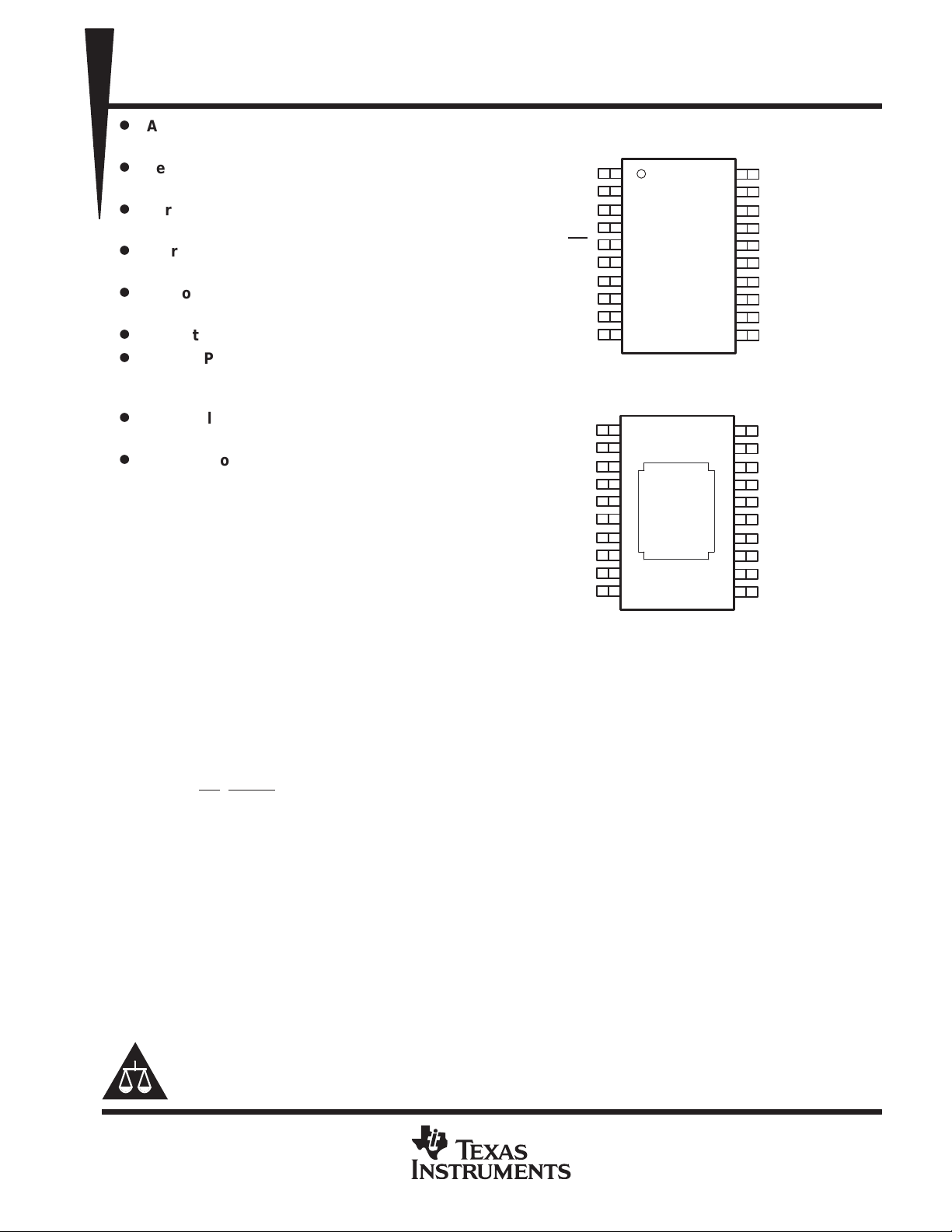
GND/HEATSINK
GND/HEATSINK
GND
NC
EN
IN
IN
NC
GND/HEATSINK
GND/HEATSINK
PWP PACKAGE
(TOP VIEW)
1
2
3
4
5
6
7
8
9
10
PWP PACKAGE
(BOTTOM VIEW)
20
19
18
17
16
15
14
13
12
11
GND/HEATSINK
GND/HEATSINK
NC
NC
PG
SENSE†/FB
OUT
OUT
GND/HEATSINK
GND/HEATSINK
Package
D
Power-Good (PG) Status Output
description
The TPS71Hxx integrated circuits are a family of
Thermal
Pad
micropower low-dropout (LDO) voltage regulators. An order of magnitude reduction in dropout
voltage and quiescent current over conventional
LDO performance is achieved by replacing the
typical pnp pass transistor with a PMOS device.
Because the PMOS device behaves as a
low-value resistor, the dropout voltage is very low
(maximum of 32 mV at an output current of
NC – No internal connection
†
SENSE – Fixed voltage options only (TPS71H33,
TPS71H48, and TPS71H50)
‡
FB – Adjustable version only (TPS71H01)
100 mA for the TPS71H50) and is directly
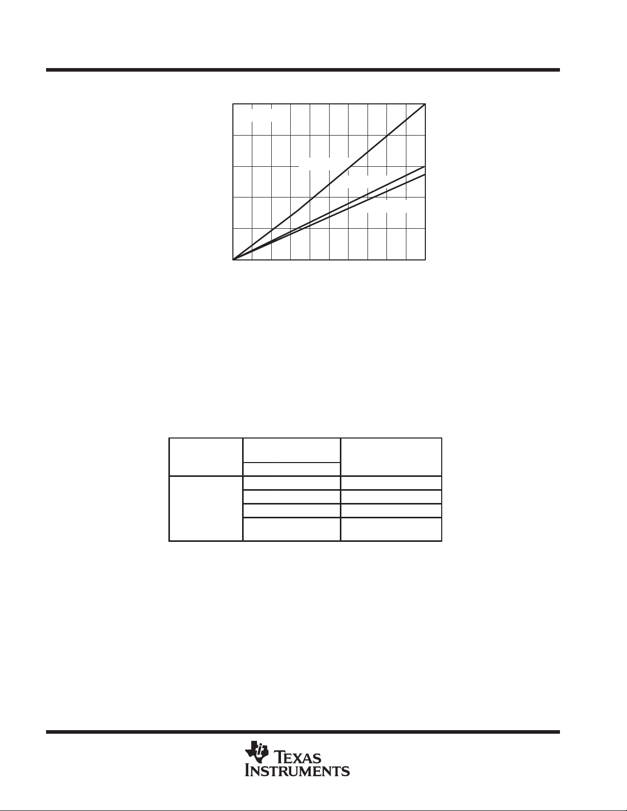
proportional to the output current (see Figure 1). Additionally, since the PMOS pass element is a voltage-driven
device, the quiescent current is very low and remains independent of output loading (typically 285 µA over the
full range of output current, 0 mA to 500 mA). These two key specifications yield a significant improvement in
operating life for battery-powered systems. The LDO family also features a sleep mode; applying a TTL high
signal to EN
(enable) shuts down the regulator, reducing the quiescent current to 0.5 µA maximum at TJ = 25°C.
‡
Please be aware that an important notice concerning availability, standard warranty, and use in critical applications of
Texas Instruments semiconductor products and disclaimers thereto appears at the end of this data sheet.
PRODUCTION DATA information is current as of publication date.
Products conform to specifications per the terms of Texas Instruments
standard warranty. Production processing does not necessarily include
testing of all parameters.
POST OFFICE BOX 655303 • DALLAS, TEXAS 75265
Copyright 1997, Texas Instruments Incorporated
1
TPS71H01Q, TPS71H33Q, TPS71H48Q, TPS71H50Q
J
(PWP)
LOW-DROPOUT VOLTAGE REGULATORS
SLVS152A – NOVEMBER 1996 – REVISED JANUAR Y 1997
description (continued)
0.25
TA = 25°C
0.2
0.15
0.1
Dropout Voltage – V
0.05
0
0 0.05 0.1 0.15 0.2 0.25 0.3
TPS71H33
TPS71H48
TPS71H50
0.35 0.4 0.45 0.5
IO – Output Current – A
Figure 1. Dropout Voltage Versus Output Current
Power good (PG) reports low output voltage and can be used to implement a power-on reset or a low-battery
indicator.
The TPS71Hxx is offered in 3.3-V, 4.85-V, and 5-V fixed-voltage versions and in an adjustable version
(programmable over the range of 1.2 V to 9.75 V). Output voltage tolerance is specified as a maximum of 2%
over line, load, and temperature ranges (3% for adjustable version). The TPS71Hxx family is available in a
TSSOP (20-pin) thermally enhanced surface-mount power package. The package has an innovative thermal
pad that, when soldered to the printed-wiring board (PWB), enables the device to dissipate several watts of
power (see Thermal Information section). Maximum height of the package is 1.2 mm.
AVAILABLE OPTIONS
OUTPUT VOLTAGE
T
–55°C to 150°C
†
The PWP package is only available left-end taped and reeled, as indicated
by the LE suffix on the device type. The TPS71H01Q is programmable using
an external resistor divider (see application information).
(V)
MIN TYP MAX
4.9 5 5.1 TPS71H50QPWPLE
4.75 4.85 4.95 TPS71H48QPWPLE
3.23 3.3 3.37 TPS71H33QPWPLE
Adjustable
1.2 V to 9.75 V
†
TSSOP
TPS71H01QPWPLE
2
POST OFFICE BOX 655303 • DALLAS, TEXAS 75265
TPS71H01Q, TPS71H33Q, TPS71H48Q, TPS71H50Q
LOW-DROPOUT VOLTAGE REGULATORS
SLVS152A – NOVEMBER 1996 – REVISED JANUAR Y 1997
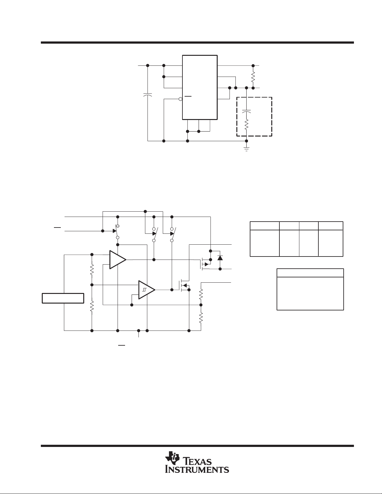
TPS71Hxx
†
functional block diagram
IN
EN
V
ref
= 1.178 V
†
_
+
10
8
IN
9
IN
SENSE
IN
6
EN
GND
V
I
0.1 µF
†
TPS71H33, TPS71H48, TPS71H50 (fixed-voltage options)
‡
Capacitor selection is nontrivial. See application information section
for details.
PG
OUT
OUT
20
15
14
13
+
10 µF
321
CSR
Figure 2. Typical Application Configuration
DEVICE
TPS71H01
TPS71H33
TPS71H48
TPS71H50
NOTE A: Resistors are nominal values only.
1.12 V
††
+
_
PG
OUT
SENSE‡/FB
R1
PG
V
O
‡
C
O
RESISTOR DIVIDER OPTIONS
∞
0
420
726
756
COMPONENT COUNT
MOS transistors
Bilpolar transistors
Diodes
Capacitors
Resistors
233
233
233
UNITR1 R2
Ω
kΩ
kΩ
kΩ
464
41
4
17
76
R2
†
Switch positions are shown with EN
‡
For most applications, SENSE should be externally connected to OUT as close as possible to the device. (For other implementations, refer
to SENSE-pin connection discussion in Applications Information section.)
GND
low (active).
POST OFFICE BOX 655303 • DALLAS, TEXAS 75265
3
TPS71H01Q, TPS71H33Q, TPS71H48Q, TPS71H50Q
PACKAGE
A
PACKAGE
C
LOW-DROPOUT VOLTAGE REGULATORS
SLVS152A – NOVEMBER 1996 – REVISED JANUAR Y 1997
absolute maximum ratings over operating free-air temperature range (unless otherwise noted)
‡
Input voltage range
Output current, I
Continuous total power dissipation See Dissipation Rating Tables 1 and 2. . . . . . . . . . . . . . . . . . . . . . . . . . . . .
Operating virtual junction temperature range, T
Storage temperature range, T
Lead temperature 1,6 mm (1/16 inch) from case for 10 seconds 260°C. . . . . . . . . . . . . . . . . . . . . . . . . . . . . . .
†
Stresses beyond those listed under “absolute maximum ratings” may cause permanent damage to the device. These are stress ratings only, and
functional operation of the device at these or any other conditions beyond those indicated under “recommended operating conditions” is not
implied. Exposure to absolute-maximum-rated conditions for extended periods may affect device reliability.
‡
All voltage values are with respect to network terminal ground.
§
Dissipation rating tables and figures are provided for maintenance of junction temperature at or below
absolute maximum temperature of 150°C. For guidelines on maintaining junction temperature within
recommended operating range, see the Thermal Information section.
¶
Refer to Thermal Information section for detailed power dissipation considerations when using the
TSSOP packages.
, VI, PG, SENSE, EN –0.3 V to 11 V. . . . . . . . . . . . . . . . . . . . . . . . . . . . . . . . . . . . . . . . . . . .
2 A. . . . . . . . . . . . . . . . . . . . . . . . . . . . . . . . . . . . . . . . . . . . . . . . . . . . . . . . . . . . . . . . . . . . . . . . . . .
O
–55°C to 150°C. . . . . . . . . . . . . . . . . . . . . . . . . . . . . . . . . . . . .
–65°C to 150°C. . . . . . . . . . . . . . . . . . . . . . . . . . . . . . . . . . . . . . . . . . . . . . . . . . .
stg
DISSIPATION RA TING TABLE 1 – FREE-AIR TEMPERATURE (see Figure 3)
T
≤ 25°C DERATING FACTOR T
POWER RATING ABOVE TA = 25°CAPOWER RATINGAPOWER RATING
¶
PWP
DISSIPATION RA TING TABLE 2 – CASE TEMPERATURE (see Figure 4)
¶
PWP
700 mW 5.6 mW/°C 448 mW 140 mW
T
≤ 62.5°C DERATING FACTOR T
POWER RATING ABOVE TC = 62.5°CCPOWER RATINGCPOWER RATING
25 W 285.7 mW/°C 22.9 W 7.1 W
J
§
= 70°C T
= 70°C T
= 125°C
§
= 125°C
†
4
POST OFFICE BOX 655303 • DALLAS, TEXAS 75265
TPS71H01Q, TPS71H33Q, TPS71H48Q, TPS71H50Q
LOW-DROPOUT VOLTAGE REGULATORS
SLVS152A – NOVEMBER 1996 – REVISED JANUAR Y 1997
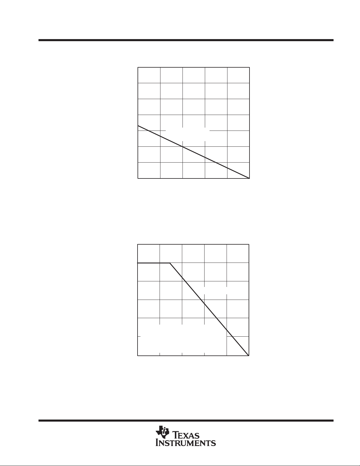
DISSIPATION DERATING CURVE
vs
FREE-AIR TEMPERATURE
1400
1200
1000
800
600
400
200
– Maximum Continuous Dissipation – mW
D
P
0
25 50 75 100
PWP Package
R
= 178°C/W
θJA
TA – Free-Air Temperature – ° C
Figure 3
†
125 150
MAXIMUM CONTINUOUS DISSIPATION
†
vs
CASE TEMPERATURE
30
25
20
PWP Package
15
10
Measured with the exposed thermal pad
coupled to an infinite heat sink with a
5
– Maximum Continuous Dissipation – W
D
P
thermally conductive compound (the
thermal conductivity of the compound
is 0.815 W/m ⋅°C). The R
0
25 50 75 100
TC – Case Temperature – °C
θJC
is 3.5°C/W.
125 150
Figure 4
†
Dissipation rating tables and figures are provided for maintenance of junction temperature at or below absolute maximum temperature of 150°C.
For guidelines on maintaining junction temperature within recommended operating range, see the Thermal Information section.
POST OFFICE BOX 655303 • DALLAS, TEXAS 75265
5
TPS71H01Q, TPS71H33Q, TPS71H48Q, TPS71H50Q
Input voltage, V
†
V
§
J
,
,
Ground current (active mode)
EN ≤ 0.5 V, V
I
V
O
V,
A
Input current (standby mode)
EN
V
2.7 V ≤ V
≤ 10 V
A
Output current limit
V
V
V
A
gy
EN
V
2.7 V ≤ V
V
A
PG leak
t
Normal operation
V
10 V
A
EN logic high (standb
)
40°C to 125°C
V
EN logic l
)
2.7 V ≤ V
V
V
EN i
t
0 V ≤ V
V
A
Minimum V
for active pass element
V
Minimum V
for valid PG
I
300 µA
I
300 µA
V
LOW-DROPOUT VOLTAGE REGULATORS
SLVS152A – NOVEMBER 1996 – REVISED JANUAR Y 1997
recommended operating conditions
MIN MAX UNIT
TPS71H01Q 2.5 10
p
High-level input voltage at EN, V
Low-level input voltage at EN, V
Output current range, I
Operating virtual junction temperature range, T
†
Minimum input voltage defined in the recommended operating conditions is the maximum specified output voltage plus dropout voltage at the
maximum specified load range. Since dropout voltage is a function of output current, the usable range can be extended for lighter loads. To
calculate the minimum input voltage for your maximum output current, use the following equation: V
Because the TPS71H01 is programmable, r
calculating VDO from r
the recommended input voltage range for the TPS71H01.
I
IH
IL
O
is given in Note 2 in the electrical characteristics table. The minimum value of 2.5 V is the absolute lower limit for
DS(on)
DS(on)
electrical characteristics at IO = 10 mA, EN = 0 V , CO = 4.7 µF/CSR‡ = 1 Ω, SENSE/FB shorted to OUT
(unless otherwise noted)
PARAMETER
EN ≤ 0.5 V
0 mA ≤ IO ≤ 500 mA
p
p
Pass-element leakage current in standby
mode
age curren
Output voltage temperature coefficient –40°C to 125°C 61 75 ppm/°C
Thermal shutdown junction temperature 165 °C
y mode
ow (active mode
EN hysteresis voltage 25°C 50 mV
nput curren
I
I
‡
CSR (compensation series resistance) refers to the total series resistance, including the equivalent series resistance (ESR) of the capacitor, any
series resistance added externally, and PWB trace resistance to CO.
§
Pulse-testing techniques are used to maintain virtual junction temperature as close as possible to ambient temperature; thermal effects must
be taken into account separately.
p
O
2.5 V ≤ VI ≤ 6 V
6 V ≤ VI ≤ 10 V
PG
TPS71H33Q 3.77 10
TPS71H48Q 5.2 10
TPS71H50Q 5.33 10
2 V
0.5 V
0 500 mA
J
= V
should be used to calculate VDO before applying the above equation. The equation for
TEST CONDITIONS
=
,
I
= 0,
=
,
I
p
≤ 10
I
≤ 10
I
=
V
= V
+ 1 V
+ 1
I
= 10
I
≤ 10
I
,
=
PG
=
PG
T
25°C 285 350
–40°C to 125°C 460
25°C 0.5
–40°C to 125°C 2
25°C 1.2 2
–40°C to 125°C 2
25°C 0.5
–40°C to 125°C 1
25°C 0.02 0.5
–40°C to 125°C 0.5
°
–
25°C 0.5
–40°C to 125°C 0.5
25°C –0.5 0.5
–40°C to 125°C –0.5 0.5
25°C 2.05 2.5
–40°C to 125°C 2.5
25°C 1.06 1.5
–40°C to 125°C 1.9
I(min)
TPS71H01Q, TPS71H33Q
TPS71H48Q, TPS71H50Q
MIN TYP MAX
°
2
2.7
–40 125 °C
+ V
O(max)
DO(max load)
UNIT
µ
µ
µ
µ
µ
6
POST OFFICE BOX 655303 • DALLAS, TEXAS 75265
PARAMETER
TEST CONDITIONS
‡
T
UNIT
Reference voltage (measured at
V
50 µA ≤ I
150 mA
V
150 mA ≤ I
500 mA
Ω
V
2.9 V
50 µA ≤ I
≤ 500 mA
Input regulation
I
,
µ
O
,
mV
O
,
I
,
mV
Output regulation
O
µ ,
I
,
mV
I
A
Ripple rejection
f
120 H
dB
O
,
†
CSR
†
Ω
PG
§
I
400 µA
V
V
V
FB input current
nA
TPS71H01Q, TPS71H33Q, TPS71H48Q, TPS71H50Q
LOW-DROPOUT VOLTAGE REGULATORS
SLVS152A – NOVEMBER 1996 – REVISED JANUAR Y 1997
TPS71H01 electrical characteristics at IO = 10 mA, V
= 3.5 V, EN = 0 V, CO = 4.7 µF/CSR† = 1 Ω, FB
I
shorted to OUT at device leads (unless otherwise noted)
J
VI = 3.5 V, IO = 10 mA 25°C 1.178 V
FB with OUT connected to FB)
Reference voltage temperature
coefficient
Pass-element series resistance
(see Note 2)
p
p
pp
Output noise-spectral density f = 120 Hz 25°C 2
Output noise voltage
PG trip-threshold voltage
PG hysteresis voltage
p
output low voltage
p
†
CSR refers to the total series resistance, including the ESR of the capacitor, any series resistance added externally, and PWB trace resistance
to CO.
‡
Pulse-testing techniques are used to maintain virtual junction temperature as close as possible to ambient temperature; thermal effects must
be taken into account separately.
§
Output voltage programmed to 2.5 V with closed-loop configuration (see application information).
NOTES: 1. When VI < 2.9 V and IO > 150 mA simultaneously, pass element r
dropout voltage prevents the regulator from maintaining the specified tolerance range.
2. To calculate dropout voltage, use equation:
r
DS(on)
5.9 V , which corresponds to dropout conditions for programmed output voltages of 2.5 V, 3 V, 4 V, and 6 V, respectively. (For other
programmed values, see Figure 26.)
§
§
VDO = IO
⋅ r
is a function of both output current and input voltage. The parametric table lists r
2.5 V ≤ VI ≤ 10 V,
See Note 1
= 2.4 V,
I
= 2.4 V,
I
,
=
I
VI = 3.9 V, 50 µA ≤ IO ≤ 500 mA 25°C 0.32
VI = 5.9 V, 50 µA ≤ IO ≤ 500 mA 25°C 0.23
V
= 2.5 V to 10 V, 50 µA ≤ I
See Note 1
I
= 5 mA to 500 mA, 2.5 V ≤ V
See Note 1
I
= 50 µA to 500 mA, 2.5 V ≤ V
See Note 1
=
10 Hz ≤ f ≤ 100 kHz,
VFB voltage decreasing from above V
Measured at V
PG
DS(on)
=
z
= 1
FB
,
5 mA ≤ IO ≤ 500 mA,
≤
O
≤
O
O
≤ 500 mA,
≤ 10 V,
≤ 10 V,
= 50 µ
O
I
= 500 mA,
See Note 1
CO = 4.7 µF 25°C 95
CO = 10 µF 25°C 89
CO = 100 µF 25°C 74
PG
= 2.13
I
DS(on)
–40°C to 125°C 1.143 1.213 V
–40°C to 125°C 61 75 ppm/°C
25°C 0.7 1
–40°C to 125°C 1
25°C 0.83 1.3
–40°C to 125°C 1.3
25°C 0.52 0.85
–40°C to 125°C 0.85
25°C 18
–40°C to 125°C 25
25°C 14
–40°C to 125°C 25
25°C 22
–40°C to 125°C 54
25°C 48 59
–40°C to 125°C 44
25°C 45 54
–40°C to 125°C 44
–40°C to 125°C 1.101 1.145 V
25°C 12 mV
25°C 0.1 0.4
–40°C to 125°C 0.4
25°C –10 0.1 10
–40°C to 125°C –20 20
increases (see Figure 27) to a point such that the resulting
DS(on)
TPS71H01Q
MIN TYP MAX
µV/√Hz
µVrms
for VI = 2.4 V, 2.9 V, 3.9 V, and
POST OFFICE BOX 655303 • DALLAS, TEXAS 75265
7
TPS71H01Q, TPS71H33Q, TPS71H48Q, TPS71H50Q
PARAMETER
TEST CONDITIONS
‡
T
UNIT
Output voltage
V
I
V
V
D
I
100 mA
V
V
mV
I
500 mA
V
3.23 V
(
O)O
,
I
,
Ω
Input regulation
V
50 µA ≤ I
500 mA
mV
I
5 mA to 500 mA
V
≤ 10 V
mV
Output regulation
I
500 mA
V
V
mV
I
A
Ripple rejection
f
120 H
dB
I
500 mA
CSR
†
Ω
PG output low voltage
I
V
V
V
LOW-DROPOUT VOLTAGE REGULATORS
SLVS152A – NOVEMBER 1996 – REVISED JANUAR Y 1997
TPS71H33 electrical characteristics at IO = 10 mA, V
= 4.3 V , EN = 0 V , CO = 4.7 µF/CSR† = 1 Ω, SENSE
I
shorted to OUT (unless otherwise noted)
J
p
ropout voltage
Pass-element series (3.23 V – V
resistance
p
p
pp
Output noise-spectral density f = 120 Hz 25°C 2
Output noise voltage
PG trip-threshold voltage
PG hysteresis voltage
p
†
CSR refers to the total series resistance, including the ESR of the capacitor, any series resistance added externally, and PWB trace resistance
to CO.
‡
Pulse-testing techniques are used to maintain virtual junction temperature as close as possible to ambient temperature; thermal effects must
be taken into account separately.
VI = 4.3 V, IO = 10 mA 25°C 3.3
4.3 V ≤ VI ≤ 10 V, 5 mA ≤ IO ≤ 500 mA –40°C to 125°C 3.23 3.37
= 10 mA,
O
=
O
=
O
IO = 500 mA
= 4.3 V to 10 V,
I
=
O
= 50 µA to
O
=
10 Hz ≤ f ≤ 100 kHz,
VO voltage decreasing from above V
= 1 mA,
PG
†
= 1
=
,
,
)/I
, V
z
= 3.23
I
= 3.23
I
=
I
= 3.23 V,
,4.3 V ≤
,4.3 V ≤
= 50 µ
O
=
O
CO = 4.7 µF
CO = 10 µF
CO = 100 µF
= 2.8
I
O
I
I
≤
≤ 10
PG
25°C 4.5 7
–40°C to 125°C 8
25°C 47 60
–40°C to 125°C 80
25°C 235 300
–40°C to 125°C 400
25°C 0.47 0.6
–40°C to 125°C 0.8
25°C 20
–40°C to 125°C 27
25°C 21 38
–40°C to 125°C 75
25°C 30 60
–40°C to 125°C 120
25°C 43 54
–40°C to 125°C 40
25°C 39 49
–40°C to 125°C 36
25°C 274
25°C 228
25°C 159
–40°C to 125°C 2.868 3 V
25°C 35 mV
25°C 0.22 0.4
–40°C to 125°C 0.4
TPS71H33Q
MIN TYP MAX
µV/√Hz
µVrms
8
POST OFFICE BOX 655303 • DALLAS, TEXAS 75265
PARAMETER
TEST CONDITIONS
‡
T
UNIT
Output voltage
V
I
V
V
D
I
100 mA
V
V
mV
I
500 mA
V
V
(
O)O
,
I
,
Ω
Input regulation
V
50 µA ≤ I
500 mA
mV
I
500 mA
V
V
mV
Output regulation
I
50 µA to 500 mA
V
≤ 10 V
mV
I
A
Ripple rejection
f
120 H
dB
I
500 mA
CSR
†
Ω
PG
I
V
V
V
TPS71H01Q, TPS71H33Q, TPS71H48Q, TPS71H50Q
LOW-DROPOUT VOLTAGE REGULATORS
SLVS152A – NOVEMBER 1996 – REVISED JANUAR Y 1997
TPS71H48 electrical characteristics at IO = 10 mA, V
= 5.85 V, EN = 0 V, CO = 4.7 µF/CSR† = 1 Ω,
I
SENSE shorted to OUT (unless otherwise noted)
J
p
ropout voltage
Pass-element series (4.75 V – V
resistance
p
p
pp
Output noise-spectral density f = 120 Hz 25°C 2 µV/√Hz
Output noise voltage
PG trip-threshold voltage
PG hysteresis voltage
output low voltage
†
CSR refers to the total series resistance, including the ESR of the capacitor, any series resistance added externally, and PWB trace resistance
to CO.
‡
Pulse-testing techniques are used to maintain virtual junction temperature as close as possible to ambient temperature; thermal effects must
be taken into account separately.
VI = 5.85 V, IO = 10 mA 25°C 4.85
5.85 V ≤ VI ≤ 10 V, 5 mA ≤ IO ≤ 500 mA –40°C to 125°C 4.75 4.95
= 10 mA,
O
=
O
=
O
IO = 500 mA
= 5.85 V to 10 V,
I
= 5 mA to
O
=
O
=
10 Hz ≤ f ≤ 100 kHz,
VO voltage decreasing from above V
= 1.2 mA,
PG
†
= 1
=
,
,
)/I
, V
z
= 4.75
I
= 4.75
I
= 4.75
I
= 4.75 V,
,5.85 V ≤
,5.85 V ≤
= 50 µ
O
=
O
CO = 4.7 µF
CO = 10 µF
CO = 100 µF
= 4.12
I
O
≤
≤ 10
I
I
PG
25°C 2.9 6
–40°C to 125°C 8
25°C 30 37
–40°C to 125°C 54
25°C 150 180
–40°C to 125°C 250
25°C 0.32 0.35
–40°C to 125°C 0.52
25°C 27
–40°C to 125°C 37
25°C 12 42
–40°C to 125°C 80
25°C 42 60
–40°C to 125°C 130
25°C 42 53
–40°C to 125°C 39
25°C 39 50
–40°C to 125°C 35
25°C 410
25°C 328
25°C 212
–40°C to 125°C 4.5 4.7 V
25°C 50 mV
25°C 0.2 0.4
–40°C to 125°C 0.4
TPS71H48Q
MIN TYP MAX
µVrms
POST OFFICE BOX 655303 • DALLAS, TEXAS 75265
9
TPS71H01Q, TPS71H33Q, TPS71H48Q, TPS71H50Q
PARAMETER
TEST CONDITIONS
‡
T
UNIT
Output voltage
V
I
V
V
D
I
100 mA
V
V
mV
I
500 mA
V
V
(
O)O
,
I
Ω
Input regulation
V
50 µA ≤ I
500 mA
mV
I
500 mA
V
V
mV
Output regulation
I
50 µA to 500 mA
V
≤ 10 V
mV
I
A
Ripple rejection
f
120 H
dB
I
500 mA
CSR
†
Ω
PG output low voltage
I
V
V
V
LOW-DROPOUT VOLTAGE REGULATORS
SLVS152A – NOVEMBER 1996 – REVISED JANUAR Y 1997
TPS71H50 electrical characteristics at IO = 10 mA, V
= 6 V , EN = 0 V , CO = 4.7 µF/CSR† = 1 Ω, SENSE
I
shorted to OUT (unless otherwise noted)
J
p
ropout voltage
Pass-element series (4.88 V – V
resistance
p
p
pp
Output noise-spectral density f = 120 Hz 25°C 2
Output noise voltage
PG trip-threshold voltage
PG hysteresis voltage
p
†
CSR refers to the total series resistance, including the ESR of the capacitor, any series resistance added externally, and PWB trace resistance
to CO.
‡
Pulse-testing techniques are used to maintain virtual junction temperature as close as possible to ambient temperature; thermal effects must
be taken into account separately.
VI = 6 V, IO = 10 mA 25°C 5
6 V ≤ VI ≤ 10 V, 5 mA ≤ IO ≤ 500 mA –40°C to 125°C 4.9 5.1
= 10 mA,
O
=
O
=
O
IO = 500 mA
= 6 V to 10 V,
I
= 5 mA to
O
=
O
=
10 Hz ≤ f ≤ 100 kHz,
VO voltage decreasing from above V
= 1.2 mA,
PG
†
= 1
=
,
,
)/I
, V
z
= 4.88
I
= 4.88
I
= 4.88
I
= 4.88 V.
,6 V ≤
,6 V ≤
= 50 µ
O
=
O
CO = 4.7 µF
CO = 10 µF
CO = 100 µF
= 4.25
I
O
≤ 10
I
I
≤
PG
25°C 2.9 6
–40°C to 125°C 8
25°C 27 32
–40°C to 125°C 47
25°C 146 170
–40°C to 125°C 230
25°C 0.29 0.32
–40°C to 125°C 0.47
25°C 25
–40°C to 125°C 32
25°C 30 45
–40°C to 125°C 86
25°C 45 65
–40°C to 125°C 140
25°C 45 55
–40°C to 125°C 40
25°C 42 52
–40°C to 125°C 36
25°C 430
25°C 345
25°C 220
–40°C to 125°C 4.55 4.75 V
25°C 53 mV
25°C 0.2 0.4
–40°C to 125°C 0.4
TPS71H50Q
MIN TYP MAX
µV/√Hz
µVrms
10
POST OFFICE BOX 655303 • DALLAS, TEXAS 75265

VOOutput voltage
rrent
Ripple rejection
Frequenc
Output spectral noise densit
s
Freq
enc
V
CSR
Compensation series resistance
rrent
CSR
Compensation series resistance
Ceramic capacitance
CSR
Compensation series resistance
rrent
CSR
Compensation series resistance
Ceramic capacitance
TPS71H01Q, TPS71H33Q, TPS71H48Q, TPS71H50Q
LOW-DROPOUT VOLTAGE REGULATORS
SLVS152A – NOVEMBER 1996 – REVISED JANUAR Y 1997
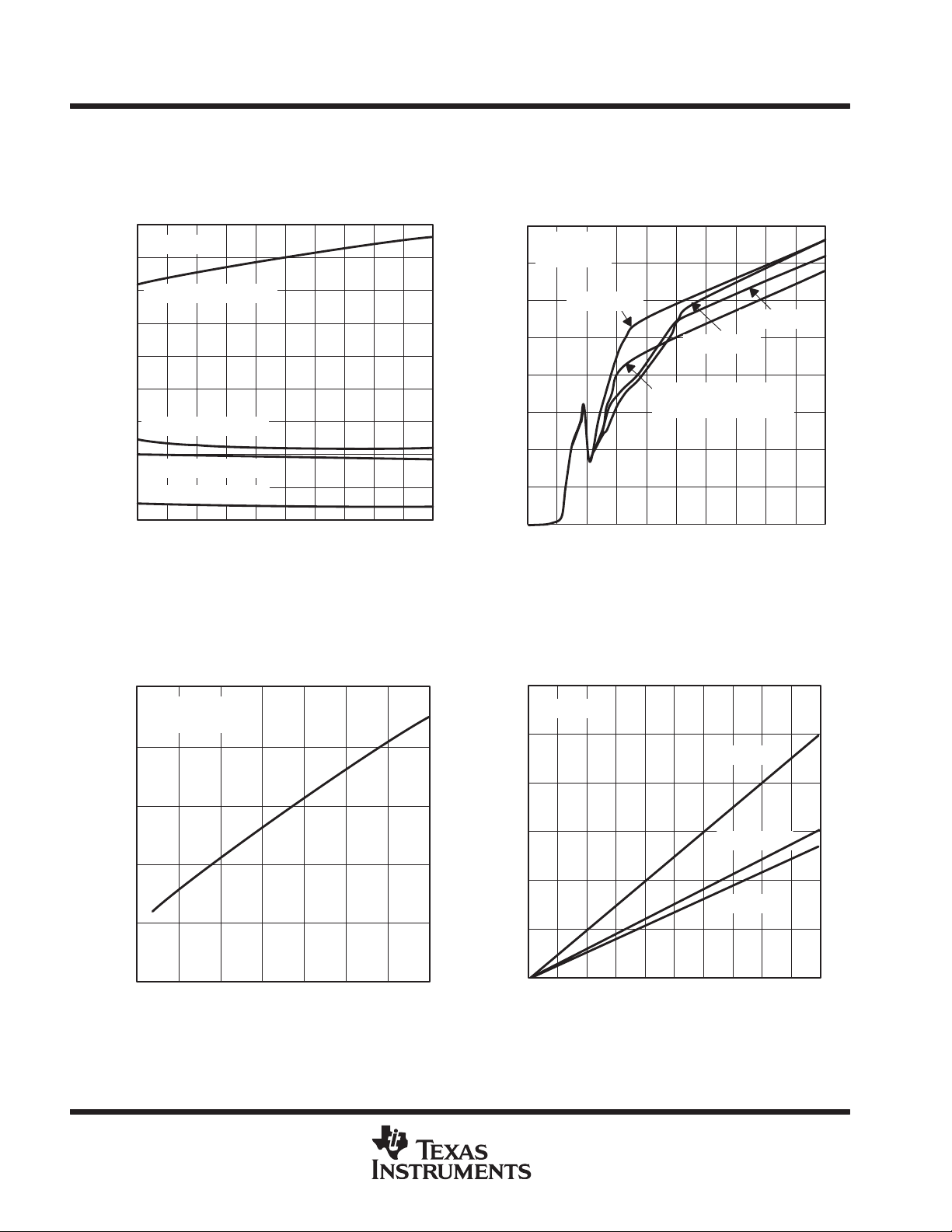
TYPICAL CHARACTERISTICS
Table of Graphs
FIGURE
vs Output current 5
I
Q
V
DO
∆V
DO
∆V
O
V
O
∆V
O
r
DS(on)
R Divider resistance vs Free-air temperature 26
I
I(SENSE)
I
I
I(EN)
V
PG
Quiescent current
Typical dropout voltage vs Output current 8
Change in dropout voltage vs Free-air temperature 9
Change in output voltage vs Free-air temperature 10
Output voltage vs Input voltage 11
Change in output voltage vs Input voltage 12
p
pp
p
p
Pass-element resistance vs Input voltage 25
SENSE current vs Free-air temperature 27
FB leakage current vs Free-air temperature 28
Minimum input voltage for active-pass element vs Free-air temperature 29
Minimum input voltage for valid PG vs Free-air temperature 30
Input current (EN) vs Free-air temperature 31
Output voltage response from Enable (EN) 32
Power-good (PG) voltage vs Output voltage 33
p
p
p
p
yv
vs Input voltage 6
vs Free-air temperature 7
13
p
vs Output cu
vs
vs Output cu
vs
vs Output cu
vs
y
u
y
p
p
p
p
14
15
16
17
18
19
20
21
22
23
24
34
35
36
37
38
39
40
41
POST OFFICE BOX 655303 • DALLAS, TEXAS 75265
11
TPS71H01Q, TPS71H33Q, TPS71H48Q, TPS71H50Q
LOW-DROPOUT VOLTAGE REGULATORS
SLVS152A – NOVEMBER 1996 – REVISED JANUAR Y 1997
TYPICAL CHARACTERISTICS
355
TA = 25°C
345
335
Aµ
– Quiescent Current –
Q
I
TPS71Hxx, VI = 10 V
325
315
305
295
TPS71H50, VI = 6 V
285
TPS71H48, VI = 5.85 V
275
TPS71H33, VI = 4.3 V
265
0 50 100 150 200 250 300
FREE-AIR TEMPERATURE
400
VI = V
O(nom)
IO = 10 mA
350
Aµ
300
250
– Quiesent Current –
Q
I
200
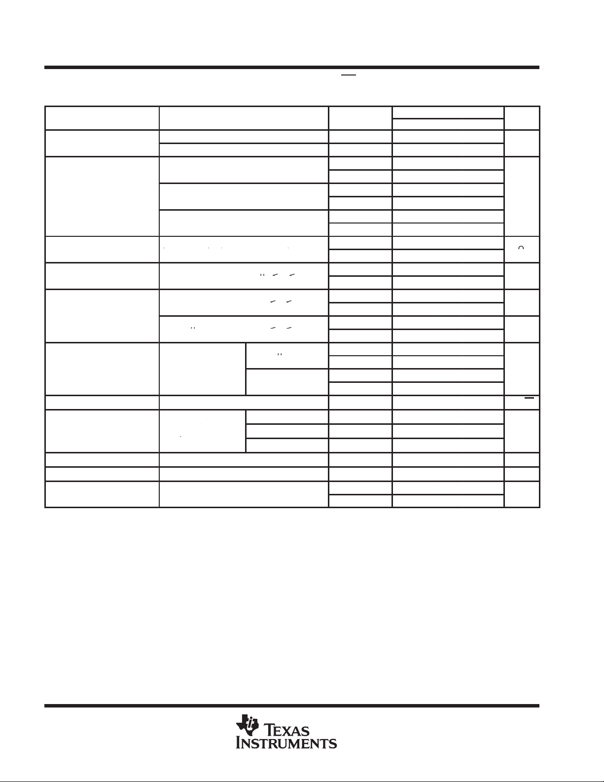
QUIESCENT CURRENT
vs
OUTPUT CURRENT
350 400 450 500
IO – Output Current – mA
Figure 5
TPS71H48Q
QUIESCENT CURRENT
vs
+ 1 V
QUIESCENT CURRENT
INPUT VOLTAGE
400
TA = 25°C
RL = 10 Ω
350
Aµ
300
250
200
150
– Quiescent Current –
Q
100
I
50
0
0123456
TPS71H33
VI – Input Voltage – V
Figure 6
DROPOUT VOLTAGE
OUTPUT CURRENT
0.3
TA = 25°C
0.25
0.2
0.15
Dropout Voltage – V
0.1
0.05
vs
TPS71H48
TPS71H50
TPS71H01 With V
Programmed to 2.5 V
O
78910
vs
TPS71H33
TPS71H48
TPS71H50
12
150
–50 –25 0 25 50 75 100 125
TA – Free-Air Temperature – ° C
Figure 7
POST OFFICE BOX 655303 • DALLAS, TEXAS 75265
0
0 50 100 150 200 250 300
IO – Output Current – mA
Figure 8
350 400 450 500
 Loading...