

Page 1

www.ti.com
Table of Contents
User’s Guide
TPS65994 EVM User Guide
ABSTRACT
This document is the user guide for the TPS65994 Evaluation Module. The TPS65994 EVM allows for evaluation
of the TPS65994 IC (WCSP and QFN package) functionality as part of a stand-alone testing kit and for
development and testing of USB Type-C™ and Power Delivery (PD) end products.
Table of Contents
1 About this Manual...................................................................................................................................................................3
2 Items Required for Operation................................................................................................................................................ 3
3 Introduction.............................................................................................................................................................................3
4 Setup........................................................................................................................................................................................4
4.1 Switch, Push Button, Connector, and Test Point Descriptions...........................................................................................4
4.2 LED Indicators Description.................................................................................................................................................9
5 Tiva USB to I2C Bridge Support Integration...................................................................................................................... 10
5.1 Flash Application Firmware to EEPROM......................................................................................................................... 10
5.2 Entering Debug Mode...................................................................................................................................................... 13
6 Using the TPS65994EVM......................................................................................................................................................17
6.1 Powering the TPS65994EVM.......................................................................................................................................... 17
6.2 Firmware Configurations.................................................................................................................................................. 17
7 Connecting the EVM.............................................................................................................................................................18
7.1 Connecting to Various Devices........................................................................................................................................ 18
8 Debugging the EVM..............................................................................................................................................................19
8.1 Connection Not Established.............................................................................................................................................19
8.2 Resetting Behavior...........................................................................................................................................................19
9 TPS65994EVM Schematics.................................................................................................................................................. 20
10 TPS65994EVM Board Layout.............................................................................................................................................27
11 TPS65994EVM Bill of Materials..........................................................................................................................................32
12 TPS65994QFNEVM Schematics........................................................................................................................................ 36
13 TPS65994QFNEVM Board Layout..................................................................................................................................... 44
14 TPS65994QFNEVM Bill of Materials..................................................................................................................................49
15 Revision History................................................................................................................................................................. 53
List of Figures
Figure 4-1. TPS65994 Power Path Jumper Configuration.......................................................................................................... 4
Figure 4-2. ADCIN1 and ADCIN2 Configuration Schematic........................................................................................................5
Figure 4-3. Barrel Jack (J2) Schematic....................................................................................................................................... 5
Figure 4-4. USB Type-C™ Receptacle (J3_PA) Schematic........................................................................................................ 6
Figure 4-5. USB Type-C™ Receptacle (J3_PB) Schematic........................................................................................................6
Figure 4-6. USB Micro-B Receptacle (J6) Schematic..................................................................................................................7
Figure 4-7. Aardvark Connector (J9) Schematic......................................................................................................................... 7
Figure 4-8. Debug Header (J4) Schematic.................................................................................................................................. 8
Figure 4-9. Debug Header (J5) Schematic.................................................................................................................................. 9
Figure 5-1. Application Customization Tool............................................................................................................................... 10
Figure 5-2. I/O Config Register.................................................................................................................................................. 11
Figure 5-3. Flash Project to EEPROM (I2C)..............................................................................................................................12
Figure 5-4. USB to I2C/SPI Adapter Settings............................................................................................................................ 13
Figure 5-5. I2C Addresses.........................................................................................................................................................14
Figure 5-6. Addressing range.................................................................................................................................................... 15
Figure 5-7. Transmit Source Capabilities...................................................................................................................................16
Figure 9-1. TPS65994EVM Block Diagram............................................................................................................................... 20
Figure 9-2. TPS65994EVM PD Controller................................................................................................................................. 21
SLVUBM1C – JANUARY 2019 – REVISED JANUARY 2021
Submit Document Feedback
Copyright © 2021 Texas Instruments Incorporated
TPS65994 EVM User Guide 1
Page 2

Trademarks
Figure 9-3. TPS65994EVM Power Supplies..............................................................................................................................21
Figure 9-4. TPS65994EVM USB Type-C™ Connector.............................................................................................................. 22
Figure 9-5. TPS65994EVM Tiva Debug.................................................................................................................................... 24
Figure 9-6. TPS65994EVM Connectors.................................................................................................................................... 25
Figure 9-7. TPS65994EVM Expansion Connector.................................................................................................................... 26
Figure 10-1. TPS65994EVM Top Silk Screen............................................................................................................................27
Figure 10-2. TPS65994EVM Top Layer.....................................................................................................................................27
Figure 10-3. TPS65994EVM GND Plane 1............................................................................................................................... 28
Figure 10-4. TPS65994EVM High Speed Layer........................................................................................................................28
Figure 10-5. TPS65994EVM GND Plane 2............................................................................................................................... 29
Figure 10-6. TPS65994EVM Power 1 Layer............................................................................................................................. 29
Figure 10-7. TPS65994EVM Power 2 Layer............................................................................................................................. 30
Figure 10-8. TPS65994EVM GND Plane 3............................................................................................................................... 30
Figure 10-9. TPS65994EVM Bottom Layer............................................................................................................................... 31
Figure 10-10. TPS65994EVM Bottom Silk Screen.................................................................................................................... 31
Figure 12-1. TPS65994QFNEVM Block Diagram......................................................................................................................36
Figure 12-2. TPS65994QFNEVM PD Controller....................................................................................................................... 37
Figure 12-3. TPS65994QFNEVM Power Supplies.................................................................................................................... 38
Figure 12-4. TPS65994QFNEVM USB Type-C™ Connector ....................................................................................................39
Figure 12-5. TPS65994QFNEVM Tiva Debug...........................................................................................................................41
Figure 12-6. TPS65994QFNEVM Connectors...........................................................................................................................42
Figure 12-7. TPS65994QFNEVM Expansion Connector...........................................................................................................43
Figure 13-1. TPS65994QFNEVM Top Silk Screen.................................................................................................................... 44
Figure 13-2. TPS65994QFNEVM Top Layer............................................................................................................................. 44
Figure 13-3. TPS65994QFNEVM GND Plane 1........................................................................................................................45
Figure 13-4. TPS65994QFNEVM High Speed Layer................................................................................................................ 45
Figure 13-5. TPS65994QFNEVM GND Plane 2........................................................................................................................46
Figure 13-6. TPS65994QFNEVM Power 1 Layer......................................................................................................................46
Figure 13-7. TPS65994QFNEVM Power 2 Layer......................................................................................................................47
Figure 13-8. TPS65994QFNEVM GND Plane 3........................................................................................................................47
Figure 13-9. TPS65994QFNEVM Bottom Layer........................................................................................................................48
Figure 13-10. TPS65994QFNEVM Bottom Silk Screen............................................................................................................ 48
www.ti.com
List of Tables
Table 4-1. S1 and S2: ADCIN1 and ADCIN2 Switch Settings..................................................................................................... 4
Table 4-2. Port A MUX CTL LED................................................................................................................................................. 9
Table 4-3. Port B MUX CTL LED................................................................................................................................................. 9
Table 11-1. TPS65994EVM BOM.............................................................................................................................................. 32
Table 14-1. TPS65994QFNEVM Bill of Materials...................................................................................................................... 49
Trademarks
USB Type-C™ are trademarks of USB Implementers Forum.
All trademarks are the property of their respective owners.
2 TPS65994 EVM User Guide SLVUBM1C – JANUARY 2019 – REVISED JANUARY 2021
Copyright © 2021 Texas Instruments Incorporated
Submit Document Feedback
Page 3

www.ti.com
About this Manual
1 About this Manual
This user's guide describes the TPS65994 EVM. The guide consists of an introduction, setup instructions, the
EVM schematic, board layouts, component views, internal power (PWR) and ground (GND) plane layouts, and a
bill of materials (BOM). Refer to TPS65994QFNEVM schematic, board layouts, component views when
evaluating TPS65994 QFN package.
2 Items Required for Operation
The following items are required to use the TPS65994 EVM:
• TPS65994 data sheet
• TPS65994 EVM
• TPS65994 Application Customization Tool
• 20-V barrel jack adapter or DC power supply
• Passive USB Type-C™ cables
• USB Type-A to USB Micro-B cable
• USB Type-A to USB Type-B cable
• Mini-DisplayPort to DisplayPort cables
• DP-Expansion Board
• Notebook with USB 2.0, USB 3.0, and DP capabilities
3 Introduction
The TPS65994 is a stand-alone USB Type-C and Power Delivery (PD) controller providing cable plug and
orientation detection at the USB Type-C connector. Upon cable plug and orientation detection, the TPS65994
communicates on the CC line using the USB PD protocol. When cable detection and USB PD negotiation are
complete, the TPS65994 enables the appropriate power path and configures external multiplexers and alternate
mode settings. This user guide describes how the TPS65994 EVM can be used to test DisplayPort alternate
mode as well as USB Data. This guide also contains testing procedures of DP alternate mode as well as various
PD power configurations. The EVM is customizable through the TPS65994 Configuration Tool. Additionally, the
EVM is equipped with Tiva MCU and Aardvark connector to SPI or I2C interfaces for debugging and
development.
SLVUBM1C – JANUARY 2019 – REVISED JANUARY 2021
Submit Document Feedback
Copyright © 2021 Texas Instruments Incorporated
TPS65994 EVM User Guide 3
Page 4
Setup www.ti.com
4 Setup
This section describes the various EVM features and how to test these features. Schematic screen shots,
pictures, and block diagrams are provided as necessary.
4.1 Switch, Push Button, Connector, and Test Point Descriptions
Components described in this section are listed with respect to the EVM from left to right and top to bottom.
Related components are listed simultaneously.
4.1.1 Power Path Jumper Configuration
Out of the box, the TPS65994 EVM has jumper configuration for a TPS65994 device. With this configuration, the
two internal power paths are configured as Source paths for their respective USB Type-C ports. The two external
power paths are configured as Sink paths for their respective USB Type-C ports. When using the TPS65994
EVM, use a TPS65994 template in the TPS65994 Application Customization Tool.
Figure 4-1. TPS65994 Power Path Jumper Configuration
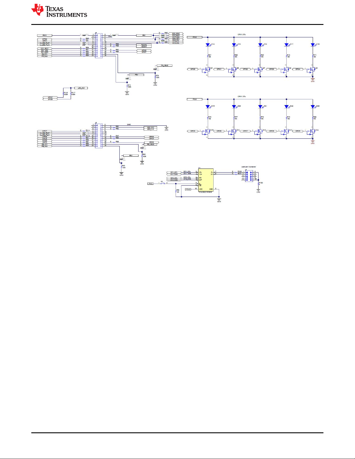
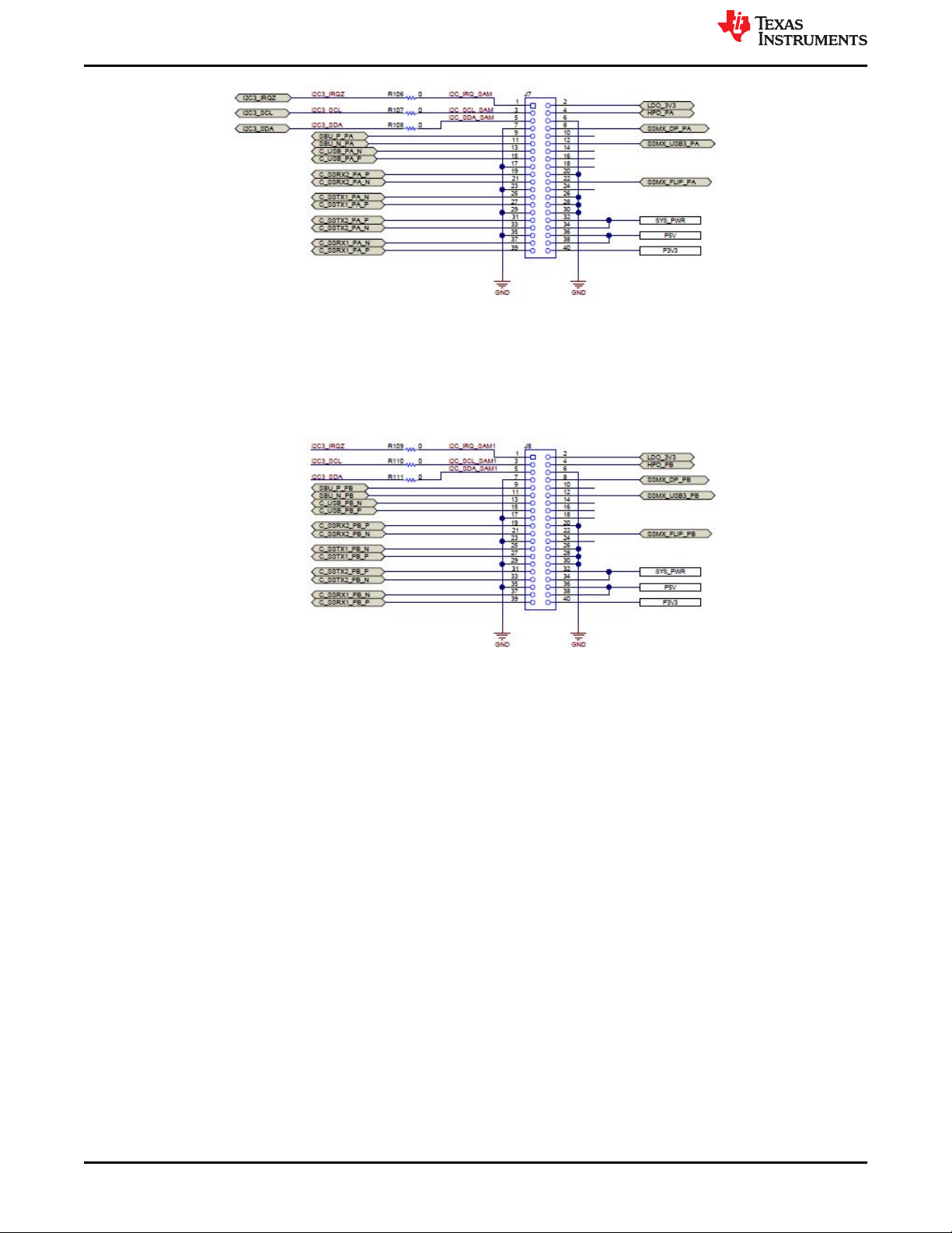
4.1.2 Expansion Ports
J7 and J8 are the connectors for 10G-EXPANSION-EVM Source Board for port A and B respectively. Connect
10G-EXPANSION-EVM Source Board to evaluate DisplayPort and USB 3.2 Data. Both ports can support DP at
the same time.
Note
TPS65994 can only support DP_DFP mode. TPS65994 EVM will work with 10G-EXPANSION-EVM
Source Board only.
4.1.3 ADCINx Settings
4.1.3.1 S1 and S2: ADCIN1 and ADCIN2
The TPS65994 EVM has a switch (S1) that can be used to configure the ADCIN1 and ADCIN2 pin strapping
settings of the TPS65994. ADCIN1 is controlled through S1 and ADCIN2 is controlled through S2. Refer to
TPS65994 datasheet to see different ADCINx configurations. Table 4-1 highlights the switch settings to enable
the different ADCINx configurations. With all switches on S1 and S2 disabled, switches S4A and S4B can be
used to directly short the ADCINx pin to LDO_1V5. The schematic for the ADCIN1 and ADCIN2 configuration
switches can be seen in Figure 4-2.
Table 4-1. S1 and S2: ADCIN1 and ADCIN2 Switch Settings
ADCINx Switch Settings
1 2 3 4 Setting
0 0 0 0 0
0 0 1 1 1
0 1 0 1 2
0 1 1 1 3
0 0 1 0 4
4 TPS65994 EVM User Guide SLVUBM1C – JANUARY 2019 – REVISED JANUARY 2021
Copyright © 2021 Texas Instruments Incorporated
Submit Document Feedback
Page 5
GND
GND
PA_CC1
PA_CC2
PB_ CC1
PB_ CC2
ADCIN2
LDO_3V3
63
1 8
2 7
54
S2
59.0kR22
249kR26
976kR27
GND
All Off Se tting 0
Switch 2 & 4 On S etting 2
Switch 3 & 4 On S etting 1
Switch 2 & 3 & 4 On S etting 3
Switch 3 On Setting 4
Switch 2 On Setting 5
Switch 1 On Setting 6
Switch 1 & 2 On S etting 7
LDO_3V3
ADCIN1
63
1 8
2 7
54
S1
59.0kR12
249kR13
976kR15
GND
LDO_3V3
TP2
TP3
TP4
TP5
2 3
S4B
1 4
S4A
LDO_1V5
LDO_1V5
330pFC1330pF
C2
330pF
C7
330pF
C6
499k
R11
40.2k
R16
499k
R20
40.2k
R28
www.ti.com
0 1 0 0 5
1 0 0 0 6
1 1 0 0 7
Setup
Table 4-1. S1 and S2: ADCIN1 and ADCIN2 Switch Settings (continued)
ADCINx Switch Settings
Figure 4-2. ADCIN1 and ADCIN2 Configuration Schematic
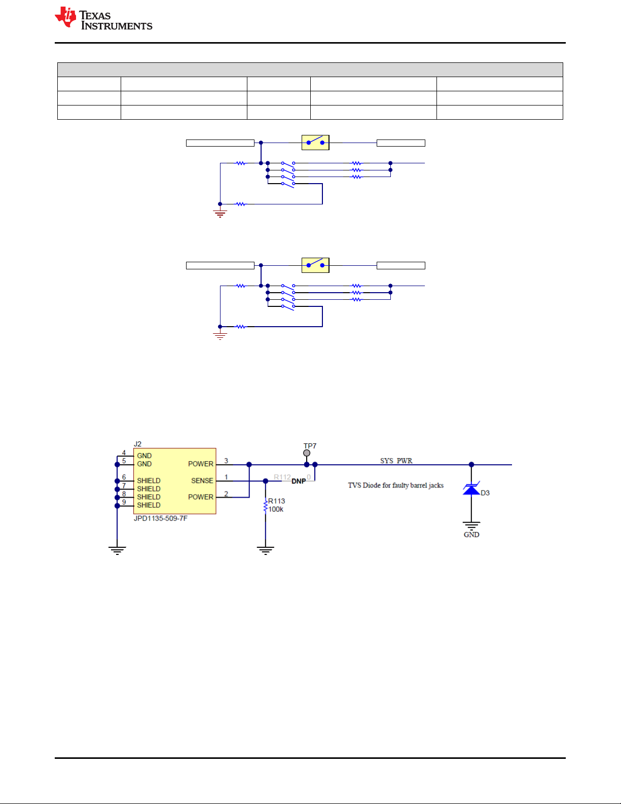
4.1.4 J2: Barrel Jack Power Connector
The barrel jack power connector accepts a 19-V to 20-V DC supply. A standard notebook adapter (or similar
adapter) provides the required power. This input provides the PP_EXT power rail 19-V to 20-V.
Figure 4-3. Barrel Jack (J2) Schematic
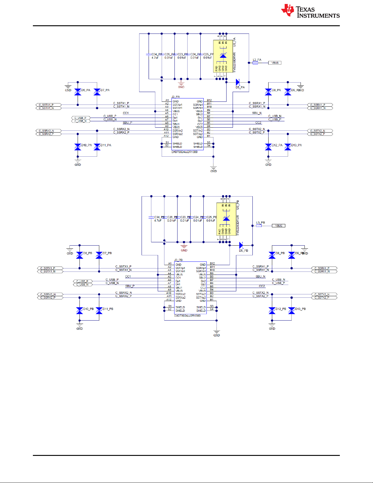
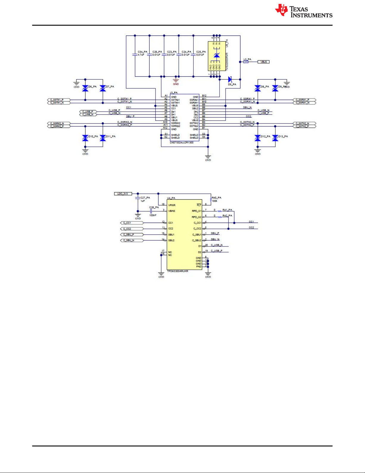
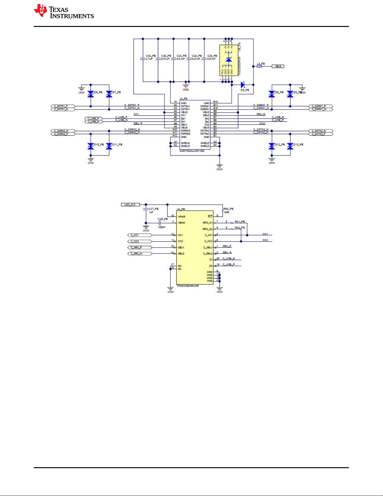
4.1.5 USB Type-C™ Connector (J3_PA, J3_PB)
The TPS65994 EVM has two full feature USB Type-C receptacles (port A/B) and routes VBUS, SSTX and SSRX
pairs, SBU1 and SBU2 pairs, and D+ and D– signals. The TPS65994 device can be used in self-powered and
bus-powered configurations for added flexibility. When self-powered, the EVM can provide up to 15 W (5 V, at 3
A) of power per port via the internal PP5V power path. The EVM is also capable of sinking 100 W (20 V, at 5 A)
of power via the external PP_EXT power path. The internal power path is used for sourcing power and the
external power path is used for sinking power.
SLVUBM1C – JANUARY 2019 – REVISED JANUARY 2021
Submit Document Feedback
Copyright © 2021 Texas Instruments Incorporated
TPS65994 EVM User Guide 5
Page 6
Setup
www.ti.com
Figure 4-4. USB Type-C™ Receptacle (J3_PA) Schematic
Figure 4-5. USB Type-C™ Receptacle (J3_PB) Schematic
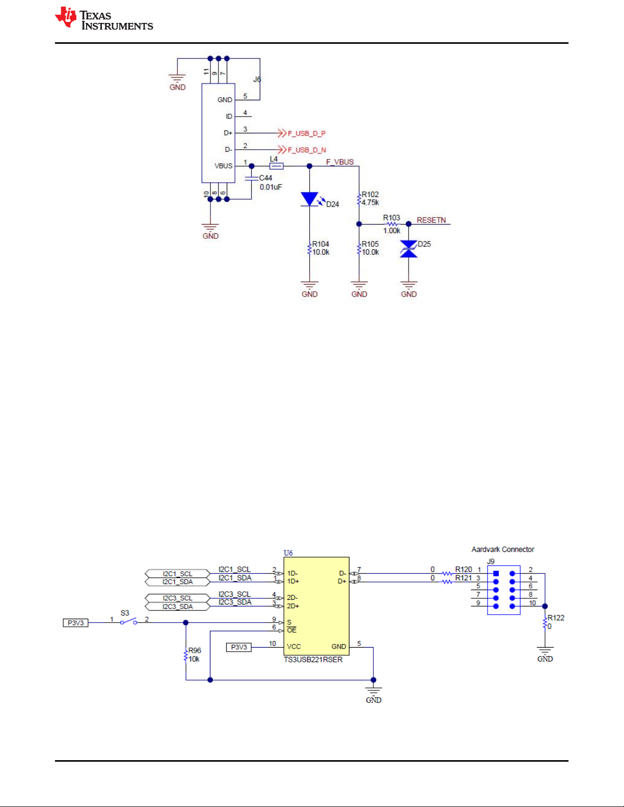
4.1.6 USB Micro B Connector (J6)
J6, the micro-B receptacle connects the Tiva to the PC for the TPS65994 Customization GUI. Use a standard
USB micro-B to Type-A cable to make this connection. LED D24 turns on when VBUS is present on the Tiva
board.
6 TPS65994 EVM User Guide SLVUBM1C – JANUARY 2019 – REVISED JANUARY 2021
Copyright © 2021 Texas Instruments Incorporated
Submit Document Feedback
Page 7
www.ti.com
Setup
Figure 4-6. USB Micro-B Receptacle (J6) Schematic
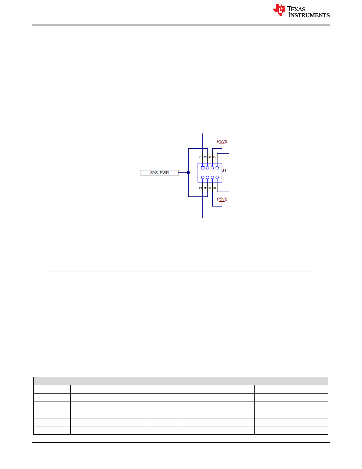
4.1.7 TP8 (5V), J10 (3.3V), TP7 (SYS_PWR)
Use the TP8, and J10 test points to measure the output voltage of the onboard DC/DC converters. These
DC/DC converters produce the required voltage rails for full functionality of the EVM including power delivery,
powering internal and external circuits, and so forth. These test points allow the user to verify the system
supplies on the TPS65994EVM. LDO_1V5 is internally generated for internal circuitry. Use P3V3 to supply
VIN_3V3 which then supplies LDO_3V3. Also, use LDO_3V3 as a low power output for external flash memory.
In bus-powered conditions, or self-powered conditions, LDO_3V3 is active. TP7 test point is provided to verify
input voltage of barrel jack connector.
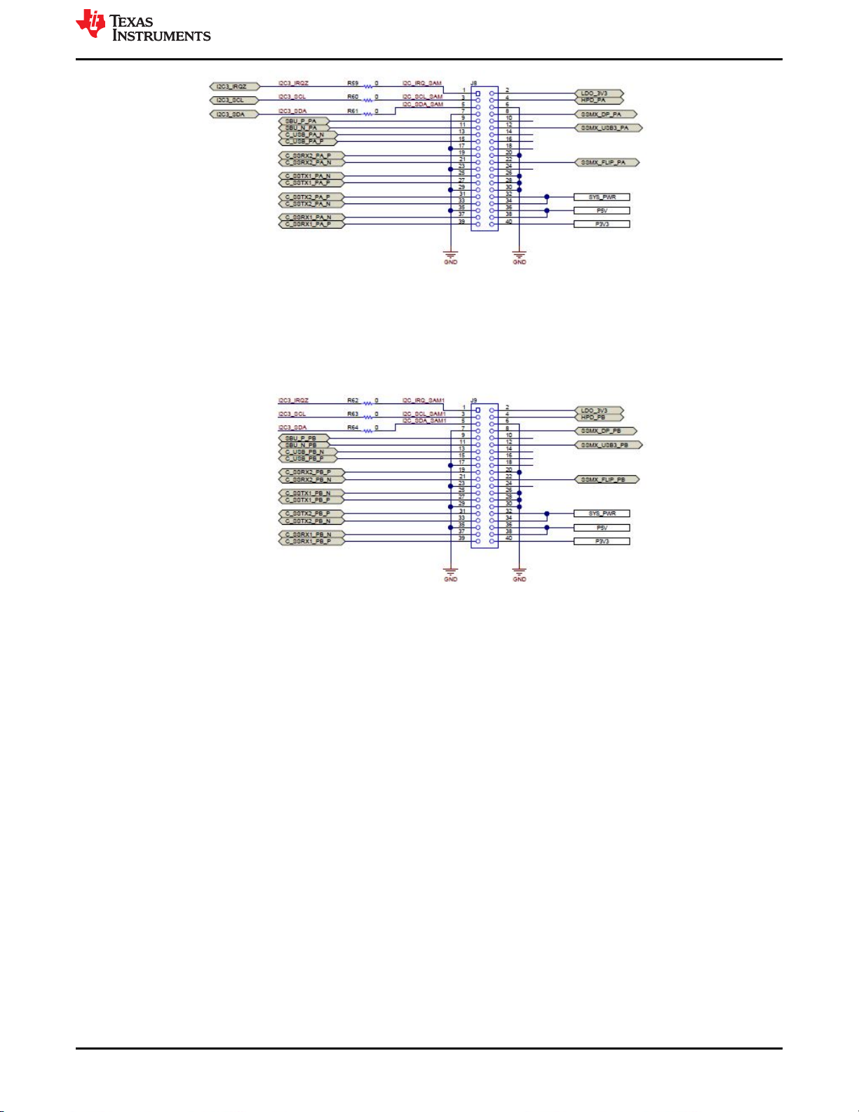
4.1.8 Aardvark Connector (J9)
This connector matches the Total Phase® Aardvark that allows the user to access the I2C pins on the
TPS65994EVM using the I2C Master capabilities. U6 is used to swap between I2C1 or I2C3 connected to the
aardvark connector. S3 is used to control which way the 2 to 1 MUX will be set. If S3 is disabled, by default, I2C1
would be connected to the Aardvark header. When S3 is enabled, I2C3 would be connected to the Aardvark
header.
Figure 4-7. Aardvark Connector (J9) Schematic
SLVUBM1C – JANUARY 2019 – REVISED JANUARY 2021
Submit Document Feedback
Copyright © 2021 Texas Instruments Incorporated
TPS65994 EVM User Guide 7
Page 8
Setup
www.ti.com
4.1.9 TP10, TP11, TP12, TP13: GND Test Points
TP10, TP11, TP12, TP13 GND test points are provided for attaching an oscilloscope or multimeter, as well as for
load testing. These test points are connected to the board GND planes through multiple vias.
4.1.10 TP2, TP3, TP4, TP5: CC1 and CC2 Test Points
Test points CC1 and CC2 are used to tie a PD protocol analyzer for PD BMC data or to verify the BMC signal
integrity with an oscilloscope (depending on the cable orientation). Use a multimeter or oscilloscope to measure
VCONN when an electronically marked USB Type-C cable is connected. Use these test points to attach an
external load on VCONN.
4.1.11 TP1, TP6: VBUS Test Points
The VBUS test points are used to measure VBUS at each USB Type-C port A/B connector. With PD power
possibly going up to 20 V, use caution when connecting and disconnecting probes on the TPS65994EVM. The
VBUS test point is capable of drawing up to 3 A for an external load. Note that a PD power contract with the
necessary capability must be negotiated in order to draw current from the VBUS test point.
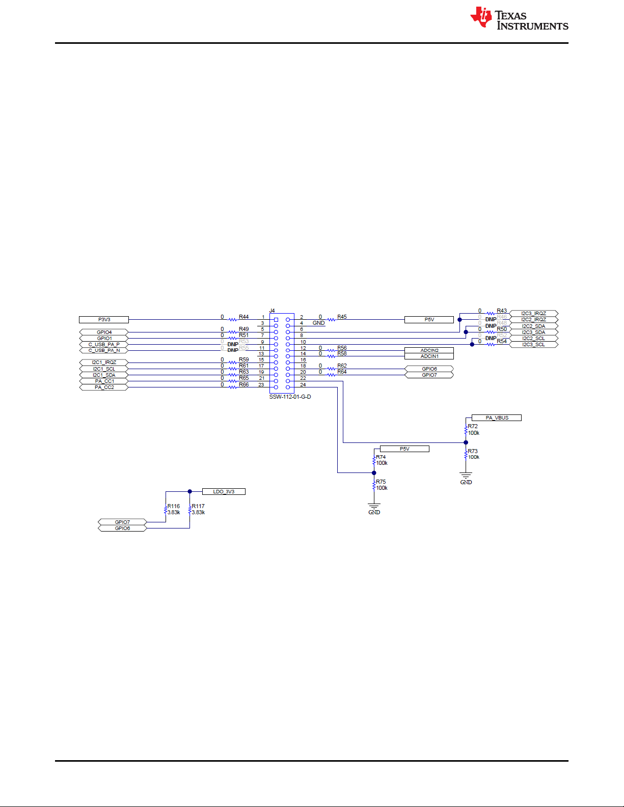
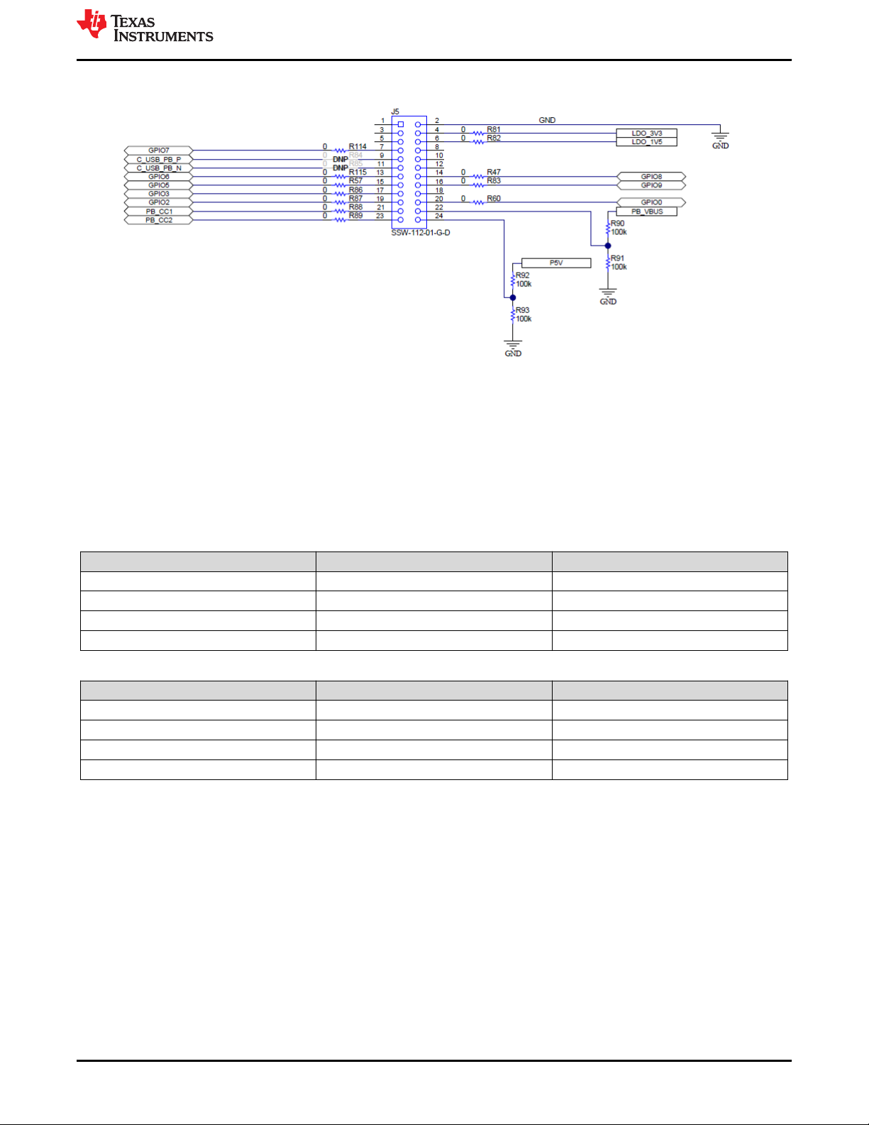
4.1.12 J4 and J5 (Bottom of EVM): Signal Headers
These headers allow the user to probe many different signals on the TPS65994EVM. Note that some of the
header pins are not connected unless a 0-Ω option resistor is placed.
Figure 4-8. Debug Header (J4) Schematic
8 TPS65994 EVM User Guide SLVUBM1C – JANUARY 2019 – REVISED JANUARY 2021
Copyright © 2021 Texas Instruments Incorporated
Submit Document Feedback
Page 9
www.ti.com
Setup
Figure 4-9. Debug Header (J5) Schematic
4.2 LED Indicators Description
The EVM has multiple LEDs to notify the user what type of connection is present. The LEDs are separated into 2
groups: MUX control LEDS and Status LEDs. All LEDs are enabled with general purpose I/O (GPIO); therefore,
each must be enabled separately via configuration, if configuring a custom image
4.2.1 MUX Control LEDs
Table 4-2. Port A MUX CTL LED
LED Indicator GPIO Function
D15 - PA_HPD GPIO1 HPD
D17 - PA_USB3 GPIO3 USB 3.0 Event
D18 - PA_DP_Mode GPIO4 DP Mode Select Event
D23 - PA_POL GPIO9 Cable Orientation Event
Table 4-3. Port B MUX CTL LED
LED Indicator GPIO Function
D14 - PB_HPD GPIO0 HPD
D19 - PB_USB3 GPIO5 USB 3.0 Event
D22 - PB_DP_Mode GPIO8 DP Mode Select Event
D16 - PB_POL GPIO2 Cable Orientation Event
4.2.2 Status LEDs
D1 and D2 LEDs indicate when VBUS voltage is present on port A and port B respectively. They also provide a
voltage discharge path for high to low PD contracts. D4 LED indicates SYS_PWR, when a barrel jack is
connected at J2.
SLVUBM1C – JANUARY 2019 – REVISED JANUARY 2021
Submit Document Feedback
Copyright © 2021 Texas Instruments Incorporated
TPS65994 EVM User Guide 9
Page 10
Tiva USB to I2C Bridge Support Integration
www.ti.com
5 Tiva USB to I2C Bridge Support Integration
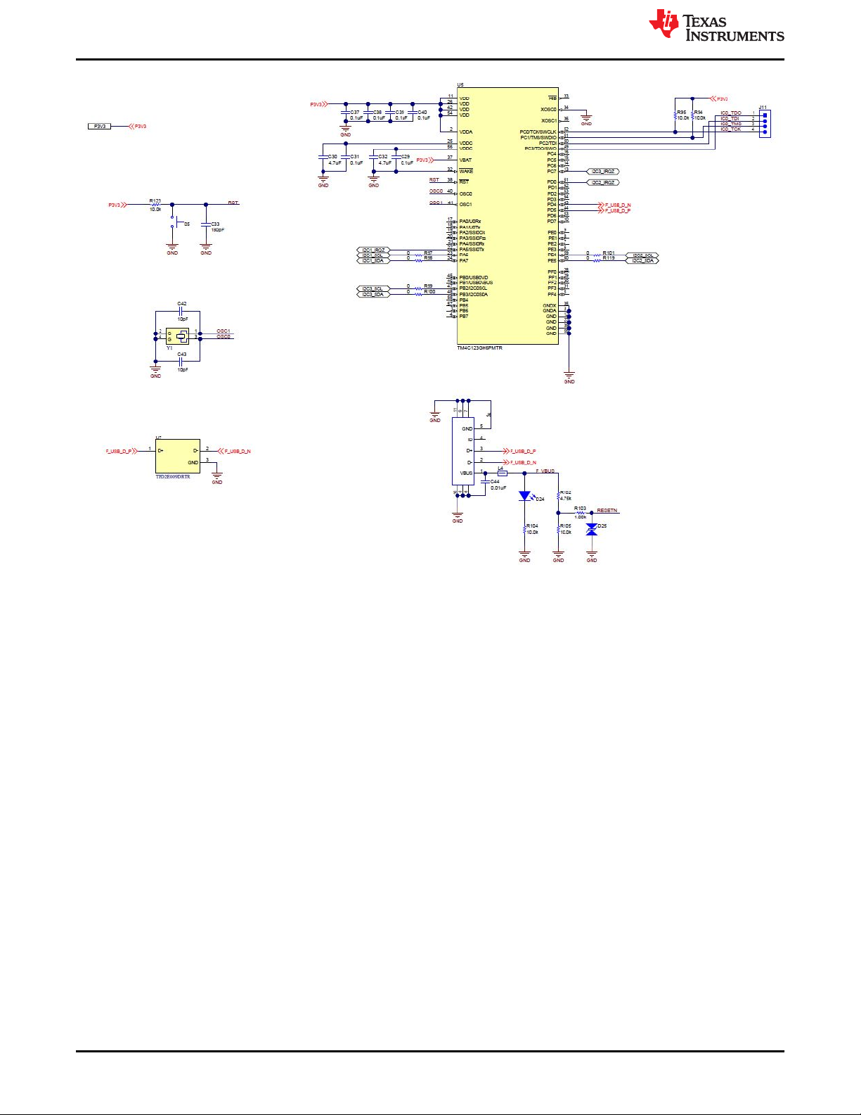
The Tiva microcontroller allows for a reliable USB to I2C connection. This section covers how to flash application
firmware to EEPROM using the Tiva microcontroller and how to enter the debug mode using the Tiva
microcontroller.
5.1 Flash Application Firmware to EEPROM
This section provides the steps to flash the application firmware to EEPROM.
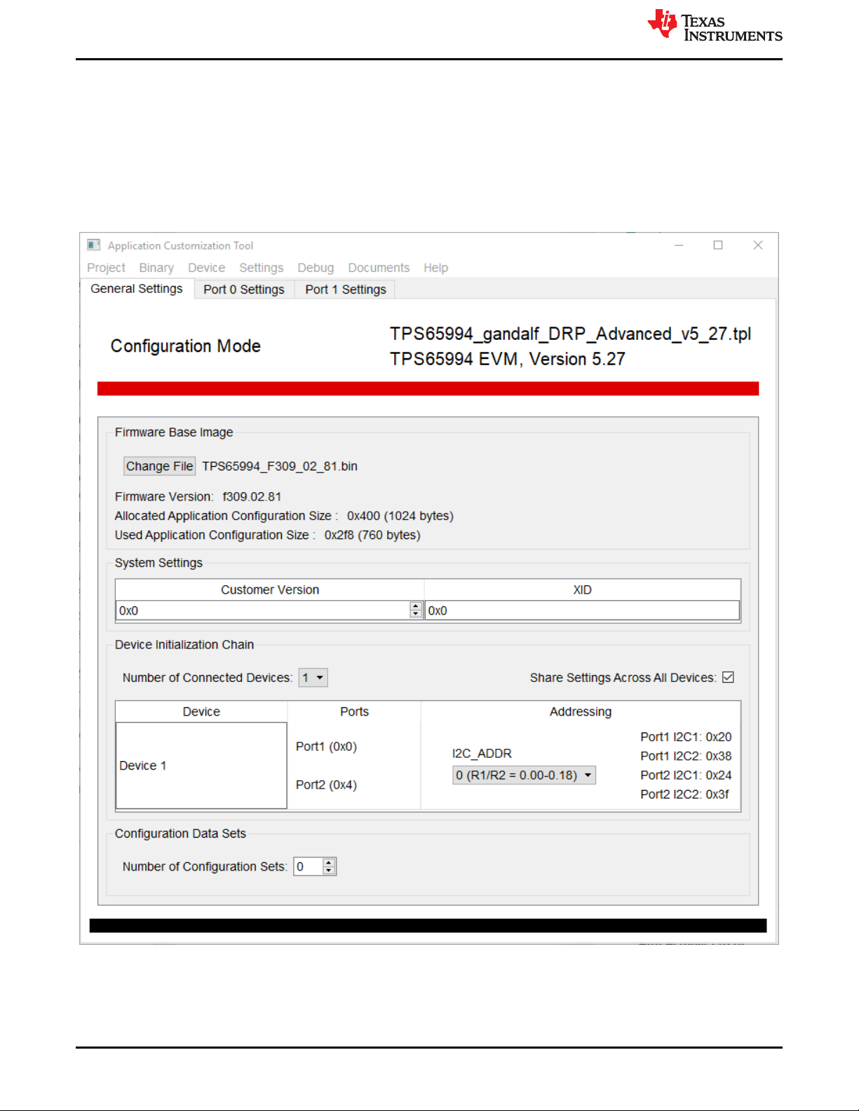
1. Open the Application Customization Tool and Start a New Project
Figure 5-1. Application Customization Tool
10 TPS65994 EVM User Guide SLVUBM1C – JANUARY 2019 – REVISED JANUARY 2021
Copyright © 2021 Texas Instruments Incorporated
Submit Document Feedback
Page 11
www.ti.com
Tiva USB to I2C Bridge Support Integration
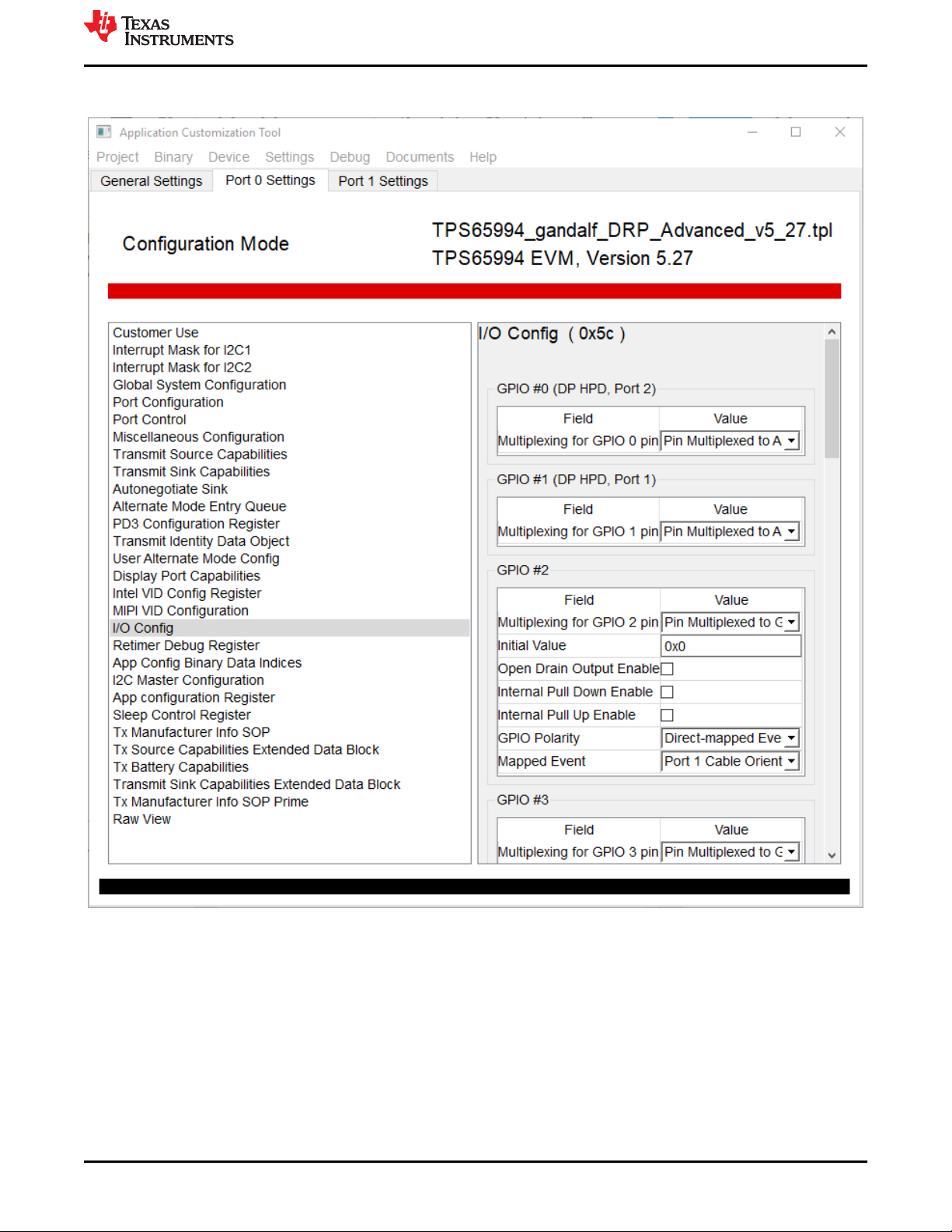
2. Create a project by modifying the registers according to your needs. For example, I/O Config (register 0x5c)
allows for user-defined GPIOs.
SLVUBM1C – JANUARY 2019 – REVISED JANUARY 2021
Submit Document Feedback
Copyright © 2021 Texas Instruments Incorporated
Figure 5-2. I/O Config Register
TPS65994 EVM User Guide 11
Page 12
Tiva USB to I2C Bridge Support Integration
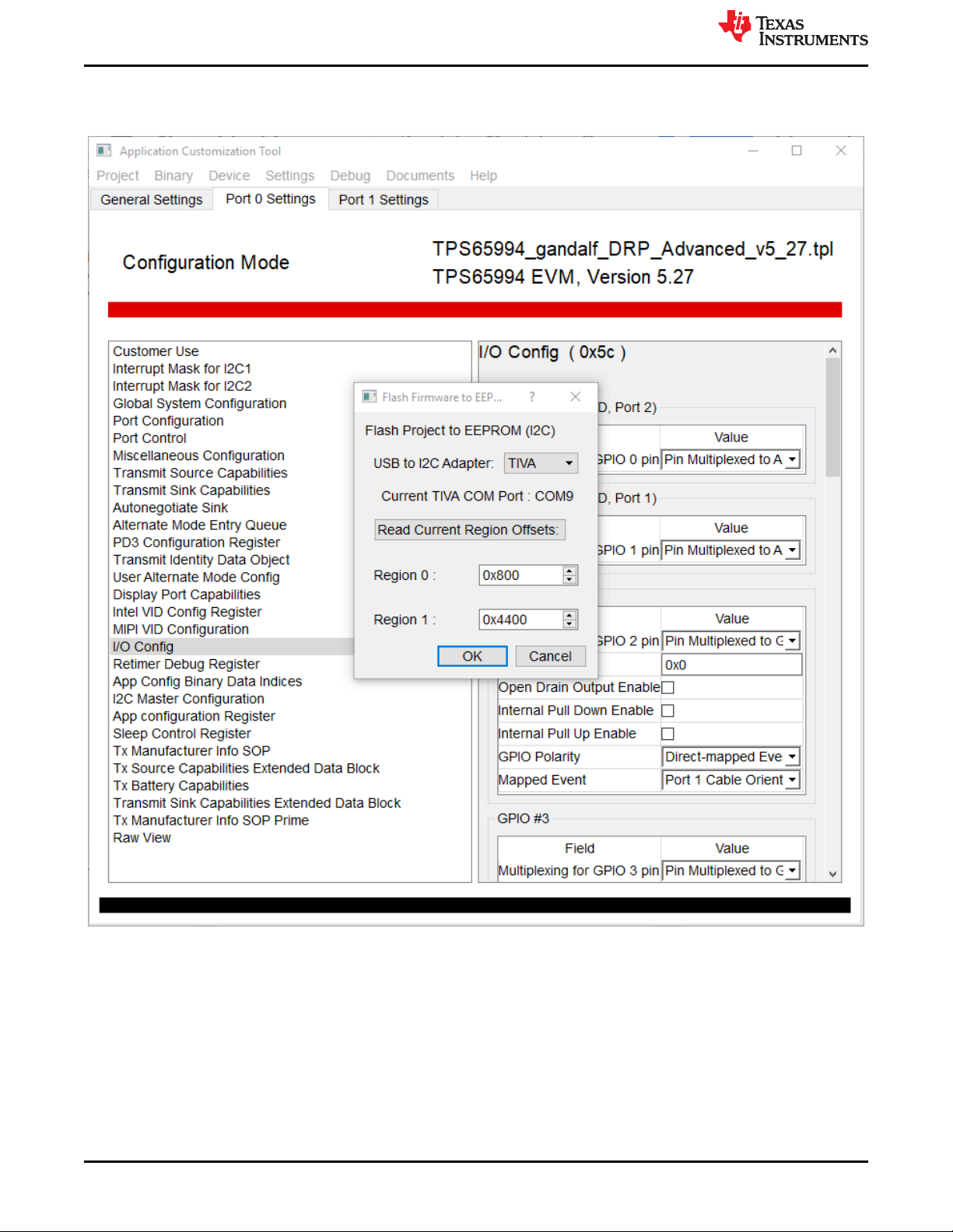
3. After defining the registers, use the Device tab and flash app firmware to EEPROM to load the new
configurations to the device. Ensure that the correct adapter is selected. For this case, select the Tiva
adapter.
www.ti.com
Figure 5-3. Flash Project to EEPROM (I2C)
12 TPS65994 EVM User Guide SLVUBM1C – JANUARY 2019 – REVISED JANUARY 2021
Copyright © 2021 Texas Instruments Incorporated
Submit Document Feedback
Page 13
www.ti.com
Tiva USB to I2C Bridge Support Integration
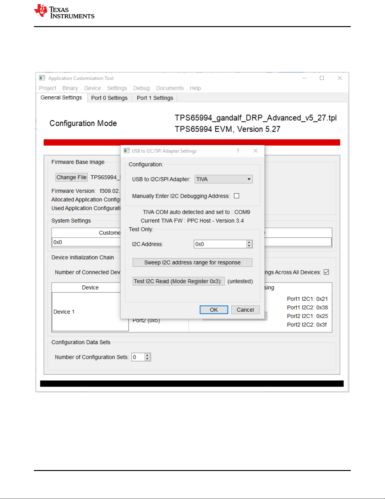
5.2 Entering Debug Mode
This section provides the steps for using Debug mode.
1. Ensure the USB to I2C/SPI adapter is selected accordingly with the device being used. In this case select the
Tiva adapter. Sweep I2C address range to discover the port addresses.
Figure 5-4. USB to I2C/SPI Adapter Settings
SLVUBM1C – JANUARY 2019 – REVISED JANUARY 2021
Submit Document Feedback
Copyright © 2021 Texas Instruments Incorporated
TPS65994 EVM User Guide 13
Page 14
Tiva USB to I2C Bridge Support Integration
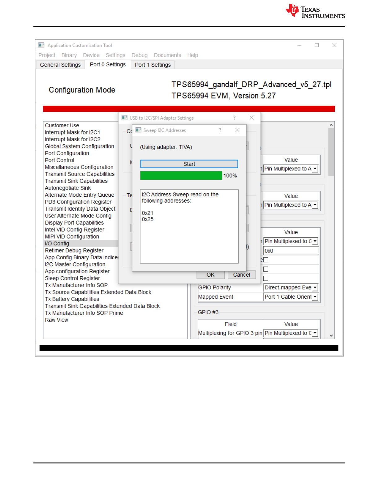
2. I2C address sweep results.
www.ti.com
Figure 5-5. I2C Addresses
14 TPS65994 EVM User Guide SLVUBM1C – JANUARY 2019 – REVISED JANUARY 2021
Copyright © 2021 Texas Instruments Incorporated
Submit Document Feedback
Page 15
www.ti.com
Tiva USB to I2C Bridge Support Integration
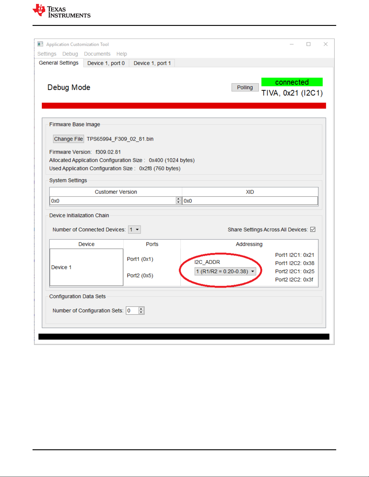
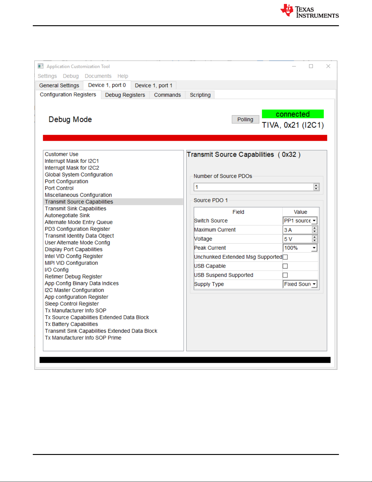
3. Once on debug mode, ensure that I2C_ADDR is within the required range for the addresses.
SLVUBM1C – JANUARY 2019 – REVISED JANUARY 2021
Submit Document Feedback
Copyright © 2021 Texas Instruments Incorporated
Figure 5-6. Addressing range
TPS65994 EVM User Guide 15
Page 16
Tiva USB to I2C Bridge Support Integration
www.ti.com
4. Ensure that the registers are defined as expected by navigating through the Configuration Registers tab. The
Debug Registers tab provides the run-time information on the registers. Finally, the Commands tab allows for
the execution of defined commands in run-time. The following example shows the Transmit Source
Capabilities (register 0x32) information.
Figure 5-7. Transmit Source Capabilities
For more information about how to use the Application Customization Tool, refer to the GUI user's guide.
16 TPS65994 EVM User Guide SLVUBM1C – JANUARY 2019 – REVISED JANUARY 2021
Copyright © 2021 Texas Instruments Incorporated
Submit Document Feedback
Page 17

www.ti.com
Using the TPS65994EVM
6 Using the TPS65994EVM
This section discusses the pre-loaded or recovery firmware, getting started, and debugging the EVM.
6.1 Powering the TPS65994EVM
The main power supply for the EVM is the barrel jack (J2), which accepts 19 V to 20 V via a barrel jack adapter.
The EVM can also be powered with an external power supply on SYS_PWR (TP7). The input voltage can range
from 5 V to 20 V, but the appropriate power profile for PP_EXT should be configured in the firmware using the
configuration tool. The EVM can also be bus-powered from the USB Type-C connector and accepts 5 V to 20 V
on VBUS, depending on the sink configuration.
6.2 Firmware Configurations
Out of the box, the TPS65994EVM is configured to emulate a dual-port laptop computer. For each port, the
internal power switch is configured for sourcing, and the external high current power switch is configured for
sinking. Both ports are configured for data DFP.
SLVUBM1C – JANUARY 2019 – REVISED JANUARY 2021
Submit Document Feedback
Copyright © 2021 Texas Instruments Incorporated
TPS65994 EVM User Guide 17
Page 18

Connecting the EVM
www.ti.com
7 Connecting the EVM
7.1 Connecting to Various Devices
Various USB Type-C cables can be used to connect the EVM to a legacy Type-A device, legacy Type-A host, or
USB Type-C device or host.
7.1.1 Connecting to a Legacy Type-A Device
Using a USB Type-C to Type-A cable allows for connection to a legacy USB device, such as a flash-drive. The
TPS65994 can act as a host passing the DP or USB connection by using the SS MUX and USB HUB present on
the DP-Expansion board.. Figure Below shows how the notebook, DP and USB receptacle, TPS65988EVM,
cable, and flash drive are connected.
7.1.2 Connecting to USB Type-C™ Devices
Using a USB Type-C cable allows for connection to USB and DP devices. When a TPS65994EVM is used with a
TPS6598x-EVM as DP source and sink boards respectively, a complete USB Type-C system can be verified.
The test setup requires a DP and USB source to provide data to the sink board, and a DP-Expansion board. A
DP monitor and USB device can now be connected to the sink board. Note that USB and DisplayPort video
quality may degrade due to the use of multiple connectors and cables. Figure Below highlights this feature.
7.1.3 Testing DisplayPort Alternate Mode and USB 2.0 and USB 3.0
The DisplayPort alternate mode can be tested with a non-USB Type-C notebook, allowing the user to simulate a
DisplayPort DFP_D (video source) or UFP_D (video sink).
7.1.3.1 Required Hardware
The following hardware is required to test the DP alternate mode and USB 3.0:
• A Microsoft® Windows® PC with a USB Type-A receptacle and DisplayPort video output
– USB 2.0 or USB 3.0 Type-A to Type-B cable
– USB 2.0 or USB 3.0, or USB Type-C flash drive
– USB 2.0 Type-A to micro USB cable
• USB Type-C cable
• Monitor with DisplayPort Input
• Mini DisplayPort to DisplayPort cable or USB Type-C to DisplayPort cable
• FTDI board (used for programming the TPS695994EVM and interfacing with configuration tool)
• Dell laptop power supply (model # 492-BBGP)
Use the TPS65994EVM with a DP-Expansion board to test DP alternate mode as well as USB data using the
default firmware. To do so, connect a DP source from a laptop to the TPS65994EVM through the DP-Expansion
Board. Next, connect a USB Type-B to USB Type-A cable from the TPS65994EVM to a Windows computer. To
test DP, connect a mini-DP to DP cable to a monitor from the DP-Expansion board, and a USB Type-C to USB
Type-C cable from laptop to TPS65994EVM. To test USB functionality, either connect a USB Type-C flash drive
to the other USB Type-C port on the TPS65994EVM or plug in a Type-A flash drive on the DP-EXPANSIONEVM. The monitor displays what is present from the DP source. The flash drive enumerates on the windows PC.
Table 7 explains this test setup.
18 TPS65994 EVM User Guide SLVUBM1C – JANUARY 2019 – REVISED JANUARY 2021
Copyright © 2021 Texas Instruments Incorporated
Submit Document Feedback
Page 19

www.ti.com
Debugging the EVM
8 Debugging the EVM
This section discusses various debugging examples. Testing and debugging approaches on the EVM can be
applied to an actual system to help identify any issues.
8.1 Connection Not Established
The following checks help resolve issues when connecting the EVM to another EVM or USB Type-C device and
no status LEDs are on:
• Verify that a firmware image is loaded in on the TPS65994 using the TPS65994 Configuration Tool
• Verify the CC lines are toggling for Dual-Role Port functionality
• Verify the following system supplies:
– System_3V3 and VIN_3V3: 3.3 V
– System_5V : 5 V
– Barrel jack and SYS_PWR: 20 V
– LDO_3V3: 3.3 V
• Verify that the devices connected are compatible. The following are some of the compatible connections:
– Dual-Role Port → UFP
– Dual-Role Port → DFP
– DFP → UFP
• Verify that VBUS is reaching 5 V when connected
8.2 Resetting Behavior
Improper configurations and shorts can cause a USB Type-C PD system to constantly reset. The following
checks should be used to debug these types of issues:
• Verify that the essential power paths have the correct voltages:
– System_3V3 and System_5V
– System Power: 20 V (or the appropriate configured voltage)
• Probe VBUS, CC1, and CC2 to check for any anomalies.
• When there is a short on VBUS, the initial 5 V on VBUS is not present
• Check for a small spike on VBUS during a plug event to verify that the PP or PP_EXT switch is closed and is
then opened, once an overcurrent condition is detected.
SLVUBM1C – JANUARY 2019 – REVISED JANUARY 2021
Submit Document Feedback
Copyright © 2021 Texas Instruments Incorporated
TPS65994 EVM User Guide 19
Page 20

TPS65994EVM Schematics
9 TPS65994EVM Schematics
Figure 9-1 through Figure 9-7 show the TPS65994EVM schematics.
www.ti.com
Figure 9-1. TPS65994EVM Block Diagram
20 TPS65994 EVM User Guide SLVUBM1C – JANUARY 2019 – REVISED JANUARY 2021
Copyright © 2021 Texas Instruments Incorporated
Submit Document Feedback
Page 21

SYS_P WR
IMax = 3A
SYS_PWR
GNDGND
TVS Diode for faulty barrel jacks
GND GND
Used for GND return for high currents
GND
SYS_PWR LED Indicator
21
Blue
D4
CS1
1
VFB1
2
VREG3
3
VFB2
4
CS2
5
EN2
6
PGOOD
7
SW2
8
VBST2
9
DRVH2
10
DRVL2
11
VIN
12
VREG5
13
VO1
14
DRVL1
15
DRVH1
16
VBST1
17
SW1
18
VCLK
19
EN1
20
GND
21
TPS51225RUKR
U3
3.3uH
L1
2.2
R29
15.4k
R32
10.0k
R36
10.0k
R37
6.49k
R31
GND GND
2.2uH
L2
GNDGND
0.1uF
C14
2.2
R30
0.1uF
C15
GNDGND
51.1k
R34
47.5k
R35
GNDGND GND
PWR_EN
PWR_EN
P3V3P5V
IMax = 8A
GND
PGOOD
4.7uF
C22
GND
4.7uF
C21
GND
GND
P5V0
3V3_LDO_EN
3V3_LDO_EN
3
1
5
9 2
47
6
8
Q3
CSD87330Q3D
3
1
5
9 2
4 7
6
8
Q4
CSD87330Q3D
6.3V
100uF
C20
6.3V
100uF
C19
SYS_PWR
6.3V
100uF
C17
6.3V
100uF
C16
GND
100k
R113
TP7
TP8
TP10 TP11
TP13TP12
0R33
0R112
10.0k
R38
D3
GND
P3V3
GND
P5V
22uF
C12
22uF
C13
22uF
C10
22uF
C11
47uF
C46
47uF
C47
47uF
C18
47uF
C45
SENSE
1
GND
4
POWER
2
POWER
3
GND
5
SHIELD
6
SHIELD
7
SHIELD
8
SHIELD
9
J2
JPD1135-509 -7F
GND
Texas Instruments NDA Restrictions
PWR_EN
0
R39
0
R118
www.ti.com
TPS65994EVM Schematics
SLVUBM1C – JANUARY 2019 – REVISED JANUARY 2021
Submit Document Feedback
Figure 9-2. TPS65994EVM PD Controller
Figure 9-3. TPS65994EVM Power Supplies
Copyright © 2021 Texas Instruments Incorporated
TPS65994 EVM User Guide 21
Page 22
TPS65994EVM Schematics www.ti.com
22 TPS65994 EVM User Guide SLVUBM1C – JANUARY 2019 – REVISED JANUARY 2021
Copyright © 2021 Texas Instruments Incorporated
Submit Document Feedback
Page 23
www.ti.com
TPS65994EVM Schematics
Figure 9-4. TPS65994EVM USB Type-C™ Connector
SLVUBM1C – JANUARY 2019 – REVISED JANUARY 2021
Submit Document Feedback
Copyright © 2021 Texas Instruments Incorporated
TPS65994 EVM User Guide 23
Page 24
TPS65994EVM Schematics
www.ti.com
Figure 9-5. TPS65994EVM Tiva Debug
24 TPS65994 EVM User Guide SLVUBM1C – JANUARY 2019 – REVISED JANUARY 2021
Copyright © 2021 Texas Instruments Incorporated
Submit Document Feedback
Page 25
www.ti.com
TPS65994EVM Schematics
Figure 9-6. TPS65994EVM Connectors
SLVUBM1C – JANUARY 2019 – REVISED JANUARY 2021
Submit Document Feedback
Copyright © 2021 Texas Instruments Incorporated
TPS65994 EVM User Guide 25
Page 26
TPS65994EVM Schematics
www.ti.com
Figure 9-7. TPS65994EVM Expansion Connector
26 TPS65994 EVM User Guide SLVUBM1C – JANUARY 2019 – REVISED JANUARY 2021
Copyright © 2021 Texas Instruments Incorporated
Submit Document Feedback
Page 27

www.ti.com
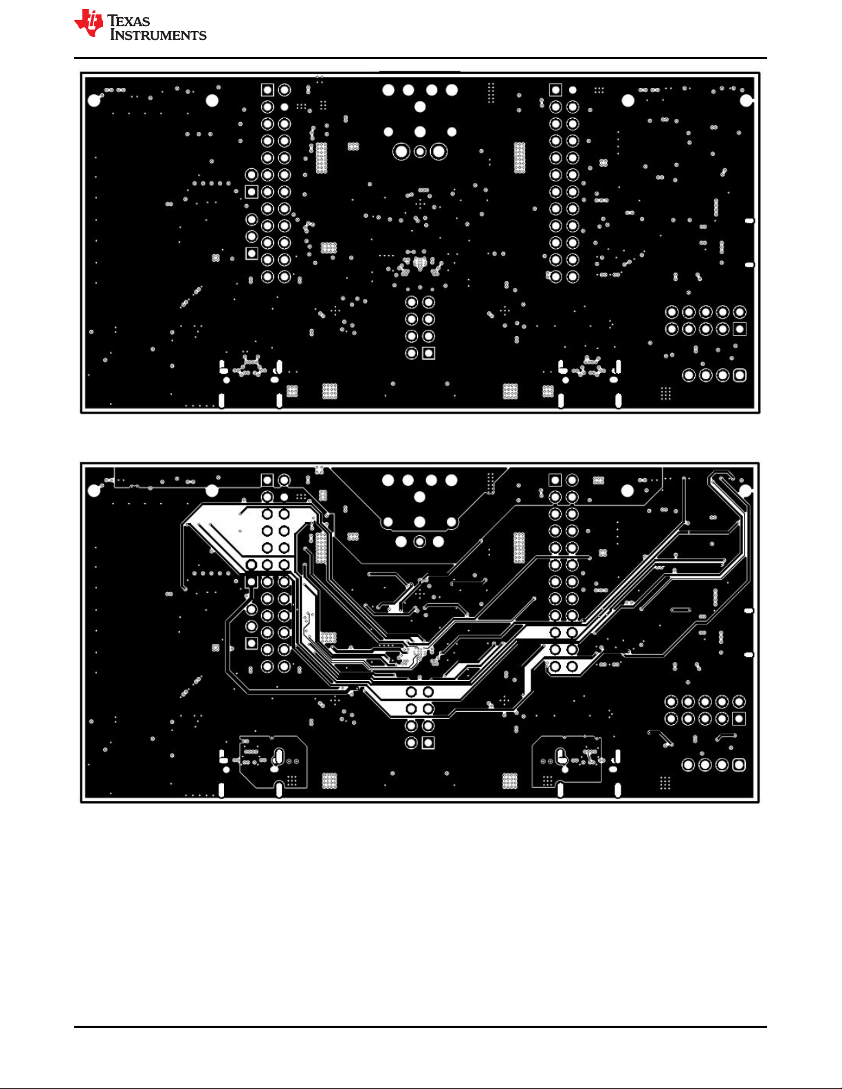
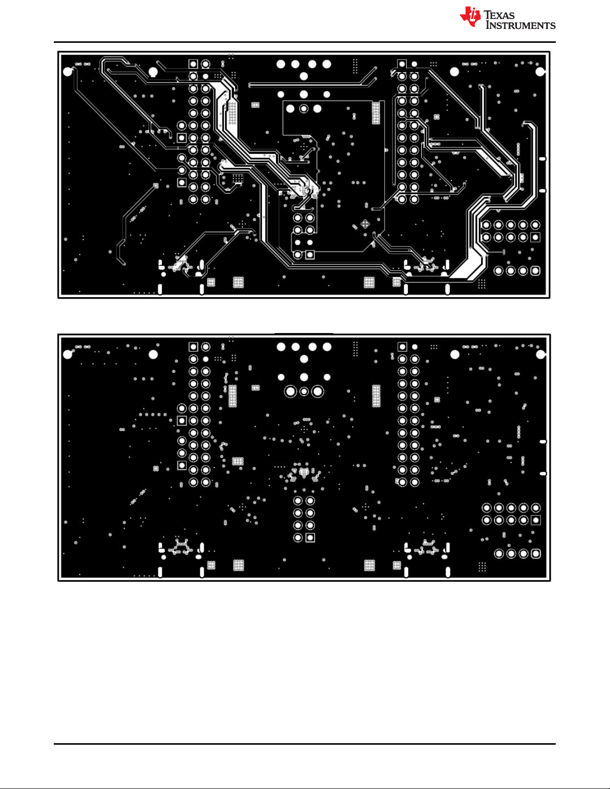
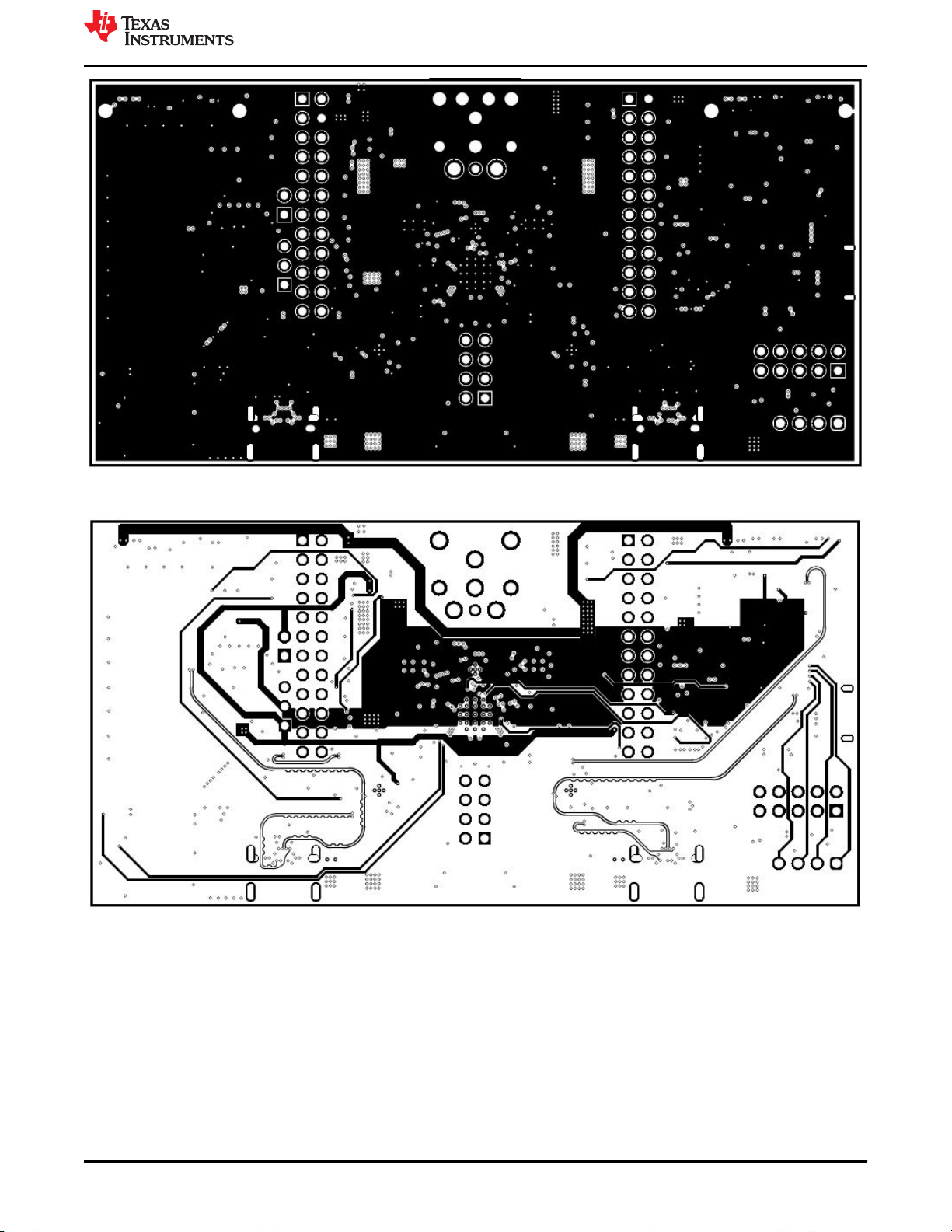
10 TPS65994EVM Board Layout
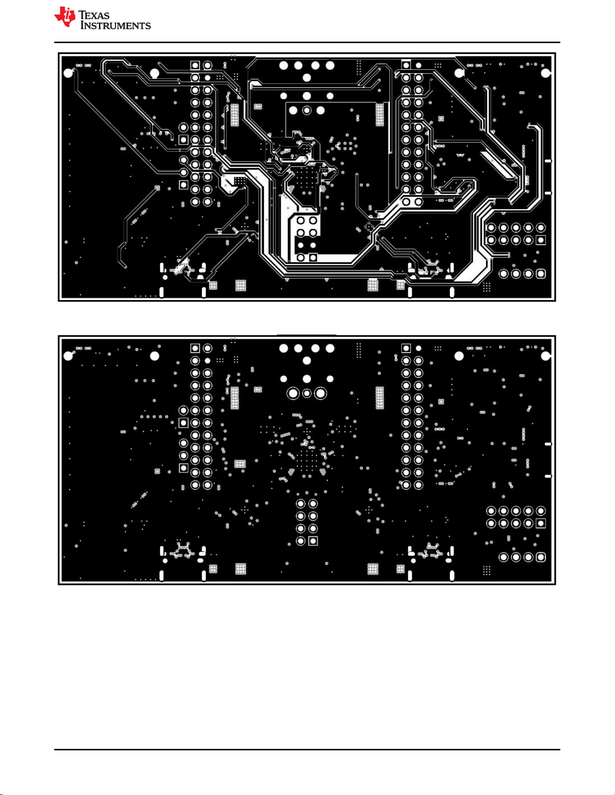
Figure 10-1 through Figure 10-10 show the TPS65994EVM board layout images.
TPS65994EVM Board Layout
Figure 10-1. TPS65994EVM Top Silk Screen
Figure 10-2. TPS65994EVM Top Layer
SLVUBM1C – JANUARY 2019 – REVISED JANUARY 2021
Submit Document Feedback
Copyright © 2021 Texas Instruments Incorporated
TPS65994 EVM User Guide 27
Page 28

TPS65994EVM Board Layout
www.ti.com
Figure 10-3. TPS65994EVM GND Plane 1
Figure 10-4. TPS65994EVM High Speed Layer
28 TPS65994 EVM User Guide SLVUBM1C – JANUARY 2019 – REVISED JANUARY 2021
Copyright © 2021 Texas Instruments Incorporated
Submit Document Feedback
Page 29
www.ti.com
TPS65994EVM Board Layout
Figure 10-5. TPS65994EVM GND Plane 2
Figure 10-6. TPS65994EVM Power 1 Layer
SLVUBM1C – JANUARY 2019 – REVISED JANUARY 2021
Submit Document Feedback
Copyright © 2021 Texas Instruments Incorporated
TPS65994 EVM User Guide 29
Page 30
TPS65994EVM Board Layout
www.ti.com
Figure 10-7. TPS65994EVM Power 2 Layer
Figure 10-8. TPS65994EVM GND Plane 3
30 TPS65994 EVM User Guide SLVUBM1C – JANUARY 2019 – REVISED JANUARY 2021
Copyright © 2021 Texas Instruments Incorporated
Submit Document Feedback
Page 31

www.ti.com
TPS65994EVM Board Layout
Figure 10-9. TPS65994EVM Bottom Layer
Figure 10-10. TPS65994EVM Bottom Silk Screen
SLVUBM1C – JANUARY 2019 – REVISED JANUARY 2021
Submit Document Feedback
Copyright © 2021 Texas Instruments Incorporated
TPS65994 EVM User Guide 31
Page 32

TPS65994EVM Bill of Materials www.ti.com
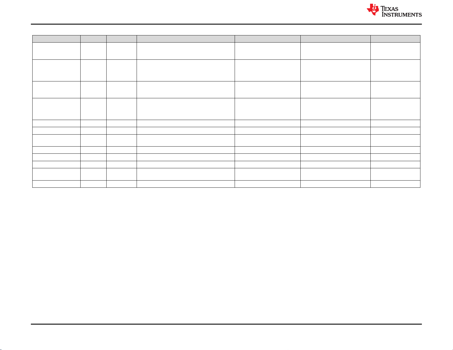
11 TPS65994EVM Bill of Materials
Table 11-1 lists the TPS65994EVM bill of materials.
Table 11-1. TPS65994EVM BOM
Designator QTY Value Description Package Reference Part Number Manufacturer
!PCB1 1 Printed Circuit Board PSIL053 Any
C1, C2, C6, C7 4 220pF CAP, CERM, 220 pF, 50 V, +/- 10%, X7R, AEC-Q200
C3, C8 2 10uF CAP, CERM, 10 uF, 25 V, +/- 20%, X5R, 0603 0603 GRM188R61E106MA73D MuRata
C4, C5, C50 3 10uF CAP, CERM, 10 uF, 10 V, +/- 20%, X5R, 0402 0402 CL05A106MP5NUNC Samsung Electro-Mechanics
C9, C29, C31, C37, C38,
C39, C40
C10, C11, C12, C13 4 22uF CAP, CERM, 22 uF, 35 V, +/- 20%, X5R, 0805 0805 C2012X5R1V226M125AC TDK
C14, C15 2 0.1uF CAP, CERM, 0.1 uF, 35 V, +/- 10%, X5R, 0402 0402 GMK105BJ104KV-F Taiyo Yuden
C16, C17, C19, C20 4 100uF CAP, TA, 100 uF, 6.3 V, +/- 20%, 0.015 ohm, SMD 3528-21 T520B107M006ATE015 Kemet
C18, C45, C46, C47 4 47uF CAP, CERM, 47 uF, 10 V, +/- 20%, X5R, 1206 1206 C3216X5R1A476M160AB TDK
C21, C22 2 4.7uF CAP, CERM, 4.7 uF, 6.3 V, +/- 20%, X5R, 0402 0402 GRM155R60J475ME87D MuRata
C23_PA, C23_PB,
C24_PA, C24_PB,
C25_PA, C25_PB,
C26_PA, C26_PB, C44
C27_PA, C27_PB 2 1uF CAP, CERM, 1 uF, 6.3 V, +/- 20%, X5R, 0201 0201 GRM033R60J105MEA2D MuRata
C28_PA, C28_PB 2 0.1uF CAP, CERM, 0.1 uF, 100 V,+/- 10%, X7R, AEC-Q200
C30, C32 2 4.7uF CAP, CERM, 4.7 uF, 10 V, +/- 20%, X5R, 0402 0402 C1005X5R1A475M050BC TDK
C33 1 180pF CAP, CERM, 180 pF, 50 V, +/- 5%, C0G/NP0, 0603 0603 06035A181JAT2A AVX
C34_PA, C34_PB 2 4.7uF CAP, CERM, 4.7 uF, 35 V, +/- 10%, X5R, 0603 0603 GRM188R6YA475KE15D MuRata
C42, C43 2 10pF CAP, CERM, 10 pF, 50 V, +/- 5%, C0G/NP0, 0603 0603 06035A100JAT2A AVX
C48, C52 2 1uF CAP, CERM, 1 uF, 35 V, +/- 10%, X5R, 0402 0402 GRM155R6YA105KE11D MuRata
D1, D2, D14, D15, D16,
D17, D18, D19, D20,
D21, D22, D23, D24
D3 1 24V Diode, TVS, Bi, 24 V, 70 Vc, SOD323, 2-Leads, Body
D4 1 Blue LED, Blue, SMD LED_0603 150060BS75000 Wurth Elektronik
D5_PA, D5_PB 2 30V Diode, Schottky, 30 V, 2 A, 2-XFDFN 2-XFDFN NSR20F30NXT5G ON Semiconductor
D6_PA, D6_PB, D7_PA,
D7_PB, D8_PA, D8_PB,
D9_PA, D9_PB, D10_PA,
D10_PB, D11_PA,
D11_PB, D12_PA,
D12_PB, D13_PA,
D13_PB
7 0.1uF CAP, CERM, 0.1 uF, 50 V, +/- 10%, X7R, 0402 0402 C1005X7R1H104K050BB TDK
9 0.01uF CAP, CERM, 0.01 uF, 50 V, +/- 5%, X7R, 0402 0402 C0402C103J5RACTU Kemet
13 White LED, White, SMD 0402, White LW QH8G-Q2S2-3K5L-1 OSRAM
16 1-Channel ESD Protection Diode for USB Type-C and
Grade 1, 0201
Grade 1, 0603
1.9x1.45mm, No Polarity Mark
Thunderbolt 3, DPL0002A (X2SON-2)
0201 CGA1A2X7R1H221K030BA TDK
0603 GCJ188R72A104KA01D MuRata
SOD323, 2-Leads, Body
1.9x1.45mm, No Polarity Mark
DPL0002A TPD1E01B04DPLR Texas Instruments
PESD24VL1BA,115 NXP Semiconductor
32 TPS65994 EVM User Guide SLVUBM1C – JANUARY 2019 – REVISED JANUARY 2021
Copyright © 2021 Texas Instruments Incorporated
Submit Document Feedback
Page 33

www.ti.com TPS65994EVM Bill of Materials
Table 11-1. TPS65994EVM BOM (continued)
Designator QTY Value Description Package Reference Part Number Manufacturer
D25 1 1-Channel ESD Protection Diode With Low Dynamic
J1 1 Receptacle, 2.54mm, 4x2, Gold, TH Receptacle, 2.54mm, 4x2, TH SSQ-104-03-G-D Samtec
J2 1 Connector, DC Power Jack, R/A, 3 Pos, TH Power connector JPD1135-509-7F Foxconn
J3_PA, J3_PB 2 Receptacle, USB 3.1 Type C, R/A, Gold, SMT Receptacle, USB 3.1 Type C,
J4, J5 2 Receptacle, 12x2, 2.54mm, Gold, TH Receptacle, 12x2, 2.54mm, TH SSW-112-01-G-D Samtec
J6 1 Connector, Receptacle, USB Micro B, R/A, SMT Connector, Receptacle, USB
J7, J8 2 Socket, 0.8mm, 20x2, Gold, SMT Socket, 0.8mm, 20x2, Gold,
J9 1 Header, 100mil, 5x2, Tin, TH Header, 5x2, 100mil, Tin PEC05DAAN Sullins Connector Solutions
J10 1 Header, 100mil, 3x1, Tin, TH Header, 3 PIN, 100mil, Tin PEC03SAAN Sullins Connector Solutions
J11 1 Header, 2.54 mm, 4x1, Gold, TH Header, 2.54mm, 4x1, TH 61300411121 Wurth Elektronik
J12 1 Header, 100mil, 2x1, Gold, TH Sullins 100mil, 1x2, 230 mil
L1 1 3.3uH Inductor, Shielded Drum Core, Superflux, 3.3 uH, 8 A,
L2 1 2.2uH Inductor, Shielded Drum Core, Powdered Iron, 2.2 uH, 3.25
L3_PA, L3_PB 2 22 ohm Ferrite Bead, 22 ohm @ 100 MHz, 6 A, 0805 0805 742792021 Wurth Elektronik
L4 1 26 ohm Ferrite Bead, 26 ohm @ 100 MHz, 6.5 A, 0603 0603 74279228260 Wurth Elektronik
LBL1 1 Thermal Transfer Printable Labels, 0.650" W x 0.200" H -
Q1, Q2 2 30V MOSFET, 2-CH, N-CH, 30 V, A, YJG0010A
Q3, Q4 2 30V MOSFET, 2-CH, N-CH, 30 V, 20 A, DQZ0008A (LSON-
Q5, Q6, Q7, Q8, Q9,
Q10, Q11, Q12, Q13,
Q14
R1, R14, R67, R68, R69,
R70, R71, R76, R77,
R78, R79, R80, R96
R2, R3, R5, R6, R8, R9 6 2.20k RES, 2.20 k, 1%, 0.05 W, 0201 0201 CRCW02012K20FKED Vishay-Dale
R4, R7, R10, R21, R23,
R24, R25
R11, R20 2 499k RES, 499 k, 1%, 0.063 W, AEC-Q200 Grade 0, 0402 0402 CRCW0402499KFKED Vishay-Dale
R12, R22 2 59.0k RES, 59.0 k, 1%, 0.063 W, AEC-Q200 Grade 0, 0402 0402 CRCW040259K0FKED Vishay-Dale
R13, R26 2 249k RES, 249 k, 1%, 0.063 W, AEC-Q200 Grade 0, 0402 0402 CRCW0402249KFKED Vishay-Dale
R15, R27 2 976k RES, 976 k, 1%, 0.063 W, AEC-Q200 Grade 0, 0402 0402 CRCW0402976KFKED Vishay-Dale
R16, R28 2 40.2k RES, 40.2 k, 1%, 0.063 W, AEC-Q200 Grade 0, 0402 0402 CRCW040240K2FKED Vishay-Dale
10 20V MOSFET, N-CH, 20 V, 0.5 A, YJM0003A (PICOSTAR-3) YJM0003A CSD15380F3 Texas Instruments
13 10k RES, 10 k, 5%, 0.063 W, AEC-Q200 Grade 0, 0402 0402 CRCW040210K0JNED Vishay-Dale
7 10.0k RES, 10.0 k, 1%, 0.05 W, 0201 0201 CRCW020110K0FKED Vishay-Dale
Resistance and Low Clamping Voltage, DPY0002A
(X1SON-2)
0.0096 ohm, SMD
A, 0.051 ohm, SMD
10,000 per roll
(PICOSTAR-10)
CLIP-8)
DPY0002A TPD1E1B04DPYR Texas Instruments
DX07S024JJ2R1300 JAE Electronics
R/A, SMT
10118193-0001LF FCI
Micro B, R/A, SMT
LSEM-120-03.0-F-DV-A-N-K-TR Samtec
SMT
PBC02SAAN Sullins Connector Solutions
above insulator
6.9x4.8x6.9mm 744314330 Wurth Elektronik
4.45x1.8x4.06mm 74437324022 Wurth Elektronik
PCB Label 0.650 x 0.200 inch THT-14-423-10 Brady
YJG0010A CSD87501L Texas Instruments
DQZ0008A CSD87330Q3D Texas Instruments
SLVUBM1C – JANUARY 2019 – REVISED JANUARY 2021
Submit Document Feedback
TPS65994 EVM User Guide 33
Copyright © 2021 Texas Instruments Incorporated
Page 34

TPS65994EVM Bill of Materials www.ti.com
Table 11-1. TPS65994EVM BOM (continued)
Designator QTY Value Description Package Reference Part Number Manufacturer
R29, R30 2 2.2 RES, 2.2, 5%, 0.063 W, AEC-Q200 Grade 0, 0402 0402 CRCW04022R20JNED Vishay-Dale
R31 1 6.49k RES, 6.49 k, 1%, 0.063 W, AEC-Q200 Grade 0, 0402 0402 CRCW04026K49FKED Vishay-Dale
R32 1 15.4k RES, 15.4 k, 1%, 0.063 W, AEC-Q200 Grade 0, 0402 0402 CRCW040215K4FKED Vishay-Dale
R34 1 51.1k RES, 51.1 k, 1%, 0.063 W, AEC-Q200 Grade 0, 0402 0402 CRCW040251K1FKED Vishay-Dale
R35 1 47.5k RES, 47.5 k, 1%, 0.063 W, AEC-Q200 Grade 0, 0402 0402 CRCW040247K5FKED Vishay-Dale
R36, R37, R38, R94,
R95, R104, R105, R123
R39, R41_PA, R41_PB,
R42_PA, R42_PB, R43,
R47, R49, R50, R51,
R54, R56, R57, R58,
R59, R60, R61, R62,
R63, R64, R65, R66,
R81, R82, R83, R86,
R87, R88, R89, R97,
R98, R99, R100, R101,
R114, R115, R118, R119,
R120, R121, R122
R40_PA, R40_PB 2 100k RES, 100 k, 1%, 0.05 W, 0201 0201 CRCW0201100KFKED Vishay-Dale
R73, R75, R91, R93 4 100k RES, 100 k, 1%, 0.1 W, 0603 0603 CRCW0603100KFKEA Vishay-Dale
R102 1 4.75k RES, 4.75 k, 1%, 0.063 W, AEC-Q200 Grade 0, 0402 0402 CRCW04024K75FKED Vishay-Dale
R103 1 1.00k RES, 1.00 k, 1%, 0.063 W, AEC-Q200 Grade 0, 0402 0402 CRCW04021K00FKED Vishay-Dale
R106, R107, R108, R109,
R110, R111
R113 1 100k RES, 100 k, 1%, 0.063 W, AEC-Q200 Grade 0, 0402 0402 CRCW0402100KFKED Vishay-Dale
R116, R117 2 3.83k RES, 3.83 k, 1%, 0.05 W, 0201 0201 CRCW02013K83FKED Vishay-Dale
S1, S2 2 DIP Switch, SPST 4Pos, Slide, SMT 6.2x2.0x6.2mm TDA04H0SB1 C&K Components
S3 1 Switch, Slide, SPST, Top Slide, SMT Switch, Single Top Slide,
S4 1 DIP Switch, SPST, 2Pos, Slide, SMT SW, 4.7x1.45x3mm CVS-02TB Copal Electronics
S5 1 SWITCH TACTILE SPST-NO 0.05A 12V 3x1.6x2.5mm B3U-1000P Omron Electronic Components
SH-J1, SH-J2, SH-J3,
SH-J4, SH-J5, SH-J6
TP1, TP2, TP3, TP4,
TP5, TP6, TP7, TP8,
TP10, TP11, TP12, TP13
U1 1 Dual Port USB Type-C and USB PD Controller with
U2 1 256 kb I2C CMOS Serial EEPROM, SOIC-8 SOIC-8 CAT24C256WI-G ON Semiconductor
U3 1 Dual Synchronous Step-Down Controller with 5-V and 3.3-
U4_PA, U4_PB 2 USB Type-C Port Protector: Short-to-VBUS Overvoltage
8 10.0k RES, 10.0 k, 1%, 0.063 W, AEC-Q200 Grade 0, 0402 0402 CRCW040210K0FKED Vishay-Dale
41 0 RES, 0, 5%, 0.05 W, 0201 0201 CRCW02010000Z0ED Vishay-Dale
6 0 RES, 0, 5%, 0.063 W, AEC-Q200 Grade 0, 0402 0402 CRCW04020000Z0ED Vishay-Dale
CHS-01TB Copal Electronics
2.5x8x2.5mm
6 Shunt, 2.54mm, Gold, Black Shunt, 2.54mm, Black 60900213421 Wurth Elektronik
12 Test Point, Miniature, SMT Test Point, Miniature, SMT 5019 Keystone
DSBGA50 TPS65994ADYBG Texas Instruments
Integrated Source Power Switches
RUK0020B TPS51225RUKR Texas Instruments
V LDOs, RUK0020B (WQFN-20)
RUK0020B TPD6S300ARUKR Texas Instruments
and IEC ESD Protection, RUK0020B (WQFN-20)
34 TPS65994 EVM User Guide SLVUBM1C – JANUARY 2019 – REVISED JANUARY 2021
Copyright © 2021 Texas Instruments Incorporated
Submit Document Feedback
Page 35
www.ti.com TPS65994EVM Bill of Materials
Table 11-1. TPS65994EVM BOM (continued)
Designator QTY Value Description Package Reference Part Number Manufacturer
U5 1 Tiva C Series Microcontroller, 256 KB Flash, 32 KB SRAM,
U6 1 High-Speed USB 2.0 (480 Mbps) 1:2 Multiplexer /
U7 1 ESD Protection Array for High-Speed Data Interfaces, 2
U8_PA, U8_PB 2 22-V Precision Surge Protection Clamp, DRV0006A
Y1 1 Crystal, 16 MHz, 8pF, SMD 3.2x0.75x2.5mm NX3225GA-16.000M-STD-
C49, C51 0 150pF CAP, CERM, 150 pF, 50 V, +/- 10%, X7R, 0201 0201 GRM033R71H151KA12D MuRata
FID1, FID2, FID3, FID4,
FID5, FID6
R17, R18, R19 0 10.0k RES, 10.0 k, 1%, 0.05 W, 0201 0201 CRCW020110K0FKED Vishay-Dale
R33, R112 0 0 RES, 0, 5%, 0.063 W, AEC-Q200 Grade 0, 0402 0402 CRCW04020000Z0ED Vishay-Dale
R44, R45 0 0 RES, 0, 5%, 0.063 W, 0402 0402 CRCW04020000Z0ED Vishay-Dale
R46, R48, R52, R53,
R55, R84, R85
R72, R74, R90, R92 0 100k RES, 100 k, 1%, 0.1 W, 0603 0603 CRCW0603100KFKEA Vishay-Dale
0 Fiducial mark. There is nothing to buy or mount. N/A N/A N/A
0 0 RES, 0, 5%, 0.05 W, 0201 0201 CRCW02010000Z0ED Vishay-Dale
12 Bit, 12 Channels, -40 to 105 degC, 64-Pin LQFP (PM),
Green (RoHS & no Sb/Br), Tape and Reel
Demultiplexer Switch with Single Enable, 6 ohm RON, 2.5
to 3.3V, -40 to 85 degC, 10-Pin UQFN (RSE), Green
(RoHS & no Sb/Br)
Channels, -40 to +85 degC, 3-pin SOT (DRT), Green
(RoHS & no Sb/Br)
(WSON-6)
PM0064A TM4C123GH6PMTR Texas Instruments
RSE0010A TS3USB221RSER Texas Instruments
DRT0003A TPD2E009DRTR Texas Instruments
DRV0006A TVS2200DRVR Texas Instruments
NDK
CRG-1
SLVUBM1C – JANUARY 2019 – REVISED JANUARY 2021
Submit Document Feedback
TPS65994 EVM User Guide 35
Copyright © 2021 Texas Instruments Incorporated
Page 36
TPS65994QFNEVM Schematics
12 TPS65994QFNEVM Schematics
Figure 12-1 through Figure 12-7 illustrate the TPS65994QFNEVM schematics.
www.ti.com
Figure 12-1. TPS65994QFNEVM Block Diagram
36 TPS65994 EVM User Guide SLVUBM1C – JANUARY 2019 – REVISED JANUARY 2021
Copyright © 2021 Texas Instruments Incorporated
Submit Document Feedback
Page 37
www.ti.com
TPS65994QFNEVM Schematics
Figure 12-2. TPS65994QFNEVM PD Controller
SLVUBM1C – JANUARY 2019 – REVISED JANUARY 2021
Submit Document Feedback
Copyright © 2021 Texas Instruments Incorporated
TPS65994 EVM User Guide 37
Page 38
TPS65994QFNEVM Schematics
www.ti.com
Figure 12-3. TPS65994QFNEVM Power Supplies
38 TPS65994 EVM User Guide SLVUBM1C – JANUARY 2019 – REVISED JANUARY 2021
Copyright © 2021 Texas Instruments Incorporated
Submit Document Feedback
Page 39

www.ti.com TPS65994QFNEVM Schematics
SLVUBM1C – JANUARY 2019 – REVISED JANUARY 2021
Submit Document Feedback
Copyright © 2021 Texas Instruments Incorporated
TPS65994 EVM User Guide 39
Page 40

TPS65994QFNEVM Schematics
www.ti.com
Figure 12-4. TPS65994QFNEVM USB Type-C™ Connector
40 TPS65994 EVM User Guide SLVUBM1C – JANUARY 2019 – REVISED JANUARY 2021
Copyright © 2021 Texas Instruments Incorporated
Submit Document Feedback
Page 41

www.ti.com
TPS65994QFNEVM Schematics
Figure 12-5. TPS65994QFNEVM Tiva Debug
SLVUBM1C – JANUARY 2019 – REVISED JANUARY 2021
Submit Document Feedback
Copyright © 2021 Texas Instruments Incorporated
TPS65994 EVM User Guide 41
Page 42
TPS65994QFNEVM Schematics
www.ti.com
Figure 12-6. TPS65994QFNEVM Connectors
42 TPS65994 EVM User Guide SLVUBM1C – JANUARY 2019 – REVISED JANUARY 2021
Copyright © 2021 Texas Instruments Incorporated
Submit Document Feedback
Page 43
www.ti.com
TPS65994QFNEVM Schematics
Figure 12-7. TPS65994QFNEVM Expansion Connector
SLVUBM1C – JANUARY 2019 – REVISED JANUARY 2021
Submit Document Feedback
Copyright © 2021 Texas Instruments Incorporated
TPS65994 EVM User Guide 43
Page 44

TPS65994QFNEVM Board Layout
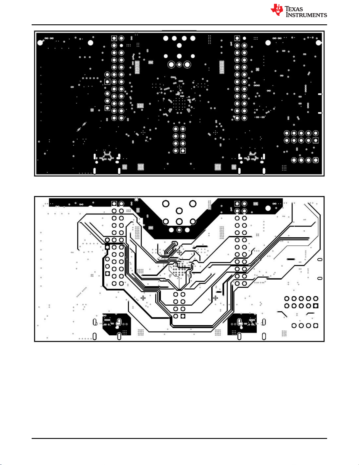
13 TPS65994QFNEVM Board Layout
Figure 13-1 through Figure 13-10 show the TPS65994QFNEVM board layout images.
www.ti.com
Figure 13-1. TPS65994QFNEVM Top Silk Screen
Figure 13-2. TPS65994QFNEVM Top Layer
44 TPS65994 EVM User Guide SLVUBM1C – JANUARY 2019 – REVISED JANUARY 2021
Copyright © 2021 Texas Instruments Incorporated
Submit Document Feedback
Page 45
www.ti.com
TPS65994QFNEVM Board Layout
Figure 13-3. TPS65994QFNEVM GND Plane 1
Figure 13-4. TPS65994QFNEVM High Speed Layer
SLVUBM1C – JANUARY 2019 – REVISED JANUARY 2021
Submit Document Feedback
Copyright © 2021 Texas Instruments Incorporated
TPS65994 EVM User Guide 45
Page 46
TPS65994QFNEVM Board Layout
www.ti.com
Figure 13-5. TPS65994QFNEVM GND Plane 2
Figure 13-6. TPS65994QFNEVM Power 1 Layer
46 TPS65994 EVM User Guide SLVUBM1C – JANUARY 2019 – REVISED JANUARY 2021
Copyright © 2021 Texas Instruments Incorporated
Submit Document Feedback
Page 47
www.ti.com
TPS65994QFNEVM Board Layout
Figure 13-7. TPS65994QFNEVM Power 2 Layer
Figure 13-8. TPS65994QFNEVM GND Plane 3
SLVUBM1C – JANUARY 2019 – REVISED JANUARY 2021
Submit Document Feedback
Copyright © 2021 Texas Instruments Incorporated
TPS65994 EVM User Guide 47
Page 48

TPS65994QFNEVM Board Layout
www.ti.com
Figure 13-9. TPS65994QFNEVM Bottom Layer
Figure 13-10. TPS65994QFNEVM Bottom Silk Screen
48 TPS65994 EVM User Guide SLVUBM1C – JANUARY 2019 – REVISED JANUARY 2021
Copyright © 2021 Texas Instruments Incorporated
Submit Document Feedback
Page 49

www.ti.com TPS65994QFNEVM Bill of Materials
14 TPS65994QFNEVM Bill of Materials
Table 14-1 lists the EVM bill of materials.
Table 14-1. TPS65994QFNEVM Bill of Materials
Designator QTY Value Description Package Reference Part Number Manufacturer
!PCB1 1 Printed Circuit Board PSIL127 Any
C1, C13 2 1uF CAP, CERM, 1 uF, 35 V, ±±10%, X5R, 0402 0402 GRM155R6YA105KE11D MuRata
C3, C4, C8, C9 4 220pF CAP, CERM, 220 pF, 50 V, ±10%, X7R, AEC-Q200
C5, C10, C11 3 10uF CAP, CERM, 10 uF, 10 V, ±20%, X5R, 0402 0402 CL05A106MP5NUNC Samsung Electro-
C6, C7 2 10uF CAP, CERM, 10 uF, 25 V, ±20%, X5R, 0603 0603 GRM188R61E106MA73D MuRata
C14, C38, C39, C40,
C41, C43, C45
C15, C16, C17, C18 4 22uF CAP, CERM, 22 uF, 25 V, ±20%, X5R, 0805 0805 GRM21BR61E226ME44L MuRata
C19, C20 2 0.1uF CAP, CERM, 0.1 uF, 35 V, ±10%, X5R, 0402 0402 GMK105BJ104KV-F Taiyo Yuden
C21, C22, C23, C24 4 100uF CAP, TA, 100 uF, 6.3 V, ±20%, 0.015 ohm, SMD 3528-21 T520B107M006ATE015 Kemet
C25, C26 2 4.7uF CAP, CERM, 4.7 uF, 6.3 V, ±20%, X5R, 0402 0402 GRM155R60J475ME87D MuRata
C27, C28, C29, C30 4 47uF CAP, CERM, 47 uF, 10 V, ±20%, X5R, 1206 1206 C3216X5R1A476M160AB TDK
C31_PA, C31_PB 2 4.7uF CAP, CERM, 4.7 uF, 35 V, ±10%, X5R, 0603 0603 GRM188R6YA475KE15D MuRata
C32_PA, C32_PB,
C33_PA, C33_PB,
C34_PA, C34_PB,
C35_PA, C35_PB, C49
C36_PA, C36_PB 2 1uF CAP, CERM, 1 uF, 6.3 V, ±20%, X5R, 0201 0201 GRM033R60J105MEA2D MuRata
C37_PA, C37_PB 2 0.1uF CAP, CERM, 0.1 uF, 100 V,±10%, X7R, AEC-Q200
C42, C44 2 4.7uF CAP, CERM, 4.7 uF, 10 V, ±20%, X5R, 0402 0402 C1005X5R1A475M050BC TDK
C46 1 180pF CAP, CERM, 180 pF, 50 V, ±5%, C0G/NP0, 0603 0603 06035A181JAT2A AVX
C47, C48 2 10pF CAP, CERM, 10 pF, 50 V, ±5%, C0G/NP0, 0603 0603 06035A100JAT2A AVX
D1, D2, D14, D16, D17,
D18, D19, D20, D21,
D22, D23, D24, D25
D3 1 24V Diode, TVS, Bi, 24 V, 70 Vc, SOD323, 2-Leads, Body
D4 1 Blue LED, Blue, SMD LED_0603 150060BS75000 Wurth Elektronik
D5_PA, D5_PB 2 30V Diode, Schottky, 30 V, 2 A, 2-XFDFN 2-XFDFN NSR20F30NXT5G ON Semiconductor
D6_PA, D6_PB, D7_PA,
D7_PB, D8_PA, D8_PB,
D9_PA, D9_PB, D10_PA,
D10_PB, D11_PA,
D11_PB, D12_PA,
D12_PB, D13_PA,
D13_PB
7 0.1uF CAP, CERM, 0.1 uF, 50 V, ±10%, X7R, AEC-Q200
9 0.01uF CAP, CERM, 0.01 uF, 50 V, ±5%, X7R, 0402 0402 C0402C103J5RACTU Kemet
13 White LED, White, SMD 0402, White LW QH8G-Q2S2-3K5L-1 OSRAM
16 1-Channel ESD Protection Diode for USB Type-C and
Grade 1, 0201
Grade 1, 0402
Grade 1, 0603
1.9x1.45mm, No Polarity Mark
Thunderbolt 3, DPL0002A (X2SON-2)
0201 CGA1A2X7R1H221K030BA TDK
Mechanics
0402 CGA2B3X7R1H104K050BB TDK
0603 GCJ188R72A104KA01D MuRata
SOD323, 2-Leads, Body
1.9x1.45mm, No Polarity Mark
DPL0002A TPD1E01B04DPLR Texas Instruments
PESD24VL1BA,115 NXP Semiconductor
SLVUBM1C – JANUARY 2019 – REVISED JANUARY 2021
Submit Document Feedback
TPS65994 EVM User Guide 49
Copyright © 2021 Texas Instruments Incorporated
Page 50

TPS65994QFNEVM Bill of Materials www.ti.com
Table 14-1. TPS65994QFNEVM Bill of Materials (continued)
Designator QTY Value Description Package Reference Part Number Manufacturer
D15 1 1-Channel ESD Protection Diode With Low Dynamic
J1 1 Header, 100mil, 3x1, Tin, TH Header, 3 PIN, 100mil, Tin PEC03SAAN Sullins Connector
J2 1 Receptacle, 2.54mm, 4x2, Gold, TH Receptacle, 2.54mm, 4x2, TH SSQ-104-03-G-D Samtec
J3 1 Header, 100mil, 2x1, Gold, TH Sullins 100mil, 1x2, 230 mil above
J4 1 Connector, DC Power Jack, R/A, 3 Pos, TH Power connector JPD1135-509-7F Foxconn
J5_PA, J5_PB 2 Receptacle, USB 3.1 Type C, R/A, Gold, SMT Receptacle, USB 3.1 Type C, R/A,
J6 1 Header, 2.54 mm, 4x1, Gold, TH Header, 2.54mm, 4x1, TH 61300411121 Wurth Elektronik
J7 1 Connector, Receptacle, USB Micro B, R/A, SMT Connector, Receptacle, USB Micro
J8, J9 2 Socket, 0.8mm, 20x2, Gold, SMT Socket, 0.8mm, 20x2, Gold, SMT LSEM-120-03.0-F-DV-A-N-K-TR Samtec
J10, J11 2 Receptacle, 12x2, 2.54mm, Gold, TH Receptacle, 12x2, 2.54mm, TH SSW-112-01-G-D Samtec
J12 1 Header, 100mil, 5x2, Tin, TH Header, 5x2, 100mil, Tin PEC05DAAN Sullins Connector
L1 1 3.3uH Inductor, Shielded Drum Core, Superflux, 3.3 uH, 8 A,
L2 1 2.2uH Inductor, Shielded Drum Core, Powdered Iron, 2.2
L3_PA, L3_PB 2 22 ohm Ferrite Bead, 22 ohm @ 100 MHz, 6 A, 0805 0805 742792021 Wurth Elektronik
L4 1 26 ohm Ferrite Bead, 26 ohm @ 100 MHz, 6.5 A, 0603 0603 74279228260 Wurth Elektronik
Q1, Q2 2 30V MOSFET, 2-CH, N-CH, 30 V, A, YJG0010A
Q3, Q4 2 30V MOSFET, 2-CH, N-CH, 30 V, 20 A, DQZ0008A
Q5, Q6, Q7, Q8, Q9,
Q10, Q11, Q12, Q13,
Q14
R1, R15, R86, R87, R88,
R89, R90, R97, R98,
R99, R100, R101, R123
R2, R3, R5, R6, R8, R9 6 2.20k RES, 2.20 k, 1%, 0.05 W, 0201 0201 CRCW02012K20FKED Vishay-Dale
R4, R7, R10, R23, R25,
R26, R27
R11, R20 2 499k RES, 499 k, 1%, 0.063 W, AEC-Q200 Grade 0, 0402 0402 CRCW0402499KFKED Vishay-Dale
R12, R21 2 59.0k RES, 59.0 k, 1%, 0.063 W, AEC-Q200 Grade 0, 0402 0402 CRCW040259K0FKED Vishay-Dale
R13, R22 2 249k RES, 249 k, 1%, 0.063 W, AEC-Q200 Grade 0, 0402 0402 CRCW0402249KFKED Vishay-Dale
R14, R24 2 976k RES, 976 k, 1%, 0.063 W, AEC-Q200 Grade 0, 0402 0402 CRCW0402976KFKED Vishay-Dale
R16, R28 2 40.2k RES, 40.2 k, 1%, 0.063 W, AEC-Q200 Grade 0, 0402 0402 CRCW040240K2FKED Vishay-Dale
R30 1 100k RES, 100 k, 1%, 0.063 W, AEC-Q200 Grade 0, 0402 0402 CRCW0402100KFKED Vishay-Dale
10 20V MOSFET, N-CH, 20 V, 0.5 A, YJM0003A
13 10k RES, 10 k, 5%, 0.063 W, AEC-Q200 Grade 0, 0402 0402 CRCW040210K0JNED Vishay-Dale
7 10.0k RES, 10.0 k, 1%, 0.05 W, 0201 0201 CRCW020110K0FKED Vishay-Dale
Resistance and Low Clamping Voltage, DPY0002A
(X1SON-2)
0.0096 ohm, SMD
uH, 3.25 A, 0.051 ohm, SMD
(PICOSTAR-10)
(LSON-CLIP-8)
(PICOSTAR-3)
DPY0002A TPD1E1B04DPYR Texas Instruments
Solutions
insulator
SMT
B, R/A, SMT
6.9x4.8x6.9mm 744314330 Wurth Elektronik
4.45x1.8x4.06mm 74437324022 Wurth Elektronik
YJG0010A CSD87501L Texas Instruments
DQZ0008A CSD87330Q3D Texas Instruments
YJM0003A CSD15380F3 Texas Instruments
PBC02SAAN Sullins Connector
Solutions
DX07S024JJ2R1300 JAE Electronics
10118193-0001LF FCI
Solutions
50 TPS65994 EVM User Guide SLVUBM1C – JANUARY 2019 – REVISED JANUARY 2021
Copyright © 2021 Texas Instruments Incorporated
Submit Document Feedback
Page 51

www.ti.com TPS65994QFNEVM Bill of Materials
Table 14-1. TPS65994QFNEVM Bill of Materials (continued)
Designator QTY Value Description Package Reference Part Number Manufacturer
R31, R32 2 2.2 RES, 2.2, 5%, 0.063 W, AEC-Q200 Grade 0, 0402 0402 CRCW04022R20JNED Vishay-Dale
R33 1 6.49k RES, 6.49 k, 1%, 0.063 W, AEC-Q200 Grade 0, 0402 0402 CRCW04026K49FKED Vishay-Dale
R34 1 15.4k RES, 15.4 k, 1%, 0.063 W, AEC-Q200 Grade 0, 0402 0402 CRCW040215K4FKED Vishay-Dale
R36 1 51.1k RES, 51.1 k, 1%, 0.063 W, AEC-Q200 Grade 0, 0402 0402 CRCW040251K1FKED Vishay-Dale
R37 1 47.5k RES, 47.5 k, 1%, 0.063 W, AEC-Q200 Grade 0, 0402 0402 CRCW040247K5FKED Vishay-Dale
R38, R39, R44_PA,
R44_PB, R45_PA,
R45_PB, R49, R50, R51,
R52, R53, R54, R65,
R70, R71, R72, R75,
R77, R78, R79, R80,
R81, R82, R83, R84,
R85, R102, R103, R104,
R107, R108, R109,
R110, R111, R112, R113,
R114, R115, R120, R121,
R122
R40, R41, R42, R46,
R47, R48, R57, R58
R43_PA, R43_PB 2 100k RES, 100 k, 1%, 0.05 W, 0201 0201 CRCW0201100KFKED Vishay-Dale
R55 1 4.75k RES, 4.75 k, 1%, 0.063 W, AEC-Q200 Grade 0, 0402 0402 CRCW04024K75FKED Vishay-Dale
R56 1 1.00k RES, 1.00 k, 1%, 0.063 W, AEC-Q200 Grade 0, 0402 0402 CRCW04021K00FKED Vishay-Dale
R59, R60, R61, R62,
R63, R64
R92, R94, R117, R119 4 100k RES, 100 k, 1%, 0.1 W, 0603 0603 CRCW0603100KFKEA Vishay-Dale
R95, R96 2 3.83k RES, 3.83 k, 1%, 0.05 W, 0201 0201 CRCW02013K83FKED Vishay-Dale
S2, S3 2 DIP Switch, SPST 4Pos, Slide, SMT 6.2x2.0x6.2mm TDA04H0SB1 C&K Components
S4 1 SWITCH TACTILE SPST-NO 0.05A 12V 3x1.6x2.5mm B3U-1000P Omron Electronic
S5 1 Switch, Slide, SPST, Top Slide, SMT Switch, Single Top Slide,
SH-J1, SH-J2, SH-J3,
SH-J4, SH-J5, SH-J6
TP1, TP4, TP5, TP6,
TP7, TP10, TP11, TP12,
TP13, TP14, TP15, TP16
U1 1 Dual Port USB Type-C and USB PD Controller with
U2 1 256 kb I2C CMOS Serial EEPROM, SOIC-8 SOIC-8 CAT24C256WI-G ON Semiconductor
U3 1 Dual Synchronous Step-Down Controller with 5-V and
U4_PA, U4_PB 2 22-V Precision Surge Protection Clamp, DRV0006A
41 0 RES, 0, 5%, 0.05 W, 0201 0201 CRCW02010000Z0ED Vishay-Dale
8 10.0k RES, 10.0 k, 1%, 0.063 W, AEC-Q200 Grade 0, 0402 0402 CRCW040210K0FKED Vishay-Dale
6 0 RES, 0, 5%, 0.063 W, AEC-Q200 Grade 0, 0402 0402 CRCW04020000Z0ED Vishay-Dale
Components
CHS-01TB Copal Electronics
2.5x8x2.5mm
6 Shunt, 2.54mm, Gold, Black Shunt, 2.54mm, Black 60900213421 Wurth Elektronik
12 Test Point, Miniature, SMT Test Point, Miniature, SMT 5019 Keystone
VQFN48 Texas instruments
Integrated Source Power Switches
RUK0020B TPS51225RUKR Texas Instruments
3.3-V LDOs, RUK0020B (WQFN-20)
DRV0006A TVS2200DRVR Texas Instruments
(WSON-6)
SLVUBM1C – JANUARY 2019 – REVISED JANUARY 2021
Submit Document Feedback
TPS65994 EVM User Guide 51
Copyright © 2021 Texas Instruments Incorporated
Page 52
TPS65994QFNEVM Bill of Materials www.ti.com
Table 14-1. TPS65994QFNEVM Bill of Materials (continued)
Designator QTY Value Description Package Reference Part Number Manufacturer
U5_PA, U5_PB 2 USB Type-C Port Protector: Short-to-VBUS
U6 1 Tiva C Series Microcontroller, 256 KB Flash, 32 KB
U7 1 ESD Protection Array for High-Speed Data Interfaces,
U8 1 High-Speed USB 2.0 (480 Mbps) 1:2 Multiplexer /
Y1 1 Crystal, 16 MHz, 8pF, SMD 3.2x0.75x2.5mm NX3225GA-16.000M-STD-CRG-1 NDK
C2, C12 0 150pF CAP, CERM, 150 pF, 50 V, ±10%, X7R, 0201 0201 GRM033R71H151KA12D MuRata
FID1, FID2, FID3, FID4,
FID5, FID6
R17, R18, R19 0 10.0k RES, 10.0 k, 1%, 0.05 W, 0201 0201 CRCW020110K0FKED Vishay-Dale
R29, R35 0 0 RES, 0, 5%, 0.063 W, AEC-Q200 Grade 0, 0402 0402 CRCW04020000Z0ED Vishay-Dale
R66, R67 0 0 RES, 0, 5%, 0.063 W, 0402 0402 CRCW04020000Z0ED Vishay-Dale
R68, R69, R73, R74,
R76, R105, R106
R91, R93, R116, R118 0 100k RES, 100 k, 1%, 0.1 W, 0603 0603 CRCW0603100KFKEA Vishay-Dale
0 Fiducial mark. There is nothing to buy or mount. N/A N/A N/A
0 0 RES, 0, 5%, 0.05 W, 0201 0201 CRCW02010000Z0ED Vishay-Dale
Overvoltage and IEC ESD Protection, RUK0020B
(WQFN-20)
SRAM, 12 Bit, 12 Channels, -40 to 105 degC, 64-Pin
LQFP (PM), Green (RoHS & no Sb/Br), Tape and
Reel
2 Channels, -40 to +85 degC, 3-pin SOT (DRT),
Green (RoHS & no Sb/Br)
Demultiplexer Switch with Single Enable, 6 ohm
RON, 2.5 to 3.3V, -40 to 85 degC, 10-Pin UQFN
(RSE), Green (RoHS & no Sb/Br)
RUK0020B TPD6S300ARUKR Texas Instruments
PM0064A TM4C123GH6PMTR Texas Instruments
DRT0003A TPD2E009DRTR Texas Instruments
RSE0010A TS3USB221RSER Texas Instruments
52 TPS65994 EVM User Guide SLVUBM1C – JANUARY 2019 – REVISED JANUARY 2021
Copyright © 2021 Texas Instruments Incorporated
Submit Document Feedback
Page 53
www.ti.com
Revision History
15 Revision History
NOTE: Page numbers for previous revisions may differ from page numbers in the current version.
Changes from Revision B (September 2020) to Revision C (January 2021) Page
• Added TPS65994QFN statement....................................................................................................................... 3
• Replaced FTDI with TIVA MCU.......................................................................................................................... 3
• Replaced USB Type-C™ Receptacle (J3_PB) Schematic................................................................................. 6
• Added Tiva USB to I2C Bridge Support Integration section............................................................................. 10
• Removed FTDI Board from required hardware section.................................................................................... 18
• Updated TPS65994EVM Schematic section.................................................................................................... 20
• Updated TPS65994EVM Board Layout section................................................................................................27
• Updated TPS65994EVM Bill of Materials section.............................................................................................32
• Added TPS65994QFNEVM Schematics.......................................................................................................... 36
• Added TPS65994QFNEVM Board Layout........................................................................................................44
• Added TPS65994QFNEVM Bill of Materials.....................................................................................................49
Changes from Revision A (May 2020) to Revision B (September 2020) Page
• Updated the numbering format for tables, figures, and cross-references throughout the document..................3
Changes from Revision * (April 2020) to Revision A (May 2020) Page
• Added package types (WCSP and QFN)........................................................................................................... 3
SLVUBM1C – JANUARY 2019 – REVISED JANUARY 2021
Submit Document Feedback
Copyright © 2021 Texas Instruments Incorporated
TPS65994 EVM User Guide 53
Page 54

STANDARD TERMS FOR EVALUATION MODULES
1. Delivery: TI delivers TI evaluation boards, kits, or modules, including any accompanying demonstration software, components, and/or
documentation which may be provided together or separately (collectively, an “EVM” or “EVMs”) to the User (“User”) in accordance
with the terms set forth herein. User's acceptance of the EVM is expressly subject to the following terms.
1.1 EVMs are intended solely for product or software developers for use in a research and development setting to facilitate feasibility
evaluation, experimentation, or scientific analysis of TI semiconductors products. EVMs have no direct function and are not
finished products. EVMs shall not be directly or indirectly assembled as a part or subassembly in any finished product. For
clarification, any software or software tools provided with the EVM (“Software”) shall not be subject to the terms and conditions
set forth herein but rather shall be subject to the applicable terms that accompany such Software
1.2 EVMs are not intended for consumer or household use. EVMs may not be sold, sublicensed, leased, rented, loaned, assigned,
or otherwise distributed for commercial purposes by Users, in whole or in part, or used in any finished product or production
system.
2 Limited Warranty and Related Remedies/Disclaimers:
2.1 These terms do not apply to Software. The warranty, if any, for Software is covered in the applicable Software License
Agreement.
2.2 TI warrants that the TI EVM will conform to TI's published specifications for ninety (90) days after the date TI delivers such EVM
to User. Notwithstanding the foregoing, TI shall not be liable for a nonconforming EVM if (a) the nonconformity was caused by
neglect, misuse or mistreatment by an entity other than TI, including improper installation or testing, or for any EVMs that have
been altered or modified in any way by an entity other than TI, (b) the nonconformity resulted from User's design, specifications
or instructions for such EVMs or improper system design, or (c) User has not paid on time. Testing and other quality control
techniques are used to the extent TI deems necessary. TI does not test all parameters of each EVM.
User's claims against TI under this Section 2 are void if User fails to notify TI of any apparent defects in the EVMs within ten (10)
business days after delivery, or of any hidden defects with ten (10) business days after the defect has been detected.
2.3 TI's sole liability shall be at its option to repair or replace EVMs that fail to conform to the warranty set forth above, or credit
User's account for such EVM. TI's liability under this warranty shall be limited to EVMs that are returned during the warranty
period to the address designated by TI and that are determined by TI not to conform to such warranty. If TI elects to repair or
replace such EVM, TI shall have a reasonable time to repair such EVM or provide replacements. Repaired EVMs shall be
warranted for the remainder of the original warranty period. Replaced EVMs shall be warranted for a new full ninety (90) day
warranty period.
WARNING
Evaluation Kits are intended solely for use by technically qualified,
professional electronics experts who are familiar with the dangers
and application risks associated with handling electrical mechanical
components, systems, and subsystems.
User shall operate the Evaluation Kit within TI’s recommended
guidelines and any applicable legal or environmental requirements
as well as reasonable and customary safeguards. Failure to set up
and/or operate the Evaluation Kit within TI’s recommended
guidelines may result in personal injury or death or property
damage. Proper set up entails following TI’s instructions for
electrical ratings of interface circuits such as input, output and
electrical loads.
NOTE:
EXPOSURE TO ELECTROSTATIC DISCHARGE (ESD) MAY CAUSE DEGREDATION OR FAILURE OF THE EVALUATION
KIT; TI RECOMMENDS STORAGE OF THE EVALUATION KIT IN A PROTECTIVE ESD BAG.
Page 55

3 Regulatory Notices:
3.1 United States
3.1.1 Notice applicable to EVMs not FCC-Approved:
FCC NOTICE: This kit is designed to allow product developers to evaluate electronic components, circuitry, or software
associated with the kit to determine whether to incorporate such items in a finished product and software developers to write
software applications for use with the end product. This kit is not a finished product and when assembled may not be resold or
otherwise marketed unless all required FCC equipment authorizations are first obtained. Operation is subject to the condition
that this product not cause harmful interference to licensed radio stations and that this product accept harmful interference.
Unless the assembled kit is designed to operate under part 15, part 18 or part 95 of this chapter, the operator of the kit must
operate under the authority of an FCC license holder or must secure an experimental authorization under part 5 of this chapter.
3.1.2 For EVMs annotated as FCC – FEDERAL COMMUNICATIONS COMMISSION Part 15 Compliant:
CAUTION
This device complies with part 15 of the FCC Rules. Operation is subject to the following two conditions: (1) This device may not
cause harmful interference, and (2) this device must accept any interference received, including interference that may cause
undesired operation.
Changes or modifications not expressly approved by the party responsible for compliance could void the user's authority to
operate the equipment.
FCC Interference Statement for Class A EVM devices
NOTE: This equipment has been tested and found to comply with the limits for a Class A digital device, pursuant to part 15 of
the FCC Rules. These limits are designed to provide reasonable protection against harmful interference when the equipment is
operated in a commercial environment. This equipment generates, uses, and can radiate radio frequency energy and, if not
installed and used in accordance with the instruction manual, may cause harmful interference to radio communications.
Operation of this equipment in a residential area is likely to cause harmful interference in which case the user will be required to
correct the interference at his own expense.
www.ti.com
FCC Interference Statement for Class B EVM devices
NOTE: This equipment has been tested and found to comply with the limits for a Class B digital device, pursuant to part 15 of
the FCC Rules. These limits are designed to provide reasonable protection against harmful interference in a residential
installation. This equipment generates, uses and can radiate radio frequency energy and, if not installed and used in accordance
with the instructions, may cause harmful interference to radio communications. However, there is no guarantee that interference
will not occur in a particular installation. If this equipment does cause harmful interference to radio or television reception, which
can be determined by turning the equipment off and on, the user is encouraged to try to correct the interference by one or more
of the following measures:
• Reorient or relocate the receiving antenna.
• Increase the separation between the equipment and receiver.
• Connect the equipment into an outlet on a circuit different from that to which the receiver is connected.
• Consult the dealer or an experienced radio/TV technician for help.
3.2 Canada
3.2.1 For EVMs issued with an Industry Canada Certificate of Conformance to RSS-210 or RSS-247
Concerning EVMs Including Radio Transmitters:
This device complies with Industry Canada license-exempt RSSs. Operation is subject to the following two conditions:
(1) this device may not cause interference, and (2) this device must accept any interference, including interference that may
cause undesired operation of the device.
Concernant les EVMs avec appareils radio:
Le présent appareil est conforme aux CNR d'Industrie Canada applicables aux appareils radio exempts de licence. L'exploitation
est autorisée aux deux conditions suivantes: (1) l'appareil ne doit pas produire de brouillage, et (2) l'utilisateur de l'appareil doit
accepter tout brouillage radioélectrique subi, même si le brouillage est susceptible d'en compromettre le fonctionnement.
Concerning EVMs Including Detachable Antennas:
Under Industry Canada regulations, this radio transmitter may only operate using an antenna of a type and maximum (or lesser)
gain approved for the transmitter by Industry Canada. To reduce potential radio interference to other users, the antenna type
and its gain should be so chosen that the equivalent isotropically radiated power (e.i.r.p.) is not more than that necessary for
successful communication. This radio transmitter has been approved by Industry Canada to operate with the antenna types
listed in the user guide with the maximum permissible gain and required antenna impedance for each antenna type indicated.
Antenna types not included in this list, having a gain greater than the maximum gain indicated for that type, are strictly prohibited
for use with this device.
2
Page 56

www.ti.com
3.3 Japan
Concernant les EVMs avec antennes détachables
Conformément à la réglementation d'Industrie Canada, le présent émetteur radio peut fonctionner avec une antenne d'un type et
d'un gain maximal (ou inférieur) approuvé pour l'émetteur par Industrie Canada. Dans le but de réduire les risques de brouillage
radioélectrique à l'intention des autres utilisateurs, il faut choisir le type d'antenne et son gain de sorte que la puissance isotrope
rayonnée équivalente (p.i.r.e.) ne dépasse pas l'intensité nécessaire à l'établissement d'une communication satisfaisante. Le
présent émetteur radio a été approuvé par Industrie Canada pour fonctionner avec les types d'antenne énumérés dans le
manuel d’usage et ayant un gain admissible maximal et l'impédance requise pour chaque type d'antenne. Les types d'antenne
non inclus dans cette liste, ou dont le gain est supérieur au gain maximal indiqué, sont strictement interdits pour l'exploitation de
l'émetteur
3.3.1 Notice for EVMs delivered in Japan: Please see http://www.tij.co.jp/lsds/ti_ja/general/eStore/notice_01.page 日本国内に
輸入される評価用キット、ボードについては、次のところをご覧ください。
http://www.tij.co.jp/lsds/ti_ja/general/eStore/notice_01.page
3.3.2 Notice for Users of EVMs Considered “Radio Frequency Products” in Japan: EVMs entering Japan may not be certified
by TI as conforming to Technical Regulations of Radio Law of Japan.
If User uses EVMs in Japan, not certified to Technical Regulations of Radio Law of Japan, User is required to follow the
instructions set forth by Radio Law of Japan, which includes, but is not limited to, the instructions below with respect to EVMs
(which for the avoidance of doubt are stated strictly for convenience and should be verified by User):
1. Use EVMs in a shielded room or any other test facility as defined in the notification #173 issued by Ministry of Internal
Affairs and Communications on March 28, 2006, based on Sub-section 1.1 of Article 6 of the Ministry’s Rule for
Enforcement of Radio Law of Japan,
2. Use EVMs only after User obtains the license of Test Radio Station as provided in Radio Law of Japan with respect to
EVMs, or
3. Use of EVMs only after User obtains the Technical Regulations Conformity Certification as provided in Radio Law of Japan
with respect to EVMs. Also, do not transfer EVMs, unless User gives the same notice above to the transferee. Please note
that if User does not follow the instructions above, User will be subject to penalties of Radio Law of Japan.
【無線電波を送信する製品の開発キットをお使いになる際の注意事項】 開発キットの中には技術基準適合証明を受けて
いないものがあります。 技術適合証明を受けていないもののご使用に際しては、電波法遵守のため、以下のいずれかの
措置を取っていただく必要がありますのでご注意ください。
1. 電波法施行規則第6条第1項第1号に基づく平成18年3月28日総務省告示第173号で定められた電波暗室等の試験設備でご使用
いただく。
2. 実験局の免許を取得後ご使用いただく。
3. 技術基準適合証明を取得後ご使用いただく。
なお、本製品は、上記の「ご使用にあたっての注意」を譲渡先、移転先に通知しない限り、譲渡、移転できないものとします。
上記を遵守頂けない場合は、電波法の罰則が適用される可能性があることをご留意ください。 日本テキサス・イ
ンスツルメンツ株式会社
東京都新宿区西新宿6丁目24番1号
西新宿三井ビル
3.3.3 Notice for EVMs for Power Line Communication: Please see http://www.tij.co.jp/lsds/ti_ja/general/eStore/notice_02.page
電力線搬送波通信についての開発キットをお使いになる際の注意事項については、次のところをご覧ください。http:/
/www.tij.co.jp/lsds/ti_ja/general/eStore/notice_02.page
3.4 European Union
3.4.1 For EVMs subject to EU Directive 2014/30/EU (Electromagnetic Compatibility Directive):
This is a class A product intended for use in environments other than domestic environments that are connected to a
low-voltage power-supply network that supplies buildings used for domestic purposes. In a domestic environment this
product may cause radio interference in which case the user may be required to take adequate measures.
3
Page 57

www.ti.com
4 EVM Use Restrictions and Warnings:
4.1 EVMS ARE NOT FOR USE IN FUNCTIONAL SAFETY AND/OR SAFETY CRITICAL EVALUATIONS, INCLUDING BUT NOT
LIMITED TO EVALUATIONS OF LIFE SUPPORT APPLICATIONS.
4.2 User must read and apply the user guide and other available documentation provided by TI regarding the EVM prior to handling
or using the EVM, including without limitation any warning or restriction notices. The notices contain important safety information
related to, for example, temperatures and voltages.
4.3 Safety-Related Warnings and Restrictions:
4.3.1 User shall operate the EVM within TI’s recommended specifications and environmental considerations stated in the user
guide, other available documentation provided by TI, and any other applicable requirements and employ reasonable and
customary safeguards. Exceeding the specified performance ratings and specifications (including but not limited to input
and output voltage, current, power, and environmental ranges) for the EVM may cause personal injury or death, or
property damage. If there are questions concerning performance ratings and specifications, User should contact a TI
field representative prior to connecting interface electronics including input power and intended loads. Any loads applied
outside of the specified output range may also result in unintended and/or inaccurate operation and/or possible
permanent damage to the EVM and/or interface electronics. Please consult the EVM user guide prior to connecting any
load to the EVM output. If there is uncertainty as to the load specification, please contact a TI field representative.
During normal operation, even with the inputs and outputs kept within the specified allowable ranges, some circuit
components may have elevated case temperatures. These components include but are not limited to linear regulators,
switching transistors, pass transistors, current sense resistors, and heat sinks, which can be identified using the
information in the associated documentation. When working with the EVM, please be aware that the EVM may become
very warm.
4.3.2 EVMs are intended solely for use by technically qualified, professional electronics experts who are familiar with the
dangers and application risks associated with handling electrical mechanical components, systems, and subsystems.
User assumes all responsibility and liability for proper and safe handling and use of the EVM by User or its employees,
affiliates, contractors or designees. User assumes all responsibility and liability to ensure that any interfaces (electronic
and/or mechanical) between the EVM and any human body are designed with suitable isolation and means to safely
limit accessible leakage currents to minimize the risk of electrical shock hazard. User assumes all responsibility and
liability for any improper or unsafe handling or use of the EVM by User or its employees, affiliates, contractors or
designees.
4.4 User assumes all responsibility and liability to determine whether the EVM is subject to any applicable international, federal,
state, or local laws and regulations related to User’s handling and use of the EVM and, if applicable, User assumes all
responsibility and liability for compliance in all respects with such laws and regulations. User assumes all responsibility and
liability for proper disposal and recycling of the EVM consistent with all applicable international, federal, state, and local
requirements.
5. Accuracy of Information: To the extent TI provides information on the availability and function of EVMs, TI attempts to be as accurate
as possible. However, TI does not warrant the accuracy of EVM descriptions, EVM availability or other information on its websites as
accurate, complete, reliable, current, or error-free.
6. Disclaimers:
6.1 EXCEPT AS SET FORTH ABOVE, EVMS AND ANY MATERIALS PROVIDED WITH THE EVM (INCLUDING, BUT NOT
LIMITED TO, REFERENCE DESIGNS AND THE DESIGN OF THE EVM ITSELF) ARE PROVIDED "AS IS" AND "WITH ALL
FAULTS." TI DISCLAIMS ALL OTHER WARRANTIES, EXPRESS OR IMPLIED, REGARDING SUCH ITEMS, INCLUDING BUT
NOT LIMITED TO ANY EPIDEMIC FAILURE WARRANTY OR IMPLIED WARRANTIES OF MERCHANTABILITY OR FITNESS
FOR A PARTICULAR PURPOSE OR NON-INFRINGEMENT OF ANY THIRD PARTY PATENTS, COPYRIGHTS, TRADE
SECRETS OR OTHER INTELLECTUAL PROPERTY RIGHTS.
6.2 EXCEPT FOR THE LIMITED RIGHT TO USE THE EVM SET FORTH HEREIN, NOTHING IN THESE TERMS SHALL BE
CONSTRUED AS GRANTING OR CONFERRING ANY RIGHTS BY LICENSE, PATENT, OR ANY OTHER INDUSTRIAL OR
INTELLECTUAL PROPERTY RIGHT OF TI, ITS SUPPLIERS/LICENSORS OR ANY OTHER THIRD PARTY, TO USE THE
EVM IN ANY FINISHED END-USER OR READY-TO-USE FINAL PRODUCT, OR FOR ANY INVENTION, DISCOVERY OR
IMPROVEMENT, REGARDLESS OF WHEN MADE, CONCEIVED OR ACQUIRED.
7. USER'S INDEMNITY OBLIGATIONS AND REPRESENTATIONS. USER WILL DEFEND, INDEMNIFY AND HOLD TI, ITS
LICENSORS AND THEIR REPRESENTATIVES HARMLESS FROM AND AGAINST ANY AND ALL CLAIMS, DAMAGES, LOSSES,
EXPENSES, COSTS AND LIABILITIES (COLLECTIVELY, "CLAIMS") ARISING OUT OF OR IN CONNECTION WITH ANY
HANDLING OR USE OF THE EVM THAT IS NOT IN ACCORDANCE WITH THESE TERMS. THIS OBLIGATION SHALL APPLY
WHETHER CLAIMS ARISE UNDER STATUTE, REGULATION, OR THE LAW OF TORT, CONTRACT OR ANY OTHER LEGAL
THEORY, AND EVEN IF THE EVM FAILS TO PERFORM AS DESCRIBED OR EXPECTED.
4
Page 58

www.ti.com
8. Limitations on Damages and Liability:
8.1 General Limitations. IN NO EVENT SHALL TI BE LIABLE FOR ANY SPECIAL, COLLATERAL, INDIRECT, PUNITIVE,
INCIDENTAL, CONSEQUENTIAL, OR EXEMPLARY DAMAGES IN CONNECTION WITH OR ARISING OUT OF THESE
TERMS OR THE USE OF THE EVMS , REGARDLESS OF WHETHER TI HAS BEEN ADVISED OF THE POSSIBILITY OF
SUCH DAMAGES. EXCLUDED DAMAGES INCLUDE, BUT ARE NOT LIMITED TO, COST OF REMOVAL OR
REINSTALLATION, ANCILLARY COSTS TO THE PROCUREMENT OF SUBSTITUTE GOODS OR SERVICES, RETESTING,
OUTSIDE COMPUTER TIME, LABOR COSTS, LOSS OF GOODWILL, LOSS OF PROFITS, LOSS OF SAVINGS, LOSS OF
USE, LOSS OF DATA, OR BUSINESS INTERRUPTION. NO CLAIM, SUIT OR ACTION SHALL BE BROUGHT AGAINST TI
MORE THAN TWELVE (12) MONTHS AFTER THE EVENT THAT GAVE RISE TO THE CAUSE OF ACTION HAS
OCCURRED.
8.2 Specific Limitations. IN NO EVENT SHALL TI'S AGGREGATE LIABILITY FROM ANY USE OF AN EVM PROVIDED
HEREUNDER, INCLUDING FROM ANY WARRANTY, INDEMITY OR OTHER OBLIGATION ARISING OUT OF OR IN
CONNECTION WITH THESE TERMS, , EXCEED THE TOTAL AMOUNT PAID TO TI BY USER FOR THE PARTICULAR
EVM(S) AT ISSUE DURING THE PRIOR TWELVE (12) MONTHS WITH RESPECT TO WHICH LOSSES OR DAMAGES ARE
CLAIMED. THE EXISTENCE OF MORE THAN ONE CLAIM SHALL NOT ENLARGE OR EXTEND THIS LIMIT.
9. Return Policy. Except as otherwise provided, TI does not offer any refunds, returns, or exchanges. Furthermore, no return of EVM(s)
will be accepted if the package has been opened and no return of the EVM(s) will be accepted if they are damaged or otherwise not in
a resalable condition. If User feels it has been incorrectly charged for the EVM(s) it ordered or that delivery violates the applicable
order, User should contact TI. All refunds will be made in full within thirty (30) working days from the return of the components(s),
excluding any postage or packaging costs.
10. Governing Law: These terms and conditions shall be governed by and interpreted in accordance with the laws of the State of Texas,
without reference to conflict-of-laws principles. User agrees that non-exclusive jurisdiction for any dispute arising out of or relating to
these terms and conditions lies within courts located in the State of Texas and consents to venue in Dallas County, Texas.
Notwithstanding the foregoing, any judgment may be enforced in any United States or foreign court, and TI may seek injunctive relief
in any United States or foreign court.
Mailing Address: Texas Instruments, Post Office Box 655303, Dallas, Texas 75265
Copyright © 2019, Texas Instruments Incorporated
5
Page 59

IMPORTANT NOTICE AND DISCLAIMER
TI PROVIDES TECHNICAL AND RELIABILITY DATA (INCLUDING DATASHEETS), DESIGN RESOURCES (INCLUDING REFERENCE
DESIGNS), APPLICATION OR OTHER DESIGN ADVICE, WEB TOOLS, SAFETY INFORMATION, AND OTHER RESOURCES “AS IS”
AND WITH ALL FAULTS, AND DISCLAIMS ALL WARRANTIES, EXPRESS AND IMPLIED, INCLUDING WITHOUT LIMITATION ANY
IMPLIED WARRANTIES OF MERCHANTABILITY, FITNESS FOR A PARTICULAR PURPOSE OR NON-INFRINGEMENT OF THIRD
PARTY INTELLECTUAL PROPERTY RIGHTS.
These resources are intended for skilled developers designing with TI products. You are solely responsible for (1) selecting the appropriate
TI products for your application, (2) designing, validating and testing your application, and (3) ensuring your application meets applicable
standards, and any other safety, security, or other requirements. These resources are subject to change without notice. TI grants you
permission to use these resources only for development of an application that uses the TI products described in the resource. Other
reproduction and display of these resources is prohibited. No license is granted to any other TI intellectual property right or to any third party
intellectual property right. TI disclaims responsibility for, and you will fully indemnify TI and its representatives against, any claims, damages,
costs, losses, and liabilities arising out of your use of these resources.
TI’s products are provided subject to TI’s Terms of Sale (https:www.ti.com/legal/termsofsale.html) or other applicable terms available either
on ti.com or provided in conjunction with such TI products. TI’s provision of these resources does not expand or otherwise alter TI’s
applicable warranties or warranty disclaimers for TI products.IMPORTANT NOTICE
Mailing Address: Texas Instruments, Post Office Box 655303, Dallas, Texas 75265
Copyright © 2021, Texas Instruments Incorporated
 Loading...