Power
Supply
OFF
ON
TPS22967
VIN
VOUT
R
L
C
L
GND
ON
CT
C
IN
VBIAS
GND
Product
Folder
Sample &
Buy
Technical
Documents
Tools &
Software
Support &
Community
TPS22967 Single-Channel, Ultra-Low Resistance Load Switch
1 Features 3 Description
1
• Integrated Single-Channel Load Switch
• Input Voltage Range: 0.8 V to 5.5 V
• Low RONResistance
– RON= 22 mΩ at VIN= 5 V (V
– RON= 22 mΩ at VIN= 3.6 V (V
– RON= 22 mΩ at VIN= 1.8 V (V
BIAS
BIAS
BIAS
= 5 V)
= 5 V)
= 5 V)
• 4-A Maximum Continuous Switch Current
• Low Quiescent Current (50 µA)
• Low Control Input Threshold Enables Use of
1.2-V, 1.8-V, 2.5-V, and 3.3-V Logic
• Configurable Rise Time
• Quick Output Discharge (QOD)
• WSON 8-Pin Package With Thermal Pad
2 Applications
• Ultrabooks™
• Notebooks and Netbooks
• Tablet PCs
• Consumer Electronics
• Set-Top Boxes and Residental Gateways
• Telecom Systems
• Solid-State Drives (SSD)
The TPS22967 device is a small, ultra-low RON,
single-channel load switch with controlled turnon. The
device contains an N-channel MOSFET that can
operate over an input voltage range of 0.8 V to 5.5 V
and can support a maximum continuous current of
4 A. The switch is controlled by an on/off input (ON),
which can interface directly with low-voltage control
signals. In the TPS22967, a 225-Ω pulldown resistor
is added for quick output discharge when the switch
is turned off.
The TPS22967 is available in a small, space-saving
2-mm × 2-mm 8-pin WSON package (DSG) with
integrated thermal pad allowing for high power
dissipation. The device is characterized for operation
over the free-air temperature range of –40°C to 85°C.
PART NUMBER PACKAGE BODY SIZE (NOM)
TPS22967 WSON (8) 2.00 mm × 2.00 mm
(1) For all available packages, see the orderable addendum at
the end of the data sheet.
TPS22967
SLVSC42A –AUGUST 2013–REVISED APRIL 2015
Device Information
(1)
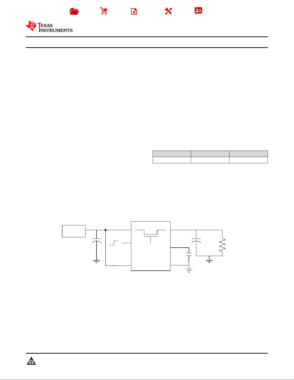
4 Typical Application Schematic
1
An IMPORTANT NOTICE at the end of this data sheet addresses availability, warranty, changes, use in safety-critical applications,
intellectual property matters and other important disclaimers. PRODUCTION DATA.

TPS22967
SLVSC42A –AUGUST 2013–REVISED APRIL 2015
www.ti.com
Table of Contents
1 Features.................................................................. 1
2 Applications ........................................................... 1
3 Description ............................................................. 1
4 Typical Application Schematic............................. 1
5 Revision History..................................................... 2
6 Pin Configuration and Functions......................... 3
7 Specifications......................................................... 4
7.1 Absolute Maximum Ratings ...................................... 4
7.2 ESD Ratings.............................................................. 4
7.3 Recommended Operating Conditions....................... 4
7.4 Thermal Information.................................................. 5
7.5 Electrical Characteristics: V
7.6 Electrical Characteristics: V
7.7 Switching Characteristics.......................................... 7
7.8 Typical Characteristics.............................................. 8
= 5 V ...................... 5
BIAS
= 2.5 V ................... 6
BIAS
8 Detailed Description ............................................ 14
8.1 Overview................................................................. 14
8.2 Functional Block Diagram ....................................... 14
8.3 Feature Description................................................. 14
8.4 Device Functional Modes........................................ 15
9 Application and Implementation........................ 16
9.1 Application Information............................................ 16
9.2 Typical Application ................................................. 17
10 Power Supply Recommendations..................... 19
11 Layout................................................................... 19
11.1 Layout Guidelines ................................................. 19
11.2 Layout Example .................................................... 20
12 Device and Documentation Support................. 20
12.1 Trademarks........................................................... 20
12.2 Electrostatic Discharge Caution............................ 20
12.3 Glossary................................................................ 20
13 Mechanical, Packaging, and Orderable
Information........................................................... 20
5 Revision History
Changes from Original (August 2013) to Revision A Page
• Added Pin Configuration and Functions section, ESD Ratings table, Feature Description section, Device Functional
Modes, Application and Implementation section, Power Supply Recommendations section, Layout section, Device
and Documentation Support section, and Mechanical, Packaging, and Orderable Information section .............................. 1
2 Submit Documentation Feedback Copyright © 2013–2015, Texas Instruments Incorporated
Product Folder Links: TPS22967
TOP VIEW
BOTTOM VIEW
VIN
VIN
ON
VBIAS
VIN
VIN
VBIAS
GND
VOUT
VOUT
CT
GND
VOUT
VOUT
CT
ON
1
2
3
4
8
7
6
5
1
2
3
4
8
7
6
5
www.ti.com
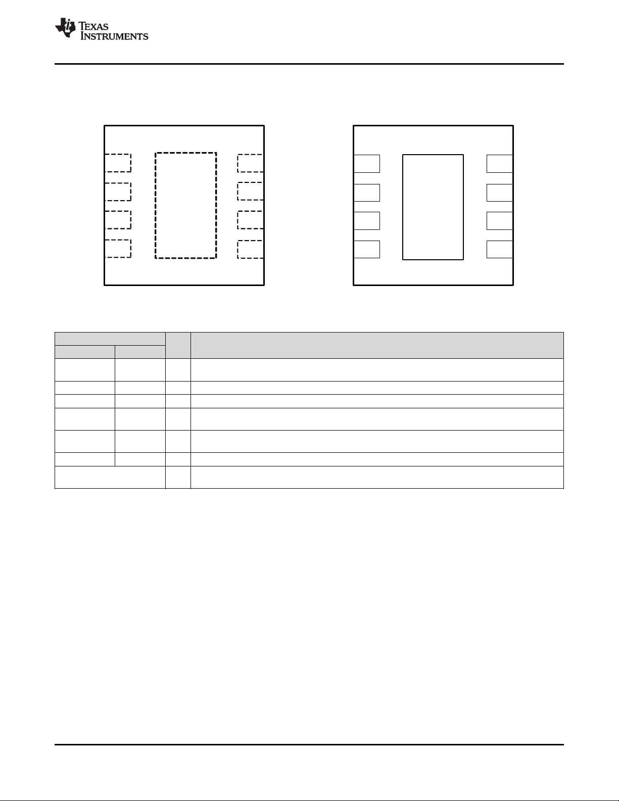
6 Pin Configuration and Functions
DSG Package
8-Pin WSON
Pin Functions
PIN
NAME NO.
CT 6 O
GND 5 – Device ground.
ON 3 I Active high switch control input. Do not leave floating.
VBIAS 4 I
VIN 1, 2 I
VOUT 7, 8 O Switch output.
Thermal Pad –
I/O DESCRIPTION
Switch slew rate control. Can be left floating. See Application and Implementation for more
information.
Bias voltage. Power supply to the device. Recommended voltage range for this pin is 2.5 V to 5.5 V.
See Application Information section for more information.
Switch input. Input capacitor recommended for minimizing VINdip. Recommended voltage range for
this pin for optimal RONperformance is 0.8 V to V
Thermal pad (exposed center pad) to alleviate thermal stress. Tie to GND. See Layout Example for
layout guidelines.
BIAS
TPS22967
SLVSC42A –AUGUST 2013–REVISED APRIL 2015
.
Copyright © 2013–2015, Texas Instruments Incorporated Submit Documentation Feedback 3
Product Folder Links: TPS22967
TPS22967
SLVSC42A –AUGUST 2013–REVISED APRIL 2015
www.ti.com
7 Specifications
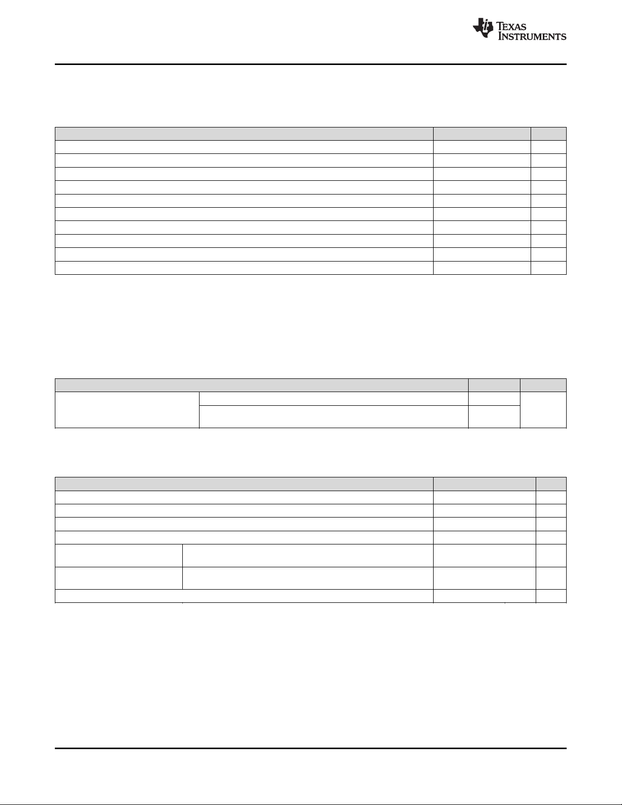
7.1 Absolute Maximum Ratings
Over operating free-air temperature range (unless otherwise noted)
V
V
V
V
I
MAX
I
PLS
T
T
T
T
(1) Stresses beyond those listed under Absolute Maximum Ratings may cause permanent damage to the device. These are stress ratings
(2) All voltage values are with respect to network ground terminal.
(3) In applications where high power dissipation and/or poor package thermal resistance is present, the maximum ambient temperature may
Input voltage –0.3 6 V
IN
Output voltage –0.3 6 V
OUT
Bias voltage –0.3 6 V
BIAS
ON voltage –0.3 6 V
ON
Maximum continuous switch current 4 A
Maximum pulsed switch current, pulse <300 µs, 2% duty cycle 6 A
Operating free-air temperature
A
Maximum junction temperature 125 °C
J
Maximum lead temperature (10-s soldering time) 300 °C
LEAD
Storage temperature –65 150 °C
STG
(3)
only, which do not imply functional operation of the device at these or any other conditions beyond those indicated under Recommended
Operating Conditions. Exposure to absolute-maximum-rated conditions for extended periods may affect device reliability.
have to be derated. Maximum ambient temperature [T
maximum power dissipation of the device in the application [P
in the application (θJA), as given by the following equation: TA
] is dependent on the maximum operating junction temperature [T
A(max)
D(max)
(max)
(1)(2)
MIN MAX UNIT
–40 85 °C
], the
], and the junction-to-ambient thermal resistance of the part/package
= T
J(max)
– (θJA× P
D(max)
).
J(max)
(2)
7.2 ESD Ratings
Human body model (HBM), per ANSI/ESDA/JEDEC JS-001
V
Electrostatic discharge V
(ESD)
Charged device model (CDM), per JEDEC specification JESD22-
(2)
C101
(1) JEDEC document JEP155 states that 500-V HBM allows safe manufacturing with a standard ESD control process.
(2) JEDEC document JEP157 states that 250-V CDM allows safe manufacturing with a standard ESD control process.
(1)
7.3 Recommended Operating Conditions
MIN NOM MAX UNIT
V
V
V
V
V
V
C
(1) Refer to Application Information.
Input voltage 0.8 V
IN
Bias voltage 2.5 5.5 V
BIAS
ON voltage 0 5.5 V
ON
Output voltage V
OUT
High-level input voltage,
IH
ON
Low-level input voltage,
IL
ON
Input capacitor 1
IN
V
= 2.5 V to 5.5 V 1.2 5.5 V
BIAS
V
= 2.5 V to 5.5 V 0 0.5 V
BIAS
(1)
VALUE UNIT
±2000
±1000
BIAS
IN
V
V
µF
4 Submit Documentation Feedback Copyright © 2013–2015, Texas Instruments Incorporated
Product Folder Links: TPS22967

TPS22967
www.ti.com
SLVSC42A –AUGUST 2013–REVISED APRIL 2015
7.4 Thermal Information
TPS22967
THERMAL METRIC
R
θJA
R
θJC(top)
R
θJB
ψ
JT
ψ
JB
R
θJC(bot)
Junction-to-ambient thermal resistance 65.3
Junction-to-case (top) thermal resistance 74.2
Junction-to-board thermal resistance 35.4
Junction-to-top characterization parameter 2.2
Junction-to-board characterization parameter 36
Junction-to-case (bottom) thermal resistance 12.8
(1) For more information about traditional and new thermal metrics, see the IC Package Thermal Metrics application report, SPRA953.
(1)
DSG [WSON] UNIT
8 PINS
°C/W
7.5 Electrical Characteristics: V
BIAS
= 5 V
Unless otherwise noted, the specification in the following table applies over the operating ambient temperature –40°C ≤ T
85°C (Full) and V
POWER SUPPLIES AND CURRENTS
I
IN(VBIAS-ON)VBIAS
I
IN(VBIAS-OFF)VBIAS
I
IN(VIN-OFF)VIN
I
ON
RESISTANCE CHARACTERISTICS
R
ON
R
PD
ON pin input leakage current VON= 5.5 V Full 0.5 µA
ON-state resistance mΩ
Output pulldown resistance VIN= 5.0 V, VON= 0V, I
= 5 V. Typical values are for TA= 25°C.
BIAS
PARAMETER TEST CONDITIONS T
I
= 0,
quiescent current Full 50 75 µA
shutdown current VON= GND, V
OUT
VIN= VON= V
= 5 V
BIAS
= 0 V Full 2 µA
OUT
MIN TYP MAX UNIT
A
VIN= 5 V 0.2 8
off-state supply current Full µA
VON= GND,
V
= 0 V
OUT
VIN= 3.3 V 0.02 3
VIN= 1.8 V 0.01 2
VIN= 0.8 V 0.005 1
25°C 22 33
Full 35
25°C 22 33
Full 35
25°C 22 33
Full 35
25°C 22 33
Full 35
25°C 22 33
Full 35
25°C 22 33
Full 35
I
V
OUT
BIAS
= –200 mA,
= 5 V
VIN= 5 V
VIN= 3.3 V
VIN= 1.8 V
VIN= 1.5 V
VIN= 1.2 V
VIN= 0.8 V
= 15 mA Full 225 300 Ω
OUT
≤
A
Copyright © 2013–2015, Texas Instruments Incorporated Submit Documentation Feedback 5
Product Folder Links: TPS22967

TPS22967
SLVSC42A –AUGUST 2013–REVISED APRIL 2015
www.ti.com
7.6 Electrical Characteristics: V
BIAS
= 2.5 V
Unless otherwise noted, the specification in the following table applies over the operating ambient temperature –40°C ≤ T
85°C (Full) and V
POWER SUPPLIES AND CURRENTS
I
IN(VBIAS-ON)VBIAS
I
IN(VBIAS-OFF)VBIAS
I
IN(VIN-OFF)VIN
I
ON
RESISTANCE CHARACTERISTICS
R
ON
R
PD
ON pin input leakage current VON= 5.5 V Full 0.5 µA
ON-state resistance VIN= 1.5 V mΩ
Output pulldown resistance VIN= 2.5 V, VON= 0 V, I
= 2.5 V. Typical values are for TA= 25°C.
BIAS
PARAMETER TEST CONDITIONS T
I
= 0,
quiescent current Full 20 30 µA
shutdown current VON= GND, V
OUT
VIN= VON= V
= 2.5 V
BIAS
= 0 V Full 2 µA
OUT
MIN TYP MAX UNIT
A
VIN= 2.5 V 0.01 3
off-state supply current Full µA
VON= GND,
V
= 0 V
OUT
VIN= 1.8 V 0.01 2
VIN= 1.2 V 0.005 2
VIN= 0.8 V 0.003 1
25°C 26 38
Full 40
25°C 26 38
Full 40
25°C 25 38
Full 40
25°C 24 38
Full 40
25°C 24 38
Full 40
I
V
OUT
BIAS
= –200 mA,
= 2.5 V
VIN= 2.5 V
VIN= 1.8 V
VIN= 1.2 V
VIN= 0.8 V
= 1 mA Full 275 325 Ω
OUT
≤
A
6 Submit Documentation Feedback Copyright © 2013–2015, Texas Instruments Incorporated
Product Folder Links: TPS22967
+
-
OFF
ON
TPS22967
VIN
VOUT
R
L
C
L
TEST CIRCUIT
GND
(A)
GND
t
R
t
F
t
ON
t
OFF
90% 90%
10% 10%
tON/t
OFF
WAVEFORMS
(A) Rise and fall times of the control signal is 100ns.
V
ON
V
OUT
V
OUT
ON
GND
50% 50%
50% 50%
CIN= 1µF
VBIAS
CT
t
D
10%
www.ti.com
7.7 Switching Characteristics
PARAMETER TEST CONDITIONS MIN TYP MAX UNIT
VIN= VON= V
t
t
t
t
t
ON
OFF
R
F
D
Turnon time 1325
Turnoff time 10
V
V
ON delay time 500
VIN= 0.8 V, VON= V
t
t
t
t
t
ON
OFF
R
F
D
Turnon time 600
Turnoff time 80
V
V
ON delay time 460
VIN= 2.5 V, VON= 5 V, V
t
t
t
t
t
ON
OFF
R
F
D
Turnon time 2200
Turnoff time 9
V
V
ON delay time 1075
VIN= 0.8 V, VON= 5 V, V
t
t
t
t
t
ON
OFF
R
F
D
Turn-on time 1450
Turn-off time 60
V
V
ON delay time 1010
= 5 V, TA= 25ºC (UNLESS OTHERWISE NOTED)
BIAS
rise time RL= 10 Ω, CL= 0.1 µF, CT= 1000 pF 1625 µs
OUT
fall time 3.5
OUT
= 5 V, TA= 25ºC (UNLESS OTHERWISE NOTED)
BIAS
rise time RL= 10 Ω, CL= 0.1 µF, CT= 1000 pF 300 µs
OUT
fall time 5.5
OUT
= 2.5 V, TA= 25ºC (UNLESS OTHERWISE NOTED)
BIAS
rise time RL= 10 Ω, CL= 0.1 µF, CT= 1000 pF 2275 µs
OUT
fall time 3.1
OUT
= 2.5 V, TA= 25ºC (UNLESS OTHERWISE NOTED)
BIAS
rise time RL= 10 Ω, CL= 0.1 µF, CT= 1000 pF 875 µs
OUT
fall time 5.5
OUT
TPS22967
SLVSC42A –AUGUST 2013–REVISED APRIL 2015
Copyright © 2013–2015, Texas Instruments Incorporated Submit Documentation Feedback 7
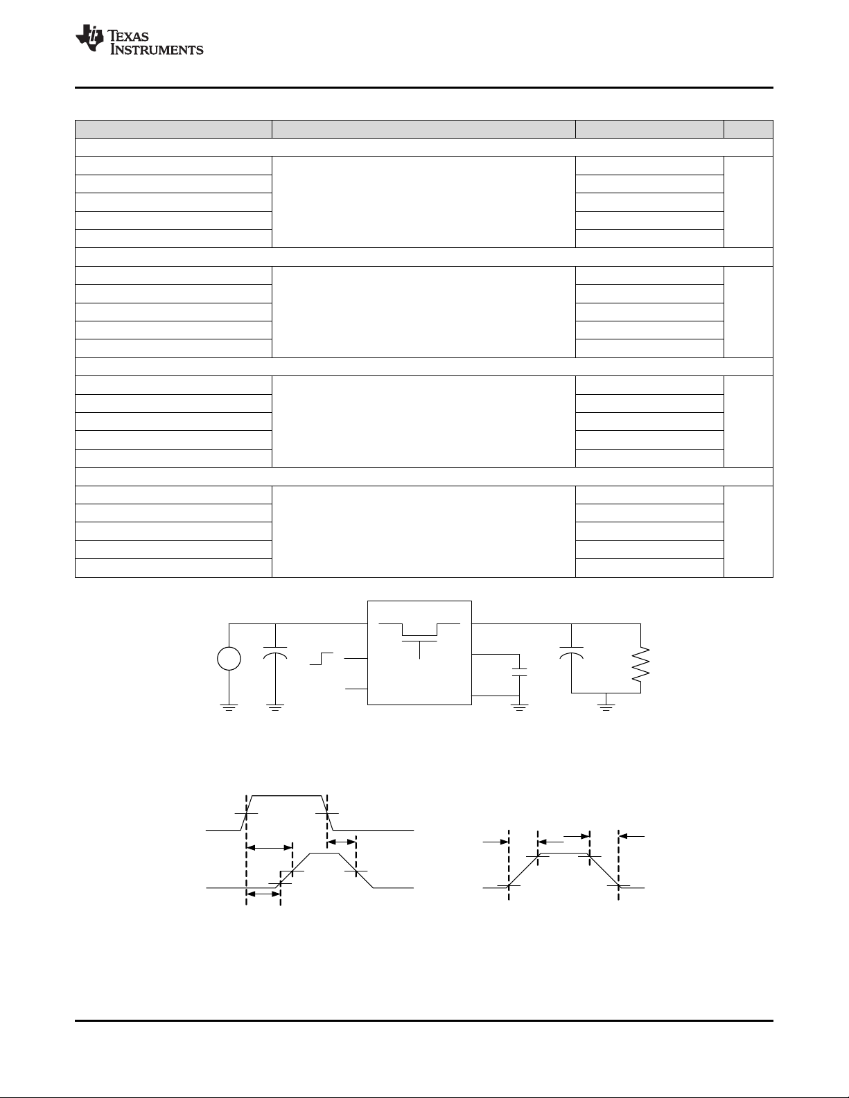
Figure 1. Test Circuit and Timing Waveforms
Product Folder Links: TPS22967
16
16.5
17
17.5
18
18.5
19
19.5
20
20.5
21
21.5
22
22.5
23
23.5
24
24.5
25
25.5
26
26.5
27
27.5
28
-40 -15 10 35 60 85
R
ON
(m)
Temperature (C)
VIN = 0.8V
VIN = 1.05V
VIN = 1.2V
VIN = 1.5V
VIN = 1.8V
VIN = 2.5V
VIN = 3.3V
VIN = 3.6V
VIN = 4.2V
VIN =5V
VIN = 5.5V
C002
VBIAS=5.5V, I
OUT
= -200mA
17
18
19
20
21
22
23
24
25
26
27
28
29
30
31
32
33
34
35
0.8 1.2 1.6 2 2.4
R
ON
(m)
VIN (V)
-40C
25C
85C
70C
C002
VBIAS=2.5V, I
OUT
= -200mA
18
19
20
21
22
23
24
25
26
27
28
29
30
31
32
33
-40 -15 10 35 60 85
R
ON
(m)
Temperature (ºC)
VIN = 0.8V
VIN = 1.05V
VIN = 1.2V
VIN = 1.5V
VIN = 1.8V
VIN =2.5V
C002
VBIAS=2.5V, I
OUT
=-200mA
TPS22967
SLVSC42A –AUGUST 2013–REVISED APRIL 2015
7.8 Typical Characteristics
www.ti.com
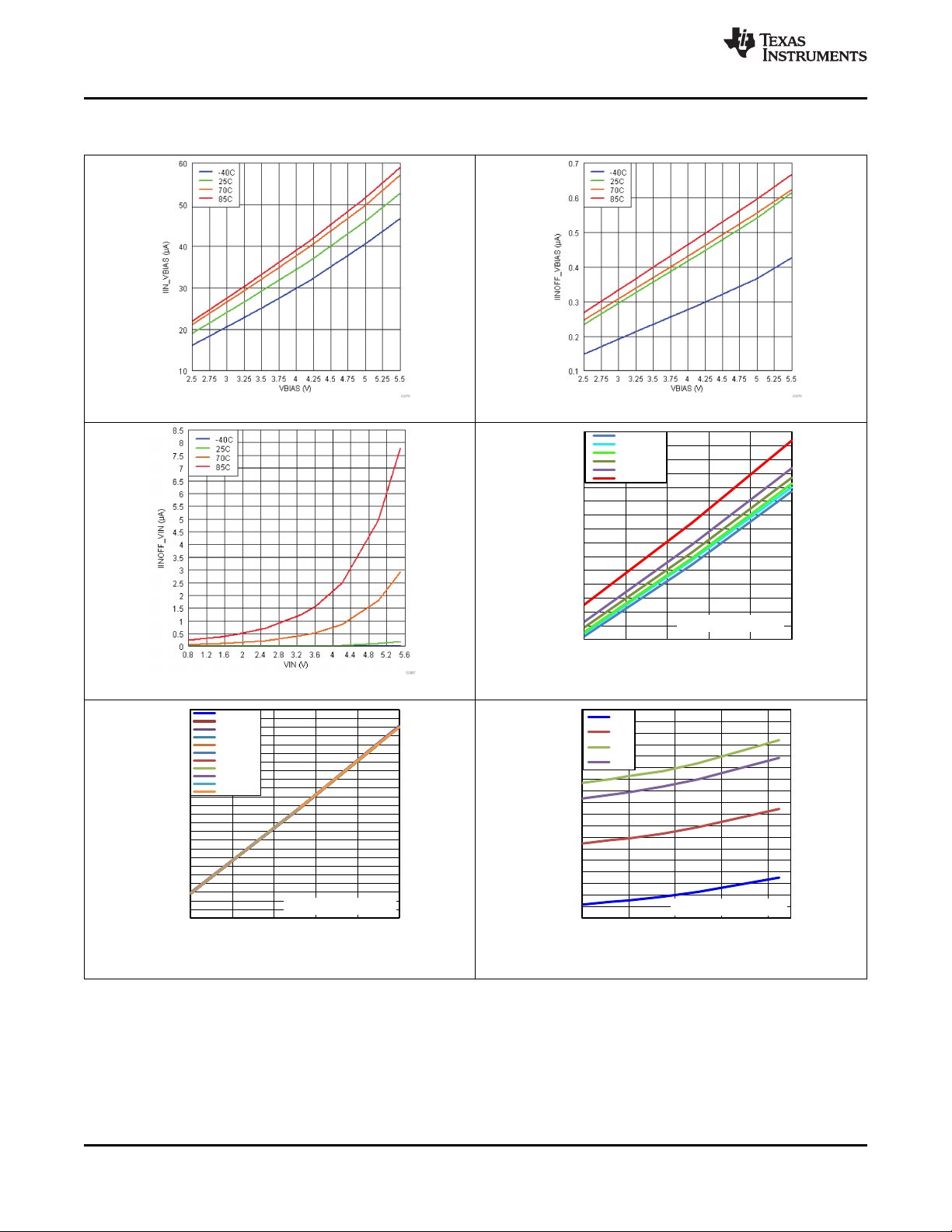
Figure 2. V
vs Quiescent Current Figure 3. V
BIAS
Figure 4. VINvs Off-State VIN Current
vs Shutdown Current
BIAS
Figure 5. Temperature vs RON(V
BIAS
= 2.5 V)
Figure 6. Temperature vs RON(V
8 Submit Documentation Feedback Copyright © 2013–2015, Texas Instruments Incorporated
= 5.5 V) Figure 7. VINvs RON(V
BIAS
Product Folder Links: TPS22967
BIAS
= 2.5 V)
21
22
23
24
25
26
27
0.8 1.2 1.6 2 2.4 2.8 3.2 3.6 4 4.4 4.8 5.2 5.6
R
ON
(mΩ)
VIN (V)
VBIAS = 2.5V
VBIAS = 3.3V
VBIAS = 3.6V
VBIAS = 4.2V
VBIAS = 5V
VBIAS = 5.5V
C002
Temperature=25C, I
OUT
= -200mA
15
17
19
21
23
25
27
29
31
33
0.8 1.2 1.6 2 2.4 2.8 3.2 3.6 4 4.4 4.8 5.2 5.6
R
ON
(m)
VIN (V)
-40C
25C
70C
85C
C002
VBIAS=5.5V, I
OUT
= -200mA
www.ti.com
Typical Characteristics (continued)
TPS22967
SLVSC42A –AUGUST 2013–REVISED APRIL 2015
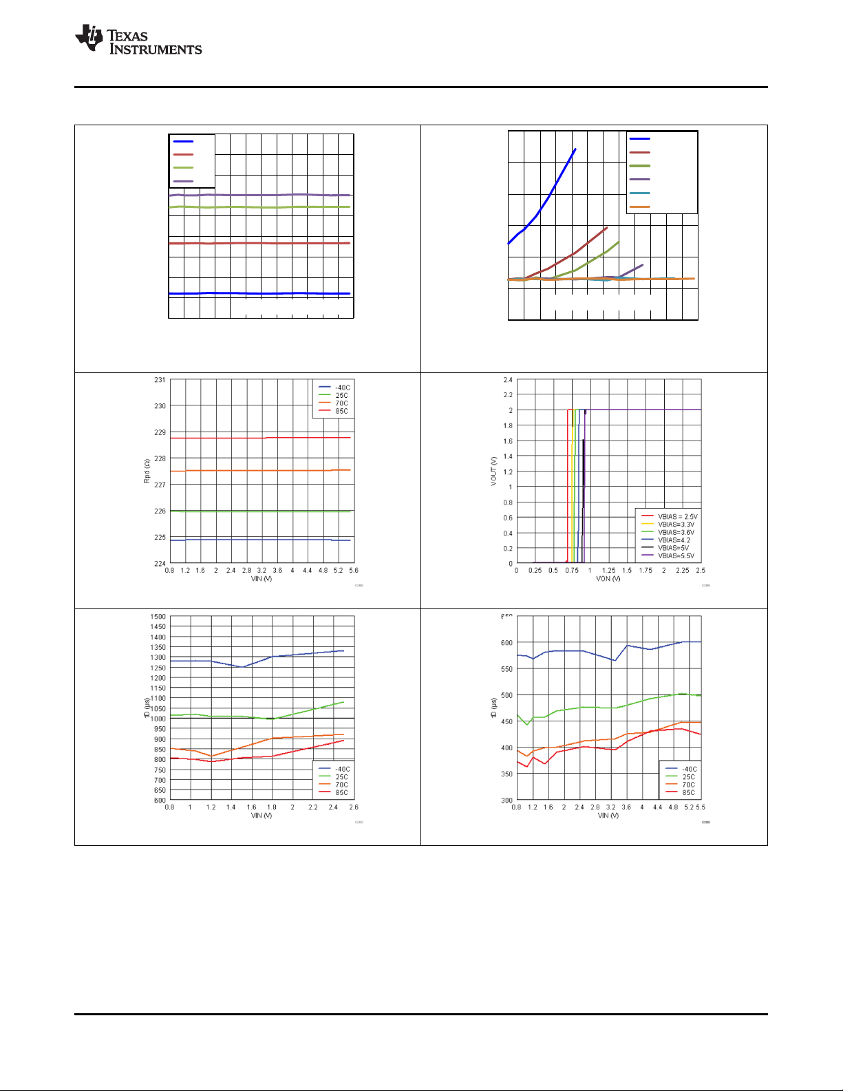
Figure 8. VINvs RON(V
Figure 10. VIN vs RPD(V
= 5.5 V)
BIAS
= 5.5 V) Figure 11. VONvs V
BIAS
Figure 9. VINvs RON(TA= 25°C)
OUT(TA
= 25°C)
Figure 12. VINvs tD(V
Copyright © 2013–2015, Texas Instruments Incorporated Submit Documentation Feedback 9
= 2.5 V, CT = 1 nF) Figure 13. VINvs tD(V
BIAS
= 5.5 V, CT = 1 nF)
BIAS
Product Folder Links: TPS22967

TPS22967
SLVSC42A –AUGUST 2013–REVISED APRIL 2015
Typical Characteristics (continued)
www.ti.com
Figure 14. VINvs tF(V
Figure 16. VINvs t
OFF(VBIAS
= 2.5 V, CT = 1 nF) Figure 15. VINvs tF(V
BIAS
= 2.5 V, CT = 1 nF) Figure 17. VINvs t
BIAS
OFF(VBIAS
= 5.5 V, CT = 1 nF)
= 5.5 V, CT = 1 nF)
Figure 18. VINvs tON(V
= 2.5 V, CT = 1 nF) Figure 19. VINvs tON(V
BIAS
= 5.5 V, CT = 1 nF)
BIAS
10 Submit Documentation Feedback Copyright © 2013–2015, Texas Instruments Incorporated
Product Folder Links: TPS22967
www.ti.com
Typical Characteristics (continued)
TPS22967
SLVSC42A –AUGUST 2013–REVISED APRIL 2015
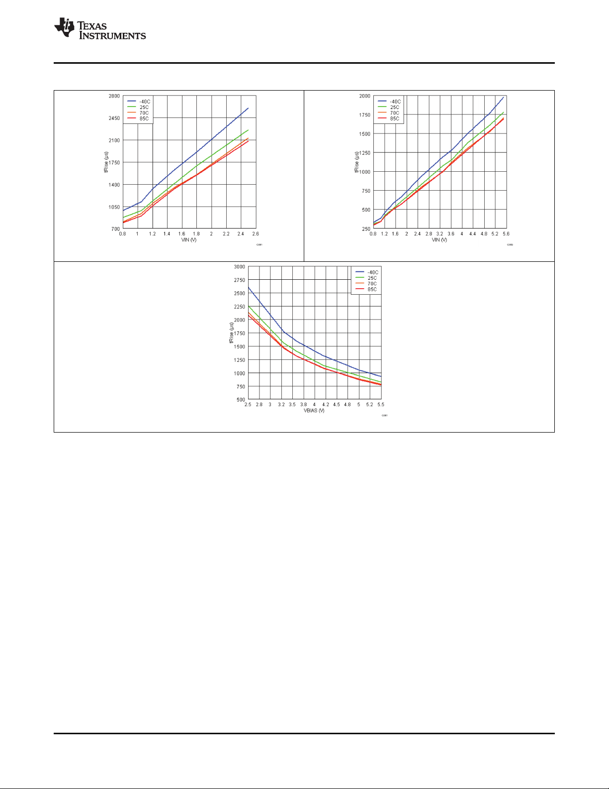
Figure 20. VINvs tR(V
= 2.5 V, CT = 1 nF) Figure 21. VINvs tR(V
BIAS
Figure 22. V
vs tR(VIN= 2.5 V, CT = 1 nF)
BIAS
= 5.5 V, CT = 1 nF)
BIAS
Copyright © 2013–2015, Texas Instruments Incorporated Submit Documentation Feedback 11
Product Folder Links: TPS22967

TPS22967
SLVSC42A –AUGUST 2013–REVISED APRIL 2015
7.8.1 Typical AC Scope Captures at TA= 25ºC, CT = 1 nF
Figure 23. Turnon Response Time Figure 24. Turnon Response Time
(VIN= 0.8 V, V
= 2.5 V, CIN= 1 µF, CL= 0.1 µF, (VIN= 0.8 V, V
BIAS
RL= 10 Ω) CH1: VOUT, CH2: ON
CH1: VOUT, CH2: ON
= 5 V, CIN= 1 µF, CL= 0.1 µF, RL= 10 Ω)
BIAS
www.ti.com
Figure 25. Turnon Response Time
(VIN= 2.5 V, V
= 2.5 V, CIN= 1 µF, CL= 0.1 µF,
BIAS
RL= 10 Ω)
(VIN= 5 V, V
Figure 26. Turnon Response Time
= 5 V, CIN= 1 µF, CL= 0.1 µF, RL= 10 Ω)
BIAS
CH1: VOUT, CH2: ON
CH1: VOUT, CH2: ON
Figure 27. Turnoff Response Time Figure 28. Turnoff Response Time
(VIN= 0.8 V, V
= 2.5 V, CIN= 1 µF, CL= 0.1 µF, (VIN= 0.8 V, V
BIAS
= 5 V, CIN= 1 µF, CL= 0.1 µF, RL= 10 Ω)
BIAS
RL= 10 Ω) CH1: VOUT, CH2: ON
CH1: VOUT, CH2: ON
12 Submit Documentation Feedback Copyright © 2013–2015, Texas Instruments Incorporated
Product Folder Links: TPS22967

www.ti.com
Typical AC Scope Captures at TA= 25ºC, CT = 1 nF (continued)
Figure 29. Turnoff Response Time Figure 30. Turnoff Response Time
(VIN= 2.5 V, V
= 2.5 V, CIN= 1 µF, CL= 0.1 µF, (VIN= 5 V, V
BIAS
RL= 10 Ω) CH1: VOUT, CH2: ON
CH1: VOUT, CH2: ON
TPS22967
SLVSC42A –AUGUST 2013–REVISED APRIL 2015
= 5 V, CIN= 1 µF, CL= 0.1 µF, RL= 10 Ω)
BIAS
Copyright © 2013–2015, Texas Instruments Incorporated Submit Documentation Feedback 13
Product Folder Links: TPS22967

Charge
Pump
Control
Logic
VIN
ON
VOUT
GND
CT
VBIAS
TPS22967
SLVSC42A –AUGUST 2013–REVISED APRIL 2015
www.ti.com
8 Detailed Description
8.1 Overview
The TPS22967 device is a single-channel, 4-A load switch in an 8-pin WSON package. To reduce the voltage
drop in high current rails, the device implements an ultra-low resistance N-channel MOSFET. The device has a
programmable slew rate for applications that require specific rise time.
The device has very low leakage current during off state. This prevents downstream circuits from pulling high
standby current from the supply. Integrated control logic, driver, power supply, and output discharge FET
eliminates the need for any external components, which reduces solution size and bill of materials (BOM) count.
8.2 Functional Block Diagram
8.3 Feature Description
This section describes the integrated features for the TPS22967.
8.3.1 ON/OFF Control
The ON pin controls the state of the switch. Asserting ON high enables the switch. ON is active high and has a
low threshold, making it capable of interfacing with low-voltage signals. The ON pin is compatible with standard
GPIO logic thresholds. It can be used with any microcontroller with 1.2 V or higher GPIO voltage. This pin cannot
be left floating and must be driven either high or low for proper functionality.
14 Submit Documentation Feedback Copyright © 2013–2015, Texas Instruments Incorporated
Product Folder Links: TPS22967

SR 0.39 CT 13.4= ´ +
TPS22967
www.ti.com
SLVSC42A –AUGUST 2013–REVISED APRIL 2015
Feature Description (continued)
8.3.2 Adjustable Rise Time
A capacitor to GND on the CT pin sets the VOUT slew rate. The voltage on the CT pin can be as high as 12 V.
Therefore, the minimum voltage rating for the CT capacitor must be 25 V for optimal performance. An
approximate formula for the relationship between CT and slew rate is (Equation 1 accounts for 10% to 90%
measurement on V
pF):
where
• SR = slew rate (in µs/V).
• CT = the capacitance value on the CT pin (in pF).
• The units for the constant 13.4 is in µs/V. The units for the constant 0.39 are in µs/(V × pF). (1)
Rise time can be calculated by multiplying the input voltage by the slew rate. Table 1 contains rise time values
measured on a typical device. Rise times shown below are only valid for the power-up sequence where VINand
V
are already in steady state condition, and the ON pin is asserted high.
BIAS
CTx (pF)
0 127 93 62 55 51 46 42
220 475 314 188 162 141 125 103
470 939 637 359 304 255 218 188
1000 1869 1229 684 567 476 414 344
2200 4020 2614 1469 1211 1024 876 681
4700 8690 5746 3167 2703 2139 1877 1568
10000 18360 12550 6849 5836 4782 4089 3449
and does NOT apply for CT = 0 pF. Use Table 1 to determine rise times for when CT = 0
OUT
Table 1. Rise Times On a Typical Device
RISE TIME (µs) 10% - 90%, CL= 0.1 µF, CIN= 1 µF, RL= 10 Ω
TYPICAL VALUES at 25°C, 25 V X7R 10% CERAMIC CAPACITOR
5 V 3.3 V 1.8 V 1.5 V 1.2 V 1.05 V 0.8 V
8.3.3 Quick Output Discharge
The TPS22967 includes a Quick Output Discharge (QOD) feature. When the switch is disabled, a discharge
resistor is connected between VOUT and GND. This resistor has a typical value of 225 Ω and prevents the
output from floating while the switch is disabled.
8.4 Device Functional Modes
Table 2 describes the functional state of the load switch as determined by the ON pin.
Table 2. Functional Table
ON VIN to VOUT VOUT to GND
L Off On
H On Off
Copyright © 2013–2015, Texas Instruments Incorporated Submit Documentation Feedback 15
Product Folder Links: TPS22967
20
25
30
35
40
45
50
0.8 1.2 1.6 2 2.4 2.8 3.2 3.6 4 4.4 4.8 5.2 5.6
R
ON
(m)
VIN (V)
VBIAS = 2.5V
VBIAS = 3.3V
VBIAS = 3.6V
VBIAS = 4.2V
VBIAS = 5V
VBIAS = 5.5V
C017
Temperature=25C,
I
OUT
=-200mA
TPS22967
SLVSC42A –AUGUST 2013–REVISED APRIL 2015
www.ti.com
9 Application and Implementation
NOTE
Information in the following applications sections is not part of the TI component
specification, and TI does not warrant its accuracy or completeness. TI’s customers are
responsible for determining suitability of components for their purposes. Customers should
validate and test their design implementation to confirm system functionality.
9.1 Application Information
This section describes design considerations for the TPS22967 which can vary depending on the specific
application.
9.1.1 Input Capacitor (Optional)
To limit the voltage drop on the input supply caused by transient inrush currents when the switch turns on into a
discharged load capacitor or short circuit, a capacitor must be placed between VIN and GND. A 1-µF ceramic
capacitor, CIN, placed close to the pins, is usually sufficient. Higher values of CINcan be used to further reduce
the voltage drop during high-current applications. When switching heavy loads, TI recommends having an input
capacitor about 10 times higher than the output capacitor to avoid excessive voltage drop.
9.1.2 Output Capacitor (Optional)
Because of the integrated body diode in the NMOS switch, a CINgreater than CLis highly recommended. A C
greater than CINcan cause V
flow through the body diode from VOUT to VIN. A CINto CLratio of 10 to 1 is recommended for minimizing V
dip caused by inrush currents during start-up; however, a 10-to-1 ratio for capacitance is not required for proper
functionality of the device. A ratio smaller than 10 to 1 (such as 1 to 1) could cause slightly more VINdip upon
turnon due to inrush currents. This can be mitigated by increasing the capacitance on the CT pin for a longer rise
time (see below).
to exceed VINwhen the system supply is removed. This could result in current
OUT
L
IN
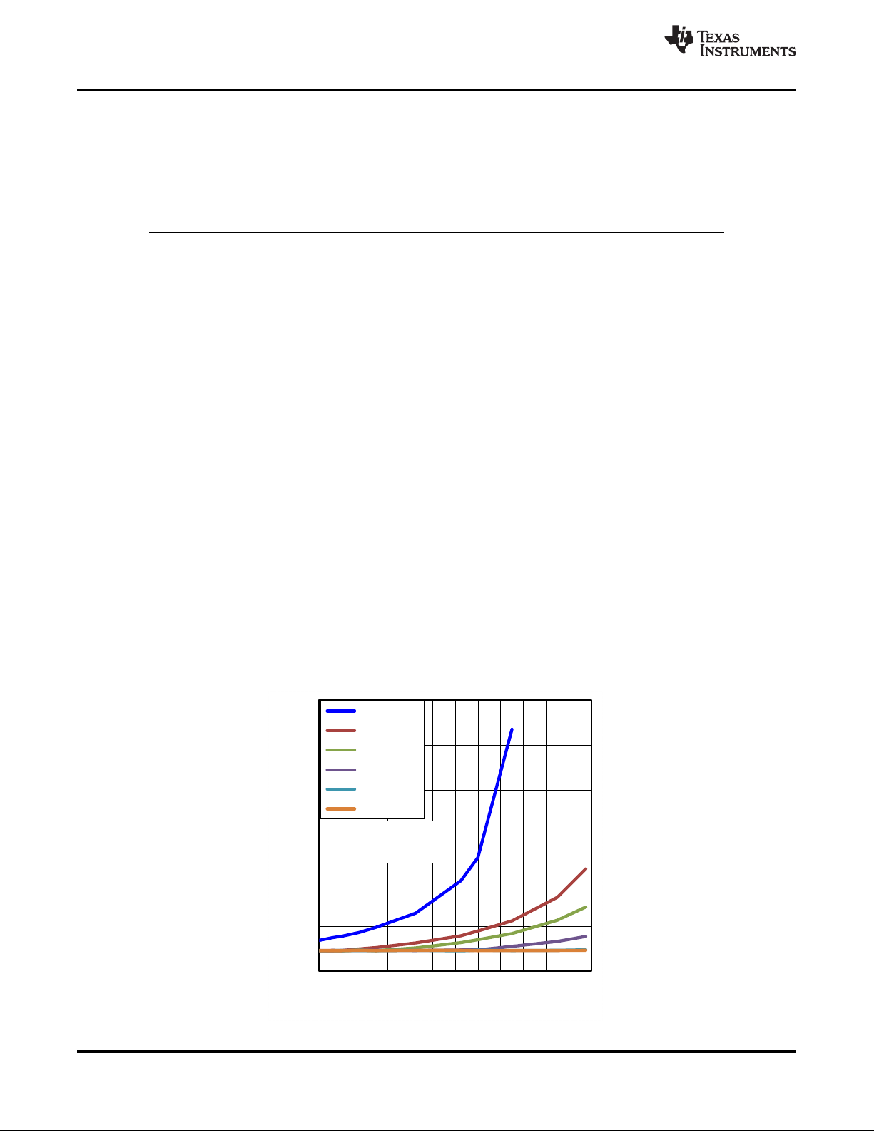
9.1.3 VINand V
For optimal RONperformance, make sure VIN≤ V
Voltage Range
BIAS
. The device will still be functional if VIN> V
BIAS
exhibit RONgreater than what is listed in the Electrical Characteristics: V
example of a typical device. Notice the increasing RONas VINexceeds V
BIAS
voltage rating for VIN and VBIAS.
but it will
= 5 V table. See Figure 31 for an
BIAS
BIAS
voltage. Never exceed the maximum
16 Submit Documentation Feedback Copyright © 2013–2015, Texas Instruments Incorporated
Figure 31. RONvs VIN(VIN> V
Product Folder Links: TPS22967
BIAS
)
Power
Supply
OFF
ON
TPS22967
VIN
VOUT
R
L
C
L
GND
ON
CT
C
IN
VBIAS
GND
0
1
2
3
4
5
-40 -15 10 35 60 85
Continuous Current (A)
Ambient Temperature (ºC)
100% On time
90% On time
70% On time
50% On time
30% On time
C002
VBIAS=5.0V
TPS22967
www.ti.com
SLVSC42A –AUGUST 2013–REVISED APRIL 2015
Application Information (continued)
9.1.4 Safe Operating Area (SOA)
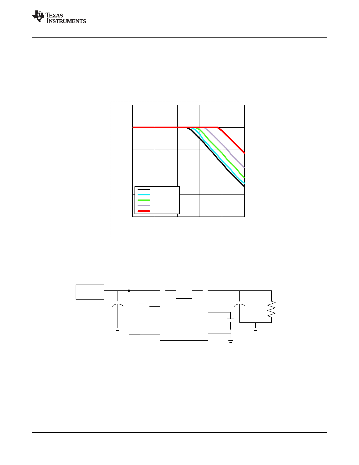
The SOA curves show the continuous current carrying capability of the device versus ambient temperature (TA)
to ensure reliable operation over 70,000 hours of device lifetime. The different curves represent the percentage
On time over device lifetime and can be used as a reference to understand the current carrying capability of
TPS22967 under different use cases. TI recommends maintaining continuous current at or below the SOA
curves shown in Figure 32.
On time is the duration of time that the device is enabled (ON ≥ VIH) over 70,000 hour lifetime.
9.2 Typical Application
Copyright © 2013–2015, Texas Instruments Incorporated Submit Documentation Feedback 17
Figure 32. Safe Operating Area
Figure 33. Typical Application Schematic
Product Folder Links: TPS22967
TPS22967
SLVSC42A –AUGUST 2013–REVISED APRIL 2015
www.ti.com
Typical Application (continued)
9.2.1 Design Requirements
For this design example, use the parameters listed in Table 3 as the input parameters.
Table 3. Design Parameters
DESIGN PARAMETER EXAMPLE VALUE
V
IN
V
BIAS
C
L
Maximum Acceptable Inrush Current 400 mA
9.2.2 Detailed Design Procedure
9.2.2.1 Inrush Current
When the switch is enabled, the output capacitors must be charged up from 0 V to the set value (3.3 V in this
example). This charge arrives in the form of inrush current. Inrush current can be calculated using Equation 2:
Inrush Current = C × dV/dt
where
• C = output capacitance.
• dV = output voltage.
• dt = rise time. (2)
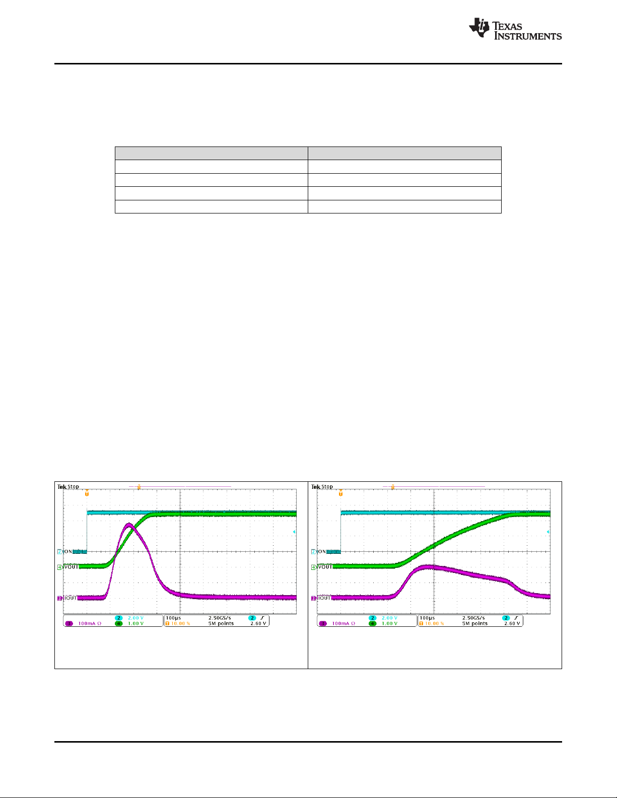
The TPS22967 offers adjustable rise time for VOUT. This feature lets the user control the inrush current during
turnon. The appropriate rise time can be calculated using the design requirements and the inrush current
equation.
400 mA = 22 μ F × 3.3 V/dt (3)
dt = 181.5 μs (4)
To ensure an inrush current of less than 400 mA, choose a CT value that will yield a rise time of more than 181.5
μs. See Application Curves for an example of how the CT capacitor can be used to reduce inrush current.
3.3 V
5 V
22 μF
9.2.3 Application Curves
V
= 5 V VIN= 3.3 V CL= 22 μF V
BIAS
Figure 34. Inrush Current With CT = 0 pF Figure 35. Inrush Current with CT = 220 pF
18 Submit Documentation Feedback Copyright © 2013–2015, Texas Instruments Incorporated
Product Folder Links: TPS22967
= 5 V VIN= 3.3 V CL= 22 μF
BIAS

J(max) A
D(max)
JA
T T
-
=
θ
TPS22967
www.ti.com
SLVSC42A –AUGUST 2013–REVISED APRIL 2015
10 Power Supply Recommendations
The device is designed to operate from a VBIAS range of 2.5 V to 5.5 V and a VIN range of 0.8 V to 5.5 V. The
power supply must be well regulated and placed as close to the device terminals as possible. It must be able to
withstand all transient and load current steps. In most situations, using an input capacitance of 1 μF is sufficient
to prevent the supply voltage from dipping when the switch is turned on. In cases where the power supply is slow
to respond to a large transient current or large load current step, additional bulk capacitance may be required on
the input.
The requirements for larger input capacitance can be mitigated by adding additional capacitance to the CT pin.
This additional capacitance causes the load switch to turn on more slowly. Not only will this reduce transient
inrush current, but it will also give the power supply more time to respond to the load current step.
11 Layout
11.1 Layout Guidelines
For best performance, all traces must be as short as possible. To be most effective, the input and output
capacitors must be placed close to the device to minimize the effects that parasitic trace inductances may have
on normal operation. Using wide traces for VIN, VOUT, and GND helps minimize the parasitic electrical effects
along with minimizing the case to ambient thermal impedance.
The maximum IC junction temperature must be restricted to 125°C under normal operating conditions. To
calculate the maximum allowable dissipation, P
Equation 5 as a guideline:
for a given output current and ambient temperature, use
D(max)
where
• P
• T
• TA= ambient temperature of the device.
• ΘJA= junction to air thermal impedance. See Thermal Information. This parameter is highly dependent upon
= maximum allowable power dissipation.
D(max)
= maximum allowable junction temperature (125°C for the TPS22967).
J(max)
board layout. (5)
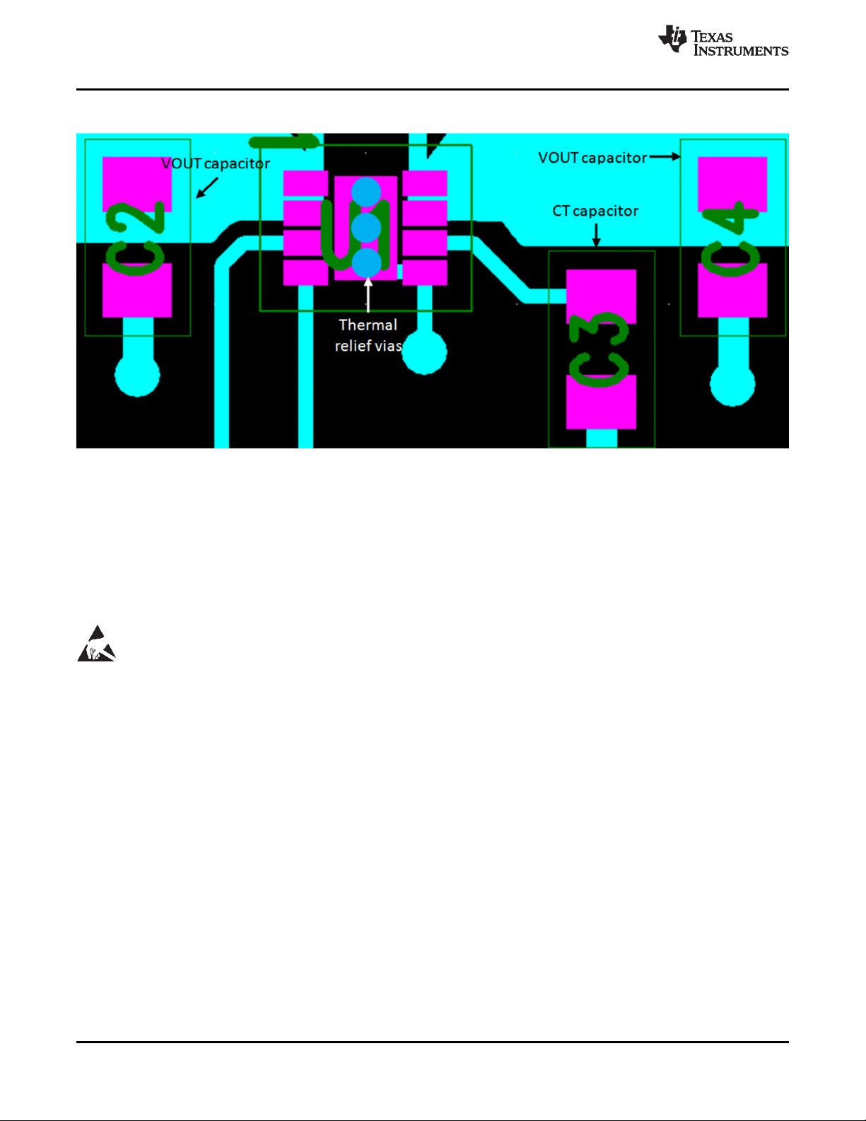
Figure 36 shows an example of a layout. Notice the thermal vias under the exposed thermal pad of the device.
This allows for thermal diffusion away from the device.
Copyright © 2013–2015, Texas Instruments Incorporated Submit Documentation Feedback 19
Product Folder Links: TPS22967
TPS22967
SLVSC42A –AUGUST 2013–REVISED APRIL 2015
11.2 Layout Example
www.ti.com
Figure 36. Layout Example
12 Device and Documentation Support
12.1 Trademarks
Ultrabooks is a trademark of Intel.
All other trademarks are the property of their respective owners.
12.2 Electrostatic Discharge Caution
These devices have limited built-in ESD protection. The leads should be shorted together or the device placed in conductive foam
during storage or handling to prevent electrostatic damage to the MOS gates.
12.3 Glossary
SLYZ022 — TI Glossary.
This glossary lists and explains terms, acronyms, and definitions.
13 Mechanical, Packaging, and Orderable Information
The following pages include mechanical, packaging, and orderable information. This information is the most
current data available for the designated devices. This data is subject to change without notice and revision of
this document. For browser-based versions of this data sheet, refer to the left-hand navigation.
20 Submit Documentation Feedback Copyright © 2013–2015, Texas Instruments Incorporated
Product Folder Links: TPS22967
PACKAGE OPTION ADDENDUM
www.ti.com
21-Feb-2015
PACKAGING INFORMATION
Orderable Device Status
TPS22967DSGR ACTIVE WSON DSG 8 3000 Green (RoHS
TPS22967DSGT ACTIVE WSON DSG 8 250 Green (RoHS
(1)
The marketing status values are defined as follows:
ACTIVE: Product device recommended for new designs.
LIFEBUY: TI has announced that the device will be discontinued, and a lifetime-buy period is in effect.
NRND: Not recommended for new designs. Device is in production to support existing customers, but TI does not recommend using this part in a new design.
PREVIEW: Device has been announced but is not in production. Samples may or may not be available.
OBSOLETE: TI has discontinued the production of the device.
Package Type Package
(1)
Drawing
Pins Package
Qty
Eco Plan
(2)
& no Sb/Br)
& no Sb/Br)
Lead/Ball Finish
(6)
CU NIPDAU Level-2-260C-1 YEAR -40 to 85 ZTU
CU NIPDAU Level-2-260C-1 YEAR -40 to 85 ZTU
MSL Peak Temp
(3)
Op Temp (°C) Device Marking
(4/5)
(2)
Eco Plan - The planned eco-friendly classification: Pb-Free (RoHS), Pb-Free (RoHS Exempt), or Green (RoHS & no Sb/Br) - please check http://www.ti.com/productcontent for the latest availability
information and additional product content details.
TBD: The Pb-Free/Green conversion plan has not been defined.
Pb-Free (RoHS): TI's terms "Lead-Free" or "Pb-Free" mean semiconductor products that are compatible with the current RoHS requirements for all 6 substances, including the requirement that
lead not exceed 0.1% by weight in homogeneous materials. Where designed to be soldered at high temperatures, TI Pb-Free products are suitable for use in specified lead-free processes.
Pb-Free (RoHS Exempt): This component has a RoHS exemption for either 1) lead-based flip-chip solder bumps used between the die and package, or 2) lead-based die adhesive used between
the die and leadframe. The component is otherwise considered Pb-Free (RoHS compatible) as defined above.
Green (RoHS & no Sb/Br): TI defines "Green" to mean Pb-Free (RoHS compatible), and free of Bromine (Br) and Antimony (Sb) based flame retardants (Br or Sb do not exceed 0.1% by weight
in homogeneous material)
(3)
MSL, Peak Temp. - The Moisture Sensitivity Level rating according to the JEDEC industry standard classifications, and peak solder temperature.
(4)
There may be additional marking, which relates to the logo, the lot trace code information, or the environmental category on the device.
(5)
Multiple Device Markings will be inside parentheses. Only one Device Marking contained in parentheses and separated by a "~" will appear on a device. If a line is indented then it is a continuation
of the previous line and the two combined represent the entire Device Marking for that device.
(6)
Lead/Ball Finish - Orderable Devices may have multiple material finish options. Finish options are separated by a vertical ruled line. Lead/Ball Finish values may wrap to two lines if the finish
value exceeds the maximum column width.
Important Information and Disclaimer:The information provided on this page represents TI's knowledge and belief as of the date that it is provided. TI bases its knowledge and belief on information
provided by third parties, and makes no representation or warranty as to the accuracy of such information. Efforts are underway to better integrate information from third parties. TI has taken and
continues to take reasonable steps to provide representative and accurate information but may not have conducted destructive testing or chemical analysis on incoming materials and chemicals.
TI and TI suppliers consider certain information to be proprietary, and thus CAS numbers and other limited information may not be available for release.
Samples
Addendum-Page 1

PACKAGE OPTION ADDENDUM
www.ti.com
In no event shall TI's liability arising out of such information exceed the total purchase price of the TI part(s) at issue in this document sold by TI to Customer on an annual basis.
21-Feb-2015
Addendum-Page 2
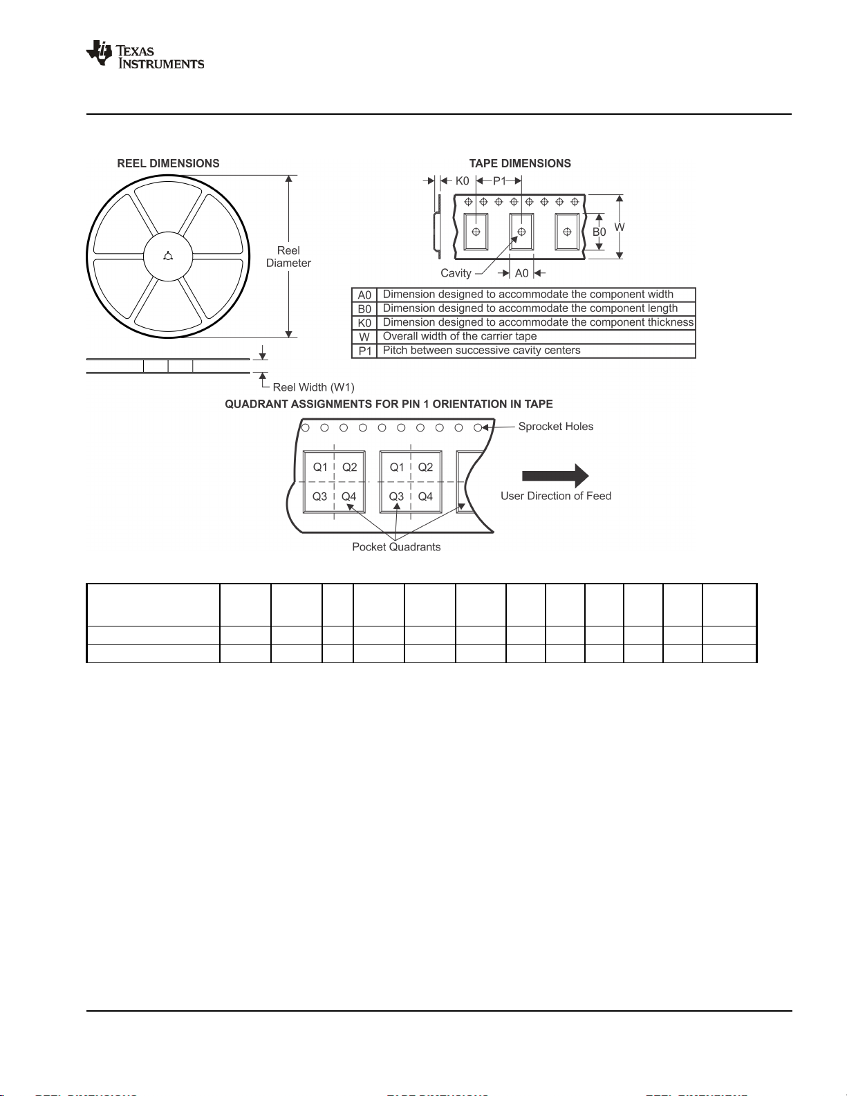
PACKAGE MATERIALS INFORMATION
www.ti.com 10-Jul-2015
TAPE AND REEL INFORMATION
*All dimensions are nominal
Device Package
TPS22967DSGR WSON DSG 8 3000 180.0 8.4 2.3 2.3 1.15 4.0 8.0 Q2
TPS22967DSGT WSON DSG 8 250 180.0 8.4 2.3 2.3 1.15 4.0 8.0 Q2
Type
Package
Drawing
Pins SPQ Reel
Diameter
(mm)
Reel
Width
W1 (mm)
A0
(mm)B0(mm)K0(mm)P1(mm)W(mm)
Pin1
Quadrant
Pack Materials-Page 1
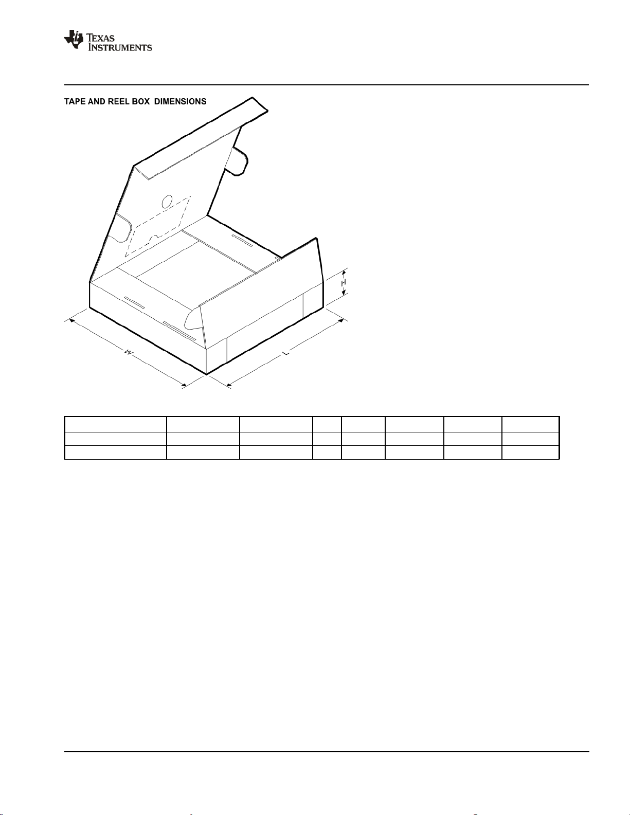
PACKAGE MATERIALS INFORMATION
www.ti.com 10-Jul-2015
*All dimensions are nominal
Device Package Type Package Drawing Pins SPQ Length (mm) Width (mm) Height (mm)
TPS22967DSGR WSON DSG 8 3000 210.0 185.0 35.0
TPS22967DSGT WSON DSG 8 250 210.0 185.0 35.0
Pack Materials-Page 2


IMPORTANT NOTICE
Texas Instruments Incorporated and its subsidiaries (TI) reserve the right to make corrections, enhancements, improvements and other
changes to its semiconductor products and services per JESD46, latest issue, and to discontinue any product or service per JESD48, latest
issue. Buyers should obtain the latest relevant information before placing orders and should verify that such information is current and
complete. All semiconductor products (also referred to herein as “components”) are sold subject to TI’s terms and conditions of sale
supplied at the time of order acknowledgment.
TI warrants performance of its components to the specifications applicable at the time of sale, in accordance with the warranty in TI’s terms
and conditions of sale of semiconductor products. Testing and other quality control techniques are used to the extent TI deems necessary
to support this warranty. Except where mandated by applicable law, testing of all parameters of each component is not necessarily
performed.
TI assumes no liability for applications assistance or the design of Buyers’ products. Buyers are responsible for their products and
applications using TI components. To minimize the risks associated with Buyers’ products and applications, Buyers should provide
adequate design and operating safeguards.
TI does not warrant or represent that any license, either express or implied, is granted under any patent right, copyright, mask work right, or
other intellectual property right relating to any combination, machine, or process in which TI components or services are used. Information
published by TI regarding third-party products or services does not constitute a license to use such products or services or a warranty or
endorsement thereof. Use of such information may require a license from a third party under the patents or other intellectual property of the
third party, or a license from TI under the patents or other intellectual property of TI.
Reproduction of significant portions of TI information in TI data books or data sheets is permissible only if reproduction is without alteration
and is accompanied by all associated warranties, conditions, limitations, and notices. TI is not responsible or liable for such altered
documentation. Information of third parties may be subject to additional restrictions.
Resale of TI components or services with statements different from or beyond the parameters stated by TI for that component or service
voids all express and any implied warranties for the associated TI component or service and is an unfair and deceptive business practice.
TI is not responsible or liable for any such statements.
Buyer acknowledges and agrees that it is solely responsible for compliance with all legal, regulatory and safety-related requirements
concerning its products, and any use of TI components in its applications, notwithstanding any applications-related information or support
that may be provided by TI. Buyer represents and agrees that it has all the necessary expertise to create and implement safeguards which
anticipate dangerous consequences of failures, monitor failures and their consequences, lessen the likelihood of failures that might cause
harm and take appropriate remedial actions. Buyer will fully indemnify TI and its representatives against any damages arising out of the use
of any TI components in safety-critical applications.
In some cases, TI components may be promoted specifically to facilitate safety-related applications. With such components, TI’s goal is to
help enable customers to design and create their own end-product solutions that meet applicable functional safety standards and
requirements. Nonetheless, such components are subject to these terms.
No TI components are authorized for use in FDA Class III (or similar life-critical medical equipment) unless authorized officers of the parties
have executed a special agreement specifically governing such use.
Only those TI components which TI has specifically designated as military grade or “enhanced plastic” are designed and intended for use in
military/aerospace applications or environments. Buyer acknowledges and agrees that any military or aerospace use of TI components
which have not been so designated is solely at the Buyer's risk, and that Buyer is solely responsible for compliance with all legal and
regulatory requirements in connection with such use.
TI has specifically designated certain components as meeting ISO/TS16949 requirements, mainly for automotive use. In any case of use of
non-designated products, TI will not be responsible for any failure to meet ISO/TS16949.
Products Applications
Audio www.ti.com/audio Automotive and Transportation www.ti.com/automotive
Amplifiers amplifier.ti.com Communications and Telecom www.ti.com/communications
Data Converters dataconverter.ti.com Computers and Peripherals www.ti.com/computers
DLP® Products www.dlp.com Consumer Electronics www.ti.com/consumer-apps
DSP dsp.ti.com Energy and Lighting www.ti.com/energy
Clocks and Timers www.ti.com/clocks Industrial www.ti.com/industrial
Interface interface.ti.com Medical www.ti.com/medical
Logic logic.ti.com Security www.ti.com/security
Power Mgmt power.ti.com Space, Avionics and Defense www.ti.com/space-avionics-defense
Microcontrollers microcontroller.ti.com Video and Imaging www.ti.com/video
RFID www.ti-rfid.com
OMAP Applications Processors www.ti.com/omap TI E2E Community e2e.ti.com
Wireless Connectivity www.ti.com/wirelessconnectivity
Mailing Address: Texas Instruments, Post Office Box 655303, Dallas, Texas 75265
Copyright © 2015, Texas Instruments Incorporated

 Loading...