

Texas Instruments TPS2041BD, TPS2041BDBV, TPS2041BDGN, TPS2042BD, TPS2042BDGN Schematic [ru]
...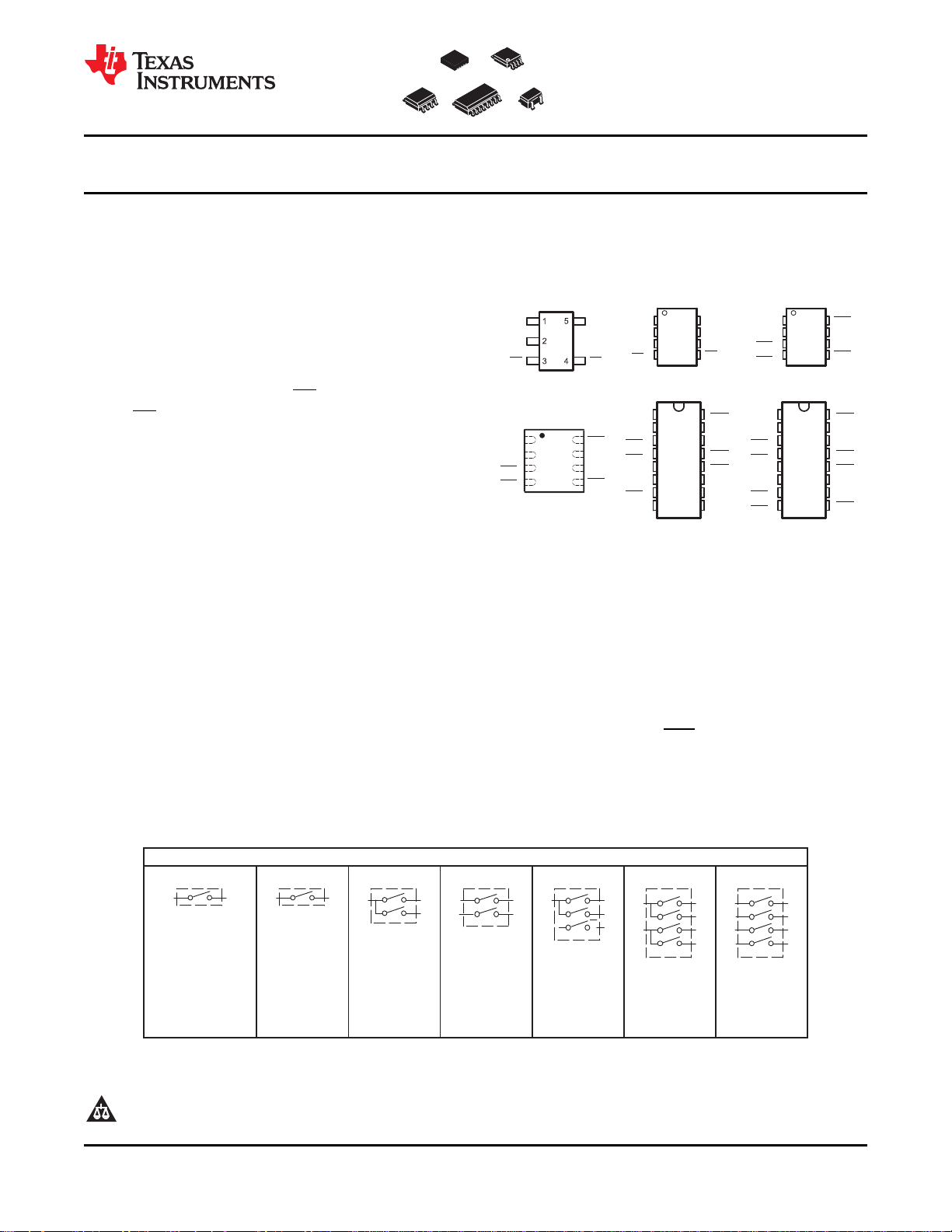
D−16
D−8
DBV−5
DRB−8
DGN−8
1
2
3
4
5
6
7
8
16
15
14
13
12
11
10
9
GND
IN2
EN3
†
NC
OC3
OUT3
NC
NC
1
2
3
4
8
7
6
5
GND
IN
IN
EN
†
OUT
OUT
OUT
OC
TPS2041B/TPS2051B
D ANDDGNPACKAGES
(TOP VIEW)
1
2
3
4
8
7
6
5
GND
GND
IN
IN
EN1
EN1
†
†
EN2
EN2
†
†
OC1
OC1
OUT1
OUT1
OUT2
OUT2
OC2
OC2
TPS2042B/TPS2052B
DRBPACKAGES
(TOP VIEW)
OC1
OUT1
OUT2
OC2
GND
IN1
EN1
†
EN2
†
1
2
3
4
5
6
7
8
16
15
14
13
12
11
10
9
GND
IN2
EN3
†
EN4
†
OC3
OUT3
OUT4
OC4
OC1
OUT1
OUT2
OC2
GND
IN1
EN1
†
EN2
†
− NoconnectNC
†
Allenableinputsareactivehighforthe TPS205xBseries.
TPS2044B/TPS2054B
D PACKAGE
(TOP VIEW)
TPS2043B/TPS2053B
DPACKAGE
(TOP VIEW)
GND
OUT
TPS2041B/TPS2051B
DBVPACKAGE
(TOP VIEW)
OC
IN
EN
†
4
3
2
1
5
6
7
8
TPS2042B/TPS2052B
D ANDDGNPACKAGES
(TOP VIEW)
TPS2014600mA
TPS20151 A
TPS2041B500mA
TPS2051B500mA
TPS2045A 250mA
TPS2049100mA
TPS2055A 250mA
TPS20611 A
TPS20651 A
TPS20681.5 A
TPS20691.5 A
TPS2042B500mA
TPS2052B500mA
TPS2046B250mA
TPS2056250mA
TPS20621 A
TPS20661 A
TPS20601.5 A
TPS20641.5 A
TPS2080500mA
TPS2081500mA
TPS2082500mA
TPS2090250mA
TPS2091250mA
TPS2092250mA
TPS2043B500mA
TPS2053B500mA
TPS2047B250mA
TPS2057A 250mA
TPS20631 A
TPS20671 A
TPS2044B500mA
TPS2054B500mA
TPS2048A 250mA
TPS2058250mA
TPS2085500mA
TPS2086500mA
TPS2087500mA
TPS2095250mA
TPS2096250mA
TPS2097250mA
TPS201xA 0.2 A to2A
TPS202x0.2 A to2A
TPS203x0.2 A to2A
GENERAL SWITCHCATALOG
33m ,SingleW 80m ,SingleW
80m ,DualW 80m ,DualW
80m , TripleW
80m ,QuadW 80m ,QuadW
TPS2043B, TPS2044B, TPS2051B
TPS2052B, TPS2053B, TPS2054B
www.ti.com
SLVS514L –JUNE 2010– REVISED JUNE 2011
CURRENT-LIMITED, POWER-DISTRIBUTION SWITCHES
Check for Samples: TPS2041B, TPS2042B, TPS2043B, TPS2044B, TPS2051B, TPS2052B, TPS2053B, TPS2054B
1
FEATURES
2
• 70-mΩ High-Side MOSFET
• 500-mA Continuous Current • Short-Circuit Protections
• Thermal and Short-Circuit Protection
• Accurate Current Limit
(0.75 A min, 1.25 A max)
• Operating Range: 2.7 V to 5.5 V
• 0.6-ms Typical Rise Time
• Undervoltage Lockout
• Deglitched Fault Report (OC)
• No OC Glitch During Power Up
• Maximum Standby Supply Current:
1-μA (Single, Dual) or 2-μA (Triple, Quad)
• Ambient Temperature Range: -40°C to 85°C
• UL Recognized, File Number E169910
• Additional UL Recognition for TPS2042B and
TPS2052B for Ganged Configuration
APPLICATIONS
• Heavy Capacitive Loads
TPS2041B, TPS2042B
DESCRIPTION
The TPS204xB/TPS205xB power-distribution switches are intended for applications where heavy capacitive
loads and short circuits are likely to be encountered. These devices incorporates 70-mΩ N-channel MOSFET
power switches for power-distribution systems that require multiple power switches in a single package. Each
switch is controlled by a logic enable input. Gate drive is provided by an internal charge pump designed to
control the power-switch rise times and fall times to minimize current surges during switching. The charge pump
requires no external components and allows operation from supplies as low as 2.7 V.
When the output load exceeds the current-limit threshold or a short is present, the device limits the output current
to a safe level by switching into a constant-current mode, pulling the overcurrent (OCx) logic output low. When
continuous heavy overloads and short-circuits increase the power dissipation in the switch, causing the junction
temperature to rise, a thermal protection circuit shuts off the switch to prevent damage. Recovery from a thermal
shutdown is automatic once the device has cooled sufficiently. Internal circuitry ensures that the switch remains
off until valid input voltage is present. This power-distribution switch is designed to set current limit at 1 A
typically.
1
2PowerPAD is a trademark of Texas Instruments.
UNLESS OTHERWISE NOTED this document contains
PRODUCTION DATA information current as of publication date.
Products conform to specifications per the terms of Texas
Instruments standard warranty. Production processing does not
necessarily include testing of all parameters.
See TI Switch Portfolio at http://www.ti.com/usbpower
Please be aware that an important notice concerning availability, standard warranty, and use in critical applications of Texas
Instruments semiconductor products and disclaimers thereto appears at the end of this data sheet.
Copyright © 2010–2011, Texas Instruments Incorporated
TPS2041B, TPS2042B
TPS2043B, TPS2044B, TPS2051B
TPS2052B, TPS2053B, TPS2054B
SLVS514L –JUNE 2010– REVISED JUNE 2011
These devices have limited built-in ESD protection. The leads should be shorted together or the device placed in conductive foam
during storage or handling to prevent electrostatic damage to the MOS gates.
www.ti.com
(1)
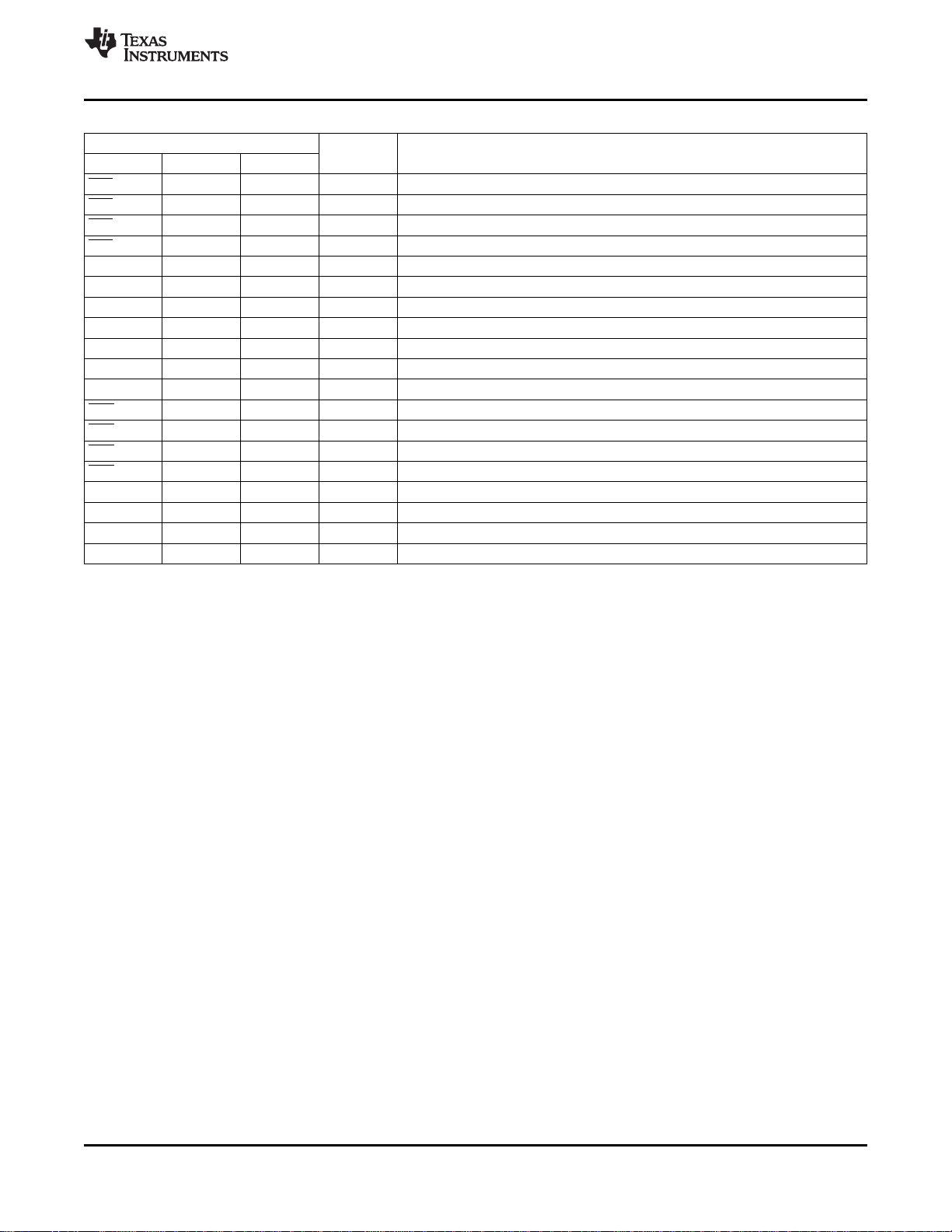
MSOP (DGN) SOIC (D) SOT-23 (DBV) SON (DRB)
T
A
-40°C to
85°C
DEVICE INFORMATION
RECOMMENDED SHORT-
ENABLE OF
Active low Single TPS2041BDGN TPS2041BD TPS2041BDBV
Active high Single TPS2051BDGN TPS2051BD TPS2051BDBV
Active low Dual TPS2042BDGN TPS2042BD TPS2042BDRB
Active high Dual TPS2052BDGN TPS2052BD TPS2052BDRB
Active low Triple -- TPS2043BD
Active high Triple -- TPS2053BD
Active low Quad -- TPS2044BD
Active high Quad -- TPS2054BD
MAXIMUM CIRCUIT
CONTINUOUS CURRENT
LOAD CURRENT LIMIT
0.5 A 1 A
TYPICAL PACKAGED DEVICES
NUMBER
SWITCHES
AT 25°C
(1) For the most current package and ordering information, see the Package Option Addendum at the end of this document, or see the TI
website at www.ti.com.
ABSOLUTE MAXIMUM RATINGS
over operating free-air temperature range unless otherwise noted
Input voltage range, V
Output voltage range, V
Input voltage range, V
Voltage range, V
I(/OC)
I(IN)
I(EN)
, V
O(OUT)
I(OCx)
Continuous output current, I
Continuous total power dissipation See Dissipation Rating Table
Operating virtual junction temperature range, T
Storage temperature range, T
Electrostatic discharge (ESD) protection
(1) Stresses beyond those listed under absolute maximum ratings may cause permanent damage to the device. These are stress ratings
only, and functional operation of the device at these or any other conditions beyond those indicated under recommended operating
conditions is not implied. Exposure to absolute-maximum-rated conditions for extended periods may affect device reliability.
(2) All voltages are with respect to GND.
, V
, V
I(INx)
, V
I(ENx)
O(OUT)
stg
(2)
O(OUTx)
, V
I(EN)
, I
O(OUTx)
(2)
, V
I(ENx)
J
Human body model (HBM) 2 kV
Charge device model (CDM) 500 V
(1)
UNIT
-0.3 V to 6 V
-0.3 V to 6 V
-0.3 V to 6 V
-0.3 V to 6 V
Internally limited
-40°C to 125°C
-65°C to 150°C
DISSIPATING RATING TABLE
PACKAGE
DGN-8 1712.3 mW 17.123 mW/°C 941.78 mW 684.93 mW
D-8 585.82 mW 5.8582 mW/°C 322.20 mW 234.32 mW
D-16 898.47 mW 8.9847 mW/°C 494.15 mW 359.38 mW
DBV-5 285 mW 2.85 mW/°C 155 mW 114 mW
DRB-8 (Low-K)
DRB-8 (High-K)
(1)
(2)
(1) Soldered PowerPAD on a standard 2-layer PCB without vias for thermal pad. See TI application note SLMA002 for further details.
(2) Soldered PowerPAD on a standard 4-layer PCB with vias for thermal pad. See TI application note SLMA002 for further details.
2 Copyright © 2010–2011, Texas Instruments Incorporated
THERMAL TA≤ 25°C DERATING FACTOR TA= 70°C TA= 85°C
RESISTANCE, θ
POWER RATING ABOVE TA= 25°C POWER RATING POWER RATING
JA
270 °CW 370 mW 3.71 mW/°C 203 mW 148 mW
60 °CW 1600 mW 16.67 mW/°C 916 mW 866 mW
TPS2041B, TPS2042B
TPS2043B, TPS2044B, TPS2051B
TPS2052B, TPS2053B, TPS2054B
www.ti.com
RECOMMENDED OPERATING CONDITIONS
Input voltage, V
Input voltage, V
Continuous output current, I
Operating virtual junction temperature, T
I(IN)
I(EN)
, V
, V
I(INx)
I(ENx)
, V
I(EN)
O(OUT)
, V
, I
O(OUTx)
I(ENx)
J
ELECTRICAL CHARACTERISTICS
over recommended operating junction temperature range, V
PARAMETER TEST CONDITIONS
POWER SWITCH
Static drain-source on-state D and DGN packages 70 135
resistance, 5-V operation mΩ
and 3.3-V operation
r
Static drain-source on-state V
DS(on)
resistance, 2.7-V operation -40°C ≤ TJ≤ 125°C
Static drain-source on-state V
resistance, 5-V operation connected, 0°C ≤ TJ≤ 70°C TPS2042B/52B
t
Rise time, output
r
t
Fall time, output
f
ENABLE INPUT EN AND ENx
V
High-level input voltage 2.7 V ≤ V
IH
V
Low-level input voltage 2.7 V ≤ V
IL
I
Input current V
I
t
Turnon time CL= 100 μF, RL= 10 Ω 3
on
t
Turnoff time CL= 100 μF, RL= 10 Ω 10
off
CURRENT LIMIT
I
Short-circuit output current A
OS
I
Overcurrent trip threshold VIN= 5 V, 100 A/s A
OC
SUPPLY CURRENT (TPS2041B, TPS2051B)
Supply current, low-level output μA
Supply current, high-level output μA
Leakage current -40°C ≤ TJ≤ 125°C 1 μA
Reverse leakage current V
(1) Pulse-testing techniques maintain junction temperature close to ambient temperature; thermal effects must be taken into account
separately.
V
= 5 V or 3.3 V, IO= 0.5 A,
I(IN)
-40°C ≤ TJ≤ 125°C
= 2.7 V, IO= 0.5 A,
I(IN)
= 5 V, IO= 1.0 A, OUT1 and OUT2 DGN package,
I(IN)
V
= 5.5 V 0.6 1.5
I(IN)
V
= 2.7 V 0.4 1
I(IN)
V
= 5.5 V 0.05 0.5
I(IN)
V
= 2.7 V 0.05 0.5
I(IN)
≤ 5.5 V 2
I(IN)
≤ 5.5 V 0.8
I(IN)
= 0 V or 5.5 V -0.5 0.5 μA
I(ENx)
V
= 5 V, OUT connected to GND,
I(IN)
device enabled into short-circuit
V
= 5 V, OUT1 and OUT2 connected to
I(IN)
GND, device enabled into short-circuit, 1.5
measure at IN
No load on OUT, V
or V
I(ENx)
= 0 V
No load on OUT, V
or V
I(ENx)
= 5.5 V
I(ENx)
I(ENx)
OUT connected to ground, V
or V
= 0 V
I(ENx)
= 5.5 V, IN = ground TJ= 25°C 0 μA
I(OUTx)
= 5.5 V, IO= 0.5 A, V
I(IN)
(1)
DBV package only 95 140
D and DGN packages 75 150 mΩ
CL= 1 μF,
RL= 10 Ω
TJ= 25°C ms
TJ= 25°C 0.75 1 1.25
-40°C ≤ TJ≤ 125°C 0.7 1 1.3
0°C ≤ TJ≤ 70°C
TPS2042B/52B
TPS2041B/51B I
TPS2042B/52B IOS1.55 2.0
= 5.5 V,
TJ= 25°C 0.5 1
-40°°C ≤ TJ≤ 125°C 0.5 5
= 0 V,
TJ= 25°C 43 60
-40°C ≤ TJ≤ 125°C 43 70
= 5.5 V,
I(ENx)
SLVS514L –JUNE 2010– REVISED JUNE 2011
MIN MAX UNIT
2.7 5.5 V
0 5.5 V
0 500 mA
-40 125 °C
= 0 V (unless otherwise noted)
I(/ENx)
MIN TYP MAX UNIT
49 mΩ
1.5 1.9
OS
V
ms
Copyright © 2010–2011, Texas Instruments Incorporated 3
TPS2041B, TPS2042B
TPS2043B, TPS2044B, TPS2051B
TPS2052B, TPS2053B, TPS2054B
SLVS514L –JUNE 2010– REVISED JUNE 2011
ELECTRICAL CHARACTERISTICS (continued)
over recommended operating junction temperature range, V
PARAMETER TEST CONDITIONS
SUPPLY CURRENT (TPS2042B, TPS2052B)
Supply current, low-level output No load on OUT, V
Supply current, high-level output No load on OUT, V
Leakage current OUT connected to ground, V
Reverse leakage current V
= 5.5 V, IN = ground TJ= 25°C 0.2 μA
I(OUTx)
SUPPLY CURRENT (TPS2043B, TPS2053B)
Supply current, low-level output No load on OUT, V
Supply current, high-level output No load on OUT, V
Leakage current OUT connected to ground, V
Reverse leakage current V
= 5.5 V, INx = ground TJ= 25°C 0.2 μA
I(OUTx)
SUPPLY CURRENT (TPS2044B, TPS2054B)
Supply current, low-level output μA
Supply current, high-level output μA
Leakage current -40°C≤ TJ≤ 125°C 1 μA
Reverse leakage current V
No load on OUT, V
or V
I(ENx)
= 0 V
No load on OUT, V
or V
I(ENx)
= 5.5 V
OUT connected to ground, V
or V
= 0 V
I(ENx)
= 5.5 V, INx = ground TJ= 25°C 0.2 μA
I(OUTx)
UNDERVOLTAGE LOCKOUT
Low-level input voltage, IN, INx 2 2.5 V
Hysteresis, IN, INx TJ= 25°C 75 mV
OVERCURRENT OC and OCx
Output low voltage, V
OL(/OCx)
Off-state current V
I
= 5 mA 0.4 V
O(OCx)
= 5 V or 3.3 V 1 μA
O(OCx)
OC deglitch OCx assertion or deassertion 4 8 15 ms
THERMAL SHUTDOWN
(2)
Thermal shutdown threshold 135 °C
Recovery from thermal shutdown 125 °C
Hysteresis 10 °C
(2) The thermal shutdown only reacts under overcurrent conditions.
I(ENx)
I(ENx)
I(ENx)
I(ENx)
I(ENx)
I(ENx)
= 5.5 V, IO= 0.5 A, V
I(IN)
= 5.5 V μA
= 0 V μA
= 5.5 V -40°C ≤ TJ≤ 125°C 1 μA
I(ENx)
= 0 V μA
= 5.5 V μA
= 0 V -40°C≤ TJ≤ 125°C 1 μA
I(ENx)
= 5.5 V,
(1)
TJ= 25°C 0.5 1
-40°C ≤ TJ≤ 125°C 0.5 5
TJ= 25°C 50 70
-40°C ≤ TJ≤ 125°C 50 90
TJ= 25°C 0.5 2
-40°C ≤ TJ≤ 125°C 0.5 10
TJ= 25°C 65 90
-40°C ≤ TJ≤ 125°C 65 110
TJ= 25°C 0.5 2
= 0 V (unless otherwise noted)
I(/ENx)
MIN TYP MAX UNIT
-40°C ≤ TJ≤ 125°C 0.5 10
= 0 V,
TJ= 25°C 75 110
-40°C ≤ TJ≤ 125°C 75 140
= 5.5 V,
I(ENx)
www.ti.com
4 Copyright © 2010–2011, Texas Instruments Incorporated
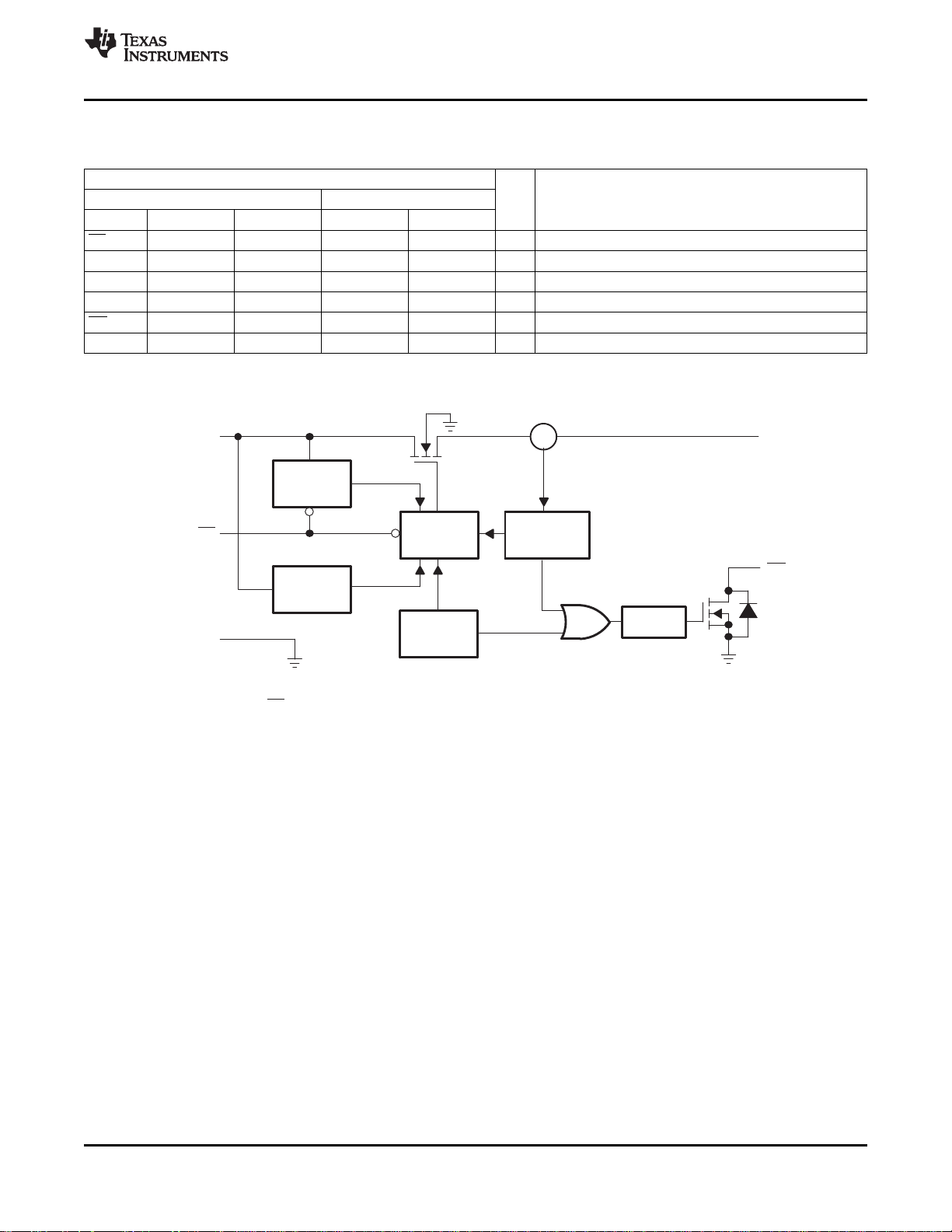
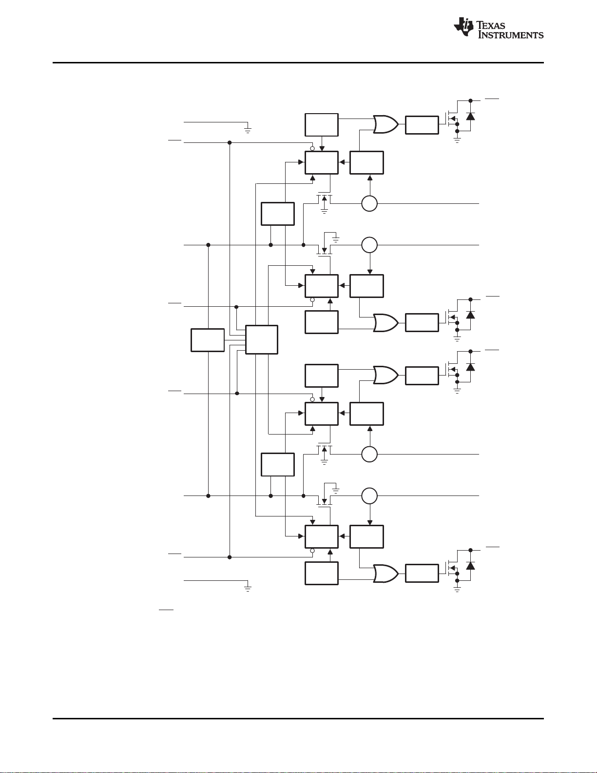
OUT
OC
IN
EN
GND
Current
Limit
Driver
UVLO
Charge
Pump
CS
Thermal
Sense
Deglitch
Note A: Current sense
Note B: Active low (EN
) for TPS2041B; Active high (EN) for TPS2051B
(See Note A)
(See Note B)
TPS2041B, TPS2042B
TPS2043B, TPS2044B, TPS2051B
TPS2052B, TPS2053B, TPS2054B
www.ti.com
DEVICE INFORMATION
Terminal Functions (TPS2041B and TPS2051B)
TERMINAL
D AND DGN PACKAGE DBV PACKAGE I/O DESCRIPTION
NAME TPS2041B TPS2051B TPS2041B TPS2051B
EN 4 – 4 – I Enable input, logic low turns on power switch
EN – 4 – 4 I Enable input, logic high turns on power switch
GND 1 1 2 2 Ground
IN 2, 3 2, 3 5 5 I Input voltage
OC 5 5 3 3 O Overcurrent open-drain output, active-low
OUT 6, 7, 8 6, 7, 8 1 1 O Power-switch output
Figure 1. Functional Block Diagram (TPS2041B and TPS2051B)
SLVS514L –JUNE 2010– REVISED JUNE 2011
Copyright © 2010–2011, Texas Instruments Incorporated 5
Thermal
Sense
Driver
Current
Limit
Charge
Pump
UVLO
CS
Driver
Current
Limit
CS
Thermal
Sense
Charge
Pump
GND
EN1
IN
EN2
OC1
OUT1
OUT2
OC2
Deglitch
Deglitch
(See Note A)
(See Note B)
Note A: Current sense
Note B: Active low (ENx
) for TPS2042B; Active high (ENx) for TPS2052B
(See Note B)
(See Note A)
TPS2041B, TPS2042B
TPS2043B, TPS2044B, TPS2051B
TPS2052B, TPS2053B, TPS2054B
SLVS514L –JUNE 2010– REVISED JUNE 2011
Terminal Functions (TPS2042B and TPS2052B)
TERMINAL
D, DGN, and DRB PACKAGES I/O DESCRIPTION
NAME TPS2042B TPS2052B
EN1 3 - I Enable input, logic low turns on power switch IN-OUT1
EN2 4 - I Enable input, logic low turns on power switch IN-OUT2
EN1 - 3 I Enable input, logic high turns on power switch IN-OUT1
EN2 - 4 I Enable input, logic high turns on power switch IN-OUT2
GND 1 1 Ground
IN 2 2 I Input voltage
OC1 8 8 O Overcurrent, open-drain output, active low, IN-OUT1
OC2 5 5 O Overcurrent, open-drain output, active low, IN-OUT2
OUT1 7 7 O Power-switch output, IN-OUT1
OUT2 6 6 O Power-switch output, IN-OUT2
PowerPAD™ - -
Functional Block Diagram (TPS2042B and TPS2052B)
Internally connected to GND; used to heat-sink the part to the circuit board
traces. Should be connected to GND pin.
www.ti.com
6 Copyright © 2010–2011, Texas Instruments Incorporated
TPS2043B, TPS2044B, TPS2051B
TPS2052B, TPS2053B, TPS2054B
www.ti.com
Terminal Functions (TPS2043B and TPS2053B)
TERMINAL
NAME TPS2043B TPS2053B
EN1 3 -- I Enable input, logic low turns on power switch IN1-OUT1
EN2 4 -- I Enable input, logic low turns on power switch IN1-OUT2
EN3 7 -- I Enable input, logic low turns on power switch IN2-OUT3
EN1 -- 3 I Enable input, logic high turns on power switch IN1-OUT1
EN2 -- 4 I Enable input, logic high turns on power switch IN1-OUT2
EN3 -- 7 I Enable input, logic high turns on power switch IN2-OUT3
GND 1, 5 1, 5 Ground
IN1 2 2 I Input voltage for OUT1 and OUT2
IN2 6 6 I Input voltage for OUT3
NC 8, 9, 10 8, 9, 10 No connection
OC1 16 16 O Overcurrent, open-drain output, active low, IN1-OUT1
OC2 13 13 O Overcurrent, open-drain output, active low, IN1-OUT2
OC3 12 12 O Overcurrent, open-drain output, active low, IN2-OUT3
OUT1 15 15 O Power-switch output, IN1-OUT1
OUT2 14 14 O Power-switch output, IN1-OUT2
OUT3 11 11 O Power-switch output, IN2-OUT3
I/O DESCRIPTION
SLVS514L –JUNE 2010– REVISED JUNE 2011
TPS2041B, TPS2042B
Copyright © 2010–2011, Texas Instruments Incorporated 7
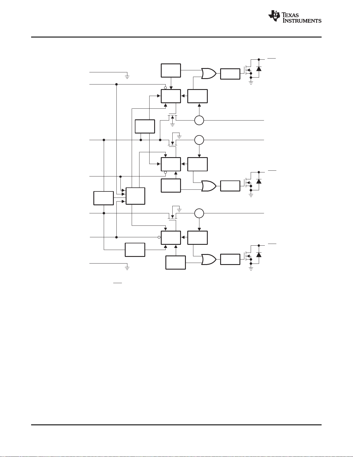
Thermal
Sense
Driver
Current
Limit
UVLO
CS
Driver
Current
Limit
CS
Thermal
Sense
GND
EN1
IN1
EN2
OC1
OUT1
OUT2
OC2
Deglitch
Deglitch
Driver
Current
Limit
CS
Thermal
Sense
Charge
Pump
GND
IN2
EN3
OUT3
OC3
Deglitch
VCC
Selector
UVLO
(See Note A)
Note A: Current sense
Note B: Active low (ENx
) for TPS2043B; Active high (ENx) for TPS2053B
(See Note A)
(See Note A)
(See Note B)
(See Note B)
(See Note B)
TPS2041B, TPS2042B
TPS2043B, TPS2044B, TPS2051B
TPS2052B, TPS2053B, TPS2054B
SLVS514L –JUNE 2010– REVISED JUNE 2011
Figure 2. Functional Block Diagram (TPS2043B and TPS2053B)
www.ti.com
8 Copyright © 2010–2011, Texas Instruments Incorporated
TPS2043B, TPS2044B, TPS2051B
TPS2052B, TPS2053B, TPS2054B
www.ti.com
Terminal Functions (TPS2044B and TPS2054B)
TERMINAL
NAME TPS2044B TPS2054B
EN1 3 - I Enable input, logic low turns on power switch IN1-OUT1
EN2 4 - I Enable input, logic low turns on power switch IN1-OUT2
EN3 7 - I Enable input, logic low turns on power switch IN2-OUT3
EN4 8 - I Enable input, logic low turns on power switch IN2-OUT4
EN1 - 3 I Enable input, logic high turns on power switch IN1-OUT1
EN2 - 4 I Enable input, logic high turns on power switch IN1-OUT2
EN3 - 7 I Enable input, logic high turns on power switch IN2-OUT3
EN4 - 8 I Enable input, logic high turns on power switch IN2-OUT4
GND 1, 5 1, 5 Ground
IN1 2 2 I Input voltage for OUT1 and OUT2
IN2 6 6 I Input voltage for OUT3 and OUT4
OC1 16 16 O Overcurrent, open-drain output, active low, IN1-OUT1
OC2 13 13 O Overcurrent, open-drain output, active low, IN1-OUT2
OC3 12 12 O Overcurrent, open-drain output, active low, IN2-OUT3
OC4 9 9 O Overcurrent, open-drain output, active low, IN2-OUT4
OUT1 15 15 O Power-switch output, IN1-OUT1
OUT2 14 14 O Power-switch output, IN1-OUT2
OUT3 11 11 O Power-switch output, IN2-OUT3
OUT4 10 10 O Power-switch output, IN2-OUT4
I/O DESCRIPTION
SLVS514L –JUNE 2010– REVISED JUNE 2011
TPS2041B, TPS2042B
Copyright © 2010–2011, Texas Instruments Incorporated 9
Thermal
Sense
Driver
Current
Limit
UVLO
CS
Driver
Current
Limit
CS
Thermal
Sense
Power Switch
GND
EN1
IN1
EN2
OC1
OUT1
OUT2
OC2
Deglitch
Deglitch
Thermal
Sense
Driver
Current
Limit
UVLO
CS
Driver
Current
Limit
CS
Thermal
Sense
Charge
Pump
Power Switch
GND
EN3
IN2
EN4
OC3
OUT3
OUT4
OC4
Deglitch
Deglitch
VCC
Selector
Note A: Current sense
Note B: Active low (ENx
) for TPS2044B; Active high (ENx) for TPS2054B
(See Note A)
(See Note A)
(See Note A)
(See Note A)
(See Note B)
(See Note B)
(See Note B)
(See Note B)
TPS2041B, TPS2042B
TPS2043B, TPS2044B, TPS2051B
TPS2052B, TPS2053B, TPS2054B
SLVS514L –JUNE 2010– REVISED JUNE 2011
Figure 3. Functional Block Diagram (TPS2044B and TPS2054B)
www.ti.com
10 Copyright © 2010–2011, Texas Instruments Incorporated
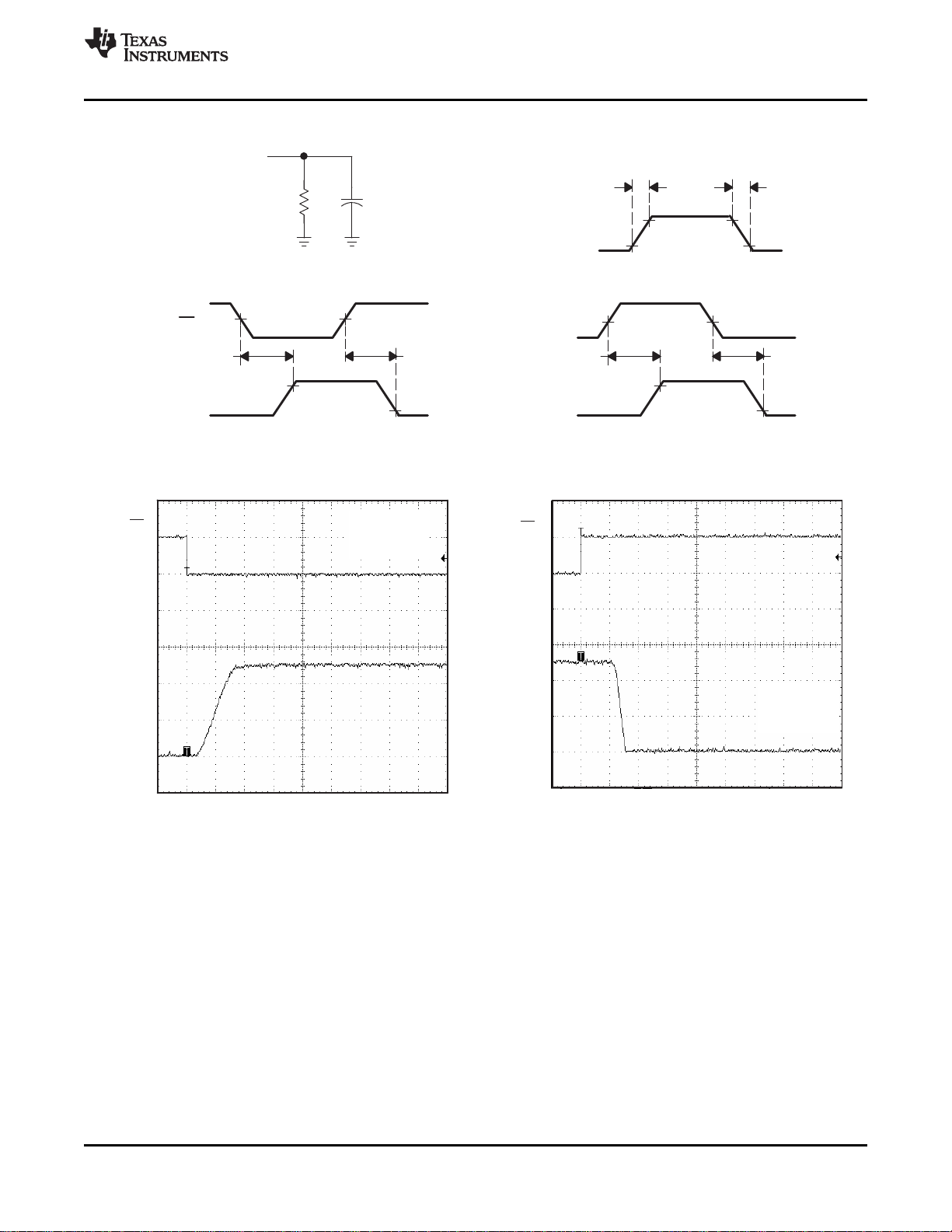
R
L
C
L
OUT
t
r
t
f
90%
90%
10%
10%
50%
50%
90%
10%
V
O(OUT)
V
I(EN)
V
O(OUT)
VOLTAGE WAVEFORMS
TEST CIRCUIT
t
on
t
off
50%
50%
90%
10%
V
I(EN)
V
O(OUT)
t
on
t
off
V
I(EN
)
V
I(EN)
5 V/div
V
O(OUT)
2 V/div
RL = 10 W,
CL = 1 mF
TA = 255C
t − Time − 500 ms/div
V
I(EN
)
V
I(EN)
5 V/div
V
O(OUT)
2 V/div
RL = 10 W,
CL = 1 mF
TA = 255C
t − Time − 500 ms/div
www.ti.com
TPS2041B, TPS2042B
TPS2043B, TPS2044B, TPS2051B
TPS2052B, TPS2053B, TPS2054B
SLVS514L –JUNE 2010– REVISED JUNE 2011
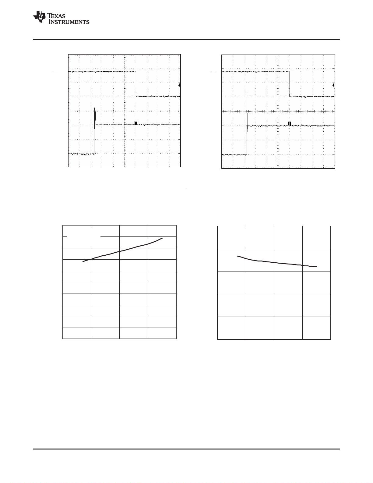
PARAMETER MEASUREMENT INFORMATION
Figure 4. Test Circuit and Voltage Waveforms
Figure 5. Turnon Delay and Rise Time With 1-μF Figure 6. Turnoff Delay and Fall Time With 1-μF
Load Load
Copyright © 2010–2011, Texas Instruments Incorporated 11
V
I(EN
)
V
I(EN)
5 V/div
V
O(OUT)
2 V/div
RL = 10 W,
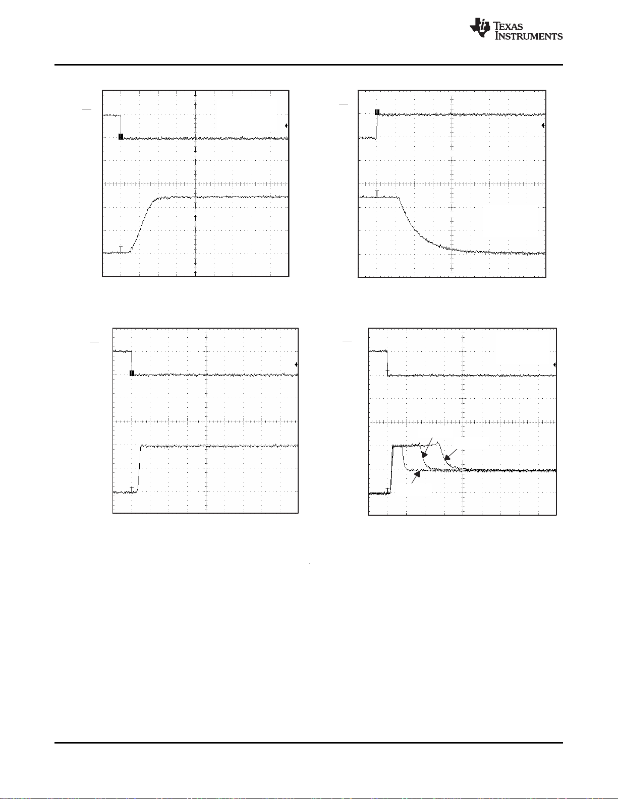
CL = 100 mF
TA = 255C
t − Time − 500 ms/div
V
O(OUT)
2 V/div
V
I(EN
)
V
I(EN)
5 V/div
RL = 10 W,
CL = 100 mF
TA = 255C
t − Time − 500 ms/div
220 mF
470 mF
100 mF
VI = 5 V ,
RL = 10 W,
TA = 255C
V
I(EN
)
V
I(EN)
5 V/div
I
O(OUT)
500 mA/div
t − Time − 500 ms/div
V
I(EN
)
V
I(EN)
5 V/div
I
O(OUT)
500 mA/div
t − Time − 500 ms/div
TPS2041B, TPS2042B
TPS2043B, TPS2044B, TPS2051B
TPS2052B, TPS2053B, TPS2054B
SLVS514L –JUNE 2010– REVISED JUNE 2011
PARAMETER MEASUREMENT INFORMATION (continued)
Figure 7. Turnon Delay and Rise Time With 100-μF Figure 8. Turnoff Delay and Fall Time With 100-μF
Load Load
www.ti.com
Figure 9. Short-Circuit Current, Figure 10. Inrush Current With Different
Device Enabled Into Short Load Capacitance
12 Copyright © 2010–2011, Texas Instruments Incorporated
V
O(OC
)
2 V/div
I
O(OUT)
500 mA/div
t − Time − 2 ms/div
V
O(OC
)
2 V/div
I
O(OUT)
500 mA/div
t − Time − 2 ms/div
0
0.1
0.2
0.3
0.4
0.5
0.6
0.7
0.8
0.9
1.0
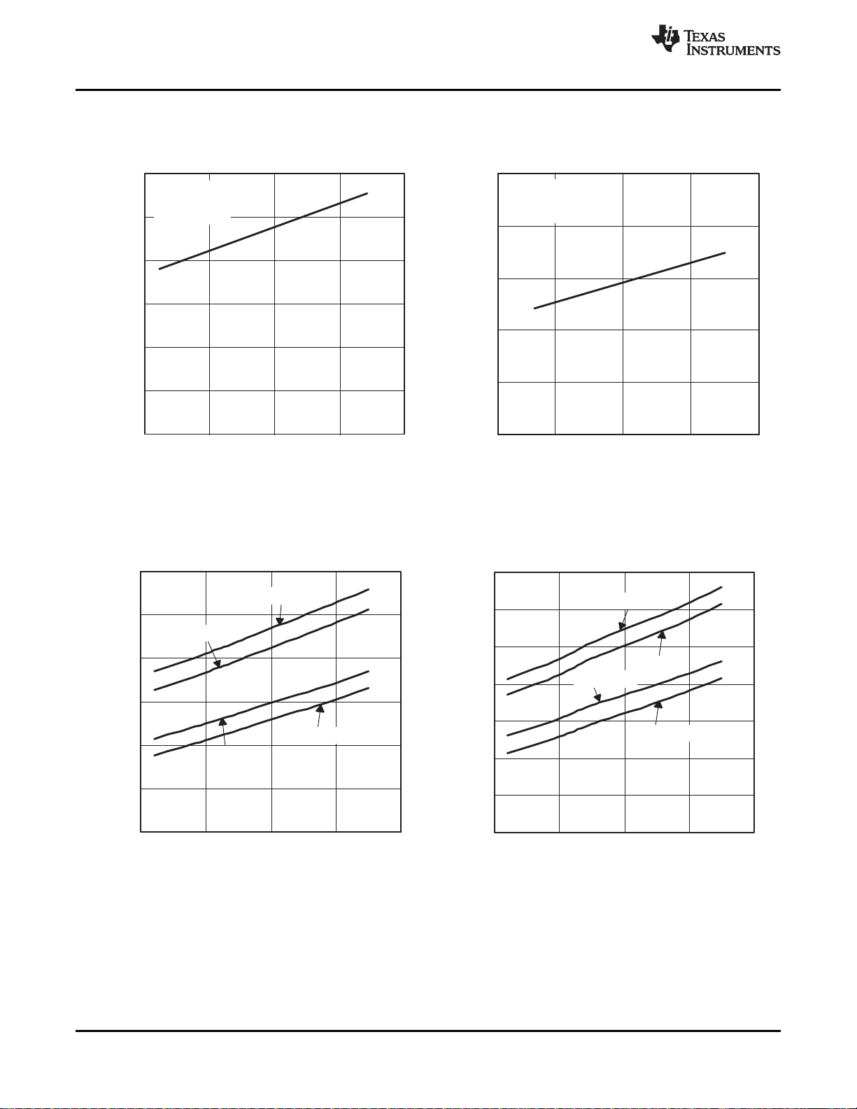
2 3 4 5 6
Turnon Time − ms
VI − Input Voltage − V
CL = 100 mF,
RL = 10 W,
TA = 255C
2.8
2.9
3
3.1
3.2
3.3
2 3 4 5 6
Turnoff Time − ms
VI − Input Voltage − V
CL = 100 mF,
RL = 10 W,
TA = 255C
TPS2041B, TPS2042B
TPS2043B, TPS2044B, TPS2051B
TPS2052B, TPS2053B, TPS2054B
www.ti.com
PARAMETER MEASUREMENT INFORMATION (continued)
Figure 11. 3-Ω Load Connected to Enabled Device Figure 12. 2-Ω Load Connected to Enabled Device
SLVS514L –JUNE 2010– REVISED JUNE 2011
TYPICAL CHARACTERISTICS
TURNON TIME TURNOFF TIME
vs vs
INPUT VOLTAGE INPUT VOLTAGE
Figure 13. Figure 14.
Copyright © 2010–2011, Texas Instruments Incorporated 13
0
0.1
0.2
0.3
0.4
0.5
0.6
2 3 4 5 6
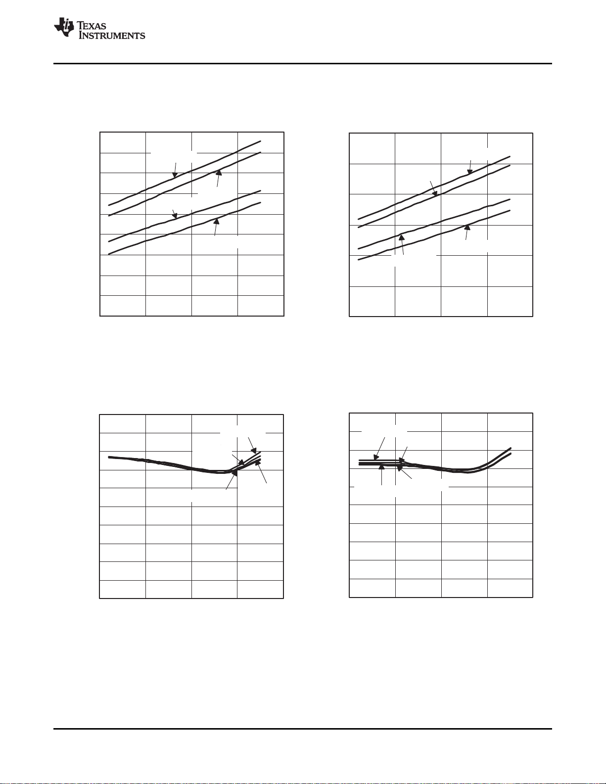
Rise Time − ms
VI − Input Voltage − V
CL = 1 mF,
RL = 10 W,
TA = 255C
0
0.05
0.1
0.15
0.2
0.25
2 3 4 5 6
CL = 1 mF,
RL = 10 W,
TA = 255C
Fall Time − ms
VI − Input Voltage − V
0
10
20
30
40
50
60
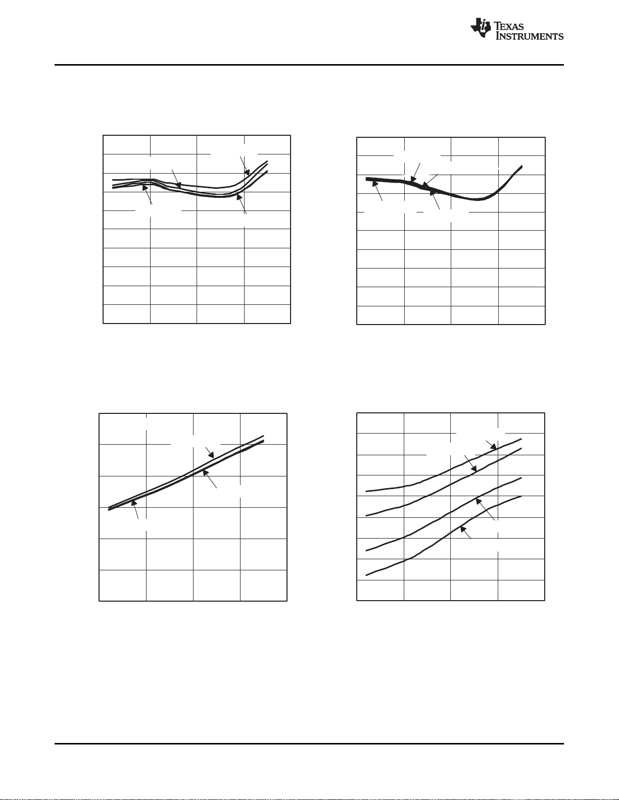
−50 0 50 100 150
VI = 5.5 V
VI = 3.3 V
VI = 2.7 V
TJ − Junction Temperature − 5C
− Supply Current, Output Enabled −
I
I (IN)
Aµ
VI = 5 V
0
10
20
30
40
50
60
70
−50 0 50 100 150
VI = 5.5 V
VI = 5 V
VI = 3.3 V
VI = 2.7 V
TJ − Junction Temperature − 5C
− Supply Current, Output Enabled −
I
I (IN)
Aµ
TPS2041B, TPS2042B
TPS2043B, TPS2044B, TPS2051B
TPS2052B, TPS2053B, TPS2054B
SLVS514L –JUNE 2010– REVISED JUNE 2011
TYPICAL CHARACTERISTICS (continued)
RISE TIME FALL TIME
vs vs
INPUT VOLTAGE INPUT VOLTAGE
www.ti.com
Figure 15. Figure 16.
TPS2041B/2051B TPS2042B/TPS2052B
SUPPLY CURRENT, OUTPUT ENABLED SUPPLY CURRENT, OUTPUT ENABLED
JUNCTION TEMPERATURE JUNCTION TEMPERATURE
14 Copyright © 2010–2011, Texas Instruments Incorporated
Figure 17. Figure 18.
vs vs
0
10
20
30
40
50
60
70
80
90
−50 0 50 100 150
VI = 5.5 V
VI = 5 V
VI = 3.3 V
VI = 2.7 V
TJ − Junction Temperature − 5C
− Supply Current, Output Enabled −
I
I (IN)
Aµ
0
20
40
60
80
100
120
−50 0 50 100 150
VI = 5.5 V
VI = 3.3 V
VI = 2.7 V
TJ − Junction Temperature − 5C
− Supply Current, Output Enabled −
I
I (IN)
Aµ
VI = 5 V
0
0.05
0.1
0.15
0.2
0.25
0.3
0.35
0.4
0.45
0.5
−50 0 50 100 150
VI = 5.5 V
VI = 5 V
VI = 3.3 V
VI = 2.7 V
TJ − Junction Temperature − 5C
− Supply Current, Output Disabled −
I
I (IN)
Aµ
TJ − Junction Temperature − 5C
− Supply Current, Output Disabled −I
I (IN)
Aµ
0
0.05
0.1
0.15
0.2
0.25
0.3
0.35
0.4
0.45
0.5
−50 0 50 100 150
VI = 2.7 V
VI = 3.3 V
VI = 5.5 V
VI = 5 V
www.ti.com
TPS2041B, TPS2042B
TPS2043B, TPS2044B, TPS2051B
TPS2052B, TPS2053B, TPS2054B
SLVS514L –JUNE 2010– REVISED JUNE 2011
TYPICAL CHARACTERISTICS (continued)
TPS2043B/TPS2053B TPS2044B/2054B
SUPPLY CURRENT, OUTPUT ENABLED SUPPLY CURRENT, OUTPUT ENABLED
vs vs
JUNCTION TEMPERATURE JUNCTION TEMPERATURE
Figure 19. Figure 20.
TPS2041B/2051B TPS2042B/TPS2052B
SUPPLY CURRENT, OUTPUT DISABLED SUPPLY CURRENT, OUTPUT DISABLED
JUNCTION TEMPERATURE JUNCTION TEMPERATURE
Copyright © 2010–2011, Texas Instruments Incorporated 15
Figure 21. Figure 22.
vs vs
0
0.05
0.1
0.15
0.2
0.25
0.3
0.35
0.4
0.45
0.5
−50 0 50 100 150
VI = 5.5 V
VI = 5 V
VI = 2.7 V
TJ − Junction Temperature − 5C
− Supply Current, Output Disabled −
I
I (IN)
Aµ
VI = 3.3 V
0
0.05
0.1
0.15
0.2
0.25
0.3
0.35
0.4
0.45
0.5
−50 0 50 100 150
VI = 5.5 V
VI = 5 V
VI = 2.7 V
TJ − Junction Temperature − 5C
− Supply Current, Output Disabled −I
I (IN)
Aµ
VI = 3.3 V
0.9
0.92
0.94
0.96
0.98
1.0
1.02
1.04
1.06
1.08
−50 0 50 100 150
VI = 5 V
VI = 3.3 V
VI = 5.5 V
TJ − Junction Temperature − 5C
VI = 2.7 V
− Short-Circuit Output Current − A
I
OS
0
20
40
60
80
100
120
−50 0 50 100 150
VI = 5 V
VI = 3.3 V
TJ − Junction Temperature − 5C
r
DS(on) − Static Drain-Source On-State Resistance − m
Ω
VI = 2.7 V
IO = 0.5 A
TPS2041B, TPS2042B
TPS2043B, TPS2044B, TPS2051B
TPS2052B, TPS2053B, TPS2054B
SLVS514L –JUNE 2010– REVISED JUNE 2011
TYPICAL CHARACTERISTICS (continued)
TPS2043B/TPS2053B TPS2044B/2054B
SUPPLY CURRENT, OUTPUT DISABLED SUPPLY CURRENT, OUTPUT DISABLED
vs vs
JUNCTION TEMPERATURE JUNCTION TEMPERATURE
www.ti.com
Figure 23. Figure 24.
STATIC DRAIN-SOURCE ON-STATE RESISTANCE SHORT-CIRCUIT OUTPUT CURRENT
JUNCTION TEMPERATURE JUNCTION TEMPERATURE
16 Copyright © 2010–2011, Texas Instruments Incorporated
Figure 25. Figure 26.
vs vs

1
1.2
1.4
1.6
1.8
2
2.5 3 3.5 4 4.5 5 5.5 6
TA = 255C
Load Ramp = 1A/10 ms
Threshold Trip Current − A
VI − Input Voltage − V
TPS2043B,
TPS2044B,
TPS2053B,
TPS2054B
Threshold Trip Current − A
VI − Input Voltage − V
1
1.2
1.4
1.6
1.8
2
2.5 3 3.5 4 4.5 5 5.5 6
TA = 255C
Load Ramp = 1A/10 ms
TPS2041B,
TPS2042B,
TPS2051B,
TPS2052B
0
20
40
60
80
100
0 2.5 5 7.5 10 12.5
Peak Current − A
VI = 5 V ,
TA = 255C
Current-Limit Response − sµ
2.1
2.14
2.18
2.22
2.26
2.3
−50 0 50 100 150
UVLO Rising
UVLO Falling
UVLO − Undervoltage Lockout − V
TJ − Junction Temperature − 5C
www.ti.com
TPS2041B, TPS2042B
TPS2043B, TPS2044B, TPS2051B
TPS2052B, TPS2053B, TPS2054B
SLVS514L –JUNE 2010– REVISED JUNE 2011
TYPICAL CHARACTERISTICS (continued)
THRESHOLD TRIP CURRENT THRESHOLD TRIP CURRENT
vs vs
INPUT VOLTAGE INPUT VOLTAGE
UNDERVOLTAGE LOCKOUT CURRENT-LIMIT RESPONSE
JUNCTION TEMPERATURE PEAK CURRENT
Figure 27. Figure 28.
vs vs
Figure 29. Figure 30.
Copyright © 2010–2011, Texas Instruments Incorporated 17

IN
OC1
EN1
OC2
2
8
5
7
0.1 µF 22 µF
0.1 µF 22 µF
Load
Load
OUT1
OUT2
Power Supply
2.7 V to 5.5 V
6
EN2
3
4
GND
0.1 µF
TPS2042B
1
TPS2041B, TPS2042B
TPS2043B, TPS2044B, TPS2051B
TPS2052B, TPS2053B, TPS2054B
SLVS514L –JUNE 2010– REVISED JUNE 2011
APPLICATION INFORMATION
POWER-SUPPLY CONSIDERATIONS
Figure 31. Typical Application (Example, TPS2042B)
www.ti.com
A 0.01-μF to 0.1-μF ceramic bypass capacitor between IN and GND, close to the device, is recommended.
Placing a high-value electrolytic capacitor on the output pin(s) is recommended when the output load is heavy.
This precaution reduces power-supply transients that may cause ringing on the input. Additionally, bypassing the
output with a 0.01-μF to 0.1-μF ceramic capacitor improves the immunity of the device to short-circuit transients.
OVERCURRENT
A sense FET is employed to check for overcurrent conditions. Unlike current-sense resistors, sense FETs do not
increase the series resistance of the current path. When an overcurrent condition is detected, the device
maintains a constant output current and reduces the output voltage accordingly. Complete shutdown occurs only
if the fault is present long enough to activate thermal limiting.
Three possible overload conditions can occur. In the first condition, the output has been shorted before the
device is enabled or before V
has been applied (see Figure 17 through Figure 20). The TPS204xB/TPS205xB
I(IN)
senses the short and immediately switches into a constant-current output.
In the second condition, a short or an overload occurs while the device is enabled. At the instant the overload
occurs, high currents may flow for a short period of time before the current-limit circuit can react. After the
current-limit circuit has tripped (reached the overcurrent trip threshold), the device switches into constant-current
mode.
In the third condition, the load has been gradually increased beyond the recommended operating current. The
current is permitted to rise until the current-limit threshold is reached or until the thermal limit of the device is
exceeded (see Figure 21 through Figure 24). The TPS204xB/TPS205xB is capable of delivering current up to the
current-limit threshold without damaging the device. Once the threshold has been reached, the device switches
into its constant-current mode.
OC RESPONSE
The OCx open-drain output is asserted (active low) when an overcurrent or overtemperature shutdown condition
is encountered after a 10-ms deglitch timeout. The output remains asserted until the overcurrent or
overtemperature condition is removed. Connecting a heavy capacitive load to an enabled device can cause a
momentary overcurrent condition; however, no false reporting on OCx occurs due to the 10-ms deglitch circuit.
The TPS204xB/TPS205xB is designed to eliminate false overcurrent reporting. The internal overcurrent deglitch
eliminates the need for external components to remove unwanted pulses. OCx is not deglitched when the switch
is turned off due to an overtemperature shutdown.
18 Copyright © 2010–2011, Texas Instruments Incorporated

GND
IN
EN1
EN2
OC1
OC2
OUT1
OUT2
TPS2042B
R
pullup
V+
TPS2041B, TPS2042B
TPS2043B, TPS2044B, TPS2051B
TPS2052B, TPS2053B, TPS2054B
www.ti.com
Figure 32. Typical Circuit for the OC Pin (Example, TPS2042B)
POWER DISSIPATION AND JUNCTION TEMPERATURE
The low on-resistance on the N-channel MOSFET allows the small surface-mount packages to pass large
currents. The thermal resistances of these packages are high compared to those of power packages; it is good
design practice to check power dissipation and junction temperature. Begin by determining the r
N-channel MOSFET relative to the input voltage and operating temperature. As an initial estimate, use the
highest operating ambient temperature of interest and read r
dissipation per switch can be calculated by:
PD= r
DS(on)
× I
2
Multiply this number by the number of switches being used. This step renders the total power dissipation from
the N-channel MOSFETs.
Finally, calculate the junction temperature:
TJ= PD× R
θJA
+ T
A
Where:
TA= Ambient temperature °C
R
= Thermal resistance
θJA
PD= Total power dissipation based on number of switches being used.
from Figure 25. Using this value, the power
DS(on)
SLVS514L –JUNE 2010– REVISED JUNE 2011
of the
DS(on)
Compare the calculated junction temperature with the initial estimate. If they do not agree within a few degrees,
repeat the calculation, using the calculated value as the new estimate. Two or three iterations are generally
sufficient to get a reasonable answer.
THERMAL PROTECTION
Thermal protection prevents damage to the IC when heavy-overload or short-circuit faults are present for
extended periods of time. The TPS204xB/TPS205xB implements a thermal sensing to monitor the operating
junction temperature of the power distribution switch. In an overcurrent or short-circuit condition, the junction
temperature rises due to excessive power dissipation. Once the die temperature rises to approximately 140°C
due to overcurrent conditions, the internal thermal sense circuitry turns the power switch off, thus preventing the
power switch from damage. Hysteresis is built into the thermal sense circuit, and after the device has cooled
approximately 10°C, the switch turns back on. The switch continues to cycle in this manner until the load fault or
input power is removed. The OCx open-drain output is asserted (active low) when an overtemperature shutdown
or overcurrent occurs.
UNDERVOLTAGE LOCKOUT (UVLO)
An undervoltage lockout ensures that the power switch is in the off state at power up. Whenever the input
voltage falls below approximately 2 V, the power switch is quickly turned off. This facilitates the design of
hot-insertion systems where it is not possible to turn off the power switch before input power is removed. The
UVLO also keeps the switch from being turned on until the power supply has reached at least 2 V, even if the
switch is enabled. On reinsertion, the power switch is turned on, with a controlled rise time to reduce EMI and
voltage overshoots.
Copyright © 2010–2011, Texas Instruments Incorporated 19

IN
OC
EN
GND
0.1 µF
2, 3
5
4
6, 7, 8
0.1 µF 120 µF
GND
OUT
TPS2041B
Power Supply
D+
D−
V
BUS
Downstream
USB Ports
USB
Control
3.3 V 5 V
1
TPS2041B, TPS2042B
TPS2043B, TPS2044B, TPS2051B
TPS2052B, TPS2053B, TPS2054B
SLVS514L –JUNE 2010– REVISED JUNE 2011
UNIVERSAL SERIAL BUS (USB) APPLICATIONS
The universal serial bus (USB) interface is a 12-Mb/s, or 1.5-Mb/s, multiplexed serial bus designed for
low-to-medium bandwidth PC peripherals (e.g., keyboards, printers, scanners, and mice). The four-wire USB
interface is conceived for dynamic attach-detach (hot plug-unplug) of peripherals. Two lines are provided for
differential data, and two lines are provided for 5-V power distribution.
USB data is a 3.3-V level signal, but power is distributed at 5 V to allow for voltage drops in cases where power
is distributed through more than one hub across long cables. Each function must provide its own regulated 3.3 V
from the 5-V input or its own internal power supply.
The USB specification defines the following five classes of devices, each differentiated by power-consumption
requirements:
• Hosts/self-powered hubs (SPH)
• Bus-powered hubs (BPH)
• Low-power, bus-powered functions
• High-power, bus-powered functions
• Self-powered functions
Self-powered and bus-powered hubs distribute data and power to downstream functions. The
TPS204xB/TPS205xB can provide-power distribution solutions to many of these classes of devices.
www.ti.com
HOST/SELF-POWERED AND BUS-POWERED HUBS
Hosts and self-powered hubs have a local power supply that powers the embedded functions and the
downstream ports (see Figure 33 and Figure 34). This power supply must provide from 5.25 V to 4.75 V to the
board side of the downstream connection under full-load and no-load conditions. Hosts and SPHs are required to
have current-limit protection and must report overcurrent conditions to the USB controller. Typical SPHs are
desktop PCs, monitors, printers, and stand-alone hubs.
Figure 33. Typical One-Port USB Host / Self-Powered Hub
20 Copyright © 2010–2011, Texas Instruments Incorporated

IN1
OC1
EN1
OC2
EN2
GND
0.1 µF
2
16
3
13
4
15
14
33 µF
33 µF
GND
1
OUT1
OUT2
TPS2044B
Power Supply
D+
D−
V
BUS
GND
D+
D−
V
BUS
Downstream
USB Ports
USB
Controller
3.3 V 5 V
OC3
EN3
OC4
EN4
12
7
9
8
6
IN2
+
+
5
GND
11
10
33 µF
33 µF
GND
OUT3
OUT4
D+
D−
V
BUS
GND
D+
D−
V
BUS
+
+
www.ti.com
TPS2041B, TPS2042B
TPS2043B, TPS2044B, TPS2051B
TPS2052B, TPS2053B, TPS2054B
SLVS514L –JUNE 2010– REVISED JUNE 2011
Figure 34. Typical Four-Port USB Host / Self-Powered Hub
Bus-powered hubs obtain all power from upstream ports and often contain an embedded function. The hubs are
required to power up with less than one unit load. The BPH usually has one embedded function, and power is
always available to the controller of the hub. If the embedded function and hub require more than 100 mA on
power up, the power to the embedded function may need to be kept off until enumeration is completed. This can
be accomplished by removing power or by shutting off the clock to the embedded function. Power switching the
embedded function is not necessary if the aggregate power draw for the function and controller is less than one
unit load. The total current drawn by the bus-powered device is the sum of the current to the controller, the
embedded function, and the downstream ports, and it is limited to 500 mA from an upstream port.
LOW-POWER BUS-POWERED AND HIGH-POWER BUS-POWERED FUNCTIONS
Both low-power and high-power bus-powered functions obtain all power from upstream ports; low-power
functions always draw less than 100 mA; high-power functions must draw less than 100 mA at power up and can
draw up to 500 mA after enumeration. If the load of the function is more than the parallel combination of 44 Ω
and 10 μF at power up, the device must implement inrush current limiting (see Figure 35).
Copyright © 2010–2011, Texas Instruments Incorporated 21

IN
OC1
OC2
2
8
3
5
4
7
0.1 µF 10 µF
Internal
Function
OUT1
Power Supply
3.3 V
EN1
6
0.1 µF 10 µF
OUT2
Internal
Function
0.1 µF
10 µF
USB
Control
GND
V
BUS
D−
D+
EN2
GND
1
TPS2042B
TPS2041B, TPS2042B
TPS2043B, TPS2044B, TPS2051B
TPS2052B, TPS2053B, TPS2054B
SLVS514L –JUNE 2010– REVISED JUNE 2011
Figure 35. High-Power Bus-Powered Function (Example, TPS2042B)
USB POWER-DISTRIBUTION REQUIREMENTS
USB can be implemented in several ways, and, regardless of the type of USB device being developed, several
power-distribution features must be implemented.
• Hosts/self-powered hubs must:
– Current-limit downstream ports
– Report overcurrent conditions on USB V
• Bus-powered hubs must:
– Enable/disable power to downstream ports
– Power up at <100 mA
– Limit inrush current (<44 Ω and 10 μF)
• Functions must:
– Limit inrush currents
– Power up at <100 mA
The feature set of the TPS204xB/TPS205xB allows them to meet each of these requirements. The integrated
current-limiting and overcurrent reporting is required by hosts and self-powered hubs. The logic-level enable and
controlled rise times meet the need of both input and output ports on bus-powered hubs, as well as the input
ports for bus-powered functions (see Figure 36 through Figure 39).
BUS
www.ti.com
22 Copyright © 2010–2011, Texas Instruments Incorporated

†
USB rev 1.1 requires 120 µF per hub.
DP1
DM1
DP2
DM2
DP3
DM3
DP4
PWRON1
OVRCUR1
PWRON2
OVRCUR2
PWRON3
OVRCUR3
PWRON4
OVRCUR4
DM4
DP0
DM0
V
CC
XTAL1
XTAL2
OCSOFF
SN75240
D +
D −
5 V
GND
D +
D −
5 V
D +
D −
5 V
D +
D −
5 V
48-MHz
Crystal
Downstream
Ports
TUSB2041B
Hub Controller
Tuning
Circuit
ABC
D
33 µF
†
SN75240
ABC
D
GND
GND
GND
33 µF
†
33 µF
†
33 µF
†
D +
D −
Upstream
Port
TPS2041B
SN75240
A
B
5 V
GND
C
D
1 µF
IN
GND
Ferrite Beads
Ferrite Beads
Ferrite Beads
Ferrite Beads
BUSPWR
GANGED
Tie to TPS2041B EN
Input
OC EN
OUT
5-V Power
Supply
IN
GND
3.3 V
4.7 µF
0.1 µF
4.7 µF
GND
EN
OC
IN
TPS2041B
OUT
EN
OC
IN
TPS2041B
OUT
EN
OC
IN
TPS2041B
OUT
EN
OC
IN
TPS2041B
OUT
TPS76333
0.1 µF
0.1 µF
0.1 µF
0.1 µF
www.ti.com
TPS2041B, TPS2042B
TPS2043B, TPS2044B, TPS2051B
TPS2052B, TPS2053B, TPS2054B
SLVS514L –JUNE 2010– REVISED JUNE 2011
Copyright © 2010–2011, Texas Instruments Incorporated 23
Figure 36. Hybrid Self / Bus-Powered Hub Implementation, TPS2041B/TPS2051B

DP1
DM1
DP2
DM2
DP3
DM3
DP4
PWRON1
OVRCUR1
PWRON2
OVRCUR2
DM4
DP0
DM0
V
CC
XTAL1
XTAL2
OCSOFF
SN75240
D +
D −
5 V
GND
D +
D −
5 V
D +
D −
5 V
D +
D −
5 V
48-MHz
Crystal
Downstream
Ports
TUSB2040
Hub Controller
Tuning
Circuit
ABC
D
33 µF
†
SN75240
ABC
D
GND
GND
GND
33 µF
†
33 µF
†
33 µF
†
D +
D −
Upstream
Port
TPS2041B
SN75240
A
B
5 V
GND
C
D
1 µF
IN
GND
Ferrite Beads
Ferrite Beads
Ferrite Beads
Ferrite Beads
BUSPWR
GANGED
Tie to TPS2041B EN
Input
OC EN
OUT
5-V Power
Supply
IN
GND
3.3 V
4.7 µF
0.1 µF
4.7 µF
EN1
IN
OC1
OUT1
TPS2042B
EN2
OC2
OUT2
0.1 µF
GND
†
USB rev 1.1 requires 120 µF per hub.
TPS76333
PWRON3
PWRON4
OVRCUR3
OVRCUR4
EN1
IN
OC1
OUT1
TPS2042B
EN2
OC2
OUT2
0.1 µF
TPS2041B, TPS2042B
TPS2043B, TPS2044B, TPS2051B
TPS2052B, TPS2053B, TPS2054B
SLVS514L –JUNE 2010– REVISED JUNE 2011
www.ti.com
Figure 37. Hybrid Self / Bus-Powered Hub Implementation, TPS2042B/TPS2052B
24 Copyright © 2010–2011, Texas Instruments Incorporated

DP1
DM1
DP2
DM2
DP3
DM3
PWRON1
OVRCUR1
PWRON2
OVRCUR2
PWRON3
OVRCUR3
DP0
DM0
V
CC
XTAL1
XTAL2
OCSOFF
SN75240
D +
D −
5 V
GND
D +
D −
5 V
D +
D −
5 V
48-MHz
Crystal
Downstream
Ports
TUSB2040
Hub Controller
Tuning
Circuit
ABC
D
47 µF
†
1/2 SN75240
ABC
D
GND
GND
47 µF
†
47 µF
†
D +
D −
Upstream
Port
TPS2041B
1/2 SN75240
A
B
5 V
GND
C
D
1 µF
IN
GND
Ferrite Beads
Ferrite Beads
Ferrite Beads
BUSPWR
GANGED
Tie to TPS2041B EN
Input
OC EN
OUT
5-V Power
Supply
IN
GND
3.3 V
4.7 µF
0.1 µF
4.7 µF
EN1
IN1
OC1
OUT1
TPS2053B
EN2
OC2
OUT2
0.1 µF
0.1 µF
GND
†
USB rev 1.1 requires 120 µF per hub.
OUT3
EN3
OC3
IN2
GND
GND
TPS76333
www.ti.com
TPS2041B, TPS2042B
TPS2043B, TPS2044B, TPS2051B
TPS2052B, TPS2053B, TPS2054B
SLVS514L –JUNE 2010– REVISED JUNE 2011
Figure 38. Hybrid Self / Bus-Powered Hub Implementation, TPS2043B/TPS2053B
Copyright © 2010–2011, Texas Instruments Incorporated 25

DP1
DM1
DP2
DM2
DP3
DM3
DP4
PWRON1
OVRCUR1
PWRON2
OVRCUR2
PWRON3
OVRCUR3
PWRON4
OVRCUR4
DM4
DP0
DM0
V
CC
XTAL1
XTAL2
OCSOFF
SN75240
D +
D −
5 V
GND
D +
D −
5 V
D +
D −
5 V
D +
D −
5 V
48-MHz
Crystal
Downstream
Ports
TUSB2040
Hub Controller
Tuning
Circuit
ABC
D
33 µF
†
SN75240
ABC
D
GND
GND
GND
33 µF
†
33 µF
†
33 µF
†
D +
D −
Upstream
Port
TPS2041B
SN75240
A
B
5 V
GND
C
D
1 µF
IN
GND
Ferrite Beads
Ferrite Beads
Ferrite Beads
Ferrite Beads
BUSPWR
GANGED
Tie to TPS2041B EN
Input
OC EN
OUT
5-V Power
Supply
IN
GND
3.3 V
4.7 µF
0.1 µF
4.7 µF
EN1
IN1
OC1
OUT1
TPS2044B
EN2
OC2
OUT2
0.1 µF
0.1 µF
GND
†
USB rev 1.1 requires 120 µF per hub.
EN3
OC3
OUT3
EN4
OC4
OUT4
IN2
GND1
GND2
TPS76333
TPS2041B, TPS2042B
TPS2043B, TPS2044B, TPS2051B
TPS2052B, TPS2053B, TPS2054B
SLVS514L –JUNE 2010– REVISED JUNE 2011
www.ti.com
Figure 39. Hybrid Self / Bus-Powered Hub Implementation, TPS2044B/TPS2054B
26 Copyright © 2010–2011, Texas Instruments Incorporated

Power
Supply
0.1 µF
1000 µF
Optimum
2.7 V to 5.5 V
PC Board
Overcurrent Response
TPS2042B
OC1
GND
EN1
IN
EN2
OUT1
OUT2
OC2
Block of
Circuitry
Block of
Circuitry
TPS2041B, TPS2042B
TPS2043B, TPS2044B, TPS2051B
TPS2052B, TPS2053B, TPS2054B
www.ti.com
GENERIC HOT-PLUG APPLICATIONS
In many applications it may be necessary to remove modules or pc boards while the main unit is still operating.
These are considered hot-plug applications. Such implementations require the control of current surges seen by
the main power supply and the card being inserted. The most effective way to control these surges is to limit and
slowly ramp the current and voltage being applied to the card, similar to the way in which a power supply
normally turns on. Due to the controlled rise times and fall times of the TPS204xB/TPS205xB, these devices can
be used to provide a softer start-up to devices being hot-plugged into a powered system. The UVLO feature of
the TPS204xB/TPS205xB also ensures that the switch is off after the card has been removed, and that the
switch is off during the next insertion. The UVLO feature insures a soft start with a controlled rise time for every
insertion of the card or module.
SLVS514L –JUNE 2010– REVISED JUNE 2011
Figure 40. Typical Hot-Plug Implementation (Example, TPS2042B)
By placing the TPS204xB/TPS205xB between the VCCinput and the rest of the circuitry, the input power reaches
these devices first after insertion. The typical rise time of the switch is approximately 1 ms, providing a slow
voltage ramp at the output of the device. This implementation controls system surge currents and provides a
hot-plugging mechanism for any device.
DETAILED DESCRIPTION
Power Switch
The power switch is an N-channel MOSFET with a low on-state resistance. Configured as a high-side switch, the
power switch prevents current flow from OUT to IN and IN to OUT when disabled. The power switch supplies a
minimum current of 500 mA.
Charge Pump
An internal charge pump supplies power to the driver circuit and provides the necessary voltage to pull the gate
of the MOSFET above the source. The charge pump operates from input voltages as low as 2.7 V and requires
little supply current.
Driver
The driver controls the gate voltage of the power switch. To limit large current surges and reduce the associated
electromagnetic interference (EMI) produced, the driver incorporates circuitry that controls the rise times and fall
times of the output voltage.
Enable (ENx)
The logic enable pin disables the power switch and the bias for the charge pump, driver, and other circuitry to
reduce the supply current. The supply current is reduced to less than 1 μA or 2 μA when a logic high is present
on EN. A logic zero input on EN restores bias to the drive and control circuits and turns the switch on. The
enable input is compatible with both TTL and CMOS logic levels.
Copyright © 2010–2011, Texas Instruments Incorporated 27

TPS2041B, TPS2042B
TPS2043B, TPS2044B, TPS2051B
TPS2052B, TPS2053B, TPS2054B
SLVS514L –JUNE 2010– REVISED JUNE 2011
Enable (ENx)
The logic enable disables the power switch and the bias for the charge pump, driver, and other circuitry to reduce
the supply current. The supply current is reduced to less than 1 μA or 2 μA when a logic low is present on ENx.
A logic high input on ENx restores bias to the drive and control circuits and turns the switch on. The enable input
is compatible with both TTL and CMOS logic levels.
Overcurrent (OCx)
The OCx open-drain output is asserted (active low) when an overcurrent or overtemperature condition is
encountered. The output remains asserted until the overcurrent or overtemperature condition is removed. A
10-ms deglitch circuit prevents the OCx signal from oscillation or false triggering. If an overtemperature shutdown
occurs, the OCx is asserted instantaneously.
Current Sense
A sense FET monitors the current supplied to the load. The sense FET measures current more efficiently than
conventional resistance methods. When an overload or short circuit is encountered, the current-sense circuitry
sends a control signal to the driver. The driver in turn reduces the gate voltage and drives the power FET into its
saturation region, which switches the output into a constant-current mode and holds the current constant while
varying the voltage on the load.
www.ti.com
Thermal Sense
The TPS204xB/TPS205xB implements a thermal sensing to monitor the operating temperature of the power
distribution switch. In an overcurrent or short-circuit condition, the junction temperature rises. When the die
temperature rises to approximately 140°C due to overcurrent conditions, the internal thermal sense circuitry turns
off the switch, thus preventing the device from damage. Hysteresis is built into the thermal sense, and after the
device has cooled approximately 10 degrees, the switch turns back on. The switch continues to cycle off and on
until the fault is removed. The open-drain false reporting output (OCx) is asserted (active low) when an
overtemperature shutdown or overcurrent occurs.
Undervoltage Lockout
A voltage sense circuit monitors the input voltage. When the input voltage is below approximately 2 V, a control
signal turns off the power switch.
28 Copyright © 2010–2011, Texas Instruments Incorporated

TPS2041B, TPS2042B
TPS2043B, TPS2044B, TPS2051B
TPS2052B, TPS2053B, TPS2054B
www.ti.com
REVISION HISTORY
Changes from Revision F (June 2006) to Revision G Page
• Deleted Product Preview from the DBV package ................................................................................................................. 1
• Added TPS2060 1.5 A and TPS2064 1.5 A to the General Switch Catalog table ............................................................... 1
• Added DRB package to the Ordering Information table ....................................................................................................... 2
• Added D, DGN and DBV package options to the r
• Added the DBV PACKAGE to the Terminal Functions table ................................................................................................ 5
Changes from Revision G (OCTOBER 2006) to Revision H Page
• Updated the General Switch Catalog table .......................................................................................................................... 1
Changes from Revision H (September 2007) to Revision I Page
• Added Featured Bullet: Additional UL Recognition.. ............................................................................................................ 1
• Added DRB-8 pinout package. ............................................................................................................................................. 1
• Added DRB-8 to the Dissipation Rating Table. .................................................................................................................... 2
Test Condition ............................................................................... 3
DS(on)
SLVS514L –JUNE 2010– REVISED JUNE 2011
Changes from Revision I (October 2008) to Revision J Page
• Deleted Product Preview from the DRB package ................................................................................................................. 1
• Deleted Electrical Char Table note - This configuration has not been tested for UL certification. ....................................... 4
Changes from Revision J (December 2008) to Revision K Page
• Deleted Electrical Char Table note - Estimated value. Final value pending characterization. ............................................. 4
Changes from Revision K (June 2010) to Revision L Page
• Added note to General Switch Catalog link at www.ti.com .................................................................................................. 1
• Changed Table title from AVAILABLE AND ORDERING INFORMATION, TO: DEVICE INFORMATION and deleted
(1) table note ......................................................................................................................................................................... 2
• Deleted lead temperature spec from the ABS MAX RATINGS table and changed MIL-STD-883C to (HBM) .................... 2
• Added IOCspec to the ELEC CHARA TABLE ...................................................................................................................... 3
• Deleted Not tested in production, specified by design. note 2 in ELECTRICAL CHARA TABLE ........................................ 3
Copyright © 2010–2011, Texas Instruments Incorporated 29

PACKAGE OPTION ADDENDUM
www.ti.com
PACKAGING INFORMATION
Orderable Device
TPS2041BD ACTIVE SOIC D 8 75 Green (RoHS
TPS2041BDBVR ACTIVE SOT-23 DBV 5 3000 Green (RoHS
TPS2041BDBVRG4 ACTIVE SOT-23 DBV 5 3000 Green (RoHS
TPS2041BDBVT ACTIVE SOT-23 DBV 5 250 Green (RoHS
TPS2041BDBVTG4 ACTIVE SOT-23 DBV 5 250 Green (RoHS
TPS2041BDG4 ACTIVE SOIC D 8 75 Green (RoHS
TPS2041BDGN ACTIVE MSOP-
TPS2041BDGN-ASY OBSOLETE MSOP-
TPS2041BDGNG4 ACTIVE MSOP-
TPS2041BDGNR ACTIVE MSOP-
TPS2041BDGNRG4 ACTIVE MSOP-
TPS2041BDR ACTIVE SOIC D 8 2500 Green (RoHS
TPS2041BDRG4 ACTIVE SOIC D 8 2500 Green (RoHS
TPS2042BD ACTIVE SOIC D 8 75 Green (RoHS
TPS2042BDG4 ACTIVE SOIC D 8 75 Green (RoHS
TPS2042BDGN ACTIVE MSOP-
TPS2042BDGNG4 ACTIVE MSOP-
Status
(1)
Package Type Package
PowerPAD
PowerPAD
PowerPAD
PowerPAD
PowerPAD
PowerPAD
PowerPAD
Drawing
Pins Package Qty
DGN 8 80 Green (RoHS
DGN 8 TBD Call TI Call TI
DGN 8 80 Green (RoHS
DGN 8 2500 Green (RoHS
DGN 8 2500 Green (RoHS
DGN 8 80 Green (RoHS
DGN 8 80 Green (RoHS
Eco Plan
& no Sb/Br)
& no Sb/Br)
& no Sb/Br)
& no Sb/Br)
& no Sb/Br)
& no Sb/Br)
& no Sb/Br)
& no Sb/Br)
& no Sb/Br)
& no Sb/Br)
& no Sb/Br)
& no Sb/Br)
& no Sb/Br)
& no Sb/Br)
& no Sb/Br)
& no Sb/Br)
14-Sep-2011
(2)
Lead/
Ball Finish
CU NIPDAU Level-1-260C-UNLIM
CU NIPDAU Level-1-260C-UNLIM
CU NIPDAU Level-1-260C-UNLIM
CU NIPDAU Level-1-260C-UNLIM
CU NIPDAU Level-1-260C-UNLIM
CU NIPDAU Level-1-260C-UNLIM
CU NIPDAU Level-1-260C-UNLIM
CU NIPDAU Level-1-260C-UNLIM
CU NIPDAU Level-1-260C-UNLIM
CU NIPDAU Level-1-260C-UNLIM
CU NIPDAU Level-1-260C-UNLIM
CU NIPDAU Level-1-260C-UNLIM
CU NIPDAU Level-1-260C-UNLIM
CU NIPDAU Level-1-260C-UNLIM
CU NIPDAU Level-1-260C-UNLIM
CU NIPDAU Level-1-260C-UNLIM
MSL Peak Temp
(3)
Samples
(Requires Login)
Addendum-Page 1

PACKAGE OPTION ADDENDUM
www.ti.com
Orderable Device
TPS2042BDGNR ACTIVE MSOP-
Status
(1)
Package Type Package
Drawing
Pins Package Qty
DGN 8 2500 Green (RoHS
PowerPAD
TPS2042BDGNRG4 ACTIVE MSOP-
DGN 8 2500 Green (RoHS
PowerPAD
TPS2042BDR ACTIVE SOIC D 8 2500 Green (RoHS
TPS2042BDRBR ACTIVE SON DRB 8 3000 Green (RoHS
TPS2042BDRBT ACTIVE SON DRB 8 250 Green (RoHS
TPS2042BDRG4 ACTIVE SOIC D 8 2500 Green (RoHS
TPS2043BD ACTIVE SOIC D 16 40 Green (RoHS
TPS2043BDG4 ACTIVE SOIC D 16 40 Green (RoHS
TPS2043BDR ACTIVE SOIC D 16 2500 Green (RoHS
TPS2043BDRG4 ACTIVE SOIC D 16 2500 Green (RoHS
TPS2044BD ACTIVE SOIC D 16 40 Green (RoHS
TPS2044BDG4 ACTIVE SOIC D 16 40 Green (RoHS
TPS2044BDR ACTIVE SOIC D 16 2500 Green (RoHS
TPS2044BDRG4 ACTIVE SOIC D 16 2500 Green (RoHS
TPS2051BD ACTIVE SOIC D 8 75 Green (RoHS
TPS2051BDBVR ACTIVE SOT-23 DBV 5 3000 Green (RoHS
TPS2051BDBVRG4 ACTIVE SOT-23 DBV 5 3000 Green (RoHS
TPS2051BDBVT ACTIVE SOT-23 DBV 5 250 Green (RoHS
Eco Plan
& no Sb/Br)
& no Sb/Br)
& no Sb/Br)
& no Sb/Br)
& no Sb/Br)
& no Sb/Br)
& no Sb/Br)
& no Sb/Br)
& no Sb/Br)
& no Sb/Br)
& no Sb/Br)
& no Sb/Br)
& no Sb/Br)
& no Sb/Br)
& no Sb/Br)
& no Sb/Br)
& no Sb/Br)
& no Sb/Br)
14-Sep-2011
(2)
Lead/
Ball Finish
MSL Peak Temp
(3)
Samples
(Requires Login)
CU NIPDAU Level-1-260C-UNLIM
CU NIPDAU Level-1-260C-UNLIM
CU NIPDAU Level-1-260C-UNLIM
CU NIPDAU Level-1-260C-UNLIM
CU NIPDAU Level-1-260C-UNLIM
CU NIPDAU Level-1-260C-UNLIM
CU NIPDAU Level-1-260C-UNLIM
CU NIPDAU Level-1-260C-UNLIM
CU NIPDAU Level-1-260C-UNLIM
CU NIPDAU Level-1-260C-UNLIM
CU NIPDAU Level-1-260C-UNLIM
CU NIPDAU Level-1-260C-UNLIM
CU NIPDAU Level-1-260C-UNLIM
CU NIPDAU Level-1-260C-UNLIM
CU NIPDAU Level-1-260C-UNLIM
CU NIPDAU Level-1-260C-UNLIM
CU NIPDAU Level-1-260C-UNLIM
CU NIPDAU Level-1-260C-UNLIM
Addendum-Page 2

PACKAGE OPTION ADDENDUM
www.ti.com
Orderable Device
Status
(1)
Package Type Package
Drawing
Pins Package Qty
TPS2051BDBVTG4 ACTIVE SOT-23 DBV 5 250 Green (RoHS
TPS2051BDG4 ACTIVE SOIC D 8 75 Green (RoHS
TPS2051BDGN ACTIVE MSOP-
DGN 8 80 Green (RoHS
PowerPAD
TPS2051BDGNG4 ACTIVE MSOP-
DGN 8 80 Green (RoHS
PowerPAD
TPS2051BDGNR ACTIVE MSOP-
DGN 8 2500 Green (RoHS
PowerPAD
TPS2051BDGNRG4 ACTIVE MSOP-
DGN 8 2500 Green (RoHS
PowerPAD
TPS2051BDR ACTIVE SOIC D 8 2500 Green (RoHS
TPS2051BDRG4 ACTIVE SOIC D 8 2500 Green (RoHS
TPS2052BD ACTIVE SOIC D 8 75 Green (RoHS
TPS2052BDG4 ACTIVE SOIC D 8 75 Green (RoHS
TPS2052BDGN ACTIVE MSOP-
DGN 8 80 Green (RoHS
PowerPAD
TPS2052BDGNG4 ACTIVE MSOP-
DGN 8 80 Green (RoHS
PowerPAD
TPS2052BDGNR ACTIVE MSOP-
DGN 8 2500 Green (RoHS
PowerPAD
TPS2052BDGNRG4 ACTIVE MSOP-
DGN 8 2500 Green (RoHS
PowerPAD
TPS2052BDR ACTIVE SOIC D 8 2500 Green (RoHS
TPS2052BDRBR ACTIVE SON DRB 8 3000 Green (RoHS
TPS2052BDRBT ACTIVE SON DRB 8 250 Green (RoHS
TPS2052BDRG4 ACTIVE SOIC D 8 2500 Green (RoHS
Eco Plan
& no Sb/Br)
& no Sb/Br)
& no Sb/Br)
& no Sb/Br)
& no Sb/Br)
& no Sb/Br)
& no Sb/Br)
& no Sb/Br)
& no Sb/Br)
& no Sb/Br)
& no Sb/Br)
& no Sb/Br)
& no Sb/Br)
& no Sb/Br)
& no Sb/Br)
& no Sb/Br)
& no Sb/Br)
& no Sb/Br)
14-Sep-2011
(2)
Lead/
Ball Finish
MSL Peak Temp
(3)
Samples
(Requires Login)
CU NIPDAU Level-1-260C-UNLIM
CU NIPDAU Level-1-260C-UNLIM
CU NIPDAU Level-1-260C-UNLIM
CU NIPDAU Level-1-260C-UNLIM
CU NIPDAU Level-1-260C-UNLIM
CU NIPDAU Level-1-260C-UNLIM
CU NIPDAU Level-1-260C-UNLIM
CU NIPDAU Level-1-260C-UNLIM
CU NIPDAU Level-1-260C-UNLIM
CU NIPDAU Level-1-260C-UNLIM
CU NIPDAU Level-1-260C-UNLIM
CU NIPDAU Level-1-260C-UNLIM
CU NIPDAU Level-1-260C-UNLIM
CU NIPDAU Level-1-260C-UNLIM
CU NIPDAU Level-1-260C-UNLIM
CU NIPDAU Level-1-260C-UNLIM
CU NIPDAU Level-1-260C-UNLIM
CU NIPDAU Level-1-260C-UNLIM
Addendum-Page 3

PACKAGE OPTION ADDENDUM
www.ti.com
Orderable Device
TPS2053BD ACTIVE SOIC D 16 40 Green (RoHS
TPS2053BDG4 ACTIVE SOIC D 16 40 Green (RoHS
TPS2053BDR ACTIVE SOIC D 16 2500 Green (RoHS
TPS2053BDRG4 ACTIVE SOIC D 16 2500 Green (RoHS
TPS2054BD ACTIVE SOIC D 16 40 Green (RoHS
TPS2054BDG4 ACTIVE SOIC D 16 40 Green (RoHS
TPS2054BDR ACTIVE SOIC D 16 2500 Green (RoHS
TPS2054BDRG4 ACTIVE SOIC D 16 2500 Green (RoHS
(1)
The marketing status values are defined as follows:
ACTIVE: Product device recommended for new designs.
LIFEBUY: TI has announced that the device will be discontinued, and a lifetime-buy period is in effect.
NRND: Not recommended for new designs. Device is in production to support existing customers, but TI does not recommend using this part in a new design.
PREVIEW: Device has been announced but is not in production. Samples may or may not be available.
OBSOLETE: TI has discontinued the production of the device.
Status
(1)
Package Type Package
Drawing
Pins Package Qty
Eco Plan
& no Sb/Br)
& no Sb/Br)
& no Sb/Br)
& no Sb/Br)
& no Sb/Br)
& no Sb/Br)
& no Sb/Br)
& no Sb/Br)
(2)
Lead/
Ball Finish
CU NIPDAU Level-1-260C-UNLIM
CU NIPDAU Level-1-260C-UNLIM
CU NIPDAU Level-1-260C-UNLIM
CU NIPDAU Level-1-260C-UNLIM
CU NIPDAU Level-1-260C-UNLIM
CU NIPDAU Level-1-260C-UNLIM
CU NIPDAU Level-1-260C-UNLIM
CU NIPDAU Level-1-260C-UNLIM
MSL Peak Temp
(3)
(Requires Login)
14-Sep-2011
Samples
(2)
Eco Plan - The planned eco-friendly classification: Pb-Free (RoHS), Pb-Free (RoHS Exempt), or Green (RoHS & no Sb/Br) - please check http://www.ti.com/productcontent for the latest availability
information and additional product content details.
TBD: The Pb-Free/Green conversion plan has not been defined.
Pb-Free (RoHS): TI's terms "Lead-Free" or "Pb-Free" mean semiconductor products that are compatible with the current RoHS requirements for all 6 substances, including the requirement that
lead not exceed 0.1% by weight in homogeneous materials. Where designed to be soldered at high temperatures, TI Pb-Free products are suitable for use in specified lead-free processes.
Pb-Free (RoHS Exempt): This component has a RoHS exemption for either 1) lead-based flip-chip solder bumps used between the die and package, or 2) lead-based die adhesive used between
the die and leadframe. The component is otherwise considered Pb-Free (RoHS compatible) as defined above.
Green (RoHS & no Sb/Br): TI defines "Green" to mean Pb-Free (RoHS compatible), and free of Bromine (Br) and Antimony (Sb) based flame retardants (Br or Sb do not exceed 0.1% by weight
in homogeneous material)
(3)
MSL, Peak Temp. -- The Moisture Sensitivity Level rating according to the JEDEC industry standard classifications, and peak solder temperature.
Important Information and Disclaimer:The information provided on this page represents TI's knowledge and belief as of the date that it is provided. TI bases its knowledge and belief on information
provided by third parties, and makes no representation or warranty as to the accuracy of such information. Efforts are underway to better integrate information from third parties. TI has taken and
Addendum-Page 4

PACKAGE OPTION ADDENDUM
www.ti.com
continues to take reasonable steps to provide representative and accurate information but may not have conducted destructive testing or chemical analysis on incoming materials and chemicals.
TI and TI suppliers consider certain information to be proprietary, and thus CAS numbers and other limited information may not be available for release.
14-Sep-2011
In no event shall TI's liability arising out of such information exceed the total purchase price of the TI part(s) at issue in this document sold by TI to Customer on an annual basis.
OTHER QUALIFIED VERSIONS OF TPS2041B, TPS2042B, TPS2051B :
Automotive: TPS2041B-Q1, TPS2042B-Q1, TPS2051B-Q1
•
Enhanced Product: TPS2041B-EP
•
NOTE: Qualified Version Definitions:
Automotive - Q100 devices qualified for high-reliability automotive applications targeting zero defects
•
Enhanced Product - Supports Defense, Aerospace and Medical Applications
•
Addendum-Page 5

PACKAGE MATERIALS INFORMATION
www.ti.com 19-Oct-2011
TAPE AND REEL INFORMATION
*All dimensions are nominal
Device Package
TPS2041BDBVR SOT-23 DBV 5 3000 179.0 8.4 3.2 3.2 1.4 4.0 8.0 Q3
TPS2041BDBVR SOT-23 DBV 5 3000 178.0 9.0 3.23 3.17 1.37 4.0 8.0 Q3
TPS2041BDBVT SOT-23 DBV 5 250 179.0 8.4 3.2 3.2 1.4 4.0 8.0 Q3
TPS2041BDBVT SOT-23 DBV 5 250 178.0 9.0 3.23 3.17 1.37 4.0 8.0 Q3
TPS2041BDGNR MSOP-
Power
TPS2041BDR SOIC D 8 2500 330.0 12.4 6.4 5.2 2.1 8.0 12.0 Q1
TPS2042BDGNR MSOP-
Power
TPS2042BDR SOIC D 8 2500 330.0 12.4 6.4 5.2 2.1 8.0 12.0 Q1
TPS2042BDRBR SON DRB 8 3000 330.0 12.4 3.3 3.3 1.0 8.0 12.0 Q2
TPS2042BDRBT SON DRB 8 250 180.0 12.4 3.3 3.3 1.0 8.0 12.0 Q2
TPS2043BDR SOIC D 16 2500 330.0 16.4 6.5 10.3 2.1 8.0 16.0 Q1
TPS2044BDR SOIC D 16 2500 330.0 16.4 6.5 10.3 2.1 8.0 16.0 Q1
TPS2051BDBVR SOT-23 DBV 5 3000 178.0 9.0 3.23 3.17 1.37 4.0 8.0 Q3
TPS2051BDBVR SOT-23 DBV 5 3000 179.0 8.4 3.2 3.2 1.4 4.0 8.0 Q3
TPS2051BDBVT SOT-23 DBV 5 250 179.0 8.4 3.2 3.2 1.4 4.0 8.0 Q3
Type
PAD
PAD
Package
Drawing
DGN 8 2500 330.0 12.4 5.3 3.3 1.3 8.0 12.0 Q1
DGN 8 2500 330.0 12.4 5.3 3.3 1.3 8.0 12.0 Q1
Pins SPQ Reel
Diameter
(mm)
Reel
Width
W1 (mm)
A0
(mm)B0(mm)K0(mm)P1(mm)W(mm)
Pin1
Quadrant
Pack Materials-Page 1

PACKAGE MATERIALS INFORMATION
www.ti.com 19-Oct-2011
Device Package
TPS2051BDBVT SOT-23 DBV 5 250 178.0 9.0 3.23 3.17 1.37 4.0 8.0 Q3
TPS2051BDGNR MSOP-
Power
TPS2051BDGNR MSOP-
Power
TPS2051BDR SOIC D 8 2500 330.0 12.4 6.4 5.2 2.1 8.0 12.0 Q1
TPS2052BDGNR MSOP-
Power
TPS2052BDGNR MSOP-
Power
TPS2052BDR SOIC D 8 2500 330.0 12.4 6.4 5.2 2.1 8.0 12.0 Q1
TPS2052BDRBR SON DRB 8 3000 330.0 12.4 3.3 3.3 1.0 8.0 12.0 Q2
TPS2052BDRBT SON DRB 8 250 180.0 12.4 3.3 3.3 1.0 8.0 12.0 Q2
TPS2053BDR SOIC D 16 2500 330.0 16.4 6.5 10.3 2.1 8.0 16.0 Q1
TPS2054BDR SOIC D 16 2500 330.0 16.4 6.5 10.3 2.1 8.0 16.0 Q1
Type
PAD
PAD
PAD
PAD
Package
Drawing
DGN 8 2500 330.0 12.4 5.3 3.3 1.3 8.0 12.0 Q1
DGN 8 2500 330.0 12.4 5.3 3.4 1.4 8.0 12.0 Q1
DGN 8 2500 330.0 12.4 5.3 3.3 1.3 8.0 12.0 Q1
DGN 8 2500 330.0 12.4 5.3 3.4 1.4 8.0 12.0 Q1
Pins SPQ Reel
Diameter
(mm)
Reel
Width
W1 (mm)
A0
(mm)B0(mm)K0(mm)P1(mm)W(mm)
Quadrant
Pin1
*All dimensions are nominal
Pack Materials-Page 2

PACKAGE MATERIALS INFORMATION
www.ti.com 19-Oct-2011
Device Package Type Package Drawing Pins SPQ Length (mm) Width (mm) Height (mm)
TPS2041BDBVR SOT-23 DBV 5 3000 203.0 203.0 35.0
TPS2041BDBVR SOT-23 DBV 5 3000 180.0 180.0 18.0
TPS2041BDBVT SOT-23 DBV 5 250 203.0 203.0 35.0
TPS2041BDBVT SOT-23 DBV 5 250 180.0 180.0 18.0
TPS2041BDGNR MSOP-PowerPAD DGN 8 2500 346.0 346.0 35.0
TPS2041BDR SOIC D 8 2500 340.5 338.1 20.6
TPS2042BDGNR MSOP-PowerPAD DGN 8 2500 346.0 346.0 35.0
TPS2042BDR SOIC D 8 2500 340.5 338.1 20.6
TPS2042BDRBR SON DRB 8 3000 346.0 346.0 35.0
TPS2042BDRBT SON DRB 8 250 203.0 203.0 35.0
TPS2043BDR SOIC D 16 2500 333.2 345.9 28.6
TPS2044BDR SOIC D 16 2500 333.2 345.9 28.6
TPS2051BDBVR SOT-23 DBV 5 3000 180.0 180.0 18.0
TPS2051BDBVR SOT-23 DBV 5 3000 203.0 203.0 35.0
TPS2051BDBVT SOT-23 DBV 5 250 203.0 203.0 35.0
TPS2051BDBVT SOT-23 DBV 5 250 180.0 180.0 18.0
TPS2051BDGNR MSOP-PowerPAD DGN 8 2500 346.0 346.0 35.0
TPS2051BDGNR MSOP-PowerPAD DGN 8 2500 364.0 364.0 27.0
TPS2051BDR SOIC D 8 2500 340.5 338.1 20.6
TPS2052BDGNR MSOP-PowerPAD DGN 8 2500 346.0 346.0 35.0
TPS2052BDGNR MSOP-PowerPAD DGN 8 2500 364.0 364.0 27.0
TPS2052BDR SOIC D 8 2500 340.5 338.1 20.6
TPS2052BDRBR SON DRB 8 3000 346.0 346.0 35.0
TPS2052BDRBT SON DRB 8 250 203.0 203.0 35.0
TPS2053BDR SOIC D 16 2500 333.2 345.9 28.6
TPS2054BDR SOIC D 16 2500 333.2 345.9 28.6
Pack Materials-Page 3


IMPORTANT NOTICE
Texas Instruments Incorporated and its subsidiaries (TI) reserve the right to make corrections, enhancements, improvements and other
changes to its semiconductor products and services per JESD46, latest issue, and to discontinue any product or service per JESD48, latest
issue. Buyers should obtain the latest relevant information before placing orders and should verify that such information is current and
complete. All semiconductor products (also referred to herein as “components”) are sold subject to TI’s terms and conditions of sale
supplied at the time of order acknowledgment.
TI warrants performance of its components to the specifications applicable at the time of sale, in accordance with the warranty in TI’s terms
and conditions of sale of semiconductor products. Testing and other quality control techniques are used to the extent TI deems necessary
to support this warranty. Except where mandated by applicable law, testing of all parameters of each component is not necessarily
performed.
TI assumes no liability for applications assistance or the design of Buyers’ products. Buyers are responsible for their products and
applications using TI components. To minimize the risks associated with Buyers’ products and applications, Buyers should provide
adequate design and operating safeguards.
TI does not warrant or represent that any license, either express or implied, is granted under any patent right, copyright, mask work right, or
other intellectual property right relating to any combination, machine, or process in which TI components or services are used. Information
published by TI regarding third-party products or services does not constitute a license to use such products or services or a warranty or
endorsement thereof. Use of such information may require a license from a third party under the patents or other intellectual property of the
third party, or a license from TI under the patents or other intellectual property of TI.
Reproduction of significant portions of TI information in TI data books or data sheets is permissible only if reproduction is without alteration
and is accompanied by all associated warranties, conditions, limitations, and notices. TI is not responsible or liable for such altered
documentation. Information of third parties may be subject to additional restrictions.
Resale of TI components or services with statements different from or beyond the parameters stated by TI for that component or service
voids all express and any implied warranties for the associated TI component or service and is an unfair and deceptive business practice.
TI is not responsible or liable for any such statements.
Buyer acknowledges and agrees that it is solely responsible for compliance with all legal, regulatory and safety-related requirements
concerning its products, and any use of TI components in its applications, notwithstanding any applications-related information or support
that may be provided by TI. Buyer represents and agrees that it has all the necessary expertise to create and implement safeguards which
anticipate dangerous consequences of failures, monitor failures and their consequences, lessen the likelihood of failures that might cause
harm and take appropriate remedial actions. Buyer will fully indemnify TI and its representatives against any damages arising out of the use
of any TI components in safety-critical applications.
In some cases, TI components may be promoted specifically to facilitate safety-related applications. With such components, TI’s goal is to
help enable customers to design and create their own end-product solutions that meet applicable functional safety standards and
requirements. Nonetheless, such components are subject to these terms.
No TI components are authorized for use in FDA Class III (or similar life-critical medical equipment) unless authorized officers of the parties
have executed a special agreement specifically governing such use.
Only those TI components which TI has specifically designated as military grade or “enhanced plastic” are designed and intended for use in
military/aerospace applications or environments. Buyer acknowledges and agrees that any military or aerospace use of TI components
which have not been so designated is solely at the Buyer's risk, and that Buyer is solely responsible for compliance with all legal and
regulatory requirements in connection with such use.
TI has specifically designated certain components which meet ISO/TS16949 requirements, mainly for automotive use. Components which
have not been so designated are neither designed nor intended for automotive use; and TI will not be responsible for any failure of such
components to meet such requirements.
Products Applications
Audio www.ti.com/audio Automotive and Transportation www.ti.com/automotive
Amplifiers amplifier.ti.com Communications and Telecom www.ti.com/communications
Data Converters dataconverter.ti.com Computers and Peripherals www.ti.com/computers
DLP® Products www.dlp.com Consumer Electronics www.ti.com/consumer-apps
DSP dsp.ti.com Energy and Lighting www.ti.com/energy
Clocks and Timers www.ti.com/clocks Industrial www.ti.com/industrial
Interface interface.ti.com Medical www.ti.com/medical
Logic logic.ti.com Security www.ti.com/security
Power Mgmt power.ti.com Space, Avionics and Defense www.ti.com/space-avionics-defense
Microcontrollers microcontroller.ti.com Video and Imaging www.ti.com/video
RFID www.ti-rfid.com
OMAP Applications Processors www.ti.com/omap TI E2E Community e2e.ti.com
Wireless Connectivity www.ti.com/wirelessconnectivity
Mailing Address: Texas Instruments, Post Office Box 655303, Dallas, Texas 75265
Copyright © 2012, Texas Instruments Incorporated

 Loading...