

D
Single-Chip EtherLoop Transceiver
D
Programmable Transmit (TX) and Receive
(RX) Gain Via Digital Interface
D
Low Overall Power Consumption
D
Power-Down Mode Minimizes Server
Modem Power Consumption in Multiplexed
Applications
D
Low Noise
D
Low Distortion
V
EE
VEEV
CC
D
D
D
D
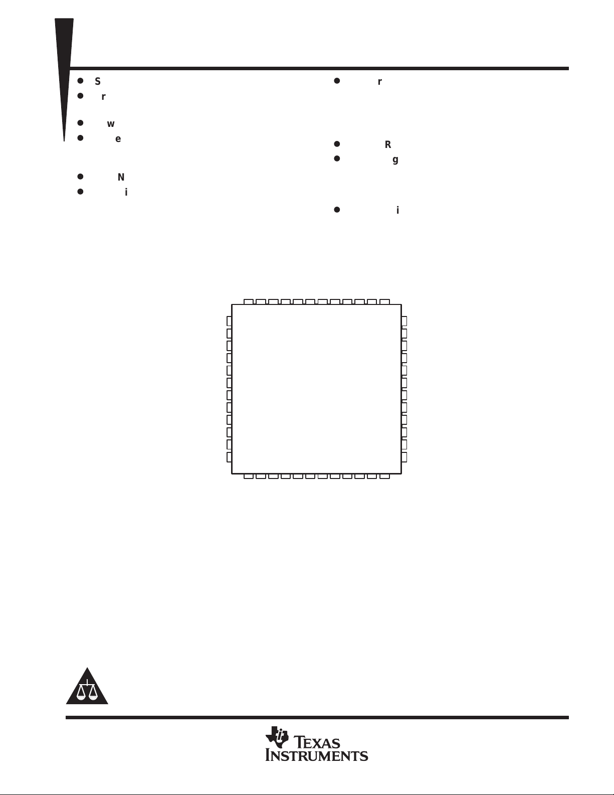
PT PACKAGE
(TOP VIEW)
NUNURXOUT
RXGAIN2
RX_TERM
TNETEL1400
EtherLoop TRANSCEIVER
SPHS004A – FEBRUARY 1999 – REVISED MARCH 1999
All Terminals Protected to Survive, Without
Damage, a Simulated Static Discharge of
1 kV From a 100-pF Capacitor Applied
Through a 1.5-kΩ Resistor With Respect to
Chip Ground (VEE)
Single-Rail 5-V Power Supply
Operating Temperature –40°C to 85°C
Ambient
– Allows Operation in Central Office and
Distributed-Server Modem Applications
48-Pin Thin Plastic Quad Flatpack
RXGAIN0
EE
RXGAIN1
TX_EN
V
V
37
EE
NU
38
RXIP
RXIN
V
REMN
TXOP
TXON
REMP
NU – Not used
V
V
NU
EE
CC
EE
39
40
41
42
43
44
45
46
47
48
3635343332313029282726
123
EE
V
CBIAS1
REMREF
45678
IP_INT
IN_INT
OP_INT
ON_INT
9
NU
TXINP
101112
NU
V
TXINN
25
24
23
22
21
20
19
18
17
16
15
14
13
EE
V
EE
TXGAIN3
TXGAIN2
TXGAIN1
TXGAIN0
ANG
REFP
RXBIAS
TXBIAS
V
CC
V
EE
V
EE
description
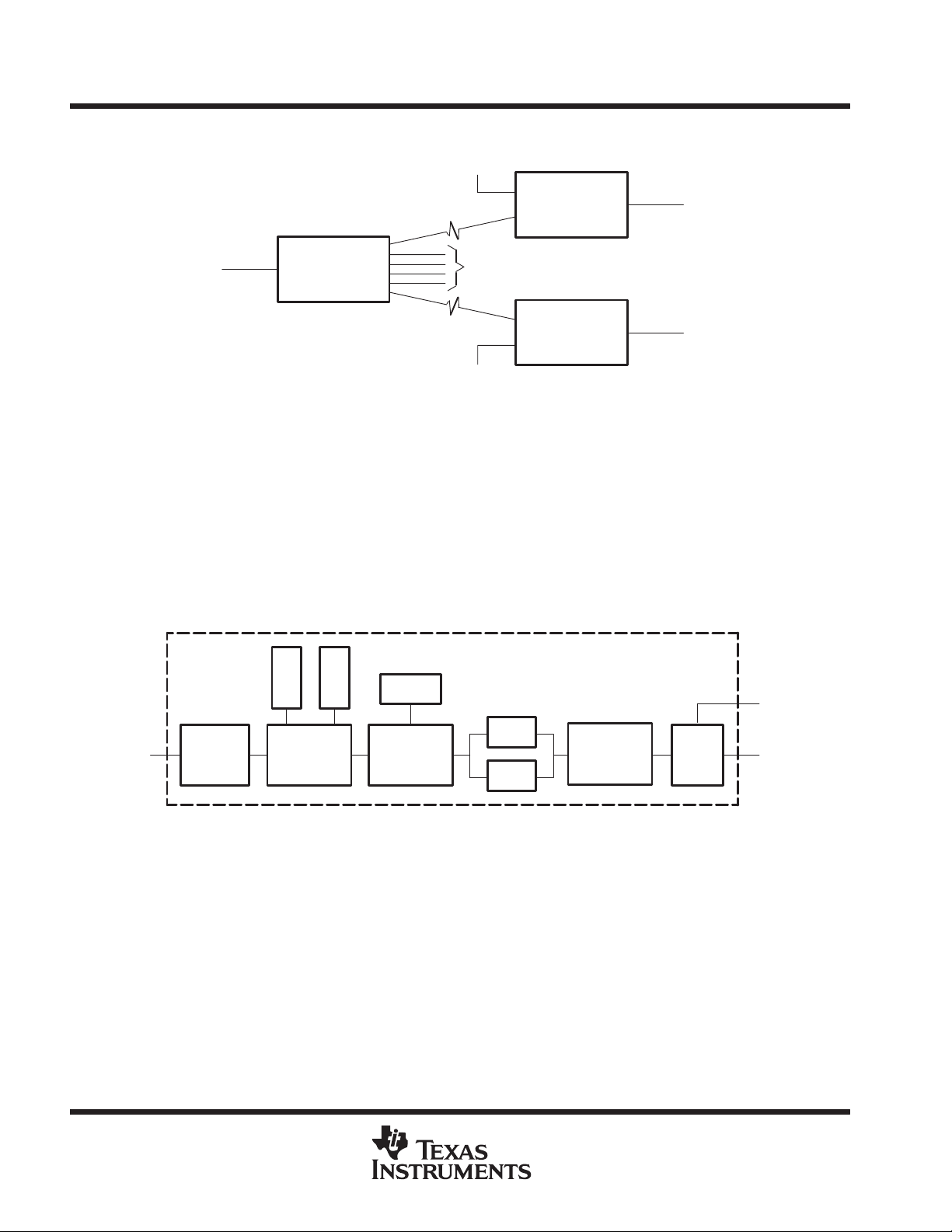
The TNETEL1400 is an Etherloop transceiver. EtherLoop technology enables simultaneous voice and Ethernet
communication over local-loop plain old telephone service (POTS) wiring. The TNETEL1400 supports data
rates of up to 6 Mbit/s and POTS wire lengths of up to 21,000 feet. Figure 1 shows a typical system with an
EtherLoop modem located at each end of the POTS line. Each EtherLoop modem has a 10Base-T Ethernet
interface and is responsible for buffering Ethernet data before sending it over the POTS wire. The server-end
(SE) EtherLoop modem is located in a central switching office and can communicate with several client-end
(CE) EtherLoop modems, based on a round-robin arbitration scheme. The CE EtherLoop modem typically is
located at a remote site.
PRODUCT PREVIEW
Please be aware that an important notice concerning availability, standard warranty, and use in critical applications of
Texas Instruments semiconductor products and disclaimers thereto appears at the end of this data sheet.
EtherLoop is a trademark of Elastic Networks.
PRODUCT PREVIEW information concerns products in the formative or
design phase of development. Characteristic data and other
specifications are design goals. Texas Instruments reserves the right to
change or discontinue these products without notice.
POST OFFICE BOX 655303 • DALLAS, TEXAS 75265
Copyright 1999, Texas Instruments Incorporated
1
TNETEL1400
g
EtherLoop TRANSCEIVER
SPHS004A – FEBRUARY 1999 – REVISED MARCH 1999
description (continued)
POTS Phone
☎
POTS
Line
Ethernet
Network
SE Modem
Central Office
See Note A
POTS
Line
POTS Phone
☎
NOTE A: Flexible multiplexin
Figure 2 shows a block diagram of a typical CE EtherLoop modem. Ethernet data destined for the POTS wire
is received via 10Base-T interface and presented to the EtherLoop processor. The EtherLoop processor
performs Ethernet frame processing and buffer management. The EtherLoop processor sends buffered
Ethernet frames to the TNETEL1200 EtherLoop modem. The TNETEL1200 performs data modulation before
passing the modulated digital data to a digital-to-analog (DAC) converter. The resulting analog signal passes
to the TNETEL1400 transceiver, which acts as the line interface. The modem uses a half-duplex communication
protocol over the POTS wire, and data received from the POTS wire follows the reverse path back to the
Ethernet framer.
scheme allows one SE modem to interface with many CE modems.
Figure 1. Typical EtherLoop System
CE Modem
Remote Location
CE Modem
Remote Location
Ethernet
Network
Ethernet
Network
ROM
FLASH
PRODUCT PREVIEW
Ethernet
Network
Figure 3 shows a block diagram of a typical SE EtherLoop modem. Data flow follows the same path as in the
CE EtherLoop modem. In the SE application, the EtherLoop processor also performs round-robin arbitration
between each of the attached TNETEL1400 devices.
Ethernet
Interface
EtherLoop
Processor
SDRAM
Figure 2. Typical CE EtherLoop Modem
SRAM
TNETEL1200
EtherLoop
Modem
DAC
ADC
TNETEL1400
EtherLoop
Transceiver
Voice
Band
Filter
☎
POTS
Line
POTS
Phone
2
POST OFFICE BOX 655303 • DALLAS, TEXAS 75265
TNETEL1400
EtherLoop TRANSCEIVER
SPHS004A – FEBRUARY 1999 – REVISED MARCH 1999
Ethernet
Network
Ethernet
Interface
ROM
FLASH
EtherLoop
Processor
SDRAM
SRAM
TNETEL1200
EtherLoop
Modem
Figure 3. Typical SE EtherLoop Modem
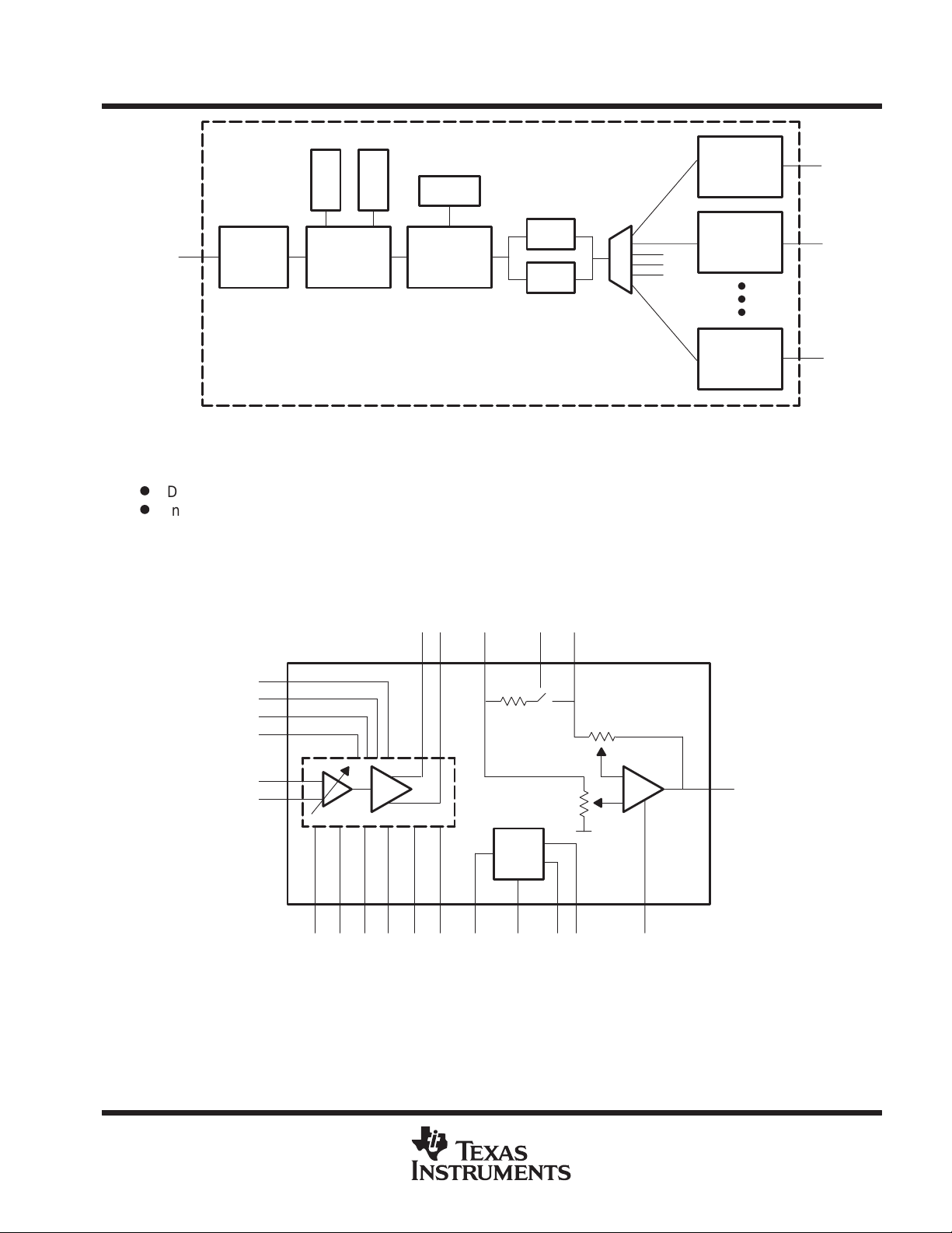
summary of TNETEL1400 EtherLoop transceiver
D
Drives POTS line with signal generated by DAC
D
Interfaces signal received from POTS line to ADC
functional block diagram
DAC
ADC
MUX
TNETEL1400
EtherLoop
Transceiver
TNETEL1400
EtherLoop
Transceiver
TNETEL1400
EtherLoop
Transceiver
POTS
Line
POTS
Line
POTS
Line
IP_INT
OP_INT
IN_INT
ON_INT
TXINN
TXINP
TX
REMP
TX_EN
REMREF
TXGAIN3–TXGAIN0
REMN
TXOP
TXON
CBIAS1
RXIP
Bias
TXBIAS
RX_TERM
REFP
RXIN
ANG
RXBIAS
RX
RXGAIN2–RXGAIN0
PRODUCT PREVIEW
RXOUT
POST OFFICE BOX 655303 • DALLAS, TEXAS 75265
3
TNETEL1400
T
EtherLoop TRANSCEIVER
SPHS004A – FEBRUARY 1999 – REVISED MARCH 1999
TX_IN
0.1 µF
0.1 µF
0.22 µF
TXINN
IP_INT
OP_INT
IN_INT
ON_INT
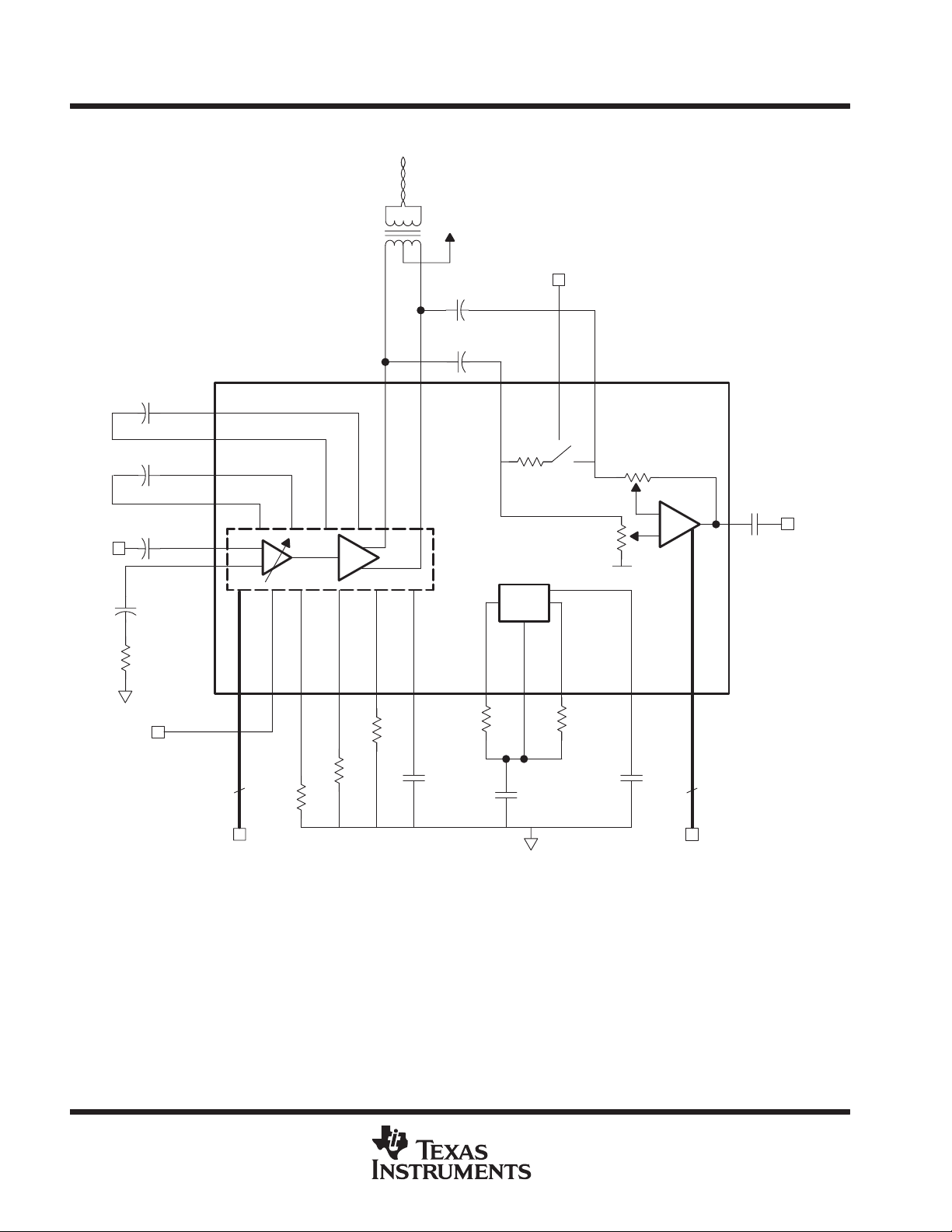
APPLICATION INFORMATION
5 V
RX_MODE
2.2 µF
2.2 µF
TXOP
TXON
RXIP
RXTERM
†
RXIN
0.22 µF
RX_OU
TXINP
0.22 µF
10 K
REMREF
PRODUCT PREVIEW
TX_EN
13 Ω
1%
TXGAIN
REMP
5 Ω
REMN
5 Ω
CBIAS1
4.99 kΩ 4.99 kΩ
100 nF
Bias
TXBIAS
RFEP
100 nF
RXBIAS
100 nF
ANG
34
RXGAIN
Figure 4. EtherLoop Front-End Application (CE)
†
All bias resistors should be 1% tolerance. The resistors on REMP, REMN, and REMREF also should be 1% and placed as close as possible
to their respective pins.
4
POST OFFICE BOX 655303 • DALLAS, TEXAS 75265

I/O
†
DESCRIPTION
EtherLoop TRANSCEIVER
SPHS004A – FEBRUARY 1999 – REVISED MARCH 1999
Terminal Functions
transmit (TX)
TERMINAL
NAME NO.
CBIAS1 2 I/O Transmit voltage bias decoupling
IN_INT 6 I Transmit interstage ac coupling pin 1 (negative side)
IP_INT 4 I Transmit interstage ac coupling pin 2 (positive side)
ON_INT 7 O Transmit interstage ac coupling pin 2 (negative side)
OP_INT 5 O Transmit interstage ac coupling pin 1 (positive side)
REMREF 3 O Transmit temperature-compensating bias reference
Transmit enable
TX_EN 26 I
TXBIAS 16 I Transmit current bias
TXGAIN3
TXGAIN2
TXGAIN1
TXGAIN0
TXINN 10 I Transmit input negative. TXINN can be coupled to ground for SE input).
TXINP 9 I Transmit input positive. TXINP can be coupled to ground for SE input).
TXON 46 O Transmitter output negative
TXOP 45 O Transmitter output positive
†
I = input, O = output
23 (MSB)
22
21
20 (LSB)
I
1 = Transmitter enabled
0 = Transmitter disabled
Transmit preattenuation select (0 to –30 dB in –3-dB steps)
0000 = 0 dB
0001 = – 3 dB
•
•
•
1010 = –30 dB
1011 = TX OFF
•
•
•
1110 = TX OFF
1111 = TX OFF
TNETEL1400
PRODUCT PREVIEW
POST OFFICE BOX 655303 • DALLAS, TEXAS 75265
5

TNETEL1400
I/O
†
DESCRIPTION
I/O
†
DESCRIPTION
DESCRIPTION
EtherLoop TRANSCEIVER
SPHS004A – FEBRUARY 1999 – REVISED MARCH 1999
Terminal Functions (Continued)
receive (RX)
TERMINAL
NAME NO.
Receive passive termination
RX_TERM 30 I
RXBIAS 17 I Receive current bias
RXGAIN2
RXGAIN1
RXGAIN0
RXIN 40 I Receiver input negative/TX feedback
RXIP 39 I Receiver input positive/TX feedback
RXOUT 31 O Receiver output (single ended)
†
I = input, O = output
29 (MSB)
27
28 (LSB)
I
RX_TERM = 1: 110 Ω switched IN
RX_TERM = 0: 110 Ω switched OUT
Receive gain select
000 = RX OFF
•
•
•
011 = RX OFF
100 = 0 dB
101 = 12 dB
110 = 24 dB
111 = 30 dB
miscellaneous
TERMINAL
NAME NO.
ANG 19 O Analog ground (2.5 V) reference
REFP 18 O 4-V bandgap reference
REMN 44 I/O Negative external emitter resistor
REMP 47 I/O Positive external emitter resistor
†
I = input, O = output
PRODUCT PREVIEW
power supply
TERMINAL
NAME NO.
NU 8, 11, 32, 33, 38, 41 Not used
V
CC
V
1, 12, 13, 14, 24, 25, 35, 36, 37, 42, 48 Ground
EE
15, 34, 43 5-V power
6
POST OFFICE BOX 655303 • DALLAS, TEXAS 75265

TNETEL1400
EtherLoop TRANSCEIVER
SPHS004A – FEBRUARY 1999 – REVISED MARCH 1999
absolute maximum ratings over operating free-air temperature (unless otherwise noted)
†
Supply-voltage range, VCC 4.3 V to VCC to 0.7 V. . . . . . . . . . . . . . . . . . . . . . . . . . . . . . . . . . . . . . . . . . . . . . . . . . .
Input-voltage range: Analog inputs –0.7 V to VCC to 0.7 V. . . . . . . . . . . . . . . . . . . . . . . . . . . . . . . . . . . . . . . . . . .
Output-voltage range, V
Storage temperature range, T
†
Stresses beyond those listed under “absolute maximum ratings” may cause permanent damage to the device. These are stress ratings only, and
functional operation of the device at these or any other conditions beyond those indicated under “recommended operating conditions” is not
implied. Exposure to absolute-maximum-rated conditions for extended periods may affect device reliability.
. . . . . . . . . . . . . . . . . . . . . . . . . . . . . . . . . . . . . . . . . . . . . . . . . . . . . . . . . . . . . . . . . . . . . . .
O
-55°C to 25°C. . . . . . . . . . . . . . . . . . . . . . . . . . . . . . . . . . . . . . . . . . . . . . . . . . . . .
stg
recommended operating conditions
MIN MAX UNIT
V
V
V
I
I
T
OH
OL
Supply voltage 4.75 5.25 V
CC
High-level input voltage 2.1 V
IH
Low-level input voltage 1 V
IL
High-level input current mA
Low-level input current mA
Operating free-air temperature range –40 85 °C
A
POST OFFICE BOX 655303 • DALLAS, TEXAS 75265
PRODUCT PREVIEW
7

TNETEL1400
ICCSupply current
A
TX attentuator accuracy
(
)
()
V
1.2 V
sinusoid at f
500 kHz
[
dB
[out ut is measured at IN_INT and IP_INT
,
,
,
dBc
EtherLoop TRANSCEIVER
SPHS004A – FEBRUARY 1999 – REVISED MARCH 1999
electrical characteristics over recommended operating conditions
PARAMETER TEST CONDITIONS MIN TYP†MAX UNIT
pp
V
REF
V
ANG
I
REFP
I
ANG
†
All typical values are at VCC = 5 V, TA = 25°C (unless otherwise noted).
4-V reference voltage 3.88 4 4.12 V
2.5-V reference voltage 2.38 2.5 2.62 V
4-V reference current Source 1 mA
2.5-V reference current Source/sink 100 mA
transmitter (see Figure 5)
PARAMETER TEST CONDITIONS MIN TYP†MAX UNIT
VCC = 5 V, RL = 110 Ω,
TX maximum output level
relative to maximum output
TX attentuator accuracy
(relative to maximum output)
TX output level variation
over frequency
PRODUCT PREVIEW
TX output
distortion
(all gain
settings)
TX output
signal-to-noise ratio (SNR)
(all gain settings)
TX maximum
output-level variation with V
Z
in(TXIN)
TX input impedance variation
as percent of Z
†
All typical values are at VCC = 5 V, TA = 25°C (unless otherwise noted).
NOTE 1: While the RX circuit is disabled during transmission, it is still connected and, therefore, must withstand the signal levels placed at its
Odd harmonics
Even harmonics
CC
TX
input impedance
in(TXIN)
input terminals.
RX_TERM = 0, TX_EN = 1,
V
(see Note 1)
VCC = 5 V, RL = 110 Ω,
RX_TERM = 0, TX_EN = 1, RXGAIN = 0XX,
output is measured at IN_INT and IP_INT
(ac coupled)]
30 kHz < f < 2.5 MHz
monotonically decreasing for f > 3 MHz,
RL = 110 Ω, RX_TERM = 0, TX_EN = 1,
V
with transformer connected as in Figure 1
(see Note 1)
VCC = 5 V, RL = 110 Ω,
RX_TERM = 0, TX_EN = 1,
V
(see Note 1)
VCC = 5 V, RL = 110 Ω,
RX_TERM = 0, TX_EN = 1,
V
(see Note 1)
VCC = 5 V ± 0.25 V, RL = 110 Ω,
RX_TERM = 0, TX_EN = 1,
V
(see Note 1)
TXGAIN = 0000, RXGAIN = 0XX (see Note 1) 1400
TXGAIN = 0000, RXGAIN = 0XX –30% 30%
= 1.2 VPP sinusoid at f = 500 kHz
(TXINP)
=
(TXINP)
= 1.2 VPP sinusoid at f = 500 kHz
(TXINP)
_
= 1.2 VPP sinusoid at f = 500 kHz
(TXINP)
= 1.2 VPP sinusoid at f = 500 kHz
(TXINP)
= 1.2 VPP sinusoid at f = 500 kHz
(TXINP)
PP
_
Normal operation 25 50
Power-down mode 1.5 3
=
TXGAIN = 0000,
RXGAIN = 0XX
TXGAIN = 0001 –3.3 –3 –2.7
TXGAIN = 0010 –6.3 –6 –5.7
TXGAIN = 0011 –9.3 –9 –8.7
TXGAIN = 0100 –12.3 –12 –11.7
TXGAIN = 0101 –15.3 –15 –14.7
TXGAIN = 0110 –18.3 –18 –17.7
TXGAIN = 0111 –21.3 –21 –20.7
TXGAIN = 1000 –24.3 –24 –23.7
TXGAIN = 1001 –27.3 –27 –26.7
TXGAIN = 1010 –30.3 –30 –29.7
TXGAIN = 0000,
RXGAIN = 0XX
TXGAIN = 0000,
RXGAIN = 0XX
TXGAIN = 0000,
RXGAIN = 0XX
TXGAIN = 0000,
RXGAIN = 0XX
21 22 23 dBm
–35
–50
50 dB
TYP+
30%
1 dB
1 dB/V
µ
Ω
8
POST OFFICE BOX 655303 • DALLAS, TEXAS 75265

TX supply current
mA
R
L
C
L
kHz < f < 2.75 MHz
RX idle channel noise
,
,
µ
RX gain accurac
30 kH
TERM
500
dB
V
(RXIP
RXIN)
V
PP
sinusoid at f = 500 kHz
TNETEL1400
EtherLoop TRANSCEIVER
SPHS004A – FEBRUARY 1999 – REVISED MARCH 1999
transmitter (see Figure 5) (continued)
PARAMETER TEST CONDITIONS MIN TYP†MAX UNIT
I
rms(TXOP)
I
rms(TXON)
TX output stability
TX output return loss TXGAIN = 0000, RXGAIN = 0XX 18 dB
TX power-up time TXGAIN = 0000, RXGAIN = 0XX (see Note 2) 100 µs
†
All typical values are at VCC = 5 V, TA = 25°C (unless otherwise noted).
NOTES: 1. While the RX circuit is disabled during transmission, it is still connected and, therefore, must withstand the signal levels placed at
–
TX output
current balance
pp
its input terminals.
2. The power-up/power-down time is the time it takes for the signal path to completely settle and meet all the transmission specifications
after TXGAIN and RXGAIN are set to power-up condition or switched from one gain setting to another. This time consists of slewing
and exponential settling of bias and AC coupling capacitors and, therefore, the values of these components must be as shown in
the application diagram, Figure 4.
VCC = 5 V, RL = 110 Ω,
RX_TERM = 0, TX_EN = 1,
V
(see Note 1)
Source impedance ≤ 50 Ω,
Supply impedance ≤ 10 Ω,
Z
and open circuit
V
V
= 1.2 VPP sinusoid at f = 500 kHz
(TXINP)
: voltage standing-wave ratio (VSWR) 4:1
loads
= 0, TXGAIN = 0000 35 45
OUT
= MAX, TXGAIN = 0000 120
OUT
TXGAIN = 0000,
RXGAIN = 0XX
TXGAIN = 0000,
RXGAIN = 0XX
–5 5 mA
receiver (see Figures 6 and 7)
PARAMETER TEST CONDITIONS MIN TYP†MAX UNIT
= 2 kΩ,
RX_TERM = 1, TX_EN = 0,
_
V
(RXIP – RXIN)
(see Note 3)
y
RX gain over frequency
(WRT gain at 500 kHz)
RX power-supply
rejection
(WRT VCC only)
RX common-mode
rejection
RX IIP3 intercept
†
All typical values are at VCC = 5 V, TA = 25°C (unless otherwise noted).
NOTES: 3. Idle channel noise is the noise (V
2.75-MHz band. This specification is in place of the original noise-figure specification, and is correlated to NF with laboratory
measurements.
4. The two tones used for this test are at 1.39 MHz and 1.58 MHz, and the in-band IIP3 products are at 1.2 MHz and 1.77 MHz. The
IIP3 intercept point is the output power level, where the power of the harmonics equals that of the signal frequencies. This point is
an intersection of two straight lines extrapolated from two low-power measurements.
VCC = 5 V, RL = 2 kΩ, CL = 20 pF,
z < f < 2.75 MHz, RX_
V
–
–
RL = 2 kΩ, CL = 20 pF, 30 kHz < f < 2.75 MHz,
30 kHz < f < 2.5 MHz monotically decreasing
for f > 3 MHz, TX_EN = 0,
V
(RXIP – RXIN)
RL = 2 kΩ, CL = 20 pF, dc < f < 3 MHz, TX_EN = 0,
V
(RXIP – RXIN)
RL = 2 kΩ, CL = 20 pF, TX_EN = 0, V
V
(RXIP – RXIN)
RL = 2 kΩ, CL = 20 pF, TX_EN = 0,
V
(RXIP – RXIN)
(see Note 4)
p
= 20 F, 30
_
= 0.04 VPP sinusoid at f = 500 kHz
= 0.04 V
= 0.04
= 0.04 VPP sinusoid at f = 500 kHz
= 0.04 VPP sinusoid at f = 500 kHz
= 0.04 VPP sinusoid at f = 500 kHz
= 0.04 VPP sinusoid at f = 500 kHz
) measured at RXOUT with no signal at RXIN. This voltage is integrated over the 30-KHz to
rms
= 1, TX_EN = 0,
sinusoid at f =
(RXIN)
,
kHz
= 1.5 VPP,
RXGAIN = 11 691
RXGAIN = 10 478
RXGAIN = 01 266
RXGAIN = 00 160
RXGAIN = 11 24 30 31
RXGAIN = 10 23 24 25
RXGAIN = 01 11 12 13
RXGAIN = 00 –1 0 1
RX_TERM = 1,
RXGAIN = 111
RX_TERM = 1,
RXGAIN = 111
RX_TERM = 1,
RXGAIN = 111
RX_TERM = 1,
RXGAIN = 111
–1 1 dB
30 dB
17 dBm
µV
RMS
PRODUCT PREVIEW
0.03 V/V
POST OFFICE BOX 655303 • DALLAS, TEXAS 75265
9

TNETEL1400
RX Z
L
,
L
,,_,
EtherLoop TRANSCEIVER
SPHS004A – FEBRUARY 1999 – REVISED MARCH 1999
receiver (see Figures 6 and 7) (continued)
PARAMETER TEST CONDITIONS MIN TYP†MAX UNIT
RX output total
harmonic distortion
IN
RX maximum
supply current
RX power-up time
Power-down
supply current
†
All typical values are at VCC = 5 V, TA = 25°C (unless otherwise noted).
NOTE 2. The power-up/power-down time is the time it takes for the signal path to completely settle and meet all the transmission specifications
after TXGAIN and RXGAIN are set to power-up condition or switched from one gain setting to another. This time consists of slewing
and exponential settling of bias and AC coupling capacitors and, therefore, the values of these components must be as shown in the
application diagram, Figure 4.
RL = 2 kΩ, CL = 20 pF, TX_EN = 0, V
V
(RXIP – RXIN)
R
= 2 kΩ, C
V
(RXIP – RXIN)
RL = 2 kΩ, CL = 20 pF, TX_EN = 0, V
V
(RXIP – RXIN)
RL = 2 kΩ, CL = 20 pF, TX_EN = 0,
V
(RXIP – RXIN)
(see Note 2)
RL = 2 kΩ, CL = 20 pF, RX_TERM = 1, TX_EN = 0,
V
(RXIP – RXIN)
(see Note 2)
= 0.04 VPP sinusoid at f = 500 kHz
= 20 pF, RXGAIN = 11 1, TX_EN = 0,
= 0.04 VPP sinusoid at f = 500 kHz
= 0.04 VPP sinusoid at f = 500 kHz
= 0.04 VPP sinusoid at f = 500 kHz
= 0.04 VPP sinusoid at f = 500 kHz
(RXOUT)
(RXOUT)
= 2 VPP,
= 4 VPP,
RX_TERM = 1,
RXGAIN = 111
RX_TERM = 1 77 110 143 Ω
RX_TERM = 0 10 kΩ
RX_TERM = 1,
RXGAIN = 111
RX_TERM = 1,
RXGAIN = 111
TXGAIN = 1111,
RXGAIN = 000
–40 dBc
20 mA
30 µs
3 mA
PRODUCT PREVIEW
10
POST OFFICE BOX 655303 • DALLAS, TEXAS 75265

TNETEL1400
EtherLoop TRANSCEIVER
SPHS004A – FEBRUARY 1999 – REVISED MARCH 1999
110 V
5 V
RX_TERM
1 µF
1 µF
33 nF
33 nF
33 nF
+
V
I
33 nF
–
5 Ω
5 Ω
4
7.5 Ω
4.99 kΩ 80.6 kΩ
100 nF
Bias
3
100 nF
100 nF
PRODUCT PREVIEW
[000]
TXGAIN
Figure 5. TX Test Circuit
RXGAIN
POST OFFICE BOX 655303 • DALLAS, TEXAS 75265
11

TNETEL1400
EtherLoop TRANSCEIVER
SPHS004A – FEBRUARY 1999 – REVISED MARCH 1999
33 nF
33 nF
0.04 V
PP
–
1 µF1 µF
Bias
+
100 nF
2 kΩ
5 Ω
5 Ω
4 3
7.5 Ω
PRODUCT PREVIEW
4.99 kΩ 80.6 kΩ
100 nF
100 nF
100 nF
Figure 6. RX Test Circuit
RXGAIN[1111]
12
POST OFFICE BOX 655303 • DALLAS, TEXAS 75265

TNETEL1400
EtherLoop TRANSCEIVER
SPHS004A – FEBRUARY 1999 – REVISED MARCH 1999
110 Ω
33 nF
33 nF
1 µF
Bias
5 Ω
5 Ω
4 3
7.5 Ω
4.99 kΩ 80.6 kΩ
100 nF
100 nF
1 µF
100 nF
Figure 7. RX Noise Test Circuit
RXGAIN[1111]
PRODUCT PREVIEW
POST OFFICE BOX 655303 • DALLAS, TEXAS 75265
13

TNETEL1400
EtherLoop TRANSCEIVER
SPHS004A – FEBRUARY 1999 – REVISED MARCH 1999
MECHANICAL DATA
PT (S-PQFP-G48) PLASTIC QUAD FLA TPACK
37
48
0,50
1,45
1,35
36
0,27
0,17
25
24
13
1
5,50 TYP
7,20
SQ
6,80
9,20
SQ
8,80
12
0,08
M
0,05 MIN
0,13 NOM
Gage Plane
0,25
0°–7°
PRODUCT PREVIEW
1,60 MAX
NOTES: A. All linear dimensions are in millimeters.
B. This drawing is subject to change without notice.
C. Falls within JEDEC MS-026
D. This may also be a thermally enhanced plastic package with leads conected to the die pads.
Seating Plane
0,10
0,75
0,45
4040052/C 11/96
14
POST OFFICE BOX 655303 • DALLAS, TEXAS 75265

IMPORTANT NOTICE
T exas Instruments and its subsidiaries (TI) reserve the right to make changes to their products or to discontinue
any product or service without notice, and advise customers to obtain the latest version of relevant information
to verify, before placing orders, that information being relied on is current and complete. All products are sold
subject to the terms and conditions of sale supplied at the time of order acknowledgement, including those
pertaining to warranty, patent infringement, and limitation of liability.
TI warrants performance of its semiconductor products to the specifications applicable at the time of sale in
accordance with TI’s standard warranty. Testing and other quality control techniques are utilized to the extent
TI deems necessary to support this warranty . Specific testing of all parameters of each device is not necessarily
performed, except those mandated by government requirements.
CERTAIN APPLICATIONS USING SEMICONDUCTOR PRODUCTS MAY INVOLVE POTENTIAL RISKS OF
DEATH, PERSONAL INJURY, OR SEVERE PROPERTY OR ENVIRONMENTAL DAMAGE (“CRITICAL
APPLICATIONS”). TI SEMICONDUCTOR PRODUCTS ARE NOT DESIGNED, AUTHORIZED, OR
WARRANTED TO BE SUITABLE FOR USE IN LIFE-SUPPORT DEVICES OR SYSTEMS OR OTHER
CRITICAL APPLICA TIONS. INCLUSION OF TI PRODUCTS IN SUCH APPLICATIONS IS UNDERST OOD TO
BE FULLY AT THE CUSTOMER’S RISK.
In order to minimize risks associated with the customer’s applications, adequate design and operating
safeguards must be provided by the customer to minimize inherent or procedural hazards.
TI assumes no liability for applications assistance or customer product design. TI does not warrant or represent
that any license, either express or implied, is granted under any patent right, copyright, mask work right, or other
intellectual property right of TI covering or relating to any combination, machine, or process in which such
semiconductor products or services might be or are used. TI’s publication of information regarding any third
party’s products or services does not constitute TI’s approval, warranty or endorsement thereof.
Copyright 1999, Texas Instruments Incorporated
 Loading...