


www.DataSheet4U.com
www.ti.com
TMS320DM647/TMS320DM648
1 TMS320DM647/TMS320DM648 Digital Media Processor
1.1 Features
• High-Performance Digital Media Processor • C64x+ L1/L2 Memory Architecture
(DM647/DM648)
– 720, 900-MHz C64x+™ Clock Rate [Direct Mapped]
– 1.39, 1.11-ns Instruction Cycle Time – 256K-bit (32K-byte) L1D Data Cache
– 5760, 7200 MIPS
– Eight 32-Bit C64x+ Instructions/Cycle
– Fully Software-Compatible With
C64x/Debug
– Commercial Temperature Ranges
• VelociTI.2™ Extensions to VelociTI™
Advanced Very-Long-Instruction-Word (VLIW)
TMS320C64x+™ DSP Core
– Eight Highly Independent Functional Units
With VelociTI.2 Extensions:
• Six ALUs (32-/40-Bit), Each Supports
Single 32-bit, Dual 16-bit, or Quad 8-bit
Arithmetic per Clock Cycle
• Two Multipliers Support Four 16 x 16-bit
Multiplies (32-bit Results) per Clock
Cycle or Eight 8 x 8-bit Multiplies (16-Bit
Results) per Clock Cycle
– Load-Store Architecture With Non-Aligned
Support
– 64 32-bit General-Purpose Registers
– Instruction Packing Reduces Code Size
– All Instructions Conditional
– Additional C64x+™ Enhancements
• Protected Mode Operation
• Exceptions Support for Error Detection
and Program Redirection
• Hardware Support for Modulo Loop
Auto-Focus Module Operation
• C64x+ Instruction Set Features
– Byte-Addressable (8-/16-/32-/64-bit Data)
– 8-bit Overflow Protection
– Bit-Field Extract, Set, Clear
– Normalization, Saturation, Bit-Counting
– VelociTI.2 Increased Orthogonality
– C64x+ Extensions • Multichannel Audio Serial Port (McASP)
• Compact 16-bit Instructions – Ten Serializers and SPDIF (DIT) Mode
• Additional Instructions to Support
Complex Multiplies
– 256K-bit (32K-byte) L1P Program Cache
[2-Way Set-Associative]
– 2M-bit/256K-byte (DM647) or
4M-Bit/512K-byte) (DM648) L2 Unified
Mapped RAM/Cache [Flexible Allocation]
• Supports Little Endian Mode Only
• Five Configurable Video Ports
– Providing a Glueless I/F to Common Video
Decoder and Encoder Devices
– Supports Multiple Resolutions/Video Stds
• VCXO Interpolated Control Port (VIC)
– Supports Audio/Video Synchronization
• External Memory Interfaces (EMIFs)
– 32-Bit DDR2 SDRAM Memory Controller
With 256M-Byte Address Space (1.8-V I/O)
– Asynchronous 16-Bit Wide EMIF (EMIFA)
With up to 64M-Byte Address Reach
– Glueless Interface to Asynchronous
Memories (SRAM, Flash, and EEPROM)
– Synchronous Memories (SBSRAM and ZBT
SRAM)
– Supports Interface to Standard Sync
Devices and Custom Logic (FPGA, CPLD,
ASICs, etc)
• Enhanced Direct-Memory-Access (EDMA)
Controller (64 Independent Channels)
• 3-Port Gigabit Ethernet Switch
• Four 64-Bit General-Purpose Timers (Each
Configurable as Two 32-Bit Timers)
• One UART (With RTS and CTS Flow Control)
• One 4-wire Serial Port Interface (SPI) With Two
Chip-Selects
• Master/Slave Inter-Integrated Circuit (I2C
Bus™)
• 16/32-Bit Host-Port Interface (HPI)
• 32-Bit 33-/66-MHz, 3.3-V Peripheral Component
Interconnect (PCI) Master/Slave Interface
Conforms to PCI Specification 2.3
• VLYNQ™ Interface (FPGA Interface)
• On-Chip ROM Bootloader
Digital Media Processor
SPRS372 – MAY 2007
Please be aware that an important notice concerning availability, standard warranty, and use in critical applications of Texas
Instruments semiconductor products and disclaimers thereto appears at the end of this document.
PRODUCT PREVIEW information concerns products in the
formative or design phase of development. Characteristic data and
other specifications are design goals. Texas Instruments reserves
the right to change or discontinue these products without notice.
Copyright © 2007, Texas Instruments Incorporated

www.ti.com
PRODUCT PREVIEW
TMS320DM647/TMS320DM648
Digital Media Processor
SPRS372 – MAY 2007
• Individual Power-Saving Modes – 529-pin nFBGA (ZUT suffix)
• Flexible PLL Clock Generators
• IEEE-1149.1 (JTAG™)
Boundary-Scan-Compatible
• 32 General-Purpose I/O (GPIO) Pins
(Multiplexed With Other Device Functions)
• Package:
1.1.1 Trademarks
TMS320C64x+, C64x, C64x+, VelociTI, VelociTI.2, VLYNQ, TMS320C6000, C6000, TI, and TMS320 are
trademarks of Texas Instruments.
I2C Bus is a registered trademark of Koninklijke Philips Electronics N.V.
Windows is a registered trademark of Microsoft Corporation in the United States and/or other countries.
All trademarks are the property of their respective owners.
1.2 Description
The TMS320C64x+™ DSPs (including the TMS320DM647/TMS320DM648 devices) are the
highest-performance fixed-point DSP generation in the TMS320C6000™ DSP platform. The
DM647/DM648 devices are based on the third-generation high-performance, advanced VelociTI™
very-long-instruction-word (VLIW) architecture developed by Texas Instruments (TI), making these DSPs
an excellent choice for digital media applications. The C64x+™ devices are upward code-compatible from
previous devices that are part of the C6000™ DSP platform. The C64x™ DSPs support added
functionality and have an expanded instruction set from previous devices.
– 19x19 mm 0.8 mm pitch BGA
– 0.09- µ m/6-Level Cu Metal Process (CMOS)
• 3.3-V and 1.8-V I/O, 1.2-V Internal (-720, -900)
• Applications:
– Digital Video Recording
Any reference to the C64x DSP or C64x CPU also applies, unless otherwise noted, to the C64x+ DSP and
C64x+ CPU, respectively.
With performance of up to 7200 million instructions per second (MIPS) at a clock rate of 900 MHz, the
C64x+ core offers solutions to high-performance DSP programming challenges. The DSP core possesses
the operational flexibility of high-speed controllers and the numerical capability of array processors. The
C64x+ DSP core processor has 64 general-purpose registers of 32-bit word length and eight highly
independent functional units—two multipliers for a 32-bit result and six arithmetic logic units (ALUs). The
eight functional units include instructions to accelerate the performance in video and imaging applications.
The DSP core can produce four 16-bit multiply-accumulates (MACs) per cycle for a total of 2400 million
MACs per second (MMACS), or eight 8-bit MACs per cycle for a total of 4800 MMACS. For more details
on the C64x+ DSP, see the TMS320C64x/C64x+ DSP CPU and Instruction Set Reference Guide
(literature number SPRU732 ).
The DM647/DM648 devices also have application-specific hardware logic, on-chip memory, and additional
on-chip peripherals similar to the other C6000 DSP platform devices. The DM647/DM648 core uses a
two-level cache-based architecture. The Level 1 program cache (L1P) is a 256K-bit direct mapped cache
and the Level 1 data cache (L1D) is a 256K-bit 2-way set-associative cache. The Level 2 memory/cache
(L2) consists of a 4M-bit (DM648) or 2M-bit (DM647) memory space that is shared between program and
data space. L2 memory can be configured as mapped memory, cache, or combinations of the two.
The peripheral set includes: The DM647/DM648 devices have five configurable 16-bit video port
peripherals (VP0, VP1, VP2, VP3, and VP4). These video port peripherals provide a glueless interface to
common video decoder and encoder devices. The DM647/DM648 video port peripherals support multiple
resolutions and video standards (e.g., CCIR601, ITU-BT.656, BT.1120, SMPTE 125M, 260M, 274M, and
296M), a VCXO interpolated control port (VIC); a 1000 Mbps 3-port switch with a management data
input/output (MDIO) module and two SGMII ports (DM648 only); an 1000 Mbps Ethernet media access
controller (EMAC) and a management data input/output (MDIO) module (only DM647); a 4-bit transmit,
TMS320DM647/TMS320DM648 Digital Media Processor2 Submit Documentation Feedback

www.ti.com
TMS320DM647/TMS320DM648
Digital Media Processor
SPRS372 – MAY 2007
4-bit receive VLYNQ interface; an inter-integrated circuit (I2C) bus interface; a multichannel audio serial
port (McASP) with ten serializers; four 64-bit general-purpose timers each configurable as two
independent 32-bit timers; a user-configurable 16-bit or 32-bit host-port interface (HPI); 32 pins for
general-purpose input/output (GPIO) with programmable interrupt/event generation modes, multiplexed
with other peripherals; one UART; and two glueless external memory interfaces: a synchronous and
asynchronous external memory interface (EMIFA) for slower memories/peripherals, and a higher DDR2
SDRAM interface.
The video port peripherals provide a glueless interface to common video decoder and encoder devices.
The video port peripherals support multiple resolutions and video standards (e.g., CCIR601, ITU-BT.656,
BT.1120, SMPTE 125M, 260M, 274M, and 296M).
The video port peripherals are configurable and can support either video capture and/or video display
modes. Each video port consists of two channels (A and B) with a 5120-byte capture/display buffer that is
splittable between the two channels.
For more details on the video port peripherals, see the TMS320C64x DSP Video Port/VCXO Interpolated
Control (VIC) Port Reference Guide (literature number SPRU629).
The management data input/output (MDIO) module continuously polls all 32 MDIO addresses to
enumerate all PHY devices in the system.
The I2C and VLYNQ ports allow the device to easily control peripheral modules and/or communicate with
host processors.
The rich peripheral set provides the ability to control external peripheral devices and communicate with
external processors. For details on each of the peripherals, see the related sections later in this document
and the associated peripheral reference guides.
The DM647/DM648 devices have a complete set of development tools. These include C compilers, a DSP
assembly optimizer to simplify programming and scheduling, and a Windows™ debugger interface for
visibility into source code execution.
Submit Documentation Feedback TMS320DM647/TMS320DM648 Digital Media Processor 3

www.ti.com
PRODUCT PREVIEW
Timers
(464-bit
or832-bit)
EDMA 3.0
CC
TC TCTCTC
SwitchedCentralResource
or
PCI66
UHPI
3-portEthernet
Switch
Subsystem
SGMII
(x2,DM648)
(x1,DM647)
L1D 32KB
C64x+
Mega
L1P 32KB
L2 RAM
256KB
(DM647)
512KB
(DM648)
L2 ROM
64KB
ImagingCoprocessor
VLYNQ
DDR2
EMIFA 16-bit
VideoPorts(5)
UART
McASP
SPI
I2C
PLL
JTAG
GPIOx32
VIC
DM647/DM648
TMS320DM647/TMS320DM648
Digital Media Processor
SPRS372 – MAY 2007
1.3 Functional Block Diagram
Figure 1-1 shows the functional block diagram of the DM647/DM648 device.
TMS320DM647/TMS320DM648 Digital Media Processor4 Submit Documentation Feedback
Figure 1-1. TMS320DM647/TMS320DM648 Functional Block Diagram

www.ti.com
TMS320DM647/TMS320DM648
Digital Media Processor
SPRS372 – MAY 2007
Contents
1 TMS320DM647/TMS320DM648 Digital Media 6 Peripheral Information and Electrical
Processor .................................................. 1 Specifications ........................................... 56
1.1 Features .............................................. 1 6.1 Parameter Information .............................. 56
1.1.1 Trademarks .......................................... 2
1.2 Description ............................................ 2
1.3 Functional Block Diagram ............................ 4
2 Device Overview ......................................... 6
2.1 Device Characteristics ................................ 6
2.2 CPU (DSP Core) Description ......................... 7
2.3 C64x+ CPU .......................................... 10
2.4 Memory Map Summary ............................. 12
2.5 Pin Assignments .................................... 15
2.6 Terminal Functions .................................. 19
2.7 Device Support ...................................... 33
2.8 Device and Development-Support Tool
Nomenclature ....................................... 35
2.9 Documentation Support ............................. 36
3 Device Configuration .................................. 38
3.1 System Module Registers ........................... 38
3.2 Bootmode Registers ................................ 38
3.3 Debugging Considerations .......................... 47
3.4 Pullup/Pulldown Resistors ........................... 47
4 System Interconnect ................................... 49
4.1 Internal Buses, Bridges, and Switch Fabrics ........ 49
4.2 Data Switch Fabric Connections .................... 49
4.3 Configuration Switch Fabric ......................... 51
5 Device Operating Conditions ........................ 53
5.1 Absolute Maximum Ratings Over Operating
Temperature Range (Unless Otherwise Noted) ..... 53
5.2 Recommended Operating Conditions ............... 54
5.3 Electrical Characteristics Over Recommended
Ranges of Supply Voltage and Operating
Temperature (Unless Otherwise Noted) ............ 55
6.2 Recommended Clock and Control Signal Transition
Behavior ............................................. 58
6.3 Power Supplies ...................................... 58
6.4 PLL1 and PLL1 Controller ........................... 63
6.5 PLL2 and PLL2 Controller ........................... 67
6.6 Enhanced Direct Memory Access (EDMA3)
Controller ............................................ 70
6.7 Reset Controller ..................................... 83
6.8 Interrupts ............................................ 90
6.9 DDR2 Memory Controller ........................... 94
6.10 External Memory Interface A (EMIFA) .............. 96
6.11 Video Port .......................................... 104
6.12 VCXO Interpolated Control (VIC) .................. 112
6.13 Universal Asynchronous Receiver/Transmitter
(UART) ............................................. 114
6.14 Inter-Integrated Circuit (I2C) ....................... 116
6.15 Host-Port Interface (HPI) Peripheral ............... 120
6.16 Peripheral Component Interconnect (PCI) ......... 131
6.17 Multichannel Audio Serial Port (McASP)
Peripheral .......................................... 136
6.18 3-Port Ethernet Switch Subsystem (3PSW) ....... 144
6.19 Management Data Input/Output (MDIO) ........... 153
6.20 Timers .............................................. 155
6.21 VLYNQ Peripheral ................................. 157
6.22 General-Purpose Input/Output (GPIO) ............. 160
6.23 IEEE 1149.1 JTAG ................................. 163
7 Mechanical Data ....................................... 165
7.1 Thermal Data for ZUT .............................. 165
7.1.1 Packaging Information ............................. 165
Submit Documentation Feedback Contents 5
www.ti.com
PRODUCT PREVIEW
TMS320DM647/TMS320DM648
Digital Media Processor
SPRS372 – MAY 2007
2 Device Overview
2.1 Device Characteristics
Table 2-1 , provides an overview of the TMS320DM647/TMS320DM648 DSPs. The tables show significant
features of the DM647/DM648 devices, including the capacity of on-chip RAM, the peripherals, the CPU
frequency, and the package type with pin count.
Table 2-1. Characteristics of the DM647/DM648 Processor
HARDWARE FEATURES DM647 DM648
DDR2 memory controller (32-bit bus
width) [1.8 V I/O]
16-bit bus width
synchronous/asynchronous EMIF 1 1
[EMIFA]
EDMA3 (64 independent channels, 8
QDMA channels)
Timers (each configurable as 1 64-bit or 2 (each configurable as 1 64-bit or 2
Peripherals
Not all peripheral
pins are available
at the same time
(For more detail,
see Section 3 .)
On-Chip Memory
MegaModule Rev
ID
CPU ID + CPU
Rev ID
JTAG BSDL_ID 0x0B77 A02F 0x0B77 A02F
CPU Frequency MHz 720, 900 720, 900
Cycle Time ns 1.39 ns (-720), 1.11 ns (-900) 1.39 ns (-720), 1.11 ns (-900)
Voltage
PLL Options CLKIN1 frequency multiplier x1 (Bypass), x15, x20, x25, x30, x32 x1 (Bypass), x15, x20, x25, x30, x32
BGA Package 529-Pin Flip Chip Plastic BGA (ZUT) 529-Pin Flip Chip Plastic BGA (ZUT)
UART (with RTS and CTS flow control) (with RTS and CTS flow control)
I2C 1 (Master/Slave) 1 (Master/Slave)
SPI 1 (4-wire, 2 chip select) 1 (4-wire, 2 chip select)
McASP 1 (10 serailizers) 1 (10 serailizers)
3-port Ethernet Switch Subsystem
supporting 10/100/1000 Base-T 1 SGMII port available 2 SGMII ports available
Management data input/output (MDIO)
VLYNQ 1 1
General-purpose input/output port
(GPIO)
HPI (16/32-bit) 1 1
PCI (32 bit) (33 MHz or 66 MHz) 1 (PCI33 or PCI66) 1 (PCI33 or PCI66)
VIC 1 1
Configurable video ports 5 5
Size (bytes) 320KB RAM, 64KB ROM 576KB RAM, 64KB ROM
Organization to 32KB) 32KB)
Revision ID Register
(MM_REVID[15:0]) 0x0003 0x0003
(address location 0x0181 2000)
Control Status Register (CSR.[31:16]) 0x1000 0x1000
JTAGID register
(address location: 0x0204 9018)
Core (V) 1.2 V (-720, 900) 1.2 V (-720, 900)
I/O (V) 1.8 V, 3.3 V 1.8 V, 3.3 V
1 1
1 1
4 64-bit General Purpose 4 64-bit General Purpose
32-bit) 32-bit)
Up to 32 pins Up to 32 pins
32KB L1 program (L1P)/cache (Cache 32KB L1 program (L1P)/cache (up to
up to 32KB) 32KB)
32KB L1 data (L1D)/cache (Cache up 32KB L1 data (L1D)/cache (up to
256KB unified mapped RAM/Cache 512 KB unified mapped RAM/Cache
(L2) (L2)
64KB Boot ROM 64KB Boot ROM
Device Overview6 Submit Documentation Feedback

www.ti.com
TMS320DM647/TMS320DM648
Digital Media Processor
SPRS372 – MAY 2007
Table 2-1. Characteristics of the DM647/DM648 Processor (continued)
HARDWARE FEATURES DM647 DM648
Process 0.09- µ m/6-Level Cu Metal Process
Technology (CMOS)
Product Preview (PP), Advance
Product Status
(1) PRODUCT PREVIEW information concerns experimental products (designated as TMX) that are in the formative or design phase of
development. Characteristic data and other specifications are design goals. Texas Instruments reserves the right to change or
discontinue these products without notice.
(1)
Information (AI), PP PP
or Production Data (PD)
2.2 CPU (DSP Core) Description
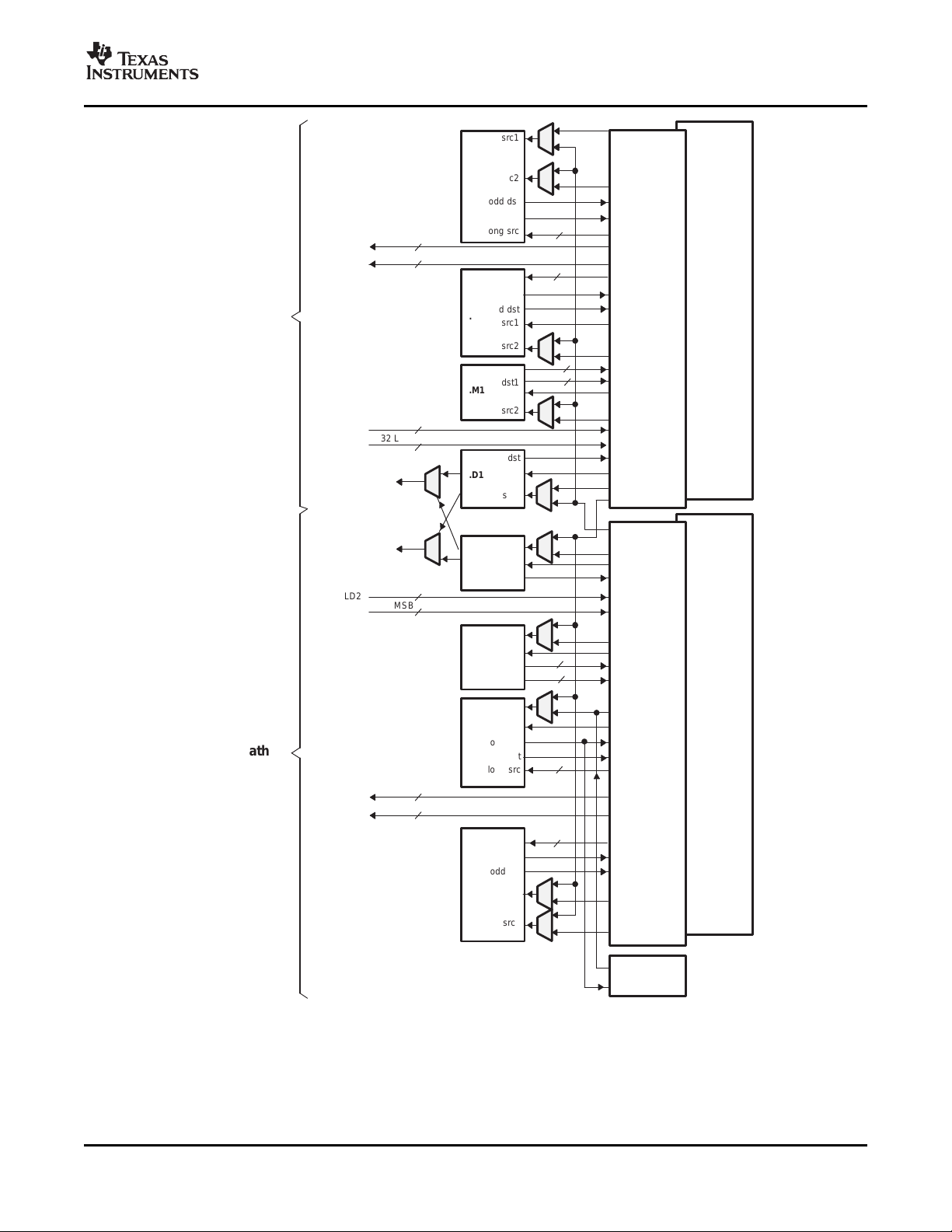
The C64x+ central processing unit (CPU) consists of eight functional units, two register files, and two data
paths as shown in Figure 2-1 . The two general-purpose register files (A and B) each contain 32 32-bit
registers for a total of 64 registers. The general-purpose registers can be used for data or can be data
address pointers. The data types supported include packed 8-bit data, packed 16-bit data, 32-bit data,
40-bit data, and 64-bit data. Values larger than 32 bits, such as 40-bit-long or 64-bit-long values are stored
in register pairs, with the 32 LSBs of data placed in an even register and the remaining 8 or 32 MSBs in
the next upper register (which is always an odd-numbered register).
The eight functional units (.M1, .L1, .D1, .S1, .M2, .L2, .D2, and .S2) are each capable of executing one
instruction every clock cycle. The .M functional units perform all multiply operations. The .S and .L units
perform a general set of arithmetic, logical, and branch functions. The .D units primarily load data from
memory to the register file and store results from the register file into memory.
0.09 µ m 0.09 µ m
The C64x+ CPU extends the performance of the C64x core through enhancements and new features.
Each C64x+ .M unit can perform one of the following each clock cycle: one 32 x 32 bit multiply, one 16 x
32 bit multiply, two 16 x 16 bit multiplies, two 16 x 32 bit multiplies, two 16 x 16 bit multiplies with
add/subtract capabilities, four 8 x 8 bit multiplies, four 8 x 8 bit multiplies with add operations, and four
16 x 16 multiplies with add/subtract capabilities (including a complex multiply). There is also support for
Galois field multiplication for 8-bit and 32-bit data. Many communications algorithms such as FFTs and
modems require complex multiplication. The complex multiply (CMPY) instruction takes for 16-bit inputs
and produces a 32-bit real and a 32-bit imaginary output. There are also complex multiplies with rounding
capability that produces one 32-bit packed output that contain 16-bit real and 16-bit imaginary values. The
32 x 32 bit multiply instructions provide the extended precision necessary for audio and other
high-precision algorithms on a variety of signed and unsigned 32-bit data types.
The .L or (Arithmetic Logic Unit) now incorporates the ability to do parallel add/subtract operations on a
pair of common inputs. Versions of this instruction exist to work on 32-bit data or on pairs of 16-bit data
performing dual 16-bit add and subtracts in parallel. There are also saturated forms of these instructions.
The C64x+ core enhances the .S unit in several ways. In the C64x core, dual 16-bit MIN2 and MAX2
comparisons were available only on the .L units. On the C64x+ core they are also available on the .S unit
which increases the performance of algorithms that do searching and sorting. Finally, to increase data
packing and unpacking throughput, the .S unit allows sustained high performance for the quad 8-bit/16-bit
and dual 16-bit instructions. Unpack instructions prepare 8-bit data for parallel 16-bit operations. Pack
instructions return parallel results to output precision including saturation support.
Other new features include:
• SPLOOP - A small instruction buffer in the CPU that aids in creation of software pipelining loops where
multiple iterations of a loop are executed in parallel. The SPLOOP buffer reduces the code size
associated with software pipelining. Furthermore, loops in the SPLOOP buffer are fully interruptible.
• Compact Instructions - The native instruction size for the C6000 devices is 32 bits. Many common
instructions such as MPY, AND, OR, ADD, and SUB can be expressed as 16 bits if the C64x+
compiler can restrict the code to use certain registers in the register file. This compression is
performed by the code generation tools.
Submit Documentation Feedback Device Overview 7

www.ti.com
PRODUCT PREVIEW
TMS320DM647/TMS320DM648
Digital Media Processor
SPRS372 – MAY 2007
• Instruction Set Enhancement - As noted above, there are new instructions such as 32-bit
multiplications, complex multiplications, packing, sorting, bit manipulation, and 32-bit Galois field
multiplication.
• Exceptions Handling - Intended to aid the programmer in isolating bugs. The C64x+ CPU is able to
detect and respond to exceptions, both from internally detected sources (such as illegal opcodes) and
from system events (such as a watchdog time expiration).
• Privilege - Defines user and supervisor modes of operation, allowing the operating system to give a
basic level of protection to sensitive resources. Local memory is divided into multiple pages, each with
read, write, and execute permissions.
• Time-Stamp Counter - Primarily targeted for real-time operating system (RTOS) robustness, a
free-running time-stamp counter is implemented in the CPU which is not sensitive to system stalls.
For more details on the C64x+ CPU and its enhancements over the C64x architecture, see the following
documents:
• TMS320C64x/C64x+ DSP CPU and Instruction Set Reference Guide (literature number SPRU732 )
• TMS320C64x+ DSP Megamodule Reference Guide (literature number SPRU871 )
• TMS320C64x to TMS320C64x+ CPU Migration Guide Application Report (literature number SPRAA84 )
• TMS320C64x+ DSP Cache User's Guide (literature number SPRU862 )
Device Overview8 Submit Documentation Feedback
www.ti.com
src2
src2
.D1
.M1
.S1
.L1
long src
odd dst
src2
src1
src1
src1
src1
even dst
even dst
odd dst
dst1
dst
src2
src2
src2
long src
DA1
ST1b
LD1b
LD1a
ST1a
Data path A
Odd
register
file A
(A1, A3,
A5...A31)
Odd
register
file B
(B1, B3,
B5...B31)
.D2
src1
dst
src2
DA2
LD2a
LD2b
src2
.M2
src1
dst1
.S2
src1
even dst
long src
odd dst
ST2a
ST2b
long src
.L2
even dst
odd dst
src1
Data path B
Control Register
32 MSB
32 LSB
dst2
(A)
32 MSB
32 LSB
2x
1x
32 LSB
32 MSB
32 LSB
32 MSB
dst2
(B)
(B)
(A)
8
8
8
8
32
32
32
32
(C)
(C)
Even
register
file A
(A0, A2,
A4...A30)
Even
register
file B
(B0, B2,
B4...B30)
(D)
(D)
(D)
(D)
A. On .M unit, dst2 is 32 MSB.
B. On .M unit, dst1 is 32 LSB.
C. On C64x CPU .M unit, src2 is 32 bits; on C64x+ CPU .M unit, src2 is 64 bits.
D. On .L and .S units, odd dst connects to odd register files and even dst connects to even register files.
TMS320DM647/TMS320DM648
Digital Media Processor
SPRS372 – MAY 2007
Figure 2-1. TMS320C64x+™ CPU (DSP Core) Data Paths
Submit Documentation Feedback Device Overview 9

www.ti.com
PRODUCT PREVIEW
TMS320DM647/TMS320DM648
Digital Media Processor
SPRS372 – MAY 2007
2.3 C64x+ CPU
The C64x+ core uses a two-level cache-based architecture. The Level 1 program memory/cache (L1P)
consists of 32-KB memory space that can be configured as mapped memory or direct mapped cache. The
Level 1 data memory/cache (L1D) consists of 32 KB that can be configured as mapped memory or 2-way
associated cache. The Level 2 memory/cache (L2) consists of a 256 KB (DM647)/512 KB (DM648)
memory space that is shared between program and data space. L2 memory can be configured as mapped
memory, cache, or a combination of both.
Table 2-2 shows a memory map of the C64x+ CPU cache registers for the device.
HEX ADDRESS RANGE REGISTER ACRONYM DESCRIPTION
0x0184 0000 L2CFG L2 cache configuration register
0x0184 0020 L1PCFG L1P size cache configuration register
0x0184 0024 L1PCC L1P freeze mode cache configuration register
0x0184 0040 L1DCFG L1D size cache configuration register
0x0184 0044 L1DCC L1D freeze mode cache configuration register
0x0184 0048 - 0x0184 0FFC - Reserved
0x0184 1000 EDMAWEIGHT L2 EDMA access control register
0x0184 1004 - 0x0184 1FFC - Reserved
0x0184 2000 L2ALLOC0 L2 allocation register 0
0x0184 2004 L2ALLOC1 L2 allocation register 1
0x0184 2008 L2ALLOC2 L2 allocation register 2
0x0184 200C L2ALLOC3 L2 allocation register 3
0x0184 2010 - 0x0184 3FFF - Reserved
0x0184 4000 L2WBAR L2 writeback base address register
0x0184 4004 L2WWC L2 writeback word count register
0x0184 4010 L2WIBAR L2 writeback invalidate base address register
0x0184 4014 L2WIWC L2 writeback invalidate word count register
0x0184 4018 L2IBAR L2 invalidate base address register
0x0184 401C L2IWC L2 invalidate word count register
0x0184 4020 L1PIBAR L1P invalidate base address register
0x0184 4024 L1PIWC L1P invalidate word count register
0x0184 4030 L1DWIBAR L1D writeback invalidate base address register
0x0184 4034 L1DWIWC L1D writeback invalidate word count register
0x0184 4038 - Reserved
0x0184 4040 L1DWBAR L1D block writeback
0x0184 4044 L1DWWC L1D block writeback
0x0184 4048 L1DIBAR L1D invalidate base address register
0x0184 404C L1DIWC L1D invalidate word count register
0x0184 4050 - 0x0184 4FFF - Reserved
0x0184 5000 L2WB L2 writeback all register
0x0184 5004 L2WBINV L2 writeback invalidate all register
0x0184 5008 L2INV L2 global invalidate without writeback
0x0184 500C - 0x0184 5027 - Reserved
0x0184 5028 L1PINV L1P global invalidate
0x0184 502C - 0x0184 5039 - Reserved
0x0184 5040 L1DWB L1D global writeback
0x0184 5044 L1DWBINV L1D global writeback with invalidate
Table 2-2. C64x+ Cache Registers
Device Overview10 Submit Documentation Feedback
www.ti.com
TMS320DM647/TMS320DM648
Digital Media Processor
SPRS372 – MAY 2007
Table 2-2. C64x+ Cache Registers (continued)
HEX ADDRESS RANGE REGISTER ACRONYM DESCRIPTION
0x0184 5048 L1DINV L1D global invalidate without writeback
0x0184 8000 - 0x0184 80FC MAR0 - MAR63 Reserved 0x0000 0000 - 0x3FFF FFFF
0x0184 80C0 - 0x0184 80FC MAR48 - MAR63 Reserved 0x3000 0000 - 0x3FFF FFFF
0x0184 8100 - 0x0184 813C MAR64 - MAR79 Memory attribute registers for PCI Data 0x4000 0000 - 0x4FFF FFFF
0x0184 8140 - 0x0184 827C MAR80 - MAR159 Reserved 0x5000 0000 - 0x9FFF FFFF
0x0184 8280 - 0x0184 82BC MAR160 - MAR175 Memory attribute registers for EMIFA CE2 0xA000 0000- 0xA3FF FFFF
0x0184 8130 - 0x0184 813C MAR76 - MAR79 Memory Attribute Registers for VLYNQ 0x4C00 0000 - 0x4FFF FFFF
0x0184 82C0 - 0x0184 82FC MAR176 - MAR191 Memory attribute registers for EMIFA CE3 0xB000 0000- 0xB3FF FFFF
0x0184 8300- 0x0184 837C MAR192 - MAR223 Reserved 0xC000 0000 - 0xDFFF FFFF
0x0184 8380 - 0x0184 83BC MAR224 - MAR239 Memory attribute registers for DDR2 0xE000 0000 - 0xEFFF FFFF
0x0184 83C0 - 0x0184 83FC MAR240 - MAR255 Reserved 0xF000 0000 - 0xFFFF FFFF
Submit Documentation Feedback Device Overview 11
www.ti.com
PRODUCT PREVIEW
TMS320DM647/TMS320DM648
Digital Media Processor
SPRS372 – MAY 2007
2.4 Memory Map Summary
Table 2-3 shows the memory map address ranges of the device. The device has multiple on-chip
memories associated with its two processors and various subsystems. To help simplify software
development, a unified memory map is used where possible to maintain a consistent view of device
resources across all bus masters.
START END SIZE C64x+
ADDRESS ADDRESS (Bytes) MEMORY MAP
0x0000 0000 0x000F FFFF 1M Reserved
0x0010 0000 0x0011 FFFF 128K VICP
0x0012 0000 0x001F FFFF 1M-128K Reserved
0x0020 0000 0x007F FFFF 6M Reserved
0x0080 0000 0x008B FFFF 768K Internal ROM
0x008C 0000 0x009F 7FFF 2M-768K Reserved
0x00A0 0000 0x00A3 FFFF 256K L2 SRAM (For both DM647 and DM648)
0x00A4 0000 0x00A7 FFFF 256K L2 SRAM (For DM648 only)
0x00B6 0000 0x00DF FFFF 4M-1408K Reserved
0x00E0 0000 0x00E0 7FFF 32K L1P SRAM
0x00E0 8000 0x00EF FFFF 1M – 32K Reserved
0x00F0 0000 0x00F0 7FFF 32K L1D SRAM
0x00F0 8000 0x00FF FFFF 1M – 32K Reserved
0x0100 0000 0x017F FFFF 8M Reserved
0x0180 0000 0x0180 FFFF 64K C64x+ Interrupt Controller
0x0181 0000 0x0181 0FFF 4K C64x+ Power-down Control
0x0181 1000 0x0181 1FFF 4K C64x+ Security ID
0x0181 2000 0x0181 2FFF 4K C64x+ Revision ID
0x0181 3000 0x0181 FFFF 52K Reserved
0x0182 0000 0x0182 040F 1040B C64x+ EMC
0x0182 0410 0x 0182 FFFF 64K – 16 Reserved
0x0183 0000 0x 0183 FFFF 64K Reserved
0x0184 0000 0x 0184 FFFF 64K C64x+ Memory control
0x0185 0000 0x 01BB FFFF 3, 520K Reserved
0x01BC 0000 0x 01BC FFFF 64K Emulation
0x01BD 0000 0x 01BD FFFF 64K Reserved
0x01BE 0000 0x 01BF FFFF 128K Reserved
0x01BE 0000 0x 01FF FFFF 4.125M Reserved
0x0200 0000 0x0200 0007F 128B HPI Control
0x0200 0080 0x0203 FFFF 256K – 128 Reserved
0x0204 0000 0x0204 3FFF 16K McASP Control
0x0204 4000 0x0204 43FF 1K McASP Data
0x0204 4400 0x0204 47FF 1K Timer0
0x0204 4800 0x0204 4BFF 1K Timer1
0x020 44C00 0x0204 4FFF 1K Timer2
0x0204 5000 0x0204 53FF 1K Timer3
0x0204 5400 0x0204 5FFF 3K Reserved
0x0204 6000 0x0204 6FFF 4K PSC
0x0204 7000 0x0204 73FF 1K UART
0x0204 7400 0x0204 77FF 1K VIC Control
0x0204 7800 0x0204 7BFF 1K SPI
0x0204 7C00 0x0204 7FFF 1K I2C Data and Control
0x0204 8000 0x0204 83FF 1K GPIO
Table 2-3. Memory Map Summary
Device Overview12 Submit Documentation Feedback

www.ti.com
TMS320DM647/TMS320DM648
Digital Media Processor
Table 2-3. Memory Map Summary (continued)
START END SIZE C64x+
ADDRESS ADDRESS (Bytes) MEMORY MAP
0x0204 8400 0x0204 87FF 1K PCI Control
0x0204 8800 0x0204 8FFF 2K Reserved
0x0204 9000 0x0204 9FFF 4K Chip-Level Registers
0x0204 A000 0x0207 FFFF 216K Reserved
0x0208 0000 0x0209 FFFF 128K VICP Configuration
0x020A 0000 0x020D FFFF 256K Reserved
0x020E 0000 0x020E 01FF 512 PLL Controller 1
0x020E 0200 0x0211 FFFF 256K – 512 Reserved
0x0212 0000 0x0212 01FF 512 PLL Controller 2
0x0212 0200 0x0215 FFFF 256K – 512 Reserved
0x0216 0000 0x029C FFFF 9M-576K Reserved
0x02A0 0000 0x02A0 7FFF 32K EDMA3CC
0x02A0 8000 0x02A1 FFFF 96K Reserved
0x02A2 0000 0x02A2 7FFF 32K EDMA3TC0
0x02A2 8000 0x02A2 FFFF 32K EDMA3TC1
0x02A3 0000 0x02A3 7FFF 32K EDMA3TC2
0x02A3 8000 0x02A3 FFFF 32K EDMA3TC3
0x02A4 0000 0x02A7 FFFF 256K Reserved
0x02A8 0000 0x02A8 04FF 1.25K Reserved
0x02A8 0500 0x02AB FFFF 256K – 1.25K Reserved
0x02AC 0000 0x02AD FFFF 128K Reserved
0x02AE 0000 0x02AF FFFF 128K Reserved
0x02B0 0000 0x02B0 00FF 256 Reserved
0x02B0 0100 0x02B0 3FFF 16K – 256 Reserved
0x02B0 4000 0x02B0 407F 128 Reserved
0x02B0 4080 0x02B3 FFFF 256K – 128 Reserved
0x02B4 0000 0x02B4 01FF 512 Reserved
0x02B4 0200 0x02B7 FFFF 256K – 512 Reserved
0x02B8 0000 0x02B9 FFFF 128K Reserved
0x02BA 0000 0x02BB FFFF 128K Reserved
0x02BC 0000 0x02BF FFFF 256K Reserved
0x02C0 0000 0x02C0 3FFF 16K VP0 Control
0x02C0 4000 0x02C0 7FFF 16K VP1 Control
0x02C0 8000 0x02C0 BFFF 16K VP2 Control
0x02C0 C000 0x02C0 FFFF 16K VP3 Control
0x02C1 0000 0x02C1 3FFF 16K VP4 Control
0x02C1 4000 0x02C3 FFFF 176K Reserved
0x02C4 0000 0x02C7 FFFF 256K Reserved
0x02C8 0000 0x02CB FFFF 256K Reserved
0x02CC 0000 0x02CF FFFF 256K Reserved
0x02D0 0000 0x02D0 1FFF 8K Ethernet Subsystem CPPI RAM
0x02D0 2000 0x02D0 2FFF 4K Ethernet Subsystem Control
0x02D0 3000 0x02D0 3FFF 4K Ethernet Subsystem 3PSW
0x02D0 4000 0x02D0 47FF 2K Ethernet Subsystem MDIO
0x02D0 4800 0x02D0 4BFF 1K Ethernet Subsystem SGMII0
0x02D0 4C00 0x02D0 4FFF 1K Ethernet Subsystem SGMII1 (DM648 only)
0x02D0 5000 0x02D0 57FF 2K Reserved
0x02D0 5800 0x02DB FFFF 746K Reserved
0x02DC 0000 0x02DF FFFF 256K Reserved
(1)
(1)
SPRS372 – MAY 2007
(1) The EMIFA CS0 and CS1 are not functionally supported on the DM648 device, and therefore, are not pinned out.
Submit Documentation Feedback Device Overview 13
www.ti.com
PRODUCT PREVIEW
TMS320DM647/TMS320DM648
Digital Media Processor
SPRS372 – MAY 2007
Table 2-3. Memory Map Summary (continued)
START END SIZE C64x+
ADDRESS ADDRESS (Bytes) MEMORY MAP
0x02E0 0000 0x02E0 3FFF 16K Reserved
0x02E0 4000 0x02FF FFFF 2M – 16K Reserved
0x0300 0000 0x03FF FFFF 16M Reserved
0x0400 0000 0x0FFF FFFF 192M Reserved
0x1000 0000 0x1FFF FFFF 256M Reserved
0x2000 0000 0x2FFF FFFF 256M Reserved
0x3000 0000 0x3000 00FF 256 Reserved
0x3000 0100 0x33FF FFFF 64M – 256 Reserved
0x3400 0000 0x3400 00FF 256 Reserved
0x3400 0100 0x37FF FFFF 64M – 256 Reserved
0x3800 0000 0x3BFF FFFF 64M VLYNQ
0x3C00 0000 0x3CFF FFFF 16M Reserved
0x3D00 0000 0x3DFF FFFF 16M Reserved
0x3E00 0000 0x3FFF FFFF 32M Reserved
0x4000 0000 0x4FFF FFFF 256M PCI Data
0x5000 0000 0x51FF FFFF 32M VP0 ChannelA Data
0x5200 0000 0x53FF FFFF 32M VP0 ChannelB Data
0x5400 0000 0x55FF FFFF 32M VP1 ChannelA Data
0x5600 0000 0x57FF FFFF 32M VP1 ChannelB Data
0x5800 0000 0x59FF FFFF 32M VP2 ChannelA Data
0x5A00 0000 0x5BFF FFFF 32M VP2 ChannelB Data
0x5C00 0000 0x5DFF FFFF 32M Reserved
0x5E00 0000 0x5FFF FFFF 32M Reserved
0x6000 0000 0x61FF FFFF 32M VP3 ChannelA Data
0x6200 0000 0x63FF FFFF 32M VP3 ChannelB Data
0x6400 0000 0x65FF FFFF 32M VP4 ChannelA Data
0x6600 0000 0x67FF FFFF 32M VP4 ChannelB Data
0x6800 0000 0x6FFF FFFF 128M Reserved
0x7000 0000 0x77FF FFFF 128M EMIFA Config
0x7800 0000 0x7FFF FFFF 128M DDR2 EMIF Config
0x8000 0000 0x8FFF FFFF 256M Reserved
0x9000 0000 0x9FFF FFFF 256M Reserved
0xA000 0000 0xA3FF FFFF 64M EMIFA CE2
0xA400 0000 0xAFFF FFFF 256-64M Reserved
0xB000 0000 0xB3FF FFFF 64M EMIFA CE3
0xB400 0000 0xBFFF FFFF 256-64M Reserved
0xC000 0000 0xCFFF FFFF 256M Reserved
0xD000 0000 0xDFFF FFFF 256M Reserved
0xE000 0000 0xEFFF FFFF 256M DDR2 SDRAM
0xF000 0000 0xFFFF FFFF 256M Reserved
Device Overview14 Submit Documentation Feedback
www.ti.com
2.5 Pin Assignments
V
SS
D
VDD33
D
VDD33
AHCLKX AHCLKR ACLKR ACLKX
V
SS
SGMII1RXN
REFCLKN
V
SS
VP2CLK0 VP2CTL1
AMUTEIN
AMUTE
V
SS
AFSR
A
VDDT
SGMII0RXP
A
VDDR
REFCLKP
VP2CTL0
VP2D07
V
SS
AXR7
AXR6
VDAC/
AXR9
AFSX
V
SS
SGMII1RXP
SGMII0RXN
V
SS
PREQ/
GP03
VP2CTL2/
VSCRUN
VP2D04
VP2D03
STCLK/
AXR8
AXR4
AXR0
V
SS
SGMII1TXP
VP2CLK1/
VCLK
VP2D12/
VRXD0
VP2D06
VP2D09 VP2D02
AXR3
V
SS
SGMII0TXP
SGMII0TXN
A
VDDA
SGMII1TXN
RSV22
V
SS
VP2D13
/VRXD1
VP2D14/
VRXD2
VP2D08
AXR5
AXR1
RSV17
VP2D15/
VRXD3
VP2D17/
VTXD1
VP2D16/
VTXD0
VP2D19/
VTXD3
VP2D18/
VTXD2
VP2D05
AXR2
MDIO
MDCLK
D
VDDD
PINTA/
GP02
PRST/
GP01
VP3CLK0/
AECLKIN
VP3CTL0/
ASDWE
VP3D05/
AED03
VP3D04/
AED02
VP3D03/
AED01
VP3D02/
AED00
V
SS
V
SS
V
SS
VP3CTL1/
ARNW
VP3D12/
AED08
VP3D09/
AED07
VP3D08/
AED06
VP3D07/
AED05
VP3D06/
AED04
AC
AB
AA
Y
W
V
U
T
R
P
N
M
V
SS
C
VDDESS
V
SS
VP3CLK1/
AECLK
OUT
VP3CTL2/
AOE
VP3D16/
AED12
VP3D15/
AED11
VP3D14/
AED10
VP3D13/
AED09
V
SS
V
SS
V
SS
V
SS
PLLV1
VP3D17/
AED13
VP3D19/
AED15
VP3D18/
AED14
V
SS
V
SS
V
SS
CLKIN1
RSV9
SYSCLK4
VP4D03/
ABE01
VP4D04/
AEA10
VP4D05 V
SS
V
SS
V
SS
C
VDD
1 2
3
4
5 6
7
8 9 10
11 12
D
VDD33
D
VDD33
D
VDD33
D
VDD33
D
VDD33
D
VDD33
D
VDD33
V
SS
RSV21
A
VDDA
C
VDD
C
VDD
C
VDD
C
VDD
D
VDD33
C
VDD
D
VDD33
D
VDD33
D
VDD33
A
VDDA
D
VDD33
V
SS
C
VDDESS
A
VDDT
V
SS
C
VDD
C
VDD
Extensive use of pin multiplexing is used to accommodate the largest number of peripheral functions in
the smallest possible package. Pin multiplexing is controlled using a combination of hardware
configuration at device reset and software programmable register settings. For more information on pin
muxing, see Section 3.2.6 , PINMUX Register.
2.5.1 Pin Map (Bottom View)
Figure 2-2 through Figure 2-5 show the bottom view of the ZUT package pin assignments in four
quadrants (A, B, C, and D).
TMS320DM647/TMS320DM648
Digital Media Processor
SPRS372 – MAY 2007
Figure 2-2. ZUT Pin Map [Top Left Quadrant]
Submit Documentation Feedback Device Overview 15
www.ti.com
PRODUCT PREVIEW
AD26/
HD26
AD22/
HD22
PCLK/
HHWIL
V
SS
PCBE1
HDS2
/
PIRDY
HRDY
/
AD14/
HD14
PCBE0/
GP04
AD02/
HD02
AD04/
HD04
AD27/
HD27
AD23/
HD23
AD17/
HD17
AD12/
HD12
V
SS
AD08/
HD08
AD05/
HD05
AD01/
HD01
V
SS
AD28/
HD28
PIDSEL/
GP06
GP05
AD18/
HD18
PFRAME
HINT/
PTRDY/
AD15/
HD15
AD13/
HD13
AD09/
HD09
AD06/
HD06
AD00/
HD00
AD03/
HD03
AD29/
HD29
PCBE3/
GP07
AD19/
HD19
AD16/
HD16
PDEVSEL
/HCNTL1
PSTOP
/HCNTL0
AD11/
HD11
AD10/
HD10
AD07/
HD07
VP0CTL0 VP0CLK0
AD30/
HD30
AD24/
HD24
AD20/
HD20
PPERR
HCS
/ PSERR/
HDS1
PPAR/
HAS
VP0D02 VP0D06
V
SS
AD31/
HD31
AD25/
HD25
AD21/
HD21
V
SS
VP0D03
VP0D05 VP0D09
VP0D012/
GP12
VP0CTL1 VP0CLK1
V
SS
V
SS
VP0D04 VP0D08 VP0D16 VP0D18 VP0D17
VP0CTL2
V
SS
V
SS
V
SS
VP0D07
VP0D14/
GP14
VP0D15/
GP15
VP0D13/
GP13
V
SS
V
SS
V
SS
VP0D19
VP1D02/
GP16
VP1D07/
GP21
VP1D06/
GP20
VP1D05/
GP19
VP1CTL0
V
SS
V
SS
V
SS
VP1D04/
GP18
VP1D03/
GP17
VP1D14/
GP26
VP1D13/
GP25
VP1CTL1 VP1CLK0
V
SS
V
SS
VP1D17/
GP29
VP1D12/
GP24
VP1D09/
GP23
VP1D08/
GP22
VP1CTL2 VP1CLK1
V
SS
C
VDD
V
SS
D
VDD33
V
SS
VP1D16/
GP28
VP1D19/
GP31
VP1D15/
GP27
VP1D18/
GP30
V
SS
AC
AB
AA
Y
W
V
U
T
R
P
N
M
13 14 15 16 17 18 19 20 21 22 23
D
VDD33
D
VDD33
D
VDD33
D
VDD33
D
VDD33
D
VDD33
D
VDD33
D
VDD33
D
VDD33
D
VDD33
D
VDD33
PCBE2
HRW
/
PGNT/
GP00
D
VDD33
C
VDD
C
VDD
C
VDD
C
VDD
D
VDD33
C
VDD
C
VDD
TMS320DM647/TMS320DM648
Digital Media Processor
SPRS372 – MAY 2007
Figure 2-3. ZUT Pin Map [Top Right Quadrant]
Device Overview16 Submit Documentation Feedback
www.ti.com
VP4CLK0/
AARDY
L
K
J
H
G
F
E
D
C
B
A
1 2 3
4
5
6
7
8 9 10 11
VP4D02/
ABE00
VP4D06/
ACE2
VP4D07/
ACE3
VP4D08/
AEA00
D
VDD33
V
SS
V
SS
V
SS
VP4CLK1
VP4CTL2/
AADS
VP4D09/
AEA01
VP4D12/
AEA02
VP4D14/
AEA04
VP4D13/
AEA03
V
SS
V
SS
VP4CTL1/
ABA1
VP4CTL0/
ABA0
VP4D16/
AEA06
VP4D15/
AEA05
VP4D19/
AEA09
VP4D18/
AEA08
VP4D17/
AEA07
V
SS
C
VDD
V
SS
V
SS
UHPIEN
HPIWIDTH/
AEA16
AEA23
RSV_BOOT/
AEA15
RSV7
C
VDD1
V
SS
EMIB
WIDTH/
AEA22
FASTBOOT
/AEA21
PCI66/
AEA18
V
SS
D
VDD18
V
SS
CLKIN2
DEVICE
ENABLE0/
AEA20
BOOT
MODE3/
AEA14
BOOT
MODE0/
AEA11
BOOT
MODE1/
AEA12
AECLKIN
SEL/
AEA17
BOOT
MODE2/
AEA13
RSV18
V
SS
BBA1
RSV11RSV12
AEA19
D
VDD18
V
SS
BED05
BSDDQM0
BED00
BBA0
BEA12
RSV14
RSV4
BSDDQM1
BSDDQ
GATE1
BED06
BSDDQ
GATE0
V
SS
BSDCAS BSDWE
V
SS
RSV10
V
SS
BED11
BED09
BED07
BED03
BED01
V
REFSSTL
BEA06
BED12
BED15
BED10
BED08
BED04
BED02
RSV15
BSDCKE
BBA2
V
SS
RSV20
BED13
BED14
V
SS
BSDDQS1N BSDDQS1P BSDDQS0N BSDDQS0P
A
VDLL1
BECLKOUTP
BECLKOUTN
12
BEA08
D
VDD18
C
VDD
C
VDD
C
VDD
C
VDD
D
VDD33
V
SS
D
VDD33
V
SS
C
VDD
RSV8
D
VDD33
PLLV2
D
VDD18
D
VDD18
V
SS
D
VDD18
BCE
BEA13
RSV13
BSDRAS
RSV3
RSV6 RSV5
RSV19
D
VDD18
D
VDD18
D
VDD18
V
DD18MON
D
VDD18
TMS320DM647/TMS320DM648
Digital Media Processor
SPRS372 – MAY 2007
Submit Documentation Feedback Device Overview 17
Figure 2-4. ZUT Pin Map [Bottom Left Quadrant]

www.ti.com
PRODUCT PREVIEW
V
CCMON
D
VDD18
D
VDD33
L
K
J
H
G
F
E
D
C
B
A
13 14 15 16 17 18 19 20 21 22 23
C
VDD
V
SS
V
SS
EMU4
RSV2 TMS
TRST
V
SS
V
SS
V
SS
EMU11
EMU9
EMU3
EMU2 EMU1 EMU0
C
VDD1
V
SS
V
SS
RESET
EMU6
EMU5
TDI
TDO
V
SS
V
SS
V
SS
V
DD33MON
RESETSTAT
EMU8EMU10
EMU7
TCLK
V
SS
V
SS
V
SS
NMI
POR
V
SS
SPIDI/
UARTRTS
BEODT1
BEA02
V
SS
V
SS
SPICS2/
UARTRX
SPICLK
SPIDO/
UART/
CTS
BEODT0
BEA03
BSDDQM2
BED19
BED23
BSDDQ
GATE2
BED31
SPICS1/
UARTTX
SDA0
V
SS
BEA04 BEA00 BED18
BED22
BED25
BED28
V
SS
SCL0
T1INP12/
GP10
T1OUT12/
GP11
BEA05 BEA01
BED17 BED21 BED24 BED27
BED30
T0INP12/
GP08
T0OUT12/
GP09
BEA09
BED16 BED20 BED26
BED29
BSDDQ
GATE3
RSV16
BEA10
BEA11
BEA07
V
SS
BSDDQS2N
BSDDQS2P
V
SS
BSDDQS3N BSDDQS3P
BSDDQM3
A
VDLL2
V
SS
C
VDD
RSV1
C
VDD
D
VDD33
C
VDD
D
VDD33
D
VDD33
D
VDD33
D
VDD18
D
VDD18
D
VDD18
D
VDD33
D
VDD18
V
SS
D
VDD18
D
VDD18
D
VDD33
D
VDD33
D
VDD18
D
VDD18
D
VDD18
D
VDD18
D
VDD18
TMS320DM647/TMS320DM648
Digital Media Processor
SPRS372 – MAY 2007
18 Device Overview Submit Documentation Feedback
Figure 2-5. ZUT Pin Map [Bottom Right Quadrant]
www.ti.com
2.6 Terminal Functions
TMS320DM647/TMS320DM648
Digital Media Processor
SPRS372 – MAY 2007
The terminal functions tables (Table 2-4 through Table 2-5 ) identify the external signal names, the
associated pin (ball) numbers along with the mechanical package designator, the pin type, whether the pin
has any internal pullup or pulldown resistors, and a functional pin description. For more detailed
information on device configuration, peripheral selection, multiplexed/shared pin, and debugging
considerations, see Section 3 .
All device boot and configuration pins are multiplexed with functional pins. These pins function as device
boot and configuration pins only during device reset. When both the reset pin ( RESET) and the power-on
reset pin ( POR) are deasserted, the input states of these multiplexed device boot and configuration pins
are sampled and latched into the BOOTCFG register. For proper device operation, these pins must be
pulled up/down to the desired value via an external resistor.
Table 2-4. TERMINAL FUNCTIONS
TERMINAL NAME NO TYPE INTERNAL OPER DESCRIPTION
CLKIN1 M1 I IPD 3.3 V Clock Input for PLL1
CLKIN2 F1 I IPD 3.3 V Clock Input for PLL2
REFCLKN AC11 I Differential Reference Clock input (negative) for SGMII
REFCLKP AB11 I Differential Reference Clock input (positive) for SGMII
PLLV1 N3 A 1.8 V 1.8-V I/O Supply Voltage for PLL1
PLLV2 G7 A 1.8 V 1.8-V I/O Supply Voltage for PLL2
SYSCLK4 M3 I/O/Z IPD 3.3 V Clock out of device speed/4
TCLK H23 I IPU 3.3 V JTAG Test Port Clock
TDI J22 I IPU 3.3 V JTAG Test Port Data In
TDO J23 OZ IPU 3.3 V JTAG Test Port Data Out
TMS L22 I IPU 3.3 V JTAG Test Port Mode Select
TRST L23 I IPD 3.3 V JTAG Test Port Reset
EMU0 K23 I/O/Z IPU 3.3 V JTAG Test Port Emulation 0
EMU1 K22 I/O/Z IPU 3.3 V JTAG Test Port Emulation 1
EMU2 K21 I/O/Z IPU 3.3 V JTAG Test Port Emulation 2
EMU3 K20 I/O/Z IPU 3.3 V JTAG Test Port Emulation 3
EMU4 L18 I/O/Z IPU 3.3 V JTAG Test Port Emulation 4
EMU5 J21 I/O/Z IPU 3.3 V JTAG Test Port Emulation 5
EMU6 K19 I/O/Z IPU 3.3 V JTAG Test Port Emulation 6
EMU7 H21 I/O/Z IPU 3.3 V JTAG Test Port Emulation 7
EMU8 J20 I/O/Z IPU 3.3 V JTAG Test Port Emulation 8
EMU9 H20 I/O/Z IPU 3.3 V JTAG Test Port Emulation 9
EMU10 J19 I/O/Z IPU 3.3 V JTAG Test Port Emulation 10
EMU11 K18 I/O/Z IPU 3.3 V JTAG Test Port Emulation 11
NMI J18 I IPD 3.3 V Non maskable Interrupt
RESETSTAT H19 O 3.3 V Reset Status Pin
RESET G20 I 3.3 V Device Reset
POR H18 I 3.3 V Power On Reset
HOST-PORT INTERFACE (HPI) or PERIPHERAL COMPONENT INTERCONNECT (PCI) or GPIO[0:7]
PULLUP/ VOLT
PULLDOWN
Clock/PLL Configuration
JTAG
RESET/INTERRUPTS
Submit Documentation Feedback Device Overview 19
www.ti.com
PRODUCT PREVIEW
TMS320DM647/TMS320DM648
Digital Media Processor
SPRS372 – MAY 2007
TERMINAL NAME NO TYPE INTERNAL OPER DESCRIPTION
AD00/HD00 AA22 I/O/Z IPD 3.3 V Host Port data [15:00] pin or PCI data-address bus [15:00]
AD01/HD01 AB22 I/O/Z IPD 3.3 V
AD02/HD02 AC21 I/O/Z IPD 3.3 V
AD03/HD03 AA23 I/O/Z IPD 3.3 V
AD04/HD04 AC22 I/O/Z IPD 3.3 V
AD05/HD05 AB21 I/O/Z IPD 3.3 V
AD06/HD06 AA21 I/O/Z IPD 3.3 V
AD07/HD07 Y21 I/O/Z IPD 3.3 V
AD08/HD08 AB20 I/O/Z IPD 3.3 V
AD09/HD09 AA20 I/O/Z IPD 3.3 V
AD10/HD10 Y20 I/O/Z IPD 3.3 V
AD11/HD11 Y19 I/O/Z IPD 3.3 V
AD12/HD12 AB18 I/O/Z IPD 3.3 V
AD13/HD13 AA19 I/O/Z IPD 3.3 V
AD14/HD14 AC18 I/O/Z IPD 3.3 V
AD15/HD15 AA18 I/O/Z IPD 3.3 V
AD16/HD16 Y16 I/O/Z IPD 3.3 V Host Port data [31:16] pin or PCI data-address bus [31:16]
AD17/HD17 AB15 I/O/Z IPD 3.3 V
AD18/HD18 AA15 I/O/Z IPD 3.3 V
AD19/HD19 Y15 I/O/Z IPD 3.3 V
AD20/HD20 W15 I/O/Z IPD 3.3 V
AD21/HD21 V15 I/O/Z IPD 3.3 V
AD22/HD22 AC14 I/O/Z IPD 3.3 V
AD23/HD23 AB14 I/O/Z IPD 3.3 V
AD24/HD24 W14 I/O/Z IPD 3.3 V
AD25/HD25 V14 I/O/Z IPD 3.3 V
AD26/HD26 AC13 I/O/Z IPD 3.3 V
AD27/HD27 AB13 I/O/Z IPD 3.3 V
AD28/HD28 AA13 I/O/Z IPD 3.3 V
AD29/HD29 Y13 I/O/Z IPD 3.3 V
AD30/HD30 W13 I/O/Z IPD 3.3 V
AD31/HD31 V13 I/O/Z IPD 3.3 V
PPAR/ HAS W19 I/O/Z IPU 3.3 V Host address strobe (I) or PCI parity [default]
PSTOP/HCNTL0 Y18 I/O/Z IPD 3.3 V Host Control selects between control, address, or data registers (I)
PDEVSEL/HCNTL1 Y17 I/O/Z IPD 3.3 V Host Control selects between control, address, or data registers (I)
PPERR/ HCS W17 I/O/Z IPU 3.3 V Host chip select (I) or PCI parity error [default]
PSERR/ HDS1 W18 I/O/Z IPU 3.3 V Host data strobe 1 (I) or PCI system error [default]
PCBE0/GP04 AC20 I/O/Z IPU 3.3 V PCI command/byte enable 0 or GP[2] [default
PCBE1/ HDS2 AC17 I IPU 3.3 V PCI command/byte enable 1 or host data strobe 2
PCBE2/ HRW W16 I/O/Z IPU 3.3 V PCI command/byte enable 2 or host read or write select (I)
PCBE3/GP07 Y14 I/O/Z IPU 3.3 V PCI command/byte enable 3 or GPIO[7]
PCLK/HHWIL AC15 I/O/Z IPU 3.3 V PCI clock (I) [default] or host half-word select - first or second
PFRAME/ HINT AA16 I/O/Z IPD 3.3 V PCI frame or host interrupt from DSP to host (O/Z)
Table 2-4. TERMINAL FUNCTIONS (continued)
PULLUP/ VOLT
PULLDOWN
[default]
[default]
or PCI Stop [default]
or PCI Device Select [default]
half-word (not necessarily high or low order) [For HPI16 bus width
selection only] (I)
Device Overview20 Submit Documentation Feedback
www.ti.com
TMS320DM647/TMS320DM648
Digital Media Processor
SPRS372 – MAY 2007
Table 2-4. TERMINAL FUNCTIONS (continued)
TERMINAL NAME NO TYPE INTERNAL OPER DESCRIPTION
PIRDY/ HRDY AB17 I/O/Z IPD 3.3 V PCI initiator ready [default] or host ready from DSP to host (O/Z)
PGNT/GP00 U13 I/O/Z IPD 3.3 V PCI bus grant (I) or GPIO[0]
PRST/GP01 U12 I/O/Z IPD 3.3 V PCI Reset (I) or GPIO[1]
PINTA/GP02 V12 I/O/Z IPD 3.3 V PCI Interrupt A (O/Z) or GPIO[2]
PREQ/GP03 AA12 I/O/Z IPD 3.3 V PCI bus request (O/Z) or GPIO[3]
PTRDY/GP05 AA17 I/O/Z IPD 3.3 V PCI target ready or GPIO[5]
PIDSEL/GP06 AA14 I/O/Z IPD 3.3 V PCI Initialization device select (I) or GPIO[6]
BBA0 C12 I/O/Z 1.8 V DDR2 Memory Controller Bank Address Control
BBA1 B12 I/O/Z 1.8 V
BBA2 E11 I/O/Z 1.8 V
BCE F9 I/O/Z 1.8 V DDR2 Memory Controller Memory Space Enable
BEA00 D15 I/O/Z 1.8 V DDR2 Memory Controller External Address
BEA01 C15 I/O/Z 1.8 V
BEA02 F13 I/O/Z 1.8 V
BEA03 E14 I/O/Z 1.8 V
BEA04 D14 I/O/Z 1.8 V
BEA05 C14 I/O/Z 1.8 V
BEA06 F11 I/O/Z 1.8 V
BEA07 B14 I/O/Z 1.8 V
BEA08 F12 I/O/Z 1.8 V
BEA09 D13 I/O/Z 1.8 V
BEA10 A13 I/O/Z 1.8 V
BEA11 B13 I/O/Z 1.8 V
BEA12 E12 I/O/Z 1.8 V
BEA13 F10 I/O/Z 1.8 V
BECLKOUTN A12 I/O/Z 1.8 V DDR2 Memory Controller Output Clock (CLKIN2 frequency x 10)
BECLKOUTP A11 I/O/Z 1.8 V Negative DDR2 Memory Controller Output Clock (CLKIN2
BED00 E9 I/O/Z 1.8 V DDR2 Memory Controller External Data
BED01 C9 I/O/Z 1.8 V
BED02 B9 I/O/Z 1.8 V
BED03 C8 I/O/Z 1.8 V
BED04 E8 I/O/Z 1.8 V
BED05 D8 I/O/Z 1.8 V
BED06 C7 I/O/Z 1.8 V
BED07 E7 I/O/Z 1.8 V
BED08 C6 I/O/Z 1.8 V
BED09 B7 I/O/Z 1.8 V
PULLUP/ VOLT
PULLDOWN
DDR2 MEMORY CONTROLLER
frequency x 10)
Submit Documentation Feedback Device Overview 21
www.ti.com
PRODUCT PREVIEW
TMS320DM647/TMS320DM648
Digital Media Processor
SPRS372 – MAY 2007
TERMINAL NAME NO TYPE INTERNAL OPER DESCRIPTION
BED10 D6 I/O/Z 1.8 V DDR2 Memory Controller External Data (continued)
BED11 A3 I/O/Z 1.8 V
BED12 B3 I/O/Z 1.8 V
BED13 A4 I/O/Z 1.8 V
BED14 B4 I/O/Z 1.8 V
BED15 C5 I/O/Z 1.8 V
BED16 B16 I/O/Z 1.8 V
BED17 C16 I/O/Z 1.8 V
BED18 D16 I/O/Z 1.8 V
BED19 E16 I/O/Z 1.8 V
BED20 B17 I/O/Z 1.8 V
BED21 C17 I/O/Z 1.8 V
BED22 D17 I/O/Z 1.8 V
BED23 E17 I/O/Z 1.8 V
BED24 C18 I/O/Z 1.8 V
BED25 D18 I/O/Z 1.8 V
BED26 B19 I/O/Z 1.8 V
BED27 C19 I/O/Z 1.8 V
BED28 B20 I/O/Z 1.8 V
BED29 D19 I/O/Z 1.8 V
BED30 C20 I/O/Z 1.8 V
BED31 E19 I/O/Z 1.8 V
BEODT0 E13 I/O/Z 1.8 V On-die termination signals to external DDR2 SDRAM. These pins
BEODT1 A14 I/O/Z 1.8 V
BSDCAS D10 I/O/Z 1.8 V DDR2 Memory Controller SDRAM column address strobe
BSDCKE B11 I/O/Z 1.8 V DDR2 Memory Controller SDRAM clock-enable
BSDDQGATE0 D7 I/O/Z 1.8 V DDR2 Memory Controller data strobe Gate
BSDDQGATE1 B6 I/O/Z 1.8 V
BSDDQGATE2 E18 I/O/Z 1.8 V
BSDDQGATE3 A21 I/O/Z 1.8 V
BSDDQM0 B8 I/O/Z 1.8 V DDR2 Memory Controller byte-enable controls. Decoded from the
BSDDQM1 D5 I/O/Z 1.8 V
BSDDQM2 E15 I/O/Z 1.8 V
BSDDQM3 B21 I/O/Z 1.8 V
BSDDQS0P A9 I/O/Z 1.8 V DDR2 Memory Controller data strobe [3:0]
BSDDQS1P A7 I/O/Z 1.8 V
BSDDQS2P A17 I/O/Z 1.8 V
BSDDQS3P A20 I/O/Z 1.8 V
BSDDQS0N A8 I/O/Z 1.8 V DDR2 Memory Controller data strobe [3:0] negative
BSDDQS1N A6 I/O/Z 1.8 V
BSDDQS2N A16 I/O/Z 1.8 V
BSDDQS3N A19 I/O/Z 1.8 V
BSDRAS E10 I/O/Z 1.8 V DDR2 Memory Controller SDRAM row address strobe
BSDWE D11 I/O/Z 1.8 V DDR2 Memory Controller SDRAM write enable
Table 2-4. TERMINAL FUNCTIONS (continued)
PULLUP/ VOLT
PULLDOWN
are reserved for future use and should not be connected to the
DDR2 SDRAM.
Note: There are no on-die termination resistors implemented on
the DM647/DM648DSP die.
low-order address bits. The number of address bits or byte
enables used depends on the width of external memory. Byte-write
enables for most types of memory. Can be directly connected to
SDRAM read and write mask signal (SDQM).
Device Overview22 Submit Documentation Feedback
www.ti.com
TMS320DM647/TMS320DM648
Digital Media Processor
SPRS372 – MAY 2007
Table 2-4. TERMINAL FUNCTIONS (continued)
TERMINAL NAME NO TYPE INTERNAL OPER DESCRIPTION
DEVICEENABLE0/AE F2 I/O/Z IPD 3.3 V EMIFA External Address 20 (word address) (O/Z) For proper
A20 device operation, this pin must be externally pulled up with a 1-k Ω
EMIFAWIDTH/AEA22 G3 I/O/Z IPD 3.3 V EMIFA External Address 22 (word address) (O/Z) EMIFA data bus
FASTBOOT/AEA21 G2 I/O/Z IPD 3.3 V EMIFA External Address 22 (word address) (O/Z) Enables FAST
UHPIEN H2 I IPD 3.3 V UHPI enable pin. This pin controls the selection (enable/disable) of
HPIWIDTH/AEA16 H3 I/O/Z IPD 3.3 V EMIFA External Address 16 (word address) (O/Z) HPI peripheral
RSVBOOT/AEA15 H6 I/O/Z IPU 3.3 V EMIFA External Address 15 (word address) (O/Z) For proper
PCI66/AEA18 G5 I/O/Z IPD 3.3 V PCI Frequency Selection (PCI66). The PCI peripheral must be
BOOTMODE0/AEA11 F3 I/O/Z IPD 3.3 V 0000 Master mode - Emulation Boot
BOOTMODE1/AEA12 F4
BOOTMODE2/AEA13 F5
BOOTMODE3/AEA14 G6
SCL0 D22 I/O/Z 3.3 V I2C clock. When the I2C module is used, use an external pullup
SDA0 C23 I/O/Z 3.3 V I2C data. When I2C is used, make certain there is an external
PULLUP/ VOLT
PULLDOWN
CONFIGURATION AND EMIFA
resistor at device reset
width selection pin state captured at the rising edge of RESET.
0 sets EMIFA CS2 to 8 bit data bus width
1 sets EMIFA CS2 to 16 bit data bus width. For details. see
Section 3 .
BOOT of the device. For details see Section 3 .
the HPI and GPIO[0:7] muxed with PCI. For details see Section 3 .
bus width (HPI_WIDTH) select [Applies only when HPI is enabled;
UHPIEN pin = 1]
device operation, this pin must be externally pulled up with a 1-k Ω
resistor at device reset
enabled (UHPIEN = 0) to use this function.PCI66_AEA18 selects
the PCI operating frequency of 66 MHz or 33 MHz. PCI operating
frequency is selected at reset via the pullup/pulldown resistor on
the PCI66 pin:AEA18:
0 - PCI operates at 33 MHz (default)
1 - PCI operates at 66 MHz.
0001 Slave mode - HPI Boot (if UHPIEN = 1)
or PCI Boot (if UHPIEN = 0) without auto-initialization
0010 Slave mode - HPI Boot (if UHPIEN = 1)
or PCI Boot (if UHPIEN = 0) with auto-initialization
0011 Master mode - UART boot without flow control
0100 Master mode - EMIFA CS2 direct/fast boot
0101 Master mode - I2C boot
0110 Master mode - SPI boot
0111 Reserved
1000 Master mode - 3-port Ethernet Subsystem boot through
SGMII0 for DM647 only
Reserved in DM648
1001 Master mode - 3-port Ethernet Subsystem boot through
SGMII0 for DM648 only
Reserved in DM647
1010 Master mode - 3-port Ethernet Subsystem boot through
SGMII1 for DM648 only
Reserved in DM647
1011 Reserved
1100 Reserved
1101 Reserved
1110 Master mode - UART boot with flow control
1111 Reserved
INTER-INTEGRATED CIRCUIT (I2C)
resistor.
pullup resistor.
Submit Documentation Feedback Device Overview 23
www.ti.com
PRODUCT PREVIEW
TMS320DM647/TMS320DM648
Digital Media Processor
SPRS372 – MAY 2007
TERMINAL NAME NO TYPE INTERNAL OPER DESCRIPTION
SGMII0RXN AA10 I 1.2 V Differential SGMII port 0 RX input (negative)
SGMII0RXP AA9 I 1.2 V Differential SGMII port 0 RX input (positive)
SGMII0TXN W11 O 1.2 V Differential SGMII port 0 TX output (negative)
SGMII0TXP Y11 O 1.2 V Differential SGMII port 0 TX output (positive)
SGMII1RXN AC9 I 1.2 V Differential SGMII port 1 RX input (negative)
SGMII1RXP AB9 I 1.2 V Differential SGMII port 1 RX input (positive)
SGMII1TXN W9 O 1.2 V Differential SGMII port 1 TX output (negative)
SGMII1TXP W8 O 1.2 V Differential SGMII port 1 TX output (positive)
MDCLK U9 OZ IPD 3.3 V MDIO serial clock (MDCLK)
MDIO U8 I/O/Z IPU 3.3 V MDIO serial data (MDIO)
SPICLK F22 I/O/Z IPU 3.3 V SPI clock output
SPICS1/UARTTX D23 I/O/Z IPU 3.3 V SPI chip select 1 or UART transmit (O/Z)
SPICS2/UARTRX F23 I/O/Z IPU 3.3 V SPI chip select 2 or UART receive
SPIDI/UARTRTS G23 I/O/Z IPU 3.3 V SPI data input or UART ready to send (O/Z)
SPIDO/UARTCTS F21 I/O/Z IPU 3.3 V SPI data output or UART clear to send
T0INP12/GP08 E20 I/O/Z IPD 3.3 V Timer 0 input pin for lower 32-bit counter (I) or GPIO 8
T0OUT12/GP09 D21 I/O/Z IPD 3.3 V Timer 0 output pin for lower 32-bit counter (O/Z) or GPIO 9
T1INP12/GP10 E21 I/O/Z IPD 3.3 V Timer 1 input pin for lower 32-bit counter (I) or GPIO 10
T1OUT12/GP11 C22 I/O/Z IPD 3.3 V Timer 1 output pin for lower 32-bit counter(O/Z) or GPIO 11
AHCLKR AC4 I/O/Z IPD 3.3 V McASP receive high-frequency master clock
AHCLKX AC3 I/O/Z IPD 3.3 V McASP transmit high-frequency master clock
ACLKR AC6 I/O/Z IPD 3.3 V McASP receive master clock
ACLKX AC7 I/O/Z IPD 3.3 V McASP transmit master clock
AFSR W6 I/O/Z IPD 3.3 V McASP receive frame sync or left/right clock (LRCLK)
AFSX AA7 I/O/Z IPD 3.3 V McASP transmit frame sync or left/right clock (LRCLK)
AXR0 AB6 I/O/Z IPD 3.3 V McASP data pin [0:7]
AXR1 Y6 IPD 3.3 V
AXR2 AA6 IPD 3.3 V
AXR3 AB4 IPD 3.3 V
AXR4 Y5 IPD 3.3 V
AXR5 V7 IPD 3.3 V
AXR6 AA4 IPD 3.3 V
AXR7 V6 IPD 3.3 V
STCLK/AXR8 Y7 I/O/Z IPD 3.3 V The STCLK signal drives the hardware counter for use by the
VDAC/AXR9 AA5 I/O/Z IPD 3.3 V VCXO Interpolated Control Port (VIC) single-bit digital-to-analog
AMUTEIN AB3 I/O/Z IPD 3.3 V McASP mute input
AMUTE U7 I/O/Z IPD 3.3 V McASP mute output (O/Z).
VP0CLK0 Y23 I IPU 3.3 V Video Port 0 Clock 0 (I)
VP0CLK1 V23 I/O/Z IPU 3.3 V Video Port 0 Clock 1
Table 2-4. TERMINAL FUNCTIONS (continued)
PULLUP/ VOLT
PULLDOWN
SGMII0/1 and MDIO
SPI or UART
TIMER 0/1 or GPIO[8:11]
MCASP OR VIDEO PORT OR VIC
video ports (I) or McASP data pin 8.
converter(VDAC) output (O) or McASP data pin 9
VIDEO PORT 0 OR GPIO[12:15]
Device Overview24 Submit Documentation Feedback
www.ti.com
TMS320DM647/TMS320DM648
Table 2-4. TERMINAL FUNCTIONS (continued)
TERMINAL NAME NO TYPE INTERNAL OPER DESCRIPTION
PULLUP/ VOLT
PULLDOWN
VP0CTL0 Y22 I/O/Z IPU 3.3 V Video Port 0 Control 0
VP0CTL1 V22 I/O/Z IPU 3.3 V Video Port 0 Control 1
VP0CTL2 U23 I/O/Z IPU 3.3 V Video Port 0 Control 2
VP0D02 W20 I/O/Z IPD 3.3 V Video Port 0 Data 2
VP0D03 V18 I/O/Z IPD 3.3 V Video Port 0 Data 3
VP0D04 U18 I/O/Z IPD 3.3 V Video Port 0 Data 4
VP0D05 V19 I/O/Z IPD 3.3 V Video Port 0 Data 5
VP0D06 W21 I/O/Z IPD 3.3 V Video Port 0 Data 6
VP0D07 T18 I/O/Z IPD 3.3 V Video Port 0 Data 7
VP0D08 U19 I/O/Z IPD 3.3 V Video Port 0 Data 8
VP0D09 V20 I/O/Z IPD 3.3 V Video Port 0 Data 9
VP0D12/GP12 V21 I/O/Z IPD 3.3 V Video Port 0 Data 12 or GPIO 12
VP0D13/GP13 T19 I/O/Z IPD 3.3 V Video Port 0 Data 13 or GPIO 13
VP0D14/GP14 T20 I/O/Z IPD 3.3 V Video Port 0 Data 14 or GPIO 14
VP0D15/GP15 T21 I/O/Z IPD 3.3 V Video Port 0 Data 15 or GPIO 15
VP0D16 U20 I/O/Z IPD 3.3 V Video Port 0 Data 16
VP0D17 U22 I/O/Z IPD 3.3 V Video Port 0 Data 17
VP0D18 U21 I/O/Z IPD 3.3 V Video Port 0 Data 18
VP0D19 R18 I/O/Z IPD 3.3 V Video Port 0 Data 19
VIDEO PORT 1 OR GPIO[16:31]
VP1CLK0 P23 I IPU 3.3 V Video Port 1 Clock 0
VP1CLK1 N23 I/O/Z IPU 3.3 V Video Port 1 Clock 1
VP1CTL0 R23 I/O/Z IPU 3.3 V Video Port 1 Control 0
VP1CTL1 P22 I/O/Z IPU 3.3 V Video Port 1 Control 1
VP1CTL2 N22 I/O/Z IPU 3.3 V Video Port 1 Control 2
VP1D02/GP16 R19 I/O/Z IPD 3.3 V Video Port 1 Data 2 or GPIO 16
VP1D03/GP17 P19 I/O/Z IPD 3.3 V Video Port 1 Data 3 or GPIO 17
VP1D04/GP18 P18 I/O/Z IPD 3.3 V Video Port 1 Data 4 or GPIO 18
VP1D05/GP19 R22 I/O/Z IPD 3.3 V Video Port 1 Data 5 or GPIO 19
VP1D06/GP20 R21 I/O/Z IPD 3.3 V Video Port 1 Data 6 or GPIO 20
VP1D07/GP21 R20 I/O/Z IPD 3.3 V Video Port 1 Data 7 or GPIO 21
VP1D08/GP22 N21 I/O/Z IPD 3.3 V Video Port 1 Data 8 or GPIO 22
VP1D09/GP23 N20 I/O/Z IPD 3.3 V Video Port 1 Data 9 or GPIO 23
VP1D12/GP24 N19 I/O/Z IPD 3.3 V Video Port 1 Data 12 or GPIO 24
VP1D13/GP25 P21 I/O/Z IPD 3.3 V Video Port 1 Data 13 or GPIO 25
VP1D14/GP26 P20 I/O/Z IPD 3.3 V Video Port 1 Data 14 or GPIO 26
VP1D15/GP27 M20 I/O/Z IPD 3.3 V Video Port 1 Data 15 or GPIO 27
VP1D16/GP28 M18 I/O/Z IPD 3.3 V Video Port 1 Data 16 or GPIO 28
VP1D17/GP29 N18 I/O/Z IPD 3.3 V Video Port 1 Data 17 or GPIO 29
VP1D18/GP30 M21 I/O/Z IPD 3.3 V Video Port 1 Data 18 or GPIO 30
VP1D19/GP31 M19 I/O/Z IPD 3.3 V Video Port 1 Data 19 or GPIO 31
VIDEO PORT 2 OR VLYNQ
VP2CLK0 AB1 I IPU 3.3 V Video Port 2 Clock 0 (I)
VP2CLK1/VCLK W1 I/O/Z IPU 3.3 V Video Port 2 Clock 1 or VLYNQ Clock (I/O)
VP2CTL0 AA1 I/O/Z IPU 3.3 V Video Port 2 Control 0
VP2CTL1 AB2 I/O/Z IPU 3.3 V Video Port 2 Control 1
Digital Media Processor
SPRS372 – MAY 2007
Submit Documentation Feedback Device Overview 25
www.ti.com
PRODUCT PREVIEW
TMS320DM647/TMS320DM648
Digital Media Processor
SPRS372 – MAY 2007
TERMINAL NAME NO TYPE INTERNAL OPER DESCRIPTION
VP2CTL2/ VSCRUN Y1 I/O/Z IPU 3.3 V Video Port 2 Control 2 or VLYNQ serial clock run request (I/O)
VP2D02 W5 I/O/Z IPD 3.3 V Video Port 2 Data 2
VP2D03 AA2 I/O/Z IPD 3.3 V Video Port 2 Data 3
VP2D04 Y3 I/O/Z IPD 3.3 V Video Port 2 Data 4
VP2D05 U6 I/O/Z IPD 3.3 V Video Port 2 Data 5
VP2D06 Y2 I/O/Z IPD 3.3 V Video Port 2 Data 6
VP2D07 W3 I/O/Z IPD 3.3 V Video Port 2 Data 7
VP2D08 V5 I/O/Z IPD 3.3 V Video Port 2 Data 8
VP2D09 W4 I/O/Z IPD 3.3 V Video Port 2 Data 9
VP2D12/VRXD0 W2 I/O/Z IPD 3.3 V Video Port 2 Data 12 or VLYNQ receive data pin [0] (I)
VP2D13/VRXD1 V3 I/O/Z IPD 3.3 V Video Port 2 Data 13 or VLYNQ receive data pin [1] (I)
VP2D14/VRXD2 V4 I/O/Z IPD 3.3 V Video Port 2 Data 14 or VLYNQ receive data pin [2] (I)
VP2D15/VRXD3 U1 I/O/Z IPD 3.3 V Video Port 2 Data 15 or VLYNQ receive data pin [3] (I)
VP2D16/VTXD0 U3 I/O/Z IPD 3.3 V Video Port 2 Data 16 or VLYNQ transmit data pin [0] (O)
VP2D17/VTXD1 U2 I/O/Z IPD 3.3 V Video Port 2 Data 17 or VLYNQ transmit data pin [1] (O)
VP2D18/VTXD2 U5 I/O/Z IPD 3.3 V Video Port 2 Data 18 or VLYNQ transmit data pin [2] (O)
VP2D19/VTXD3 U4 I/O/Z IPD 3.3 V Video Port 2 Data 19 or VLYNQ transmit data pin [3] (O)
VP3CLK0/AECLKIN T1 I IPD 3.3 V Video Port 3 Clock 0 (I) or EMIFA external input clock (I)
VP3CLK1/AECLKOU P1 I/O/Z IPD 3.3 V Video Port 3 Clock 1 or EMIFA output clock (O/Z)
T
VP3CTL0/ ASDWE T2 I/O/Z IPU 3.3 V Video Port 3 Control 0 or Asynchronous memory write
VP3CTL1/ARNW R1 I/O/Z IPU 3.3 V Video Port 3 Control 1 or Asynchronous memory read/write (O/Z)
VP3CTL2/AOE P2 I/O/Z IPU 3.3 V Video Port 3 Control 2 or Asynchronous/Programmable
VP3D02/AED00 T6 I/O/Z IPU 3.3 V Video Port 3 Data 2 or EMIFA External Data 0
VP3D03/AED01 T5 I/O/Z IPU 3.3 V Video Port 3 Data 3 or EMIFA External Data 1
VP3D04/AED02 T4 I/O/Z IPU 3.3 V Video Port 3 Data 4 or EMIFA External Data 2
VP3D05/AED03 T3 I/O/Z IPU 3.3 V Video Port 3 Data 5 or EMIFA External Data 3
VP3D06/AED04 R6 I/O/Z IPU 3.3 V Video Port 3 Data 6 or EMIFA External Data 4
VP3D07/AED05 R5 I/O/Z IPU 3.3 V Video Port 3 Data 7 or EMIFA External Data 5
VP3D08/AED06 R4 I/O/Z IPU 3.3 V Video Port 3 Data 8 or EMIFA External Data 6
VP3D09/AED07 R3 I/O/Z IPU 3.3 V Video Port 3 Data 9 or EMIFA External Data 7
VP3D12/AED08 R2 I/O/Z IPU 3.3 V Video Port 3 Data 12 or EMIFA External Data 8
VP3D13/AED09 P6 I/O/Z IPU 3.3 V Video Port 3 Data 13 or EMIFA External Data 9
VP3D14/AED10 P5 I/O/Z IPU 3.3 V Video Port 3 Data 14 or EMIFA External Data 10
VP3D15/AED11 P4 I/O/Z IPU 3.3 V Video Port 3 Data 15 or EMIFA External Data 11
VP3D16/AED12 P3 I/O/Z IPU 3.3 V Video Port 3 Data 16 or EMIFA External Data 12
VP3D17/AED13 N4 I/O/Z IPU 3.3 V Video Port 3 Data 17 or EMIFA External Data 13
VP3D18/AED14 N6 I/O/Z IPU 3.3 V Video Port 3 Data 18 or EMIFA External Data 14
VP3D19/AED15 N5 I/O/Z IPU 3.3 V Video Port 3 Data 19 or EMIFA External Data 15
VP4CLK0/AARDY L1 I IPU 3.3 V Video Port 4 Clock 0 (I) or Asynchronous memory ready input (I)
VP4CLK1 K1 I/O/Z IPD 3.3 V Video Port 4 Clock 1
Table 2-4. TERMINAL FUNCTIONS (continued)
PULLUP/ VOLT
PULLDOWN
VIDEO PORT 3 OR EMIFA
enable/Programmable synchronous interface write-enable
synchronous memory output-enable (O/Z)
VIDEO PORT 4 OR EMIFA
Device Overview26 Submit Documentation Feedback
www.ti.com
TMS320DM647/TMS320DM648
Digital Media Processor
SPRS372 – MAY 2007
Table 2-4. TERMINAL FUNCTIONS (continued)
TERMINAL NAME NO TYPE INTERNAL OPER DESCRIPTION
VP4CTL0/ABA0 J2 I/O/Z IPD 3.3 V Video Port 4 Control 0 or EMIFA bank address control (ABA[1:0])
VP4CTL1/ABA1 J1 I/O/Z IPD 3.3 V Video Port 4 Control 1 or EMIFA bank address control (ABA[1:0])
VP4CTL2/AADS K2 I/O/Z IPD 3.3 V Video Port 4 Control 2 or Programmable synchronous address
VP4D02/ ABE00 L2 I/O/Z IPU 3.3 V Video Port 4 Data 2 or EMIFA byte-enable control 0. Decoded
VP4D03/ ABE01 M4 I/O/Z IPU 3.3 V Video Port 4 Data 3 or EMIFA byte-enable control 1. Number of
VP4D04/AEA10 M5 I/O/Z IPU 3.3 V Video Port 4 Data 4 or EMIFA External Address 10 (word address)
VP4D05 M6 I/O/Z IPU 3.3 V Video Port 4 Data 5
VP4D06/ ACE2 L3 I/O/Z IPU 3.3 V Video Port 4 Data 6 or EMIFA memory space enable 2
VP4D07/ ACE3 L4 I/O/Z IPU 3.3 V Video Port 4 Data 7 or EMIFA memory space enable 3
VP4D08/AEA00 L5 I/O/Z IPD 3.3 V Video Port 4 Data 8 or EMIFA External Address 0 (word address)
VP4D09/AEA01 K3 I/O/Z IPD 3.3 V Video Port 4 Data 9 or EMIFA External Address 1 (word address)
VP4D12/AEA02 K4 I/O/Z IPD 3.3 V Video Port 4 Data 12 or EMIFA External Address 2 (word address)
VP4D13/AEA03 L6 I/O/Z IPD 3.3 V Video Port 4 Data 13 or EMIFA External Address 3 (word address)
VP4D14/AEA04 K5 I/O/Z IPD 3.3 V Video Port 4 Data 14 or EMIFA External Address 4 (word address)
VP4D15/AEA05 J3 I/O/Z IPD 3.3 V Video Port 4 Data 15 or EMIFA External Address 5 (word address)
VP4D16/AEA06 J4 I/O/Z IPD 3.3 V Video Port 4 Data 16 or EMIFA External Address 6 (word address)
VP4D17/AEA07 J5 I/O/Z IPD 3.3 V Video Port 4 Data 17 or EMIFA External Address 7 (word address)
VP4D18/AEA08 J6 I/O/Z IPD 3.3 V Video Port 4 Data 18 or EMIFA External Address 8 (word address)
VP4D19/AEA09 K6 I/O/Z IPD 3.3 V Video Port 4 Data 19 or EMIFA External Address 9 (word address)
AEA23 H4 OZ IPD 3.3 V EMIFA External Address 23 (word address) (O/Z)
AEA19 H5 I/O/Z IPU 3.3 V EMIFA External Address 19 (word address) (O/Z)
PULLUP/ VOLT
PULLDOWN
(O/Z). Active-low bank selects for the 16-bit EMIFA. When
interfacing to 16-bit asynchronous devices, ABA1 carries bit 1 of
the byte address. For an 8-bit asynchronous interface, ABA[1:0]
are used to carry bits 1 and 0 of the byte address.
(O/Z). Active-low bank selects for the 16-bit EMIFA. WHEN
interfacing to 16-bit asynchronous devices, ABA1 carries bit 1 of
the byte address. For an 8-bit asynchronous interface, ABA[1:0]
are used to carry bits 1 and 0 of the byte address.
strobe or read-enable. For programmable synchronous interface,
the r_enable field in the ChipSelect x Configuration Register
selects between ASADS and ASRE:
– If r_enable = 0, then the ASADS/ASRE signal functions as the
ASADS signal.
– If r_enable = 1, then the ASADS/ASRE signal functions as the
ASRE signal.
from the low-order address bits. The number of address bits or
byte enables used depends on the width of external memory.
Byte-write enables for most types of memory.
address bits or byte enables used depends on the width of
external memory. Byte-write enables for most types of memory.
(O/Z)
(O/Z)
(O/Z)
(O/Z)
(O/Z)
(O/Z)
(O/Z)
(O/Z)
(O/Z)
(O/Z)
(O/Z)
EMIFA
Submit Documentation Feedback Device Overview 27
www.ti.com
PRODUCT PREVIEW
TMS320DM647/TMS320DM648
Digital Media Processor
SPRS372 – MAY 2007
Table 2-4. TERMINAL FUNCTIONS (continued)
TERMINAL NAME NO TYPE INTERNAL OPER DESCRIPTION
AECLKINSEL/AEA17 G4 I/O/Z IPD 3.3 V Select EMIFA external clock (I) (The EMIFA input clock AECLKIN
Table 2-5. TERMINAL FUNCTIONS (GROUND and POWER SUPPLY)
PULLUP/ VOLT
PULLDOWN
or SYSCLK4 is selected at reset via the pullup/pulldown resistor
on this pin. Note: AECLKIN is the default for the EMIFA input
clock.)
or EMIFA external address 17 (word address) (O/Z)
TERMINAL NAME NO TYPE INTERNAL OPER VOLT DESCRIPTION
V
SS
V
SS
V
SS
V
SS
V
SS
V
SS
V
SS
V
SS
V
SS
V
SS
V
SS
V
SS
V
SS
V
SS
V
SS
V
SS
V
SS
V
SS
V
SS
V
SS
V
SS
V
SS
V
SS
V
SS
V
SS
V
SS
V
SS
V
SS
V
SS
V
SS
V
SS
V
SS
V
SS
V
SS
V
SS
V
SS
V
SS
A1 Ground
A5 Ground
A15 Ground
A18 Ground
A23 Ground
C4 Ground
D9 Ground
D12 Ground
D20 Ground
E6 Ground
E23 Ground
F7 Ground
F15 Ground
F17 Ground
F19 Ground
G8 Ground
G10 Ground
G12 Ground
G14 Ground
G16 Ground
G18 Ground
G22 Ground
H1 Ground
H11 Ground
H13 Ground
H15 Ground
H17 Ground
J8 Ground
J10 Ground
J12 Ground
J14 Ground
J16 Ground
K7 Ground
K9 Ground
K11 Ground
K13 Ground
K15 Ground
PULLUP/PULLD
OWN
Device Overview28 Submit Documentation Feedback
www.ti.com
Table 2-5. TERMINAL FUNCTIONS (GROUND and POWER SUPPLY) (continued)
TERMINAL NAME NO TYPE INTERNAL OPER VOLT DESCRIPTION
V
SS
V
SS
V
SS
V
SS
V
SS
V
SS
V
SS
V
SS
V
SS
V
SS
V
SS
V
SS
V
SS
V
SS
V
SS
V
SS
V
SS
V
SS
V
SS
V
SS
V
SS
V
SS
V
SS
V
SS
V
SS
V
SS
V
SS
V
SS
V
SS
V
SS
V
SS
V
SS
V
SS
V
SS
V
SS
V
SS
V
SS
V
SS
V
SS
V
SS
V
SS
V
SS
V
SS
V
SS
V
SS
V
SS
K17 Ground
L8 Ground
L10 Ground
L12 Ground
L14 Ground
L16 Ground
M7 Ground
M9 Ground
M11 Ground
M13 Ground
M15 Ground
M17 Ground
M22 Ground
N1 Ground
N8 Ground
N10 Ground
N12 Ground
N14 Ground
N16 Ground
P7 Ground
P9 Ground
P11 Ground
P13 Ground
P15 Ground
P17 Ground
R10 Ground
R12 Ground
R14 Ground
R16 Ground
T7 Ground
T9 Ground
T11 Ground
T13 Ground
T15 Ground
T17 Ground
T22 Ground
U14 Ground
U16 Ground
V1 Ground
V9 Ground
V17 Ground
W7 Ground
W22 Ground
Y9 Ground
Y10 Ground
AA3 Ground
PULLUP/PULLD
OWN
TMS320DM647/TMS320DM648
Digital Media Processor
SPRS372 – MAY 2007
Submit Documentation Feedback Device Overview 29
www.ti.com
PRODUCT PREVIEW
TMS320DM647/TMS320DM648
Digital Media Processor
SPRS372 – MAY 2007
Table 2-5. TERMINAL FUNCTIONS (GROUND and POWER SUPPLY) (continued)
TERMINAL NAME NO TYPE INTERNAL OPER VOLT DESCRIPTION
V
SS
V
SS
V
SS
V
SS
V
SS
V
SS
V
SS
V
SS
V
SS
V
SS
C
VDD
C
VDD
C
VDD
C
VDD
C
VDD
C
VDD
C
VDD
C
VDD
C
VDD
C
VDD
C
VDD
C
VDD
C
VDD
C
VDD
C
VDD
C
VDD
C
VDD
C
VDD
C
VDD
C
VDD
C
VDD
C
VDD
C
VDD
C
VDD
C
VDD
C
VDDESS
C
VDDESS
A
VDLL1
A
VDLL2
C
VDD1
C
VDD1
A
VDDA
A
VDDA
AA8 Ground
AA11 Ground
AB5 Ground
AB19 Ground
AB23 Ground
AC1 Ground
AC8 Ground
AC10 Ground
AC12 Ground
AC16 Ground
J9 1.2-V Core Power Supply
J11 1.2-V Core Power Supply
J15 1.2-V Core Power Supply
K10 1.2-V Core Power Supply
K12 1.2-V Core Power Supply
K14 1.2-V Core Power Supply
L9 1.2-V Core Power Supply
L11 1.2-V Core Power Supply
L13 1.2-V Core Power Supply
L15 1.2-V Core Power Supply
M10 1.2-V Core Power Supply
M12 1.2-V Core Power Supply
M14 1.2-V Core Power Supply
N11 1.2-V Core Power Supply
N13 1.2-V Core Power Supply
N15 1.2-V Core Power Supply
P10 1.2-V Core Power Supply
P12 1.2-V Core Power Supply
P14 1.2-V Core Power Supply
R13 1.2-V Core Power Supply
N9 1.2-V Core Power Supply
T16 1.2-V Core Power Supply
R8 1.2-V Core Power Supply
R15 1.2-V Core Power Supply
V8 1.2-V Core Power Supply
R11 1.2-V Core Power Supply for Ethernet Subsystem
R9 1.2-V Core Power Supply for Ethernet Subsystem
B10 1.8-V I/O supply
B22 1.8-V I/O supply
H9 1.2-V Power supply for DDR, DDR I/Os, EMIF-DDR
J13 1.2-V Power supply for DDR, DDR I/Os, EMIF-DDR
V11 1.2-V SerDes Analog supply
W10 1.2-V SerDes Analog supply
PULLUP/PULLD
OWN
POWER PINS
Subsystem
Subsystem
Device Overview30 Submit Documentation Feedback

www.ti.com
Table 2-5. TERMINAL FUNCTIONS (GROUND and POWER SUPPLY) (continued)
TERMINAL NAME NO TYPE INTERNAL OPER VOLT DESCRIPTION
D
VDDD
D
VDDD
A
VDDR
A
VDDT
A
VDDT
D
VDD33
D
VDD33
D
VDD33
D
VDD33
D
VDD33
D
VDD33
D
VDD33
D
VDD33
D
VDD33
D
VDD33
D
VDD33
D
VDD33
D
VDD33
D
VDD33
D
VDD33
D
VDD33
D
VDD33
D
VDD33
D
VDD33
D
VDD33
D
VDD33
D
VDD33
D
VDD33
D
VDD33
D
VDD33
D
VDD33
D
VDD33
D
VDD33
D
VDD33
D
VDD33
D
VDD33
D
VDD33
D
VDD33
D
VDD33
D
VDD33
D
VDD33
D
VDD33
D
VDD33
D
VDD33
D
VDD33
D
VDD18
T10 1.2-V SerDes Digital Supply
U10 1.2-V SerDes Digital Supply
AB10 1.8-V SerDes Analog Supply (Regulator)
AB8 1.2-V SerDes Analog Supply
U11 1.2-V SerDes Analog Supply
E22 3.3-V I/O supply voltage
F20 3.3-V I/O supply voltage
G19 3.3-V I/O supply voltage
J7 3.3-V I/O supply voltage
H16 3.3-V I/O supply voltage
H22 3.3-V I/O supply voltage
J17 3.3-V I/O supply voltage
K8 3.3-V I/O supply voltage
K16 3.3-V I/O supply voltage
L7 3.3-V I/O supply voltage
L17 3.3-V I/O supply voltage
M8 3.3-V I/O supply voltage
M16 3.3-V I/O supply voltage
M23 3.3-V I/O supply voltage
N2 3.3-V I/O supply voltage
N7 3.3-V I/O supply voltage
N17 3.3-V I/O supply voltage
P8 3.3-V I/O supply voltage
P16 3.3-V I/O supply voltage
R7 3.3-V I/O supply voltage
R17 3.3-V I/O supply voltage
T8 3.3-V I/O supply voltage
T12 3.3-V I/O supply voltage
T14 3.3-V I/O supply voltage
G1 3.3-V I/O supply voltage
T23 3.3-V I/O supply voltage
AB7 3.3-V I/O supply voltage
U15 3.3-V I/O supply voltage
U17 3.3-V I/O supply voltage
V2 3.3-V I/O supply voltage
V16 3.3-V I/O supply voltage
W23 3.3-V I/O supply voltage
Y4 3.3-V I/O supply voltage
Y8 3.3-V I/O supply voltage
AB16 3.3-V I/O supply voltage
AC2 3.3-V I/O supply voltage
AC5 3.3-V I/O supply voltage
AB12 3.3-V I/O supply voltage
AC19 3.3-V I/O supply voltage
AC23 3.3-V I/O supply voltage
B1 1.8-V I/O supply voltage (DDR2 Memory Controller)
PULLUP/PULLD
OWN
TMS320DM647/TMS320DM648
Digital Media Processor
SPRS372 – MAY 2007
Submit Documentation Feedback Device Overview 31
www.ti.com
PRODUCT PREVIEW
TMS320DM647/TMS320DM648
Digital Media Processor
SPRS372 – MAY 2007
Table 2-5. TERMINAL FUNCTIONS (GROUND and POWER SUPPLY) (continued)
TERMINAL NAME NO TYPE INTERNAL OPER VOLT DESCRIPTION
D
VDD18
D
VDD18
D
VDD18
D
VDD18
D
VDD18
D
VDD18
D
VDD18
D
VDD18
D
VDD18
D
VDD18
D
VDD18
D
VDD18
D
VDD18
D
VDD18
D
VDD18
D
VDD18
D
VDD18
D
VDD18
D
VDD18
D
VDD18
D
VDD18
V
REFSSTL
V
CCMON
V
DD18MON
V
DD33MON
RSV 1 L20 A Reserved. Unconnected
RSV 2 L21 A Reserved . Unconnected
RSV 3 D2 O Reserved . Unconnected
RSV 4 D1 O Reserved . Unconnected
RSV 5 D4 O Reserved . Unconnected
RSV 6 D3 O Reserved . Unconnected
RSV 7 H7 A Reserved. These pins must be connected directly to V
RSV 8 H8 A Reserved. These pins must be connected directly to V
RSV 9 M2 A Reserved . Unconnected
RSV 10 A2 A Reserved . Unconnected
RSV 11 E2 Reserved This pin must be connected directly to V
RSV 12 E1 Reserved. This pin must be connected directly to 1.8-V
B5 1.8-V I/O supply voltage (DDR2 Memory Controller)
B15 1.8-V I/O supply voltage (DDR2 Memory Controller)
B18 1.8-V I/O supply voltage (DDR2 Memory Controller)
B23 1.8-V I/O supply voltage (DDR2 Memory Controller)
C3 1.8-V I/O supply voltage (DDR2 Memory Controller)
C10 1.8-V I/O supply voltage (DDR2 Memory Controller)
C13 1.8-V I/O supply voltage (DDR2 Memory Controller)
C21 1.8-V I/O supply voltage (DDR2 Memory Controller)
E5 1.8-V I/O supply voltage (DDR2 Memory Controller)
F8 1.8-V I/O supply voltage (DDR2 Memory Controller)
F14 1.8-V I/O supply voltage (DDR2 Memory Controller)
F16 1.8-V I/O supply voltage (DDR2 Memory Controller)
F18 1.8-V I/O supply voltage (DDR2 Memory Controller)
G9 1.8-V I/O supply voltage (DDR2 Memory Controller)
G11 1.8-V I/O supply voltage (DDR2 Memory Controller)
G13 1.8-V I/O supply voltage (DDR2 Memory Controller)
G15 1.8-V I/O supply voltage (DDR2 Memory Controller)
G17 1.8-V I/O supply voltage (DDR2 Memory Controller)
H10 1.8-V I/O supply voltage (DDR2 Memory Controller)
H12 1.8-V I/O supply voltage (DDR2 Memory Controller)
H14 1.8-V I/O supply voltage (DDR2 Memory Controller)
C11 (DVDD18/2)-V reference for SSTL buffer (DDR2
L19 Die-side 1.2-V core supply voltage monitor pin. The
B2 Die-side 1.8-V I/O supply voltage monitor pin.
G21 Die-side 3.3-V I/O supply voltage monitor pin.
PULLUP/PULLD
OWN
Memory Controller0. This input voltage cn be generated
directly from DVDD18 using two 1-K Ω resistors to form a
resister divider circuit.
monitor pins indicate the voltage on the die, and,
therefore, provide the best probe point for voltage
monitoring purposes. If the CVDDMON pin is not used, it
should be connected directly to the 1.2-V core supply.
Reserved
for proper device operation.
for proper device operation.
proper device operation.
SS
SS
for
SS
I/O supply
Device Overview32 Submit Documentation Feedback

www.ti.com
TMS320DM647/TMS320DM648
Digital Media Processor
SPRS372 – MAY 2007
Table 2-5. TERMINAL FUNCTIONS (GROUND and POWER SUPPLY) (continued)
TERMINAL NAME NO TYPE INTERNAL OPER VOLT DESCRIPTION
RSV 13 E4 Reserved This pin must be connected directly to V
RSV 14 E3 Reserved.This pin must be connected directly to 1.8-V
RSV 15 A10 A Reserved . Unconnected
RSV 16 A22 A Reserved . Unconnected
RSV 17 V10 A Reserved . Unconnected
RSV 18 F6 I Reserved. These pins must be connected directly to
RSV 19 C2 Reserved. This pin must be connected to the 1.8-V I/O
RSV 20 C1 Reserved. This pin must be connected to ground (V
RSV 21 Y12 Reserved. This pin must be connected via a 20- Ω
RSV 22 W12 Reserved. This pin must be connected via a 40- Ω
PULLUP/PULLD
OWN
proper device operation.
I/O supply
1.8-V I/O supply(DVDD18) for proper device operation.
supply (DVDD18) via a 200- Ω resistor for proper device
operation.
NOTE: If the DDR2 Memory Controller is not used, the
V
connected to ground (V
connecting these pins directly to ground will prevent
boundary scan from functioning on the DDR2 Memory
Controller pins. To preserve boundary-scan functionality
on the DDR2 Memory Controller pins, see Section 6.3.6 .
via a 200- Ω resistor for proper device operation.
NOTE: If the DDR2 Memory Controller is not used, the
V
connected to ground (V
connecting these pins directly to ground will prevent
boundary scan from functioning on the DDR2 Memory
Controller pins. To preserve boundary-scan functionality
on the DDR2 Memory Controller pins, see Section 6.3.6 .
resistor directly to 3.3-V I/O Supply (D
device operation. The resistor used should have a
minimal rating of 250 mW
resistor directly to ground (V
operation. The resistor used should have a minimal
rating of 100 mW
, RSV19, and RSV20 pins can be directly
REFSSTL
, RSV19, and RSV20 pins can be directly
REFSSTL
) to save power. However,
SS
) to save power. However,
SS
SS
) for proper device
) for proper
VDD33
for
SS
)
SS
2.7 Device Support
2.7.1 Development Support
TI offers an extensive line of development tools for the TMS320DM64x DMP platform, including tools to
evaluate the performance of the processors, generate code, develop algorithm implementations, and fully
integrate and debug software and hardware modules. The tools support documentation is electronically
available within the Code Composer Studio™ Integrated Development Environment (IDE).
The following products support development of TMS320DM64xx DMP-based applications:
Software Development Tools:
Code Composer Studio™ Integrated Development Environment (IDE): including Editor
C/C++/Assembly Code Generation, and Debug plus additional development tools
Scalable, Real-Time Foundation Software (DSP/BIOS™), which provides the basic run-time target
software needed to support any SoC application.
Hardware Development Tools:
Extended Development System (XDS™) Emulator (supports TMS320DM64x DMP multiprocessor
system debug) EVM (Evaluation Module)
Submit Documentation Feedback Device Overview 33

www.ti.com
PRODUCT PREVIEW
TMS320DM647/TMS320DM648
Digital Media Processor
SPRS372 – MAY 2007
For a complete listing of development-support tools for the TMS320DM64x DMP platform, visit the
Texas Instruments web site on the Worldwide Web at http://www.ti.com uniform resource locator
(URL). For information on pricing and availability, contact the nearest TI field sales office or authorized
distributor.
Device Overview34 Submit Documentation Feedback

www.ti.com
2.8 Device and Development-Support Tool Nomenclature
C64x+tDSP:
DM647
DM648
PREFIX
TMX 320 DM647 ZUT
TMX = Experimental device
TMS = Qualified device
DEVICE FAMILY
320 = TMS320t DSP family
PACKAGE TYPE
(A)
ZUT = 520-pin plastic ball grid array (BGA)
DEVICE
DEVICE SPEED RANGE
( )
720 MHz
900 MHz
To designate the stages in the product development cycle, TI assigns prefixes to the part numbers of all
DSP devices and support tools. Each DSP commercial family member has one of three prefixes: TMX,
TMP, or TMS (e.g., TMX320DM647ZUT720). Texas Instruments recommends two of three possible prefix
designators for its support tools: TMDX and TMDS. These prefixes represent evolutionary stages of
product development from engineering prototypes (TMX/TMDX) through fully qualified production
devices/tools (TMS/TMDS).
Device development evolutionary flow:
TMX Experimental device that is not necessarily representative of the final device's electrical
specifications.
TMP Final silicon die that conforms to the device's electrical specifications but has not completed
quality and reliability verification.
TMS Fully-qualified production device.
Support tool development evolutionary flow:
TMDX Development-support product that has not yet completed Texas Instruments internal
qualification testing.
TMS320DM647/TMS320DM648
Digital Media Processor
SPRS372 – MAY 2007
TMDS Fully qualified development-support product.
TMX and TMP devices and TMDX development-support tools are shipped against the following
disclaimer:
"Developmental product is intended for internal evaluation purposes."
TMS devices and TMDS development-support tools have been characterized fully, and the quality and
reliability of the device have been demonstrated fully. TI's standard warranty applies.
Predictions show that prototype devices (TMX or TMP) have a greater failure rate than the standard
production devices. Texas Instruments recommends that these devices not be used in any production
system because their expected end-use failure rate still is undefined. Only qualified production devices are
to be used.
TI device nomenclature also includes a suffix with the device family name. This suffix indicates the
package type (for example, ZUT), the temperature range (for example, "Blank" is the commercial
temperature range), and the device speed range in megahertz (for example, "Blank" is the default
[720-MHz]).
Figure 2-6 provides a legend for reading the complete device name for the devices.
Submit Documentation Feedback Device Overview 35
Figure 2-6. Device Nomenclature

www.ti.com
PRODUCT PREVIEW
TMS320DM647/TMS320DM648
Digital Media Processor
SPRS372 – MAY 2007
2.9 Documentation Support
2.9.1 Related Documentation From Texas Instruments
The following documents describe the TMS320DM64x Digital Media Processor (DMP). Copies of these
documents are available on the Internet at www.ti.com . Tip: Enter the literature number in the search box
provided at www.ti.com.
The current documentation that describes the DM64x DMP, related peripherals, and other technical
collateral, is available in the C6000 DSP product folder at: www.ti.com/c6000 .
CPU
SPRU732 TMS320C64x/C64x+ DSP CPU and Instruction Set Reference Guide describes the CPU
architecture, pipeline, instruction set, and interrupts for the TMS320C64x and TMS320C64x+
digital signal processors (DSPs) of the TMS320C6000 DSP family. The C64x/C64x+ DSP
generation comprises fixed-point devices in the C6000 DSP platform. The C64x+ DSP is an
enhancement of the C64x DSP with added functionality and an expanded instruction set.
Reference Guides
SPRUEK5 TMS320DM647/DM648 DSP DDR2 Memory Controller User's Guide describes the DDR2
memory controller in the TMS320DM647/DM648 Digital Signal Processor (DSP). The
DDR2/mDDR memory controller is used to interface with JESD79D-2A standard compliant
DDR2 SDRAM devices and standard Mobile DDR SDRAM devices.
SPRUEK6 TMS320DM647/DM648 DSP External Memory Interface (EMIF) User's Guide describes
the operation of the asynchronous external memory interface (EMIF) in the
TMS320DM647/DM648 Digital Signal Processor (DSP). The EMIF supports a glueless
interface to a variety of external devices.
SPRUEK7 TMS320DM647/DM648 DSP General-Purpose Input/Output (GPIO) User's Guide
describes the general-purpose input/output (GPIO) peripheral in the TMS320DM647/DM648
Digital Signal Processor (DSP). The GPIO peripheral provides dedicated general-purpose
pins that can be configured as either inputs or outputs. When configured as an input, you
can detect the state of the input by reading the state of an internal register. When configured
as an output, you can write to an internal register to control the state driven on the output
pin.
SPRUEK8 TMS320DM647/DM648 DSP Inter-Integrated Circuit (I2C) Module User's Guide describes
the inter-integrated circuit (I2C) peripheral in the TMS320DM647/DM648 Digital Signal
Processor (DSP). The I2C peripheral provides an interface between the DSP and other
devices compliant with the I2C-bus specification and connected by way of an I2C-bus.
External components attached to this 2-wire serial bus can transmit and receive up to 8-bit
wide data to and from the DSP through the I2C peripheral. This document assumes the
reader is familiar with the I2C-bus specification.
SPRUEL0 TMS320DM647/DM648 DSP 64-Bit Timer User's Guide describes the operation of the
64-bit timer in the TMS320DM647/DM648 Digital Signal Processor (DSP). The timer can be
SPRUEL1 TMS320DM647/DM648 DSP Multichannel Audio Serial Port (McASP) User's Guide
configured as a general-purpose 64-bit timer, dual general-purpose 32-bit timers, or a
watchdog timer.
describes the multichannel audio serial port (McASP) in the TMS320DM647/DM648 Digital
Signal Processor (DSP). The McASP functions as a general-purpose audio serial port
optimized for the needs of multichannel audio applications. The McASP is useful for
time-division multiplexed (TDM) stream, Inter-Integrated Sound (I2S) protocols, and
intercomponent digital audio interface transmission (DIT).
SPRUEL2 TMS320DM647/DM648 DSP Enhanced DMA (EDMA) Controller User's Guide describes
the operation of the enhanced direct memory access (EDMA3) controller in the
Device Overview36 Submit Documentation Feedback

www.ti.com
TMS320DM647/TMS320DM648
Digital Media Processor
SPRS372 – MAY 2007
TMS320DM647/DM648 Digital Signal Processor (DSP). The EDMA3 controller’s primary
purpose is to service user-programmed data transfers between two memory-mapped slave
endpoints on the DSP.
SPRUEL4 TMS320DM647/DM648 Peripheral Component Interconnect (PCI) User's Guide
describes the peripheral component interconnect (PCI) port in the TMS320DM647/DM648
Digital Signal Processor (DSP). The PCI port supports connection of the C642x DSP to a
PCI host via the integrated PCI master/slave bus interface. The PCI port interfaces to the
DSP via the enhanced DMA (EDMA) controller. This architecture allows for both PCI master
and slave transactions, while keeping the EDMA channel resources available for other
applications.
SPRUEL5 TMS320DM647/DM648 DSP Host Port Interface (UHPI) User's Guide describes the host
port interface (HPI) in the TMS320DM647/DM648 Digital Signal Processor (DSP). The HPI is
a parallel port through which a host processor can directly access the CPU memory space.
The host device functions as a master to the interface, which increases ease of access. The
host and CPU can exchange information via internal or external memory. The host also has
direct access to memory-mapped peripherals. Connectivity to the CPU memory space is
provided through the enhanced direct memory access (EDMA) controller.
SPRUEL8 TMS320DM647/DM648 DSP Universal Asynchronous Receiver/Transmitter (UART)
User's Guide describes the universal asynchronous receiver/transmitter (UART) peripheral
in the TMS320DM647/DM648 Digital Signal Processor (DSP). The UART peripheral
performs serial-to-parallel conversion on data received from a peripheral device, and
parallel-to-serial conversion on data received from the CPU.
SPRUEL9 TMS320DM647/DM648 DSP VLYNQ Port User's Guide describes the VLYNQ port in the
TMS320DM647/DM648 Digital Signal Processor (DSP). The VLYNQ port is a high-speed
point-to-point serial interface for connecting to host processors and other VLYNQ compatible
devices. It is a full-duplex serial bus where transmit and receive operations occur separately
and simultaneously without interference.
SPRUEM1 TMS320DM647/DM648 DSP Video Port/VCXO Interpolated Control (VIC) Port User's
Guide discusses the video port and VCXO interpolated control (VIC) port in the
TMS320DM647/DM648 Digital Signal Processor (DSP). The video port can operate as a
video capture port, video display port, or transport stream interface (TSI) capture port. The
VIC port provides single-bit interpolated VCXO control with resolution from 9 bits to up to 16
bits. When the video port is used in TSI mode, the VIC port is used to control the system
clock, VCXO, for MPEG transport stream.
SPRUEM2 TMS320DM647/DM648 DSP Serial Port Interface (SPI) User's Guide discusses the Serial
Port Interface (SPI) in the TMS320DM647/DM648 Digital Signal Processor (DSP). This
reference guide provides the specifications for a 16-bit configurable, synchronous serial
peripheral interface. The SPI is a programmable-length shift register, used for high speed
communication between external peripherals or other DSPs.
Submit Documentation Feedback Device Overview 37

www.ti.com
PRODUCT PREVIEW
TMS320DM647/TMS320DM648
Digital Media Processor
SPRS372 – MAY 2007
3 Device Configuration
3.1 System Module Registers
The system module includes status and control registers required for configuration of the device. Brief
descriptions of the various registers are shown in Table 3-1 . System Module registers required for device
configuration are described in the following sections.
Table 3-1. System Module Register Memory Map
HEX ADDRESS RANGE REGISTER NAME DESCRIPTION
0x0204 9000 PINMUX Pin multiplexing control 0
0x0204 9004 Reserved
0x0204 9008 DSPBOOTADDR Boot Address of DSP, decoded by bootloader software for host boots
0x0204 900C BOOTCMPLT Boot Complete
0x0204 9010 Reserved
0x0204 9014 BOOTCFG Device boot configuration
0x0204 9018 JTAGID Device ID number. See Section 6.23 for details.
0x0204 901C PRI_ALLOC Bus master priority control See Section 4 for details
0x0204 9020 -0x0204 9053 Reserved Reserved
0x0204 9054 KEY_REG Key Register to protect against accidental writes.
0x0204 9060 - 0x0204 90A7 Reserved Reserved
0x0204 90A8 CFGPLL CFGPLL inputs for SerDes
0x0204 90AC CFGRX0 Configure SGMII0 RX
0x0204 90B0 CFGTX0 Configure SGMII0 TX
0x0204 90B4 CFGRX1 Configure SGMII1 RX
0x0204 90B8 CFGTX1 Configure SGMII1 TX
0x0204 90BC Reserved Reserved
0x0204 90C0 Reserved Reserved
0x0204 90C4 MAC_ADDR_R0 MAC Address Read Only Register 0
0x0204 90C8 MAC_ADDR_R1 MAC Address Read Only Register 1
0x0204 90CC MAC_ADDR_RW0 MAC Address Read/Write Register 0
0x0204 90D0 MAC_ADDR_RW0 MAC Address Read/Write Register 1
0x0204 90D4 ESS_LOCK Ethernet Sub System Lock Register
3.2 Bootmode Registers
The BOOTCFG and DSPBOOTADDR registers are described in the following sections. At reset, the status
levels of various pins required for proper boot are stored within these registers.
3.2.1 Boot Configuration (BOOTCFG) Register
Configuration pins latched at reset are presented in the BOOTCFG register accessible through the system
module. This is a read-only register. The bits show the true latched value of the corresponding input at
RESET or POR deassertion. This is desirable since the most important use of this MMR is for the user to
debug/view the actual value driven on the pins during device reset.
Device Configuration38 Submit Documentation Feedback

www.ti.com
TMS320DM647/TMS320DM648
Digital Media Processor
Figure 3-1. BOOTCFG Register
31 24
Reserved
R-0
23 22 21 20 19 18 17 16
AECLKINSEL PC166 HPIWIDTH Reserved FASTBOOT Reserved DUHPIEN EMIFAWIDTH
R-L R-1 R-L R-1 R-L R-L
15 8
Reserved
7 4 3 0
Reserved BOOTMODE
R-0 R-L
LEGEND: R/W = Read/Write; R = Read only; L = latched; - n = value after reset
Table 3-2. BOOTCFG Register Field Descriptions
Bit Field Value Description
31:24 Reserved Reserved
23 AECLKINSEL Controls the clock input for EMIFA. Latched from AECLKINSEL at RESET or POR deassertion
1 EMIFA clocked from internal SYSCLK
0 EMIFA clocked from outside from AECLKIN
22 PCI66 Controls PCI speed. PCI. Latched from PCI66 at RESET or POR deassertion
0 33 MHz PCI
1 66 MHz
21 HPIWIDTH Controls HPI bus width. Latched from HPIWIDTH at RESET or POR deassertion
0 16 bit
1 32 bit
20 Reserved 1 Reserved
19 FASTBOOT Fast Boot. Latched from FASTBOOT at RESET or POR deassertion
0 No Fast Boot
1 Fast Boot
18 Reserved Reserved
17 DUHPIEN PCI Enable Default. Latched from UHPIEN at RESET or POR deassertion
0 UHPI disabled
1 UHPI enabled
16 EMIFAWIDTH EMIFA CS2 Bus Width Default. Latched from EMIFAWIDTH at RESET or POR deassertion
0 8-bit
1 16-bit
15:4 Reserved Reserved
3:0 BOOTMODE Boot Mode. Latched from BOOTMOD at RESET or POR deassertion
SPRS372 – MAY 2007
3.2.2 DSPBOOTADDR Register Description
The DSPBOOTADDR register contains the upper 22 bits of the C64x+ DSP reset vector. The register
format is shown in Figure 3-2 and bit field descriptions are shown in Table 3-3 . DSPBOOTADDR is
readable and writable by software after reset. DSPBOOTADDR Decode: This decode logic determines the
default of the DSPBOOTADDR Register. It can default to either the base address of L2 ROM
(0x00800000) or the base address of EMIFA CS2 (0xA0000000)
Submit Documentation Feedback Device Configuration 39

www.ti.com
PRODUCT PREVIEW
TMS320DM647/TMS320DM648
Digital Media Processor
SPRS372 – MAY 2007
Figure 3-2. DSPBOOTADDR Register
31 10 9 0
BOOTADDR Reserved
R/W-0100 0010 0010 0000 0000 00 R-0
LEGEND: R/W = Read/Write; R = Read only; - n = value after reset
Table 3-3. DSPBOOTADDR Register Field Descriptions
Bit Field Value Description
31:10 BOOTADDR Upper 22 bits of the C64x+ DSP bootmode address
9:0 Reserved Reserved
3.2.3 Boot Complete (BOOTCMPLT) register
The BOOTCMPLT register contains a BC (boot complete) field in bit 0, and a ERR (boot error) field in bits
19:16.
The BC field is written by the external host to indicates that it has completed boot. In the bootloader code,
the CPU can poll for this bit. Once this bit = 1, the CPU can begin executing from DSPBOOTADDR.
The ERR field is written by the bootloader software if the software detects a boot error. Coming out of a
boot, application software can read this field to determine if boot was accomplished. Actual error code is
determined by software.
31 20 19 16 15 1 0
Reserved ERR Reserved B
R-0 R-0 R-0 R-
LEGEND: R/W = Read/Write; R = Read only; - n = value after reset
Bit Field Value Description
31:20 Reserved Reserved
19:16 ERR Boot error
15:1 Reserved Reserved
0 BC Boot Complete Flag from host. This is applicable only to host boots.
3.2.4 Priority Allocation (PRI_ALLOC)
Figure 3-3. BOOTCMPLT Register 3
C
0
Table 3-4. BOOTCMPLT Register Field Descriptions
0000 No error
0001 – 1111 Bootloader software detected boot error. For details on boot errors, see the Using the
TMS320DM647x Bootloader Application Note (literature number SPRAAAJ1 ).
0 Host has not completed booting this device.
1 Host has completed booting this device and the DSP can begin executing from
DSPBOOTADDR.
On the DM647/DM648 devices, each of the masters (excluding the C64x+ Megamodule) is assigned a
priority via the Priority Allocation Register (PRI_ALLOC), see Figure 3-4 . The priority is enforced when
several masters in the system are vying for the same endpoint. A value of 000b has the highest priority,
while 111b has the lowest priority.
Device Configuration40 Submit Documentation Feedback

www.ti.com
TMS320DM647/TMS320DM648
Digital Media Processor
Note that the configuration SCR port on the data SCR is considered a single endpoint meaning priority will
be enforced when multiple masters try to access the configuration SCR. Priority is also enforced on the
configuration SCR side when a master (through the data SCR) tries to access the same endpoint as the
C64x+ Megamodule.
The Ethernet Subsystem and VLYNQ fields specify the priority of the EMAC and VLYNQ peripherals,
respectively. Similarly, the HOST field applies to the priority of the HPI and PCI peripherals. Other master
peripherals are not present in the PRI_ALLOC register as they have their own registers to program their
priorities. For more information on the default priority values in these peripheral registers, see the
device-compatible peripheral reference guides.
TI recommends that these priority registers be reprogrammed upon initial use.
Table 3-5. Default Master Priorities
Master Default Priority
EDMA3TC0 0 (EDMA CC QUEPRI Register)
EDMA3TC1 0 (EDMA CC QUEPRI Register)
EDMA3TC2 0 (EDMA CC QUEPRI Register)
EDMA3TC3 0 (EDMA CC QUEPRI Register)
64x+_DMAP 7 (C64x+ MDMAARBE.PRI Register bit field)
64x+_CFGP 1 (C64x+ MDMAARBE.PRI Register bit field)
Ethernet Subsystem 3 (PRI_ALLOC register)
VLYNQ 4 (PRI_ALLOC register)
UHPI 4 (PRI_ALLOC register)
PCI 4 (PRI_ALLOC register)
VICP 5 (PRI_ALLOC register)
SPRS372 – MAY 2007
Figure 3-4. Priority Allocation Register (PRI_ALLOC)
31 16
Reserved
R-0000000111001111
15 12 11 9 8 6 5 3 2 0
Reserved VICP VLYNQ HOST Ethernet Subsystem
R-0111 R/W-101 R/W-100 R/W-100 R/W-011
LEGEND: R/W = Read/Write; R = Read only; - n = value after reset
3.2.5 KEY_REG
KEY_REG protects against accidental writes to certain system configuration registers. The complete set of
registers protected by the KEY_REG is:
• PINMUX
• BOOTCFG
• PRI_ALLOC
• CFGPLL
• CFGRX0
• CFGTX0
• CFGRX1
• CFGTX1
• MAC_ADDR_RW0
• MAC_ADDR_RW1
Submit Documentation Feedback Device Configuration 41

www.ti.com
PRODUCT PREVIEW
TMS320DM647/TMS320DM648
Digital Media Processor
SPRS372 – MAY 2007
Writes to these registers are locked/blocked by default. To enable writes to these registers, write
0xADDDECAF to the KEY_REG. After enabling writes to protected registers by doing the above, the
register writes should occur within 10000 CPU/6 cycles, after which the key will be reset.
Figure 3-5. KEY_REG
31 0
KEY_REG
W-0x00000000
LEGEND: R/W = Read/Write; R = Read only; - n = value after reset
3.2.6 PINMUX Register
All pin multiplexing options are controlled by software via PINMUX register (except the ones mentioned in
Table 3-7 , whose default is selected by configuration pins). This PINMUX register reside within the system
module portion of the CFG bus memory map. The format of the registers and a description of the pins
they control are in the following sections.
The PINMux Register controls all the software-controlled pin muxing. The register format is shown in
Figure 3-6 . A brief description of each field is shown in Table 3-6 .
31 22 21 20 19 18 17 16
15 14 13 12 11 10 9 8 7 6 5 4 3 1 0
VP34_EN SPI_UART_EN Reserved MCASP_EN Reserved VLYNQ_EN Reserved TIMER
R/W-00 R/W-00 R-00 R/W-00 R-00 R/W-00 R-000 R/W-0
LEGEND: R/W = Read/Write; R = Read only; - n = value after reset
Bit Field Value Description
31:22 Reserved Reserved
21:20 GPIO_EN Controls the pin muxing between Video Port 0 and the GPIO[12:15]
00 3-state 3-state 3-state
01 3-state 3-state 3-state
10 Enable Enable VP0D12-15
19:18 Reserved Reserved
(1) The complete list of pins: U20, U21, U22, R18.
(2) The complete list of pins: Y23, V23, Y22, V22, U23, W20, V18, U18, V19, W21, T18, U19, V20.
(3) The complete list of pins: V21, T19, T20, T21.
11 3-state Enable GP12-15
Figure 3-6. PINMUX Register
Reserved GPIO_EN Reserved VPI_EN
R-0000 0000 00 R/W-00 R-00 R/W-00
Table 3-6. PINMUX Register Field Descriptions
UNMUXED
.VP0D16-19 VP0D02-09/CLK/CTL VP0D12-15 GP12-15
(1)
UNMUXED
(2)
SECONDARY MUXED
_EN
(3)
Device Configuration42 Submit Documentation Feedback

www.ti.com
TMS320DM647/TMS320DM648
Digital Media Processor
SPRS372 – MAY 2007
Table 3-6. PINMUX Register Field Descriptions (continued)
Bit Field Value Description
17:16 VP1_EN Controls the pin muxing between Video Port 1 and GPIO[16:31]
. UNMUXED
(4)
MUXED
VP1CLK0- VP1 Data GP[16-31]
1/VP1CTL0-2 (V1D02-09/12-19)
00 3-state 3-state
01 3-state 3-state
10 3-state GP16-31
11 Enable VP1D02-09 and VP1D12-19
15:14 VP34_EN Controls the pin muxing between Video Port 3-4 and EMIFA
. UNMUXED
(7)
(6)
MUXED
VP4D05/VP4CLK1 VP3/VP4 EMIFA
00 3-state 3-state
01 3-state 3-state
10 Disable EMIFA
11 Enable VP3/VP4
13:12 SPI_UART_EN Controls the pin muxing between SPI and UART
UNMUXED
(9)
MUXED
SPICLK SPI or UART
00 3-state 3-state
01 Enable SPI
10 Disable UART
11 Enable SPIDI
UART_TX
UART_RX
11:10 Reserved Reserved
(4) The complete list of pins: P23, N23, R23, P22, N22
(5) The complete list of pins: R19, P19, P18, R22, R21, R20, N21, N20, N19, P21, P20, M20, M18, N18, M21, M19
(6) The value of VP34_EN depends on the BOOTMODE[3:0] pin value at reset. If the BOOTMODE[3:0] is 0100 the VP3/4 and the EMIFA
mux will default to EMIFA enable (the value is 10b).
(7) The complete list of pins: K1, M6.
(8) The complete list of pins: T1, P1, T2, R1, P2, T6, T5, T4, T3, R6, R5, R4, R3, R2, P6, P5, P4, P3, N4, N6, N5, L1, J2, J1, K2, L2, M4,
M5, L3, L4, L5, K3, K4, L6, K5, J3, J4, J5, J6, K6.
(9) The complete list of pin:F22
(10) The complete list of pins: D23, F23, G23, F21
(5)
(8)
(10)
SPIDO
Submit Documentation Feedback Device Configuration 43

www.ti.com
PRODUCT PREVIEW
TMS320DM647/TMS320DM648
Digital Media Processor
SPRS372 – MAY 2007
Table 3-6. PINMUX Register Field Descriptions (continued)
Bit Field Value Description
9:8 MCASP_EN Controls the pin muxing between McASP and VIC
00 3-state
01 McASP (all McASP Pins)
10 (McASP without AXR8, AXR9)
11 Reserved
7:6 Reserved Reserved
5:4 VLYNQ_EN Controls the pin muxing between Video Port 2 and VLYNQ
00 3-state 3-state
01 3-state 3-state
10 Enable VP2D12-19, VP2CLK1, VP2CTL2
11 Enable VRXD0-3 and VTXD0-3, VCLK, VSCRUN
3:1 Reserved Reserved
0 TIMER_EN Controls the pin muxing between TIMER and GPIO[8:11]
(11) The complete list of pins: AC4, AC3, AC6, AC7, W6, AA7, AB6, Y6, AA6, AB4, Y5, V7, AA4, V6, Y7, AA5, AB3, U7
(12) For the first half of the Video Port 2, the complete list of pins with function: AB1(VP2CLK0), AA1 (VP2CTL0), AB2 (VP2CTL1) and W5,
AA2, Y3, U6, Y2, W3, V5, W4 (VP2D02, VP2D03, VP2D04, VP2D05, VP2D06, VP2D07, VP2D08, VP2D09)
(13) For the second half of the Video Port 2, the complete list of pins with function: W1 (VP2CLK1/VCLK), Y1(VP2CTL2/ VSCRUN), W2, V3,
V4, U1, U3, U2, U5, U4 (VP2D12/VRXD0, VP2D13/VRXD1, VP2D14/VRXD2, VP2D15/VRXD3, VP2D16/VTXD0, VP2D17/VTXD1,
VP2D18/VTXD2, VP2D19/VTXD3)
(14) The complete list of pins:E20, D21, E21, C22
. UNMUXED MUXED
STCLK, VCTL, or McASP
ACLKR
AC:LKX
AHCLKR
AMUTEIN
AHCLKX
AMUTE
STCLK
. UNMUXED
. MUXED
0 GPIO[8:11]
1 Timer 0/1
(12)
VP2#1 VP2#2 VLYNQ
(E20, D21, E21, C22)
MUXED
(11)
AFSR
AXR0
AXR1
AFSX
AXR2
AXR3
AXR4
AXR5
AXR6
AXR7
VCTL
(13)
(14)
Device Configuration44 Submit Documentation Feedback

www.ti.com
Table 3-7. PCI/UHPI/GPIO Block: PCI MUXed With UHPI and GPIO[0:7]
TMS320DM647/TMS320DM648
Digital Media Processor
SPRS372 – MAY 2007
MUXED
PCI UHPI/GPIO[0:7]
UHPIEN (pin)
1 UHPI/GPIO[0:7]
0 PCI
(1) The complete list of pin:AA22, AB22, AC21, AA23, AC22, AB21, AA21, Y21, AB20, AA20, Y20, Y19, AB18, AA19, AC18, AA18, Y16,
AB15, AA15, Y15, W15, V15, AC14, AB14, W14, V14, AC13, AB13, AA13, Y13 , W13, V13, W19, Y18, Y17, W17, W18, AC20, AC17,
W16, Y14, AC15, AA16, AB17, U13, U12, V12, AA12, AA17, AA14.
(1)
For information on the Ethernet Subsystem registers, see the TMS320DM647/DM648 DMP DSP
Subsystem Reference Guide (literature number SPRUEU6 ).
Figure 3-7. SerDes Macro Configuration (SERDES_CFG_CNTL) Register
31 16
Reserved
15 10 9 8 7 5 4 1 0
Reserved LB Reserved MPY ENPLL
R-0 R/W-0 R-0 R/W-1001 R/W-1
LEGEND: R/W = Read/Write; R = Read only; - n = value after reset
3.2.7 ESS_LOCK
The ESS_LOCK register protects the Ethernet Subsystem MMR space (0x02D0 0000 - 0x02D0 4FFF)
and the Ethernet Subsystem's LPSC (LPSC34) MDCTL register (0x0204 6088). The default value of
ESS_LOCK is 0x0000 0000 and read/write is allowed to Ethernet Subsystem MMR space and MDCTL
[34]. To lock the write access to both Ethernet Subsystem MMR space and MDCTL [34], software must
write a value of 0x AAAA AAAA to the ESS_LOCK register. To make sure that the desired lock has been
achieved, the software must read the ESS_LOCK register till it gets a value of 0x1. The software must
make sure that there are no pending accesses to either the Ethernet Subsystem MMR space or MDCTL
[34]. Read access to both Ethernet Subsystem MMR space and MDCTL [34] should be unaffected while
write accesses are locked. To unlock the write access to Ethernet Subsystem MMR space and MDCTL
[34], the software must write a value of 0xCCCC CCCC to ESS_LOCK. To make sure that the desired
write lock has been removed, the software must read ESS_LOCK till it gets a value of 0x0.
Figure 3-8. ESS_LOCK Register
31 0
ESS_LOCK
R/W-0x00000000
LEGEND: R/W = Read/Write; R = Read only; - n = value after reset
3.2.8 MAC Address Registers
• MAC_ADDR_R0
• MAC_ADDR_R1
• MAC_ADDR_RW0
• MAC_ADDR_RW1
In DM647/DM648, two sets of registers provide default MAC addresses for the device. One set MAC_ADDR_R0 and MAC_ADDR_R1 - is read only and the other set - MAC_ADDR_RW0 and
MAC_ADDR_RW1 - includes read and write registers.
Submit Documentation Feedback Device Configuration 45
www.ti.com
PRODUCT PREVIEW
TMS320DM647/TMS320DM648
Digital Media Processor
SPRS372 – MAY 2007
Figure 3-9. MAC_ADDR_R0 Register
31 0
MAC_ID
R-MAC ADDRESS[31:0]
LEGEND: R/W = Read/Write; R = Read only; - n = value after reset
Table 3-8. MAC_ADDR_R0 Register Field Descriptions
Bit Field Value Description
31:0 MAC_ID Mac Bit 0 of MAC_ID is bit 0 of MAC Address
31 24 23 16
15 0
LEGEND: R/W = Read/Write; R = Read only; - n = value after reset
Address[31:0] of
the device
Figure 3-10. MAC_ADDR_R1 Register
CRC Reserved
R-CRC for the MAC_ID R-00000000
MAC_ID
R-MAC ADDRESS[47:32]
Bit Field Value Description
31:24 CRC CRC of the MAC This field will hold the CRC of the MAC address of that particular device.
23:16 Reserved 0x00 Reserved
15:0 MAC_ID Mac Bit 0 of MAC_ID is Bit 32 of MAC Address
Address[47:32] of
31 0
LEGEND: R/W = Read/Write; R = Read only; - n = value after reset
Table 3-10. MAC_ADDR_RW0 Register Field Descriptions
Bit Field Value Description
31:0 MAC_ID Mac Bit 0 of MAC_ID is bit 0 of MAC Address
Address[31:0] of
Table 3-9. MAC_ADDR_R1 Register Field Descriptions
ID
the device
Figure 3-11. MAC_ADDR_RW0 Register
MAC_ADDR_R0
R/W - MAC ID[31:0]
the device
Device Configuration46 Submit Documentation Feedback
www.ti.com
TMS320DM647/TMS320DM648
Digital Media Processor
SPRS372 – MAY 2007
Figure 3-12. MAC_ADDR_RW1 Register
31 24 23 16
CRC Reserved
R/W-CRC for the MAC_ID R/W-00000000
15 0
MAC_ID
R-MAC ADDRESS[47:32]
LEGEND: R/W = Read/Write; R = Read only; - n = value after reset
Table 3-11. MAC_ADDR_RW1 Register Field Descriptions
Bit Field Value Description
31:24 CRC CRC of the This field will hold the CRC of the MAC address of that particular device.
23:16 Reserved 0x00 Reserved
15:0 MAC_ID Mac Bit 0 of MAC_ID is Bit 32 of MAC Address
MAC ID
Address[47:32]
of the device
3.3 Debugging Considerations
3.4 Pullup/Pulldown Resistors
Proper board design should specify that input pins to the device always be at a valid logic level and not
floating. This may be achieved via pullup/pulldown resistors. The DM64x features internal pullup (IPU) and
internal pulldown (IPD) resistors on most pins to eliminate the need, unless otherwise noted, for external
pullup/pulldown resistors.
An external pullup/pulldown resistor must be used in the following situations:
• Boot and Configuration Pins: If the pin is both routed out and in high-impedance mode, an external
pullup/pulldown resistor must be used, even if the IPU/IPD matches the desired value/state.
• Other Input Pins: If the IPU/IPD does not match the desired value/state, use an external
pullup/pulldown resistor to pull the signal to the opposite rail.
If the boot and configuration pins are both routed out and in high-impedance mode, it is recommended
that an external pullup/pulldown resistor be used. Although internal pullup/pulldown resistors exist on
these pins and they may match the desired configuration value, providing external connectivity can help
specify that valid logic levels are latched on these important boot configuration pins. In addition, applying
external pullup/pulldown resistors on the boot and configuration pins adds convenience to the user in
debugging and flexibility in switching operating modes.
Tips for choosing an external pullup/pulldown resistor:
• Select a resistor with the largest possible resistance
• Calculate the worst-case leakage current that flows through this external resistor. Worst-case leakage
current can be calculated by adding up all the leakage current at the pin—e.g., the input current (II)
from DM64x, and leakage current from the other device(s) to which this pin is connected.
• Specify that the voltage at the pin stays well within the low-/high-level input voltages (V
worst-case leakage current is flowing through this external resistor.
– To oppose an IPU and pull the signal to a logic low, the voltage at the pin must stay well below VIL.
– To oppose an IPD and pull the signal to a logic high, the voltage at the pin must stay well above
or V
IL
V
.
IH
) when
IH
Submit Documentation Feedback Device Configuration 47

www.ti.com
PRODUCT PREVIEW
TMS320DM647/TMS320DM648
Digital Media Processor
SPRS372 – MAY 2007
For most systems, a 1-k Ω resistor can be used to oppose the IPU/IPD while meeting the above criteria.
Users should confirm this resistor value is correct for their specific application.
For most systems, a 20-k Ω resistor can be used to complement the IPU/IPD on the boot and configuration
pins while meeting the above criteria. Users should confirm this resistor value is correct for their specific
application.
For more detailed information on input current (II), and the low-/high-level input voltages (V
the DM64x device, see Section 5.3 , Electrical Characteristics Over Recommended Ranges of Supply
Voltage and Operating Temperature.
For the internal pullup/pulldown resistors for all device pins, see the peripheral/system-specific terminal
functions table.
and V
IL
) for
IH
48 Device Configuration Submit Documentation Feedback

www.ti.com
4 System Interconnect
On the DM647/DM648 devices, the C64x+ Megamodule, the EDMA3 transfer controllers, and the system
peripherals are interconnected through two switch fabrics. The switch fabrics allow for low-latency,
concurrent data transfers between master peripherals and slave peripherals. Through a switch fabric, the
CPU can send data to the video ports without affecting a data transfer between the PCI and the DDR2
memory controller. The switch fabrics also allow for seamless arbitration between the system masters
when accessing system slaves.
4.1 Internal Buses, Bridges, and Switch Fabrics
Two types of buses exist in the DM647/DM648 devices: data buses and configuration buses. Some
DM647/DM648 peripherals have both a data bus and a configuration bus interface, while others only have
one type of interface. Furthermore, the bus interface width and speed varies from peripheral to peripheral.
Configuration buses are mainly used to access the register space of a peripheral and the data buses are
used mainly for data transfers. However, in some cases, the configuration bus is also used to transfer
data. For example, data is transferred to the UART or I2C via their configuration bus. Similarly, the data
bus can also be used to access the register space of a peripheral. For example, the EMIFA and DDR2
memory controller registers are accessed through their data bus interface.
The C64x+ Megamodule, the EDMA3 traffic controllers, and the various system peripherals can be
classified into two categories: masters and slaves. Masters are capable of initiating read and write
transfers in the system and do not rely on the EDMA3 for their data transfers. Slaves, on the other hand,
rely on the EDMA3 to perform transfers to and from them. Masters include the EDMA3 traffic controllers
and PCI. Slaves include the McASP, video port, and I2C.
TMS320DM647/TMS320DM648
Digital Media Processor
SPRS372 – MAY 2007
The DM647/DM648 devices contain two switch fabrics through which masters and slaves communicate.
The data switch fabric, known as the data switched central resource (SCR), is a high-throughput
interconnect mainly used to move data across the system (for more information, see Section 4.2 ). The
data SCR connects masters to slaves via 128-bit data buses running at a SYSCLK2 frequency (SYSCLK2
is generated from PLL1 controller). Peripherals that have a 128-bit data bus interface running at this
speed can connect directly to the data SCR; other peripherals require a bridge.
The configuration switch fabric, also known as the configuration switch central resource (SCR) is mainly
used by the C64x+ Megamodule to access peripheral registers (for more information, see Section 4.3 ).
The configuration SCR connects C64x+ Megamodule to slaves via 32-bit configuration buses running at a
SYSCLK2 frequency (SYSCLK2 is generated from PLL1 controller). As with the data SCR, some
peripherals require the use of a bridge to interface to the configuration SCR. Note that the data SCR also
connects to the configuration SCR. Bridges perform a variety of functions:
• Conversion between configuration bus and data bus.
• Width conversion between peripheral bus width and SCR bus width
• Frequency conversion between peripheral bus frequency and SCR bus frequency
For example, the EMIFA memory controller require a bridge to convert their 64-bit data bus interface into a
128-bit interface so that they can connect to the data SCR.
Note that some peripherals can be accessed through the data SCR and also through the configuration
SCR.
4.2 Data Switch Fabric Connections
Figure 4-1 shows the connection between slaves and masters through the data switched central resource
(SCR). Masters are shown on the right and slaves on the left. The data SCR connects masters to slaves
via 128-bit data buses running at a SYSCLK2 frequency. SYSCLK2 is supplied by the PLL1 controller and
is fixed at a frequency equal to the CPU frequency divided by 3. Some peripherals, like PCI and the
C64x+ Megamodule, have both slave and master ports. Note that each EDMA3 transfer controller has an
independent connection to the data SCR.
Submit Documentation Feedback System Interconnect 49

www.ti.com
PRODUCT PREVIEW
Megamodule
128SYSCLK2
128SYSCLK2
128SYSCLK2
EDMA3
Transfer
Controller
M0
M1
M2
M3
128SYSCLK2
S
0
S
3
S
2
S
1
128SYSCLK2
S
M
HPI M
PCI
M
VLYNQ
M
32SYSCLK3
32SYSCLK3
32SYSCLK3
Bridge
32SYSCLK3
128SYSCLK2
3-portGigabit
EthernetSwitch
M
32 TXBCLK
Bridge
128SYSCLK2
S
S
VideoPort3S
VideoPort4S
128SYSCLK2
64
SYSCLK2
64
SYSCLK2
Bridge
64
SYSCLK2
128SYSCLK2
PCIS
VLYNQS
32
SYSCLK3
32
SYSCLK3
Bridge
32
SYSCLK3
128SYSCLK2
ConfigSCRS
128
SYSCLK2
Bridge
32
SYSCLK2
MegamoduleS
128SYSCLK2
DDR2
Memory
Controller
S
128SYSCLK2
EMIFAS
128
SYSCLK2
Bridge
64
SYSCLK2
VideoPort0S
VideoPort1S
VideoPort2
S
64
SYSCLK2
64
SYSCLK2
64
SYSCLK2
Bridge
64
SYSCLK2
M
M
M
M
M
M
M
TMS320DM647/TMS320DM648
Digital Media Processor
SPRS372 – MAY 2007
Note that masters can access the configuration SCR through the data SCR. The configuration SCR is
described in Section 4.3 .
Not all masters on the DM647/DM648 DSPs may connect to all slaves. Allowed connections are
summarized in Table 4-1 .
Figure 4-1. Data SCR
50 System Interconnect Submit Documentation Feedback

www.ti.com
Table 4-1. Connectivity Matrix for Data SCR
TMS320DM647/TMS320DM648
Digital Media Processor
SPRS372 – MAY 2007
MEGAMODULE DDR2 EMIF EMIFA VIDEO VIDEO PCI VLYNQ Configuration
TC0 Y Y Y Y Y Y Y Y
TC1 Y Y Y Y Y Y Y Y
TC2 Y Y Y Y Y Y Y Y
TC3 Y Y Y Y Y N N N
Megamodule N Y Y N N Y Y N
HPI Y Y Y N N Y Y Y
PCI Y Y Y N N Y Y Y
VLYNQ Y Y Y N N Y Y Y
Ethernet Subsystem Y Y Y N N N N N
PORT 0-2 PORT 3-4 SCR
4.3 Configuration Switch Fabric
Figure 4-2 shows the connection between the C64x+ megamodule and the configuration SCR, which is
mainly used by the C64x+ Megamodule to access peripheral registers. The data SCR also has a
connection to the configuration SCR that allows masters to access most peripheral registers. The only
registers not accessible by the data SCR through the configuration SCR are the device configuration
registers and the PLL1 and PLL2 controller registers; these can be accessed only by the C64x+
Megamodule. The configuration SCR uses 32-bit configuration buses running at SYSCLK2 frequency.
SYSCLK2 is supplied by the PLL1 controller and is fixed at a frequency equal to the CPU frequency
divided by 3.
Submit Documentation Feedback System Interconnect 51

www.ti.com
PRODUCT PREVIEW
Ethernet
SubSystem
S
32
SYSCLK2
Bridge
32
TXBCLK
Bridge
32
SYSCLK2
128
SYSCLK2
M
M
VideoPort0S
VideoPort1S
VideoPort2
S
VideoPort3S
VideoPort4S
UART
S
I2CS
Timer0S
Timer1
S
Timer2S
Bridge
32
SYSCLK2
32
SYSCLK2
M
Timer3S
PSC
S
PLL ControllersS
PCI
S
McASPS
SPI
S
VICS
GPIOS
VICP CFGS
HPIS
EDMA3CC
S
EDMA3 TC0
S
EDMA3 TC1
S
EDMA3 TC2
S
EDMA3 TC3
S
32
SYSCLK2
32
SYSCLK2
32
SYSCLK2
32
SYSCLK2
32
SYSCLK2
Bridge
32
SYSCLK2
32
SYSCLK2
M
Megamodule
32SYSCLK2
S
M
DataSCR
32SYSCLK2
S
M
VICP M
32SYSCLK3
Bridge
32SYSCLK2
S
ConfigSCR
32
SYSCLK2
32
SYSCLK2
32
SYSCLK2
32
SYSCLK2
32
SYSCLK2
32
SYSCLK2
32
SYSCLK2
32
SYSCLK2
32
SYSCLK2
32
SYSCLK2
32
SYSCLK2
32
SYSCLK2
32
SYSCLK2
32
SYSCLK2
32
SYSCLK2
32
SYSCLK2
32
SYSCLK2
32
SYSCLK2
32
SYSCLK2
32
SYSCLK2
TMS320DM647/TMS320DM648
Digital Media Processor
SPRS372 – MAY 2007
System Interconnect52 Submit Documentation Feedback
Figure 4-2. Configuration SCR

www.ti.com
5 Device Operating Conditions
TMS320DM647/TMS320DM648
Digital Media Processor
SPRS372 – MAY 2007
5.1 Absolute Maximum Ratings Over Operating Temperature Range (Unless Otherwise Noted)
Supply voltage ranges: Core (C
(1)
A
VDDT
I/O, 3.3V (D
I/O, 1.8V (D
, C
VDD
(2)
)
VDD33
VDD18
, C
, A
, D
VDDESS
VDD1
VDDA
(2)
)
, A
, A
VDLL1
, A
VDLL2
, 1.20-V operation –0.5 V to 1.5 V
VDDD
(2)
)
VDDR
–0.5 V to 4.2 V
–0.5 to 2.5 V
Input voltage ranges: VII/O, 3.3-V pins –0.5 V to 4.2 V
VII/O, 1.8 V –0.5 V to 2.5 V
Output voltage ranges: VOI/O, 3.3-V pins –0.5 V to 4.2 V
VOI/O, 1.8 V –0.5 V to 2.5 V
Operating Junction temperature ranges, Commercial 0 ° C to 90 ° C
TJ:
Storage temperature range, T
stg
(default) –65 ° C to 150 ° C
(1) Stresses beyond those listed under absolute maximum ratings may cause permanent damage to the device. These are stress ratings
only, and functional operation of the device at these or any other conditions beyond those indicated under recommended operating
conditions is not implied. Exposure to absolute-maximum-rated conditions for extended periods may affect device reliability.
(2) All voltage values are with respect to V
SS.
Submit Documentation Feedback Device Operating Conditions 53

www.ti.com
PRODUCT PREVIEW
TMS320DM647/TMS320DM648
Digital Media Processor
SPRS372 – MAY 2007
5.2 Recommended Operating Conditions
MIN NOM MAX UNIT
C
VDD
C
VDDESS
C
VDD1
A
VDDA
D
VDDD
A
VDDT
D
VDD33
D
VDD18
A
VDLL1
A
VDLL2
A
VDDR
V
SS
V
REFSSTL
Supply voltage, Core
Supply voltage, Ethernet Subsystem Core
Supply voltage, DDR Core
Supply voltage, SerDes Analog
Supply voltage, SerDes Digital
Supply voltage, SerDes Analog
Supply voltage, I/O, 3.3 V 3.14 3.3 3.46 V
Supply voltage, DDR I/O, 1.8 V
Supply voltage, I/O, 1.8 V
Supply voltage, I/O, 1.8 V
Supply voltage, 1.8-V SerDes Analog Supply (Regulator)
Supply ground (V
DDR2 reference voltage
High-level input voltage, 3.3 V(except I2C pins) 2 V
V
IH
High-level input voltage, I2C 0.7D
Low-level input voltage, 3.3 V(except I2C pins) 0.8 V
V
IL
T
J
F
SYSCLK1
Low-level input voltage, I2C 0 0.3DV
Operating Junction temperature
DSP Operating Frequency (SYSCLK1)
(1) Future variants of TI SOC devices may operate at voltages ranging from 0.9 V to 1.4 V to provide a range of system power/performance
options. TI highly recommends that users design-in a supply that can handle multiple voltages within this range (i.e., 1.0 V, 1.05 V,
1.1 V, 1.14 V, 1.2, 1.26 V with ± 3% tolerances) by implementing simple board changes such as reference resistor values or input pin
configuration modifications. Not incorporating a flexible supply may limit the system ability to easily adapt to future versions of TI SOC
devices.
(2) V
(3) In the absence of a heat sink, use the following formula to determine the device junction temperature: TJ= TC+ (Power x Psi
REFSSTL
is expected to equal 0.5DV
and TCcan be measured by the user.
(1)
(1)
(1)
(1)
(1)
(1)
(-720, -900
devices)
1.14 1.2 1.26 V
1.71 1.8 1.89 V
) 0 0 0 V
SS
(2)
(3)
Commercial 0 90 ° C
0.49D
VDD18
VDD33
0.5D
VDD18
0.51D
(-900 devices) 33.3 900 MHz
(-720 devices) 33.3 720 MHz
of the transmitting device and to track variations in the D
DDR2
.
VDD18
VDD18
DD33
V
V
). Power
JT
Device Operating Conditions54 Submit Documentation Feedback

www.ti.com
TMS320DM647/TMS320DM648
5.3 Electrical Characteristics Over Recommended Ranges of Supply Voltage and Operating
Temperature (Unless Otherwise Noted)
PARAMETER TEST CONDITIONS
V
V
I
I
I
I
I
I
I
C
C
High-level output voltage (3.3-V I/O except
OH
I2C pins)
Low-level output voltage (3.3-V I/O except
I2C pins)
OL
Low-level output voltage (3.3-V I/O I2C
pins)
Input current [dc]
I
Input current [dc] (I2C) VI= VSSto DV
High-level output current [dc]
OH
Low-level output current [dc]
OL
I/O Off-state output current
OZ
Core (CV
CDD
3.3-V I/O (DV
DDD
1.8-V I/O (DV
PLLV
DDD
current
Input capacitance pF
I
Output capacitance pF
o
, V
DD
, V
PRW18
(3)
) supply current
DDA_1P1V
) supply current
DD33
, DDR_VDDDLL, DV
DDR2
, MXV
DDA_1P8V
) supply
DD
(3)
DV
= MIN, IOH= MAX V
DD33
DV
= MIN, IOL= MAX V
DD33
IO= 3 mA V
VI= VSSto DV
VI= VSSto DV
(2)
VI= VSSto DV
pulldown resistor
without internal resistor µ A
DD33
with internal pullup resistor
DD33
with opposing internal
DD33
(2)
DD33
DDR2 mA
All other peripherals mA
DDR2 mA
All other peripherals mA
VO= DV
VO= DV
CV
(3)
DD
CV
DD
DV
DD
DV
DD
DD
DV
DD
or VSS; internal pull disabled µ A
DD33
or VSS; internal pull enabled µ A
DD33
= 1.2-V, DSP clock = 720 MHz mA
= 1.2-V, DSP clock = 900 MHz mA
= 3.3-V, DSP clock = 720 MHz mA
= 3.3-V, DSP clock = 900 MHz mA
= 1.8-V, DSP clock = 720 MHz mA
= 1.8-V, DSP clock = 900 MHz mA
(1)
MIN TYP MAX UNIT
Digital Media Processor
SPRS372 – MAY 2007
µ A
µ A
µ A
(1) For test conditions shown as MIN, MAX, or NOM, use the appropriate value specified in the recommended operating conditions table.
(2) Applies only to pins with an internal pullup (IPU) or pulldown (IPD) resistor.
(3) Measured under the following conditions.
Submit Documentation Feedback Device Operating Conditions 55

www.ti.com
PRODUCT PREVIEW
Transmission Line
4.0 pF 1.85 pF
Z0 = 50 Ω
(see Note)
Tester Pin Electronics
Data Sheet Timing Reference Point
Output
Under
Test
NOTE: The data sheet provides timing at the device pin. For output timing analysis, the tester pin electronics and its transmission line effects must
be taken into account. A transmission line with a delay of 2 ns can be used to produce the desired transmission line effect. The transmission
line is intended as a load only. It is not necessary to add or subtract the transmission line delay (2 ns) from the data sheet timings.
Input requirements in this data sheet are tested with an input slew rate of < 4 Volts per nanosecond (4 V/ns) at the device pin.
42 Ω 3.5 nH
Device Pin
(see Note)
V
ref
V
ref
= VIL MAX (or VOL MAX)
V
ref
= VIH MIN (or VOH MIN)
TMS320DM647/TMS320DM648
Digital Media Processor
SPRS372 – MAY 2007
6 Peripheral Information and Electrical Specifications
6.1 Parameter Information
Figure 6-1. Test Load Circuit for AC Timing Measurements
The load capacitance value stated is only for characterization and measurement of ac timing signals. This
load capacitance value does not indicate the maximum load the device is capable of driving.
6.1.1 3.3-V Signal Transition Levels
All input and output timing parameters are referenced to V
V
= 1.5 V. For 1.8-V I/O, V
ref
Figure 6-2. Input and Output Voltage Reference Levels for ac Timing Measurements
All rise and fall transition timing parameters are referenced to V
V
MAX and V
OL
MIN for output clocks.
OH
Figure 6-3. Rise and Fall Transition Time Voltage Reference Levels
= 0.9 V.
ref
for both 0 and 1 logic levels. For 3.3-V I/O,
ref
MAX and V
IL
MIN for input clocks,
IH
6.1.2 3.3-V Signal Transition Rates
All timings are tested with an input edge rate of 4 volts per nanosecond (4 Vpns).
Peripheral Information and Electrical Specifications56 Submit Documentation Feedback

www.ti.com
6.1.3 Timing Parameters and Board Routing Analysis
1
2
3
4
5
6
7
8
10
11
AECLKOUT
(OutputfromDSP)
AECLKOUT
(InputtoExternalDevice)
ControlSignals
(A)
(OutputfromDSP)
ControlSignals
(InputtoExternalDevice)
DataSignals
(B)
(OutputfromExternalDevice)
DataSignals
(B)
(InputtoDSP)
9
The timing parameter values specified in this data sheet do not include delays by board routings. As a
good board design practice, such delays must always be taken into account. Timing values may be
adjusted by increasing/decreasing such delays. TI recommends utilizing the available I/O buffer
information specification (IBIS) models to analyze the timing characteristics correctly. To properly use IBIS
models to attain accurate timing analysis for a given system, see the Using IBIS Models for Timing
Analysis Application Report (literature number SPRA839 ). If needed, external logic hardware such as
buffers may be used to compensate for any timing differences.
For inputs, timing is most impacted by the round-trip propagation delay from the DSP to the external
device and from the external device to the DSP. This round-trip delay tends to negatively impact the input
setup time margin, but also tends to improve the input hold time margins (see Table 6-1 and Figure 6-4 ).
Figure 6-4 represents a general transfer between the DSP and an external device. The figure also
represents board route delays and how they are perceived by the DSP and the external device.
Table 6-1. Board-Level Timing Example
NO. DESCRIPTION
1 Clock route delay
2 Minimum DSP hold time
3 Minimum DSP setup time
4 External device hold time requirement
5 External device setup time requirement
6 Control signal route delay
7 External device hold time
8 External device access time
9 DSP hold time requirement
10 DSP setup time requirement
11 Data route delay
TMS320DM647/TMS320DM648
Digital Media Processor
SPRS372 – MAY 2007
(see Figure 6-4 )
Submit Documentation Feedback Peripheral Information and Electrical Specifications 57
A. Control signals include data for writes.
B. Data signals are generated during Reads from an external device.
Figure 6-4. Board-Level Input/Output Timings

www.ti.com
PRODUCT PREVIEW
TMS320DM647/TMS320DM648
Digital Media Processor
SPRS372 – MAY 2007
6.2 Recommended Clock and Control Signal Transition Behavior
All clocks and control signals must transition between V
manner.
6.3 Power Supplies
For more information regarding TI's power management products and suggested devices to power TI
DSPs, visit www.ti.com/dsppower .
6.3.1 Power-Supply Sequencing
The DM647/8 includes 1.2-V core supply (CVDD, CVDDESS, CVDD1, AVDDA, DVDDD, AVDDT), and
two I/O supplies—3.3-V (DVDD33) and 1.8-V (DvDD18, AVDLL1, AVDLL2, AVDDR) To ensure proper
device operation, a specific power-up sequence must be followed. Some TI power-supply devices include
features that facilitate power sequencing—for example, Auto-Track and Slow-Start/Enable features. For
more information on TI power supplies and their features, visit www.ti.com/dsppower .
Here is a summary of the power sequencing requirements:
• The power ramp order must be 3.3-V (DVDD33) before 1.8-V (DvDD18, AVDLL1, AVDLL2, AVDDR),
• From the time that power ramp begins, all power supplies (3.3 V, 1.8 V, 1.2 V) must be stable within
and V
IH
and 1.8-V (DVDD18, AVDLL1, AVDLL2, AVDDR) before 1.2-V core supply (CVDD, CVDDESS,
CVDD1, AVDDA, DVDDD, AVDDT) —meaning during power up, the voltage at the 1.8-V rail should
never exceed the voltage at the 3.3-V rail. Similarly, the voltage at the 1.2-V rail should never exceed
the voltage at the DVDDR2 rail.
200 ms. The term "stable" means reaching the recommended operating condition (see Section 5.2 ,
Recommended Operating Conditions).
(or between V
IL
and VIH) in a monotonic
IL
6.3.2 Power-Supply Design Considerations
Core and I/O supply voltage regulators should be located close to the DSP to minimize inductance and
resistance in the power delivery path. Additionally, when designing for high-performance applications
utilizing the DM647/8 device, the PC board should include separate power planes for core, I/O, and
ground; all bypassed with high-quality low-ESL/ESR capacitors.
6.3.3 Power-Supply Decoupling
In order to properly decouple the supply planes from system noise, place as many capacitors (caps) as
possible close to the DSP. These caps need to be close to the DSP, no more than 1.25 cm maximum
distance to be effective. Physically smaller caps are better, such as 0402, but need to be evaluated from a
yield/manufacturing point-of-view. Parasitic inductance limits the effectiveness of the decoupling
capacitors; therefore physically smaller capacitors should be used while maintaining the largest available
capacitance value. Larger caps for each supply can be placed further away for bulk decoupling. Large
bulk caps (on the order of 100 F) should be furthest away, but still as close as possible. Large caps for
each supply should be placed outside of the BGA footprint.
6.3.4 Power and Sleep Controller (PSC)
The power and sleep controller (PSC) controls power by turning off unused power domains or by gating
off clocks to individual peripherals/modules. The DM647/DM648 devices use the clock-gating feature of
the PSC only for power savings. The PSC consists of a global PSC (GPSC) and a set of local PSCs
(LPSCs).
The GPSC contains memory mapped registers, PSC interrupt control, and a state machine for each
peripheral/module. An LPSC is associated with each peripheral/module and provides clock and reset
control. The LPSCs for DM647/DM648 are shown in Table 6-2 . The PSC register memory map is given in
Table 6-3 . For more details on the PSC, see the TMS320DM647/TMS320DM648 DMP DSP Subsystem
Reference Guide (Literature Number SPRUEU6 ).
Peripheral Information and Electrical Specifications58 Submit Documentation Feedback

www.ti.com
TMS320DM647/TMS320DM648
Digital Media Processor
Table 6-2. DM647/DM648 LPSC Assignments
LPSC NUMBER PERIPHERAL/ MODULE LPSC NUMBER PERIPHERAL/ MODULE
0 EDMA3CC 19 PCI
1 Reserved 20 VP0
2 Reserved 21 VP1
3 Reserved 22 VP2
4 Reserved 23 VP3
5 Reserved 24 VP4
6 Reserved 25 EMIFA
7 DDR2 Memory Controller 26 TIMER2
8 UHPI 27 TIMER3
9 VLYNQ 28 VIC
10 GPIO 29 McASP
11 TIMER0 30 UART
12 TIMER1 31 VICP
13 Reserved 32 Reserved
14 Reserved 33 C64x+ CPU
15 Reserved 34 Ethernet Subsystem
16 Reserved
17 SPI
18 I2C
SPRS372 – MAY 2007
Table 6-3. PSC Register Memory Map
HEX ADDRESS RANGE REGISTER ACRONYM DESCRIPTION
0x0204 6000 PID Peripheral Revision and Class Information Register
0x0204 6004- 0x0204 600F – Reserved
0x0204 6010 – Reserved
0x0204 6014 Reserved
0x0204 6018 INTEVAL Interrupt Evaluation Register
0x0204 601C- 0x0204 603F – Reserved
0x0204 6040 – Reserved
0x0204 6044 MERRPR1 Module Error Pending 1 (mod 32- 63) Register
0x0204 6048- 0x0204 604F – Reserved
0x0204 6050 – Reserved
0x0204 6054 MERRCR1 Module Error Clear 1 (mod 32 - 63) Register
0x0204 6058- 0x0204 605F – Reserved
0x0204 6060 – Reserved
0x0204 6064- 0x0204 6067 – Reserved
0x0204 6068 – Reserved
0x0204 606C- 0x0204 611F – Reserved
0x0204 6120 PTCMD Power Domain Transition Command Register
0x0204 6124- 0x0204 6127 – Reserved
0x0204 6128 PTSTAT Power Domain Transition Status Register
0x0204 612C- 0x0204 61FF – Reserved
0x0204 6200 PDSTAT0 Power Domain Status 0 Register (Always On)
0x0204 6204- 0x0204 62FF – Reserved
0x0204 6300 PDCTL0 Power Domain Control 0 Register (Always On)
0x0204 6304- 0x1C4 150F – Reserved
Submit Documentation Feedback Peripheral Information and Electrical Specifications 59

www.ti.com
PRODUCT PREVIEW
TMS320DM647/TMS320DM648
Digital Media Processor
SPRS372 – MAY 2007
HEX ADDRESS RANGE REGISTER ACRONYM DESCRIPTION
0x0204 6510 – Reserved
0x0204 6514 – Reserved
0x0204 6518- 0x0204 65FF – Reserved
0x0204 6600- 0x0204 67FF – Reserved
0x0204 6800 MDSTAT0 Module Status 0 Register (EDMACC)
0x0204 6804 – Reserved
0x0204 6808 – Reserved
0x0204 680C – Reserved
0x0204 6810 – Reserved
0x0204 6814 – Reserved
0x0204 6818 – Reserved
0x0204 681C MDSTAT7 Module Status 7 Register (DDR2)
0x0204 6820 MDSTAT8 Module Status 8 Register (HPI)
0x0204 6824 MDSTAT9 Module Status 9 Register (VLYNQ)
0x0204 6828 MDSTAT10 Module Status 10 Register (GPIO)
0x0204 682C MDSTAT11 Module Status 11 Register (TIMER 0)
0x0204 6830 MDSTAT12 Module Status 12 Register (TIMER 1)
0x0204 6834 – Reserved
0x0204 6838 – Reserved
0x0204 683C – Reserved
0x0204 6840 – Reserved
0x0204 6844 MDSTAT17 Module Status 17 Register (SPI)
0x0204 6848 MDSTAT18 Module Status 18 Register (I2C)
0x0204 684C MDSTAT19 Module Status 19 Register (PCI)
0x0204 6850 MDSTAT20 Module Status 20 Register (Video Port 0)
0x0204 6854 MDSTAT21 Module Status 21 Register (Video Port 1)
0x0204 6858 MDSTAT22 Module Status 22 Register (Video Port 2)
0x0204 685C MDSTAT23 Module Status 23 Register (Video Port 3)
0x0204 6860 MDSTAT24 Module Status 24 Register (Video Port 4)
0x0204 6864 MDSTAT25 Module Status 25 Register (EMIFA)
0x0204 6868 MDSTAT26 Module Status 26 Register (TIMER 2)
0x0204 686C MDSTAT27 Module Status 27 Register (TIMER 3)
0x0204 6870 MDSTAT28 Module Status 28 Register (VIC)
0x0204 6874 MDSTAT29 Module Status 29 Register (McASP)
0x0204 6878 MDSTAT30 Module Status 30 Register (UART)
0x0204 687C MDSTAT31 Module Status 31 Register (VICP)
0x0204 6880 – Reserved
0x0204 6884 MDSTAT33 Module Status 33 Register (C64x+ CPU)
0x0204 688C MDSTAT34 Module Status 34 Register (Ethernet Subsystem)
0x0204 688C-0x0204 69FF – Reserved
0x0204 6A00 MDCTL0 Module Control 0 Register (EDMACC)
0x0204 6A04 – Reserved
0x0204 6A08 – Reserved
0x0204 6A0C – Reserved
0x0204 6A10 – Reserved
0x0204 6A14 – Reserved
0x0204 6A18 – Reserved
Table 6-3. PSC Register Memory Map (continued)
Peripheral Information and Electrical Specifications60 Submit Documentation Feedback

www.ti.com
TMS320DM647/TMS320DM648
Digital Media Processor
Table 6-3. PSC Register Memory Map (continued)
HEX ADDRESS RANGE REGISTER ACRONYM DESCRIPTION
0x0204 6A1C MDCTL7 Module Control 7 Register (DDR2)
0x0204 6A20 MDCTL8 Module Control 8 Register (HPI)
0x0204 6A24 MDCTL9 Module Control 9 Register (VLYNQ)
0x0204 6A28 MDCTL10 Module Control 10 Register (GPIO)
0x0204 6A2C MDCTL11 Module Control 11 Register (TIMER 0)
0x0204 6A30 MDCTL12 Module Control 12 Register (TIMER 1)
0x0204 6A34 – Reserved
0x0204 6A38 – Reserved
0x0204 6A3C – Reserved
0x0204 6A40 – Reserved
0x0204 6A44 MDCTL17 Module Control 17 Register (SPI)
0x0204 6A48 MDCTL18 Module Control 18 Register (I2C)
0x0204 6A4C MDCTL19 Module Control 19 Register (PCI)
0x0204 6A50 MDCTL20 Module Control 20 Register (Video Port 0)
0x0204 6A54 MDCTL21 Module Control 21 Register (Video Port 1)
0x0204 6A58 MDCTL22 Module Control 22 Register (Video Port 2)
0x0204 6A5C MDCTL23 Module Control 23 Register (Video Port 3)
0x0204 6A60 MDCTL24 Module Control 24 Register (Video Port 4)
0x0204 6A64 MDCTL25 Module Control 25 Register (EMIFA)
0x0204 6A68 MDCTL26 Module Control 26 Register (TIMER 2)
0x0204 6A6C MDCTL27 Module Control 27 Register (TIMER 3)
0x0204 6A70 MDCTL28 Module Control 28 Register (VIC)
0x0204 6A74 MDCTL29 Module Control 29 Register (McASP)
0x0204 6A78 MDCTL30 Module Control 30 Register (UART)
0x0204 6A7C MDCTL31 Module Control 31 Register (VICP)
0x0204 6A80 – Reserved
0x0204 6A84 MDCTL33 Module Control 33 Register (C64x+ CPU)
0x0204 6A8C MDCTL34 Module Control 34 Register (Ethernet Subsystem)
0x0204 6A90- 0x0204 6FFF – Reserved
SPRS372 – MAY 2007
6.3.5 DM647/DM648 Power and Clock Domains
The DM647/DM648 includes two power domains: the System Domain and the Ethernet Subsystem
Domain. Both of these power domains are always on when the chip is on. Both of these domains are
powered by the C
The primary PLL controller generates the input clock to the C64x+ megamodule as well as most of the
system peripherals such as the multichannel audio serial ports (McASPs) and the external memory
interface (EMIFA). The secondary PLL controller generates interface clocks for the DDR2 memory
controller. The Ethernet Subsystem is clocked through the SerDes module, which takes input from
REFCLKP/N. The primary PLL controller (PLL1 controller) uses the device input clock CLKIN1 and the
secondary PLL controller (PLL2 controller) uses the device input clock CLKIN2
Table 6-4 provides a listing of the DM647/DM648 clock domains.
POWER DOMAIN CLOCK DOMAIN PERIPHERAL/MODULE/USAGE
System Domain CLKDIV1 C64x+ CPU
System Domain CLKDIV3 EDMA/SCR
Submit Documentation Feedback Peripheral Information and Electrical Specifications 61
pins of the DM647/DM648 device.
VDD
Table 6-4. DM647/DM648 Power and Clock Domains

www.ti.com
PRODUCT PREVIEW
TMS320DM647/TMS320DM648
Digital Media Processor
SPRS372 – MAY 2007
Table 6-4. DM647/DM648 Power and Clock Domains (continued)
POWER DOMAIN CLOCK DOMAIN PERIPHERAL/MODULE/USAGE
System Domain CLKDIV3 TSIP0
System Domain CLKDIV3 TSIP1
System Domain CLKDIV3 DDR Subsystem
System Domain CLKDIV3 Video Port 0
System Domain CLKDIV3 Video Port 1
System Domain CLKDIV3 Video Port 2
System Domain CLKDIV3 Video Port 3
System Domain CLKDIV3 Video Port 4
System Domain CLKDIV3 EMIFA
System Domain CLKDIV6 HPI
System Domain CLKDIV6 PCI
System Domain CLKDIV6 VLYNQ
System Domain CLKDIV6 UART
System Domain CLKDIV6 I2C
System Domain CLKDIV6 TIMER 0
System Domain CLKDIV6 TIMER 1
System Domain CLKDIV6 TIMER 2
System Domain CLKDIV6 TIMER 3
System Domain CLKDIV6 SPI
System Domain CLKDIV6 McASP
System Domain CLKDIV6 VIC
System Domain CLKDIV6 GPIO
System Domain CLKDIV6 PLL Controller 1
System Domain CLKDIV6 PLL Controller 2
System Domain CLKDIV6 Config SCR
System Domain CLKDIV4 0 Internal EMIFA Clock
System Domain CLKDIV4 1 Emulation and Trace
System Domain CLKDIV4 2 VICP cop_clk/2
System Domain CLKDIV2 VICP cop_clk
Ethernet Subsystem Domain SerDes TXBCLK Ethernet Subsystem
The DM647/DM648 architecture is divided into the power and clock domains shown in Table 6-5 , which
further shows the clock domains and their ratios.
SUBSYSTEM CLOCK DOMAIN DOMAIN CLOCK SOURCE FIXED RATIO VS SYSREFCLK
DSP Subsystem CLKDIV1 PLLC1.REFSYSCLK Peripherals (CLKDIV3 Domain) CLKDIV3 PLLC1.SYSCLK1 1:3
Emulation/Trace CLKDIV4 1 PLLC1.SYSCLK2 1:4
Peripherals (CLKDIV6 Domain) CLKDIV6 PLLC1.SYSCLK3 1:6
Internal EMIFA Clock CLKDIV4 0 PLLC1.SYSCLK4 1:4
VICP cop_clk/2 CLKDIV4 2 PLLC1.SYSCLK5 1:4
VICP cop_clk CLKDIV2 PLLC1.SYSCLK6 1:2
Peripheral Information and Electrical Specifications62 Submit Documentation Feedback
Table 6-5. DM647/DM648 Clock Domain Assignment
FREQUENCY

www.ti.com
6.3.6 Preserving Boundary-Scan Functionality on DDR2 Memory Pins
TMS320DM647/TMS320DM648
Digital Media Processor
SPRS372 – MAY 2007
Similarly, when the DDR2 Memory Controller is not used, the V
connected directly to ground (V
functioning on the DDR2 Memory Controller pins. To preserve boundary-scan functionality on the DDR2
Memory Controller pins, V
• V
the D
• RSV19 - connect this pin to ground (V
• RSV20 - connect this pin to the 1.8-V I/O supply (D
6.4 PLL1 and PLL1 Controller
The primary PLL controller generates the input clock to the C64x+ megamodule (including the CPU) as
well as most of the system peripherals such as the multichannel audio serial ports (McASPs) and the
external memory interface (EMIFA).
) to save power. However, this will prevent boundary-scan from
SS
REFSSTL
REFSSTL
- connect to a voltage of DVDD18/2. The DVDD18/2 voltage can be generated directly from
supply using two 1-k Ω resistors to form a resistor divider circuit.
VDD18
, RSV11, and RSV12 should be connected as follows:
) via a 200- Ω resistor.
SS
VDD18
REFSSTL
) via a 200- Ω resistor
, RSV19, and RSV20 pins can be
Submit Documentation Feedback Peripheral Information and Electrical Specifications 63

www.ti.com
PRODUCT PREVIEW
1
0
DIVIDERD4
CLKIN1
PLLEN(PLLCTL.[0])
SYSCLK1
SYSCLK2
AECLKIN(ExternalEMIFClockInput)
EMIFA
DIVIDERPREDIV
DIVIDERD1
DIVIDERD2
AECLKOUT
PLLV1
C2
C1
EMIFilter
+1.8V
560pF 0.1 F
SYSCLK5
SYSREFCLK
(C64x+MegaModule)
DIVIDERD5
PLL1Controller
(EMIFInputClock)
DM647/DM648
/1,/2,/3
ENA
PREDEN(PREDIV.[15])
/3
ENA
/2,/4,
...,/16
PLL1
PLLM
x1,x15,
x20,x25,
x30,x32
D4EN(PLLDIV4.[15])
SYSCLK4
(InternalEMIFClockInput)
SYSCLK4
PLLOUT
PLLREF
SYSCLK3
DIVIDERD3
/6
SYSCLK6
DIVIDERD6
ENA
D2EN(PLLDIV2.[15])
/1,/2,
...,/8
(EmulationandTrace)
VICP cop_clk/2
VICP cop_clk
/4
/2
01
AECLKINSEL
(AEA[17]pin)
10
VCLK
VLYNQ
CLKDIR
(CTRL.[15])
/1,/2,
...,/8
CLKDIV
(CTRL.[18:16])
TMS320DM647/TMS320DM648
Digital Media Processor
SPRS372 – MAY 2007
As shown in Figure 6-5 , the PLL1 controller features a software-programmable PLL multiplier controller
(PLLM) and five dividers (PREDIV, D1, D2, D3, D4, D5, D6). The PLL1 controller uses the device input
clock CLKIN1 to generate a system reference clock (SYSREFCLK) and five system clocks (SYSCLK1,
SYSCLK2, SYSCLK3, SYSCLK4, SYSCLK5 and SYSCLK6). PLL1 power is supplied externally via the
PLL1 power-supply pin (PLLV1). An external EMI filter circuit must be added to PLLV1, as shown in
Figure 8-11. The 1.8-V supply of the EMI filter must be from the same 1.8-V power plane supplying the I/O
power-supply pin, D
Peripheral Information and Electrical Specifications64 Submit Documentation Feedback
Figure 6-5. PLL Input Clock
. TI requires EMI filter manufacturer Murata, part number NFM18CC222R1C3.
VDD18

www.ti.com
All PLL external components (C1, C2, and the EMI Filter) must be placed as close to the C64x+ DSP
device as possible. For the best performance, TI recommends that all the PLL external components be on
a single side of the board without jumpers, switches, or components other than the ones shown. For
reduced PLL jitter, maximize the spacing between switching signals and the PLL external components
(C1, C2, and the EMI Filter).The minimum CLKIN1 rise and fall times should also be observed. For the
input clock timing requirements, see Section 6.4.4 .
6.4.1 PLL1 Controller Device-Specific Information
As shown in Figure 6-5 , the PLL1 controller generates several internal clocks including the system
reference clock (SYSREFCLK), and the system clocks (SYSCLK1/2/3/4/5/6). The high-frequency clock
signal SYSREFCLK is directly used to clock the C64x+ megamodule (including the CPU) and also serves
as a reference clock for the rest of the DSP system. Dividers D1, D2, D3, D4, D5 and D6 divide the
high-frequency clock SYSREFCLK to generate SYSCLK1, SYSCLK2, SYSCLK3, SYSCLK4, SYSCLK5
and SYSCLK6, respectively.
The system clocks are used to clock different portions of the DSP as follows:
• SYSCLK1 is used for the following modules 3PDMA, the SCR and the bridges, DDR Subsystem
internal logic, Video Port 0, Video Port 1, Video Port 2, Video Port 3, Video Port 4, EMIFA internal
logic.
• SYSCLK2 is used for Emulation and Trace
• SYSCLK3 is used for most of the peripherals. These modules are clocked from SYSCLK3: HPI, PCI,
VLYNQ, UART, I2C, TIMER 0, TIMER 1, TIMER 2, TIMER 3, SPI, McASP, VIC, GPIO, PLL Controller
1, PLL Controller 2, Config SCR
• SYSCLK4 is used as the EMIFA AECLKOUT
• SYSCLK5 is used as the VICP internal clock
• SYSCLK6 is used as the VICP internal clock
TMS320DM647/TMS320DM648
Digital Media Processor
SPRS372 – MAY 2007
The PLL multiplier controller (PLLM) must be programmed after reset. There is no hardware CLKMODE
selection on the DM647/DM648 device. Since the divider ratio bits for dividers D1, D3, D5, and D6 are
fixed, the frequency of SYSCLK1, SYCLK3, SYSCLK5 and SYSCLK6 is tied to the frequency of
SYSREFCLK. However, the frequency of SYSCLK2 and SYSCLK4 depends on the configuration of
dividers D2 and D4. For example, with PLLM in the PLL1 multiply control register set to 10011b (x20
mode) and a 35 MHz CLKIN1 input, the PLL output PLLOUT is set to 700 MHz and SYSCLK1 and
SYSCLK3 run at 233 MHz and 117 MHz, respectively. Divider D4 can be programmed through the
PLLDIV4 register to divide SYSREFCLK by 10 such that SYSCLK4 runs at 70 MHz.
Note that there is a minimum and maximum operating frequency for PLLREF, PLLOUT, SYSCLK4, and
SYSCLK5. The PLL1 Controller must not be configured to exceed any of these constraints (certain
combinations of external clock input, internal dividers, and PLL multiply ratios might not be supported). For
the PLL clocks input and output frequency ranges, see Table 6-6 .
Table 6-6. PLL1 Clock Frequency Ranges
CLOCK SIGNAL MIN MAX UNIT
CLKIN1 66.6 MHz
PLLREF (PLLEN = 1)
PLLOUT
(1) Only applies when the PLL1 Controller is set to PLL mode (PLLEN = 1 in the PLLCTL register)
(2) Only for DM648 device
(1)
(1)
33.3 66.6 MHz
400 900
(2)
MHz
Submit Documentation Feedback Peripheral Information and Electrical Specifications 65
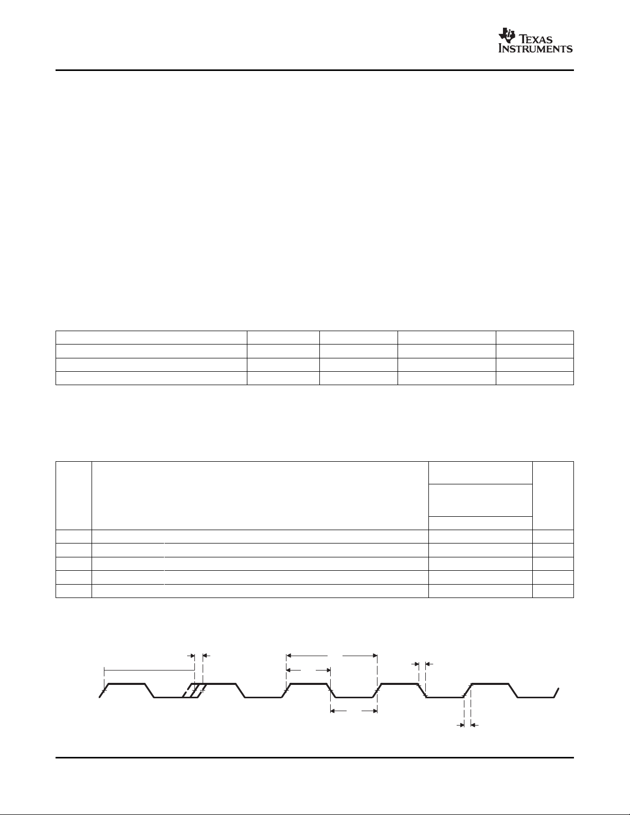
www.ti.com
PRODUCT PREVIEW
CLKIN
2
3
4
4
5
1
TMS320DM647/TMS320DM648
Digital Media Processor
SPRS372 – MAY 2007
6.4.2 PLL1 Controller Operating Modes
The PLL1 controller has two modes of operation: bypass mode and PLL mode. The mode of operation is
determined by the PLLEN bit of the PLL control register (PLLCTL). In PLL mode, SYSREFCLK is
generated from the device input clock CLKIN1 using the divider PREDIV and the PLL multiplier PLLM. In
bypass mode, CLKIN1 is fed directly to SYSREFCLK.
All hosts (HPI, PCI, etc.) must hold off accesses to the DSP while the frequency of its internal clocks is
changing. A mechanism must be in place such that the DSP notifies the host when the PLL configuration
has completed.
6.4.3 PLL1 Stabilization, Lock, and Reset Times
The PLL stabilization time is the amount of time that must be allotted for the internal PLL regulators to
become stable after device power-up. The PLL should not be operated until this stabilization time has
expired.
The PLL reset time is the amount of wait time needed when resetting the PLL (writing PLLRST = 1), in
order for the PLL to properly reset, before bringing the PLL out of reset (writing PLLRST = 0). For the
PLL1 reset time value, see Table 6-7 .
Table 6-7. PLL1 Stabilization, Lock, and Reset Times
PLL stabilization time 150 µ s
PLL lock time 2000*C
PLL reset time 128*C
(1) C = CLKIN1 cycle time in ns. For example, when CLKIN1 frequency is 50 MHz, use C = 20 ns.
6.4.4 PLL1 Controller Input and Output Clock Electrical Data/Timing
Table 6-8. Timing Requirements for CLKIN1
NO. UNIT
1 t
c(CLKIN1)
2 t
w(CLKIN1H)
3 t
w(CLKIN1L)
4 t
t(CLKIN1)
5 t
J(CLKIN1)
(1) The reference points for the rise and fall transitions are measured at 3.3-V VILMAX and VIHMIN.
(2) C = CLKIN1 cycle time in ns. For example, when CLKIN1 frequency is 50 MHz, use C = 20 ns.
(3) The PLL1 multiplier factors (x1 [BYPASS], x 15, x20, x25, x30, x32) further limit the MIN and MAX values for tc(CLKIN1). For more
detailed information on these limitations, see Section 6.3.5 , DM647/DM648 Power and Clock Domains.
Cycle time, CLKIN1 15 30.3 ns
Pulse duration, CLKIN1 high 0.4C ns
Pulse duration, CLKIN1 low 0.4C ns
Transition time, CLKIN1 1.2 ns
Period jitter, (peak-to-peak), CLKIN1 100 ps
MIN TYP MAX UNIT
(1)
(1)
(1) (2) (3)
(see Figure 6-6 )
-720
-900
PLL MODES
x1 (Bypass), x15, x20,
x25, x30, x32
MIN MAX
µ s
µ s
Peripheral Information and Electrical Specifications66 Submit Documentation Feedback
Figure 6-6. CLKIN1 Timing

www.ti.com
6.4.5 PLL1 Controller Register Description(s)
PLLV2
C162C161
EMIFilter
+1.8V
560pF 0.1 F
DM647/DM648
PLL2
CLKIN2
PLLM
x20
PLLOUTPLLREF
DDR2MemoryController
SYSCLK1(FromPLL Controller1)
A summary of the PLL1 controller registers is shown in Table 6-9 .
Table 6-9. PLL1 and Reset Controller Registers Memory Map
HEX ADDRESS RANGE REGISTER NAME DESCRIPTION
0x020E 0000 PID Peripheral Identification and Revision Information Register
0x020E 00E4 RSTYPE Reset Type Register
0x020E 0100 PLLCTL PLL Controller 1 Operations Control Register
0x020E 0110 PLLM PLL Controller 1 Multiplier Control Register
0x020E 0114 PREDIV PLL Pre-Divider Control Register
0x020E 011C PLLDIV2 PLL Controller 1 Control-Divider 2 Register (SYSCLK2)
0x020E 0138 PLLCMD PLL Controller 1 Command Register
0x020E 013C PLLSTAT PLL Controller 1 Status Register (Shows PLLC1 Status)
0x020E 0140 ALNCTL PLL Controller Clock Align Control Register
0x020E 0144 DCHANGE PLLDIV Ratio Change Status Register
0x020E 0150 SYSTAT PLL Controller 1 System Clock Status 1 Register (Indicates SYSCLK on/off
0x020E 0160 PLLDIV4 PLL Controller 1 Control-Divider 4 Register (SYSCLK4)
TMS320DM647/TMS320DM648
Digital Media Processor
SPRS372 – MAY 2007
Status)
6.5 PLL2 and PLL2 Controller
The secondary PLL controller generates interface clocks for the DDR2 memory controller.
As shown in Figure 6-7 , the PLL2 controller features a PLL multiplier controller. The PLL multiplier is fixed
to a x20 multiplier rate. PLL2 power is supplied externally via the PLL2 power supply (PLLV2). An external
PLL filter circuit must be added to PLLV2 as shown in Figure 6-7 . The 1.8-V supply for the EMI filter must
be from the same 1.8-V power plane supplying the I/O power-supply pin, DVDD18. TI requires EMI filter
manufacturer Murata, part number NFM18CC222R1C3.
Figure 6-7. PLL Controller
All PLL external components (C161, C162, and the EMI Filter) should be placed as close to the C64x+
Submit Documentation Feedback Peripheral Information and Electrical Specifications 67

www.ti.com
PRODUCT PREVIEW
CLKIN
2
3
4
4
5
1
TMS320DM647/TMS320DM648
Digital Media Processor
SPRS372 – MAY 2007
DSP device as possible. For the best performance, TI requires that all the PLL external components be on
a single side of the board without jumpers, switches, or components other than the ones shown. For
reduced PLL jitter, maximize the spacing between switching signals and the PLL external components
(C161, C162, and the EMI Filter). The minimum CLKIN2 rise and fall times should also be observed. For
the input clock timing requirements, see Section 6.5.3 , PLL2 Controller Input Clock Electrical Data/Timing.
6.5.1 PLL2 Controller Device-Specific Information
As shown in Figure 6-7 , the output of PLL2, PLLOUT, is directly fed to the DDR2 memory controller. This
clock is used by the DDR2 memory controller to generate DDR2CLKOUT and DDR2CLKOUTz. Note that,
internally, the data bus interface of the DDR2 memory controller is clocked by SYSCLK1 of the PLL1
controller.
Note that there is a minimum and maximum operating frequency for PLLREF, and PLLOUT. The clock
generator must not be configured to exceed any of these constraints. For the PLL clocks input and output
frequency ranges, see Table 6-10 .
CLOCK SIGNAL REQUIRED FREQUENCY UNIT
PLLREF (CLKIN2 ) 26.6 MHz
PLLOUT (DDR2 clock) 533 MHz
Table 6-10. PLL2 Clock Frequency Ranges
6.5.2 PLL2 Controller Operating Modes
Unlike the PLL1 controller that can operate in bypass and a PLL mode, the PLL2 controller only operates
in PLL mode. PLL2 isunlocked only during the power-up sequence (see Section 6.7 ) and is locked by the
time the RESETSTAT pin goes high. It does not lose lock during any of the other resets.
6.5.3 PLL2 Controller Input Clock Electrical Data/Timing
Table 6-11. Timing Requirements for CLKIN2
NO. UNIT
1 t
c(CLKIN2)
2 t
w(CLKIN2H)
3 t
w(CLKIN2L)
4 t
t(CLKIN2)
5 t
J(CLKIN2)
(1) The reference points for the rise and fall transitions are measured at 3.3-V VILMAX and VIHMIN.
(2) C = CLKIN2 cycle time in ns. For example, when CLKIN2 frequency is 25 MHz, use C = 40 ns.
(1) (2)
(see Figure 6-8 )
-720
-900
PLL MODES x20
MIN MAX
Cycle time, CLKIN2 37.5 37.5 ns
Pulse duration, CLKIN2 high 0.4C ns
Pulse duration, CLKIN2 low 0.4C ns
Transition time, CLKIN2 1.2 ns
Period jitter, (peak-to-peak) CLKIN2 100 ps
Figure 6-8. CLKIN2 Timing
68 Peripheral Information and Electrical Specifications Submit Documentation Feedback

www.ti.com
6.5.4 PLL1 Controller Register Description(s)
A summary of the PLL2 controller registers is shown in Table 6-12 .
Table 6-12. PLL2 and Reset Controller Registers Memory Map
HEX ADDRESS RANGE REGISTER NAME DESCRIPTION
0x0212 0000 PID Peripheral Identification and Revision Information Register
0x0212 0100 PLLCTL PLL Controller 1 Operations Control Register
0x0212 0110 PLLM PLL Controller 1 Multiplier Control Register
0x0212 0138 PLLCMD PLL Controller 1 Command Register
0x0212 013C PLLSTAT PLL Controller 1 Status Register (Shows PLLC1 Status)
TMS320DM647/TMS320DM648
Digital Media Processor
SPRS372 – MAY 2007
Submit Documentation Feedback Peripheral Information and Electrical Specifications 69

www.ti.com
PRODUCT PREVIEW
TMS320DM647/TMS320DM648
Digital Media Processor
SPRS372 – MAY 2007
6.6 Enhanced Direct Memory Access (EDMA3) Controller
The EDMA controller handles all data transfers between memories and the device slave peripherals on
the DM648 device. These data transfers include cache servicing, non-cacheable memory accesses,
user-programmed data transfers, and host accesses. These are summarized as follows:
• Transfer to/from on-chip memories
– DSP L1D memory
– DSP L2 memory
• Transfer to/from external storage
– DDR2 SDRAM
– Synchronous/Asynchronous EMIF (EMIFA)
• Transfer to/from peripherals/hosts
– VLYNQ
– HPI
– McASP
– UART
– Video Port 0/1/2/3/4
– Timer 0/1/2/3
– SPI
– I2C
6.6.1 EDMA3 Channel Synchronization Events
The EDMA supports up to 64 EDMA channels which service peripheral devices and external memory.
Table 6-13 lists the source of EDMA synchronization events associated with each of the programmable
EDMA channels. For the DM648 device, the association of an event to a channel is fixed; each of the
EDMA channels has one specific event associated with it. These specific events are captured in the
EDMA event registers (ER, ERH) even if the events are disabled by the EDMA event enable registers
(EER, EERH). For more detailed information on the EDMA module and how EDMA events are enabled,
captured, processed, linked, chained, and cleared, etc., see the TMS320DM647/DM648 DSP Enhanced
DMA (EDMA) Controller User's Guide (literature number SPRUEL2 ).
TPCC DEFAULT BINARY DEFAULT EVENT TPCC DEFAULT BINARY DEFAULT EVENT
CHANN EVENT# CHANNEL EVENT #
EL
0 0 000 0000 HPI/PCI : DSPINT 32 32 010 0000 VP2EVTYA
1 1 000 0001 TIMER0 : TINT0L 33 33 010 0001 VP2EVTUA
2 2 000 0010 TIMER0 : TINT0H 34 34 010 0010 VP2EVTVA
3 3 000 0011 TIMER2 : TINT2L 35 35 010 0011 VP2EVTYB
4 4 000 0100 TIMER2 : TINT2H 36 36 010 0100 VP2EVTUB
5 5 000 0101 TIMER3 : TINT3L 37 37 010 0101 VP2EVTVB
6 6 000 0110 TIMER3 : TINT3H 38 38 010 0110 VP3EVTYA
7 7 000 0111 IMCOP: IMXINT 39 39 010 0111 VP3EVTUA
8 8 000 1000 IMCOP: VLCDINT 40 40 010 1000 VP3EVTVA
9 9 000 1001 IMCOP: DSQINT 41 41 010 1001 VP3EVTYB
10 10 000 1010 McASP: AXEVTE 42 42 010 1010 VP3EVTUB
11 11 000 1011 McASP: AXEVTO 43 43 010 1011 VP3EVTVB
12 12 000 1100 McASP: AXEVT 44 44 010 1100 ICREVT
13 13 000 1101 McASP: AREVTE 45 45 010 1101 ICXEVT
14 14 000 1110 McASP: AREVTO 46 46 010 1110 SPI: SPIXEVT
Table 6-13. EDMA Channel Synchronization Events
Peripheral Information and Electrical Specifications70 Submit Documentation Feedback

www.ti.com
TMS320DM647/TMS320DM648
Digital Media Processor
Table 6-13. EDMA Channel Synchronization Events (continued)
TPCC DEFAULT BINARY DEFAULT EVENT TPCC DEFAULT BINARY DEFAULT EVENT
CHANN EVENT# CHANNEL EVENT #
EL
15 15 000 1111 McASP: AREVT 47 47 010 1111 SPI: SPIREVT
16 16 001 0000 TIMER1 : TINT1L 48 48 011 0000 VP4EVTYA
17 17 001 0001 TIMER1 : TINT1H 49 49 011 0001 VP4EVTUA
18 18 001 0010 UART: URXEVT 50 50 011 0010 VP4EVTVA
19 19 001 0011 UART: UTXEVT 51 51 011 0011 VP4EVTYB
20 20 001 0100 VP0EVTYA 52 52 011 0100 VP4EVTUB
21 21 001 0101 VP0EVTUA 53 53 011 0101 VP4EVTVB
22 22 001 0110 VP0EVTVA 54 54 011 0110 GPIO : GPINT6
23 23 001 0111 VP0EVTYB 55 55 011 0111 GPIO : GPINT7
24 24 001 1000 VP0EVTUB 56 56 011 1000 GPIO : GPINT8
25 25 001 1001 VP0EVTVB 57 57 011 1001 GPIO : GPINT9
26 26 001 1010 VP1EVTYA 58 58 011 1010 GPIO : GPINT10
27 27 001 1011 VP1EVTUA 59 59 011 1011 GPIO : GPINT11
28 28 001 1100 VP1EVTVA 60 60 011 1100 GPIO : GPINT12
29 29 001 1101 VP1EVTYB 61 61 011 1101 GPIO : GPINT13
30 30 001 1110 VP1EVTUB 62 62 011 1110 GPIO : GPINT14
31 31 001 1111 VP1EVTVB 63 63 011 1111 GPIO : GPINT15
SPRS372 – MAY 2007
6.6.2 EDMA Peripheral Register Description(s)
Table 6-14 lists the EDMA registers, their corresponding acronyms, and DM648 device memory locations.
Table 6-14. DM647/DM648 EDMA Channel Controller Registers
HEX ADDRESS ACRONYM REGISTER NAME
0x02A0 0000 PID Peripheral ID Register
0x02A0 0004 CCCFG EDMA3CC Configuration Register
0x02A0 0008 - 0x02A0 00FC Reserved
0x02A0 0100 DCHMAP0 DMA Channel 0 Mapping Register
0x02A0 0104 DCHMAP1 DMA Channel 1 Mapping Register
0x02A0 0108 DCHMAP2 DMA Channel 2 Mapping Register
0x02A0 010C DCHMAP3 DMA Channel 3 Mapping Register
0x02A0 0110 DCHMAP4 DMA Channel 4 Mapping Register
0x02A0 0114 DCHMAP5 DMA Channel 5 Mapping Register
0x02A0 0118 DCHMAP6 DMA Channel 6 Mapping Register
0x02A0 011C DCHMAP7 DMA Channel 7 Mapping Register
0x02A0 0120 DCHMAP8 DMA Channel 8 Mapping Register
0x02A0 0124 DCHMAP9 DMA Channel 9 Mapping Register
0x02A0 0128 DCHMAP10 DMA Channel 10 Mapping Register
0x02A0 012C DCHMAP11 DMA Channel 11 Mapping Register
0x02A0 0130 DCHMAP12 DMA Channel 12 Mapping Register
0x02A0 0134 DCHMAP13 DMA Channel 13 Mapping Register
0x02A0 0138 DCHMAP14 DMA Channel 14 Mapping Register
0x02A0 013C DCHMAP15 DMA Channel 15 Mapping Register
0x02A0 0140 DCHMAP16 DMA Channel 16 Mapping Register
0x02A0 0144 DCHMAP17 DMA Channel 17 Mapping Register
0x02A0 0148 DCHMAP18 DMA Channel 18 Mapping Register
Submit Documentation Feedback Peripheral Information and Electrical Specifications 71

www.ti.com
PRODUCT PREVIEW
TMS320DM647/TMS320DM648
Digital Media Processor
SPRS372 – MAY 2007
Table 6-14. DM647/DM648 EDMA Channel Controller Registers (continued)
HEX ADDRESS ACRONYM REGISTER NAME
0x02A0 014C DCHMAP19 DMA Channel 19 Mapping Register
0x02A0 0150 DCHMAP20 DMA Channel 20 Mapping Register
0x02A0 0154 DCHMAP21 DMA Channel 21 Mapping Register
0x02A0 0158 DCHMAP22 DMA Channel 22 Mapping Register
0x02A0 015C DCHMAP23 DMA Channel 23 Mapping Register
0x02A0 0160 DCHMAP24 DMA Channel 24 Mapping Register
0x02A0 0164 DCHMAP25 DMA Channel 25 Mapping Register
0x02A0 0168 DCHMAP26 DMA Channel 26 Mapping Register
0x02A0 016C DCHMAP27 DMA Channel 27 Mapping Register
0x02A0 0170 DCHMAP28 DMA Channel 28 Mapping Register
0x02A0 0174 DCHMAP29 DMA Channel 29 Mapping Register
0x02A0 0178 DCHMAP30 DMA Channel 30 Mapping Register
0x02A0 017C DCHMAP31 DMA Channel 31 Mapping Register
0x02A0 0180 DCHMAP32 DMA Channel 32 Mapping Register
0x02A0 0184 DCHMAP33 DMA Channel 33 Mapping Register
0x02A0 0188 DCHMAP34 DMA Channel 34 Mapping Register
0x02A0 018C DCHMAP35 DMA Channel 35 Mapping Register
0x02A0 0190 DCHMAP36 DMA Channel 36 Mapping Register
0x02A0 0194 DCHMAP37 DMA Channel 37 Mapping Register
0x02A0 0198 DCHMAP38 DMA Channel 38 Mapping Register
0x02A0 019C DCHMAP39 DMA Channel 39 Mapping Register
0x02A0 01A0 DCHMAP40 DMA Channel 40 Mapping Register
0x02A0 01A4 DCHMAP41 DMA Channel 41 Mapping Register
0x02A0 01A8 DCHMAP42 DMA Channel 42 Mapping Register
0x02A0 01AC DCHMAP43 DMA Channel 43 Mapping Register
0x02A0 01B0 DCHMAP44 DMA Channel 44 Mapping Register
0x02A0 01B4 DCHMAP45 DMA Channel 45 Mapping Register
0x02A0 01B8 DCHMAP46 DMA Channel 46 Mapping Register
0x02A0 01BC DCHMAP47 DMA Channel 47 Mapping Register
0x02A0 01C0 DCHMAP48 DMA Channel 48 Mapping Register
0x02A0 01C4 DCHMAP49 DMA Channel 49 Mapping Register
0x02A0 01C8 DCHMAP50 DMA Channel 50 Mapping Register
0x02A0 01CC DCHMAP51 DMA Channel 51 Mapping Register
0x02A0 01D0 DCHMAP52 DMA Channel 52 Mapping Register
0x02A0 01D4 DCHMAP53 DMA Channel 53 Mapping Register
0x02A0 01D8 DCHMAP54 DMA Channel 54 Mapping Register
0x02A0 01DC DCHMAP55 DMA Channel 55 Mapping Register
0x02A0 01E0 DCHMAP56 DMA Channel 56 Mapping Register
0x02A0 01E4 DCHMAP57 DMA Channel 57 Mapping Register
0x02A0 01E8 DCHMAP58 DMA Channel 58 Mapping Register
0x02A0 01EC DCHMAP59 DMA Channel 59 Mapping Register
0x02A0 01F0 DCHMAP60 DMA Channel 60 Mapping Register
0x02A0 01F4 DCHMAP61 DMA Channel 61 Mapping Register
0x02A0 01F8 DCHMAP62 DMA Channel 62 Mapping Register
0x02A0 01FC DCHMAP63 DMA Channel 63 Mapping Register
0x02A0 0200 QCHMAP0 QDMA Channel 0 Mapping to PaRAM Register
0x02A0 0204 QCHMAP1 QDMA Channel 1 Mapping to PaRAM Register
Peripheral Information and Electrical Specifications72 Submit Documentation Feedback

www.ti.com
TMS320DM647/TMS320DM648
Table 6-14. DM647/DM648 EDMA Channel Controller Registers (continued)
HEX ADDRESS ACRONYM REGISTER NAME
0x02A0 0208 QCHMAP2 QDMA Channel 2 Mapping to PaRAM Register
0x02A0 020C QCHMAP3 QDMA Channel 3 Mapping to PaRAM Register
0x02A0 0210 QCHMAP4 QDMA Channel 4 Mapping to PaRAM Register
0x02A0 0214 QCHMAP5 QDMA Channel 5 Mapping to PaRAM Register
0x02A0 0218 QCHMAP6 QDMA Channel 6 Mapping to PaRAM Register
0x02A0 021C QCHMAP7 QDMA Channel 7 Mapping to PaRAM Register
0x02A0 0220 - 0x02A0 021C - Reserved
0x02A0 0220 - 0x02A0 023C - Reserved
0x02A0 0240 DMAQNUM0 DMA Queue Number Register 0 (Channels 00 to 07)
0x02A0 0244 DMAQNUM1 DMA Queue Number Register 1 (Channels 08 to 15)
0x02A0 0248 DMAQNUM2 DMA Queue Number Register 2 (Channels 16 to 23)
0x02A0 024C DMAQNUM3 DMA Queue Number Register 3 (Channels 24 to 31)
0x02A0 0250 - 0x02A0 025C - Reserved
0x02A0 0260 QDMAQNUM CC QDMA Queue Number
0x02A0 0264 - 0x02A0 0280 – Reserved
0x02A0 0284 QUEPRI Queue Priority Register
0x02A0 0288 - 0x02A0 02FC – Reserved
0x02A0 0300 EMR Event Missed Register
0x02A0 0304 EMRH Event Missed Register High
0x02A0 0308 EMCR Event Missed Clear Register
0x02A0 030C EMCRH Event Missed Clear Register High
0x02A0 0310 QEMR QDMA Event Missed Register
0x02A0 0314 QEMCR QDMA Event Missed Clear Register
0x02A0 0318 CCERR EDMA3CC Error Register
0x02A0 031C CCERRCLR EDMA3CC Error Clear Register
0x02A0 0320 EEVAL Error Evaluate Register
0x02A0 0324 - 0x02A0 033C - Reserved
0x02A0 0340 DRAE0 DMA Region Access Enable Register for Region 0
0x02A0 0344 DRAEH0 DMA Region Access Enable Register High for Region 0
0x02A0 0348 DRAE1 DMA Region Access Enable Register for Region 1
0x02A0 034C DRAEH1 DMA Region Access Enable Register High for Region 1
0x02A0 0350 DRAE2 DMA Region Access Enable Register for Region 2
0x02A0 0354 DRAEH2 DMA Region Access Enable Register High for Region 2
0x02A0 0358 DRAE3 DMA Region Access Enable Register for Region 3
0x02A0 035C DRAEH3 DMA Region Access Enable Register High for Region 3
0x02A0 0360 DRAE4 DMA Region Access Enable Register for Region 4
0x02A0 0364 DRAEH4 DMA Region Access Enable Register High for Region 4
0x02A0 0368 DRAE5 DMA Region Access Enable Register for Region 5
0x02A0 036C DRAEH5 DMA Region Access Enable Register High for Region 5
0x02A0 0370 DRAE6 DMA Region Access Enable Register for Region 6
0x02A0 0374 DRAEH6 DMA Region Access Enable Register High for Region 6
0x02A0 0378 DRAE7 DMA Region Access Enable Register for Region 7
0x02A0 037C DRAEH7 DMA Region Access Enable Register High for Region 7
0x02A0 0380 QRAE0 QDMA Region Access Enable Register for Region 0
0x02A0 0384 QRAE1 QDMA Region Access Enable Register for Region 1
0x02A0 0388 QRAE2 QDMA Region Access Enable Register for Region 2
0x02A0 038C QRAE3 QDMA Region Access Enable Register for Region 3
Digital Media Processor
SPRS372 – MAY 2007
Submit Documentation Feedback Peripheral Information and Electrical Specifications 73

www.ti.com
PRODUCT PREVIEW
TMS320DM647/TMS320DM648
Digital Media Processor
SPRS372 – MAY 2007
Table 6-14. DM647/DM648 EDMA Channel Controller Registers (continued)
HEX ADDRESS ACRONYM REGISTER NAME
0x02A0 0390 - 0x02A0 039C – Reserved
0x02A0 0400 Q0E0 Event Queue 0 Entry Register 0
0x02A0 0404 Q0E1 Event Queue 0 Entry Register 1
0x02A0 0408 Q0E2 Event Queue 0 Entry Register 2
0x02A0 040C Q0E3 Event Queue 0 Entry Register 3
0x02A0 0410 Q0E4 Event Queue 0 Entry Register 4
0x02A0 0414 Q0E5 Event Queue 0 Entry Register 5
0x02A0 0418 Q0E6 Event Queue 0 Entry Register 6
0x02A0 041C Q0E7 Event Queue 0 Entry Register 7
0x02A0 0420 Q0E8 Event Queue 0 Entry Register 8
0x02A0 0424 Q0E9 Event Queue 0 Entry Register 9
0x02A0 0428 Q0E10 Event Queue 0 Entry Register 10
0x02A0 042C Q0E11 Event Queue 0 Entry Register 11
0x02A0 0430 Q0E12 Event Queue 0 Entry Register 12
0x02A0 0434 Q0E13 Event Queue 0 Entry Register 13
0x02A0 0438 Q0E14 Event Queue 0 Entry Register 14
0x02A0 043C Q0E15 Event Queue 0 Entry Register 15
0x02A0 0440 Q1E0 Event Queue 1 Entry Register 0
0x02A0 0444 Q1E1 Event Queue 1 Entry Register 1
0x02A0 0448 Q1E2 Event Queue 1 Entry Register 2
0x02A0 044C Q1E3 Event Queue 1 Entry Register 3
0x02A0 0450 Q1E4 Event Queue 1 Entry Register 4
0x02A0 0454 Q1E5 Event Queue 1 Entry Register 5
0x02A0 0458 Q1E6 Event Queue 1 Entry Register 6
0x02A0 045C Q1E7 Event Queue 1 Entry Register 7
0x02A0 0460 Q1E8 Event Queue 1 Entry Register 8
0x02A0 0464 Q1E9 Event Queue 1 Entry Register 9
0x02A0 0468 Q1E10 Event Queue 1 Entry Register 10
0x02A0 046C Q1E11 Event Queue 1 Entry Register 11
0x02A0 0470 Q1E12 Event Queue 1 Entry Register 12
0x02A0 0474 Q1E13 Event Queue 1 Entry Register 13
0x02A0 0478 Q1E14 Event Queue 1 Entry Register 14
0x02A0 047C Q1E15 Event Queue 1 Entry Register 15
0x02A0 0480 Q2E0 Event Queue 2 Entry Register 0
0x02A0 0484 Q2E1 Event Queue 2 Entry Register 1
0x02A0 0488 Q2E2 Event Queue 2 Entry Register 2
0x02A0 048C Q2E3 Event Queue 2 Entry Register 3
0x02A0 0490 Q2E4 Event Queue 2 Entry Register 4
0x02A0 0494 Q2E5 Event Queue 2 Entry Register 5
0x02A0 0498 Q2E6 Event Queue 2 Entry Register 6
0x02A0 049C Q2E7 Event Queue 2 Entry Register 7
0x02A0 04A0 Q2E8 Event Queue 2 Entry Register 8
0x02A0 04A4 Q2E9 Event Queue 2 Entry Register 9
0x02A0 04A8 Q2E10 Event Queue 2 Entry Register 10
0x02A0 04AC Q2E11 Event Queue 2 Entry Register 11
0x02A0 04B0 Q2E12 Event Queue 2 Entry Register 12
0x02A0 04B4 Q2E13 Event Queue 2 Entry Register 13
Peripheral Information and Electrical Specifications74 Submit Documentation Feedback

www.ti.com
Table 6-14. DM647/DM648 EDMA Channel Controller Registers (continued)
HEX ADDRESS ACRONYM REGISTER NAME
0x02A0 04B8 Q2E14 Event Queue 2 Entry Register 14
0x02A0 04BC Q2E15 Event Queue 2 Entry Register 15
0x02A0 04C0 Q3E0 Event Queue 3 Entry Register 0
0x02A0 04C4 Q3E1 Event Queue 3 Entry Register 1
0x02A0 04C8 Q3E2 Event Queue 3 Entry Register 2
0x02A0 04CC Q3E3 Event Queue 3 Entry Register 3
0x02A0 04D0 Q3E4 Event Queue 3 Entry Register 4
0x02A0 04D4 Q3E5 Event Queue 3 Entry Register 5
0x02A0 04D8 Q3E6 Event Queue 3 Entry Register 6
0x02A0 04DC Q3E7 Event Queue 3 Entry Register 7
0x02A0 04E0 Q3E8 Event Queue 3 Entry Register 8
0x02A0 04E4 Q3E9 Event Queue 3 Entry Register 9
0x02A0 04E8 Q3E10 Event Queue 3 Entry Register 10
0x02A0 04EC Q3E11 Event Queue 3 Entry Register 11
0x02A0 04F0 Q3E12 Event Queue 3 Entry Register 12
0x02A0 04F4 Q3E13 Event Queue 3 Entry Register 13
0x02A0 04F8 Q3E14 Event Queue 3 Entry Register 14
0x02A0 04FC Q3E15 Event Queue 3 Entry Register 15
0x02A0 0500 - 0x02A0 051C - Reserved
0x02A0 0520 - 0x02A0 05FC - Reserved
0x02A0 0600 QSTAT0 Queue 0 Status Register
0x02A0 0604 QSTAT1 Queue 1 Status Register
0x02A0 0608 QSTAT2 Queue Status Register 2
0x02A0 060C QSTAT3 Queue Status Register 3
0x02A0 0610 - 0x02A0 061C - Reserved
0x02A0 0620 QWMTHRA Queue Watermark Threshold A Register for Q[3:0]
0x02A0 0624 – Reserved
0x02A0 0640 CCSTAT EDMA3CC Status Register
0x02A0 0644 - 0x02A0 06FC - Reserved
0x02A0 0700 - 0x02A0 0FFC - Reserved
0x02A0 1000 ER Event Register
0x02A0 1004 ERH Event Register High
0x02A0 1008 ECR Event Clear Register
0x02A0 100C ECRH Event Clear Register High
0x02A0 1010 ESR Event Set Register
0x02A0 1014 ESRH Event Set Register High
0x02A0 1018 CER Chained Event Register
0x02A0 101C CERH Chained Event Register High
0x02A0 1020 EER Event Enable Register
0x02A0 1024 EERH Event Enable Register High
0x02A0 1028 EECR Event Enable Clear Register
0x02A0 102C EECRH Event Enable Clear Register High
0x02A0 1030 EESR Event Enable Set Register
0x02A0 1034 EESRH Event Enable Set Register High
0x02A0 1038 SER Secondary Event Register
0x02A0 103C SERH Secondary Event Register High
0x02A0 1040 SECR Secondary Event Clear Register
TMS320DM647/TMS320DM648
Digital Media Processor
SPRS372 – MAY 2007
Submit Documentation Feedback Peripheral Information and Electrical Specifications 75

www.ti.com
PRODUCT PREVIEW
TMS320DM647/TMS320DM648
Digital Media Processor
SPRS372 – MAY 2007
Table 6-14. DM647/DM648 EDMA Channel Controller Registers (continued)
HEX ADDRESS ACRONYM REGISTER NAME
0x02A0 1044 SECRH Secondary Event Clear Register High
0x02A0 1048 - 0x02A0 104C Reserved
0x02A0 1050 IER Interrupt Enable Register
0x02A0 1054 IERH Interrupt Enable Register High
0x02A0 1058 IECR Interrupt Enable Clear Register
0x02A0 105C IECRH Interrupt Enable Clear Register High
0x02A0 1060 IESR Interrupt Enable Set Register
0x02A0 1064 IESRH Interrupt Enable Set Register High
0x02A0 1068 IPR Interrupt Pending Register
0x02A0 106C IPRH Interrupt Pending Register High
0x02A0 1070 ICR Interrupt Clear Register
0x02A0 1074 ICRH Interrupt Clear Register High
0x02A0 1078 IEVAL Interrupt Evaluate Register
0x02A0 107C - Reserved
0x02A0 1080 QER QDMA Event Register
0x02A0 1084 QEER QDMA Event Enable Register
0x02A0 1088 QEECR QDMA Event Enable Clear Register
0x02A0 108C QEESR QDMA Event Enable Set Register
0x02A0 1090 QSER QDMA Secondary Event Register
0x02A0 1094 QSECR QDMA Secondary Event Clear Register
0x02A0 1098 - 0x02A0 1FFF - Reserved
0x02A0 2000- 0x02A0 2097 - Shadow Region 0 Channel Registers
0x02A0 2098 - 0x02A0 21FF - Reserved
0x02A0 2200 - 0x02A0 2297 - Shadow Region 1 Channel Registers
0x02A0 2298 - 0x02A0 23FF - Reserved
0x02A0 2400 - 0x02A0 2497 - Shadow Region 2 Channel Registers
0x02A0 2498 - 0x02A0 25FF - Reserved
0x02A0 2600 - 0x02A0 2697 - Shadow Region 3 Channel Registers
0x02A0 2698 - 0x02A0 27FF - Reserved
0x02A0 2800 - 0x02A0 2897 - Shadow Region 4 Channel Registers
0x02A0 2898 - 0x02A0 29FF - Reserved
0x02A0 2A00 - 0x02A0 2A97 - Shadow Region 5 Channel Registers
0x02A0 2A98 - 0x02A0 2BFF - Reserved
0x02A0 2C00 - 0x02A0 2C97 - Shadow Region 6 Channel Registers
0x02A0 2C98 - 0x02A0 2DFF - Reserved
0x02A0 2E00 - 0x02A0 2E97 - Shadow Region 7 Channel Registers
0x02A0 2E98 - 0x02A0 2FFF - Reserved
Table 6-15 shows an abbreviation of the set of registers which make up the parameter set for each of 128
EDMA events. Each of the parameter register sets consist of eight 32-bit word entries. Table 6-16 shows
the parameter set entry registers with relative memory address locations within each of the parameter
sets.
Peripheral Information and Electrical Specifications76 Submit Documentation Feedback

www.ti.com
Table 6-15. EDMA Parameter Set RAM
HEX ADDRESS RANGE DESCRIPTION
0x02A0 4000 - 0x02A0 401F Parameters Set 0 (8 32-bit words)
0x02A0 4020 - 0x02A0 403F Parameters Set 1 (8 32-bit words)
0x02A0 4040 - 0x02A0 405F Parameters Set 2 (8 32-bit words)
0x02A0 4060 - 0x02A0 407F Parameters Set 3 (8 32-bit words)
0x02A0 4080 - 0x02A0 409F Parameters Set 4 (8 32-bit words)
0x02A0 40A0 - 0x02A0 40BF Parameters Set 5 (8 32-bit words)
... ...
0x02A0 4FC0 - 0x02A0 4FDF Parameters Set 126 (8 32-bit words)
0x02A0 4FE0 - 0x02A0 4FFF Parameters Set 127 (8 32-bit words)
... ...
0x02A0 5FC0 - 0x02A0 5FDF Parameters Set 254 (8 32-bit words)
0x02A0 5FE0 - 0x02A0 5FFF Parameters Set 255 (8 32-bit words)
... ...
0x02A0 7FC0 - 0x02A0 7FDF Parameters Set 510 (8 32-bit words)
0x02A0 7FE0 - 0x02A0 7FFF Parameters Set 511 (8 32-bit words)
TMS320DM647/TMS320DM648
Digital Media Processor
SPRS372 – MAY 2007
Table 6-16. Parameter Set Entries
HEX OFFSET ADDRESS
WITHIN THE PARAMETER SET
0x0000 OPT Option
0x0004 SRC Source Address
0x0008 A_B_CNT A Count, B Count
0x000C DST Destination Address
0x0010 SRC_DST_BIDX Source B Index, Destination B Index
0x0014 LINK_BCNTRLD Link Address, B Count Reload
0x0018 SRC_DST_CIDX Source C Index, Destination C Index
0x001C CCNT C Count
Table 6-17. EDMA3 Transfer Controller 0 Registers
HEX ADDRESS RANGE ACRONYM REGISTER NAME
02A2 0000 PID Peripheral Identification Register
02A2 0004 TCCFG EDMA3TC Configuration Register
02A2 0008 - 02A2 00FC - Reserved
02A2 0100 TCSTAT EDMA3TC Channel Status Register
02A2 0104 - 02A2 011C - Reserved
02A2 0120 ERRSTAT Error Register
02A2 0124 ERREN Error Enable Register
02A2 0128 ERRCLR Error Clear Register
02A2 012C ERRDET Error Details Register
02A2 0130 ERRCMD Error Interrupt Command Register
02A2 0134 - 02A2 013C - Reserved
02A2 0140 RDRATE Read Rate Register
02A2 0144 - 02A2 023C - Reserved
02A2 0240 SAOPT Source Active Options Register
02A2 0244 SASRC Source Active Source Address Register
ACRONYM PARAMETER ENTRY
Submit Documentation Feedback Peripheral Information and Electrical Specifications 77

www.ti.com
PRODUCT PREVIEW
TMS320DM647/TMS320DM648
Digital Media Processor
SPRS372 – MAY 2007
Table 6-17. EDMA3 Transfer Controller 0 Registers (continued)
HEX ADDRESS RANGE ACRONYM REGISTER NAME
02A2 0248 SACNT Source Active Count Register
02A2 024C SADST Source Active Destination Address Register
02A2 0250 SABIDX Source Active Source B-Index Register
02A2 0254 SAMPPRXY Source Active Memory Protection Proxy Register
02A2 0258 SACNTRLD Source Active Count Reload Register
02A2 025C SASRCBREF Source Active Source Address B-Reference Register
02A2 0260 SADSTBREF Source Active Destination Address B-Reference Register
02A2 0264 - 02A2 027C - Reserved
02A2 0280 DFCNTRLD Destination FIFO Set Count Reload
02A2 0284 DFSRCBREF Destination FIFO Set Destination Address B Reference Register
02A2 0288 DFDSTBREF Destination FIFO Set Destination Address B Reference Register
02A2 028C - 02A2 02FC - Reserved
02A2 0300 DFOPT0 Destination FIFO Options Register 0
02A2 0304 DFSRC0 Destination FIFO Source Address Register 0
02A2 0308 DFCNT0 Destination FIFO Count Register 0
02A2 030C DFDST0 Destination FIFO Destination Address Register 0
02A2 0310 DFBIDX0 Destination FIFO BIDX Register 0
02A2 0314 DFMPPRXY0 Destination FIFO Memory Protection Proxy Register 0
02A2 0318 - 02A2 033C - Reserved
02A2 0340 DFOPT1 Destination FIFO Options Register 1
02A2 0344 DFSRC1 Destination FIFO Source Address Register 1
02A2 0348 DFCNT1 Destination FIFO Count Register 1
02A2 034C DFDST1 Destination FIFO Destination Address Register 1
02A2 0350 DFBIDX1 Destination FIFO BIDX Register 1
02A2 0354 DFMPPRXY1 Destination FIFO Memory Protection Proxy Register 1
02A2 0358 - 02A2 037C - Reserved
02A2 0380 DFOPT2 Destination FIFO Options Register 2
02A2 0384 DFSRC2 Destination FIFO Source Address Register 2
02A2 0388 DFCNT2 Destination FIFO Count Register 2
02A2 038C DFDST2 Destination FIFO Destination Address Register 2
02A2 0390 DFBIDX2 Destination FIFO BIDX Register 2
02A2 0394 DFMPPRXY2 Destination FIFO Memory Protection Proxy Register 2
02A2 0398 - 02A2 03BC - Reserved
02A2 03C0 DFOPT3 Destination FIFO Options Register 3
02A2 03C4 DFSRC3 Destination FIFO Source Address Register 3
02A2 03C8 DFCNT3 Destination FIFO Count Register 3
02A2 03CC DFDST3 Destination FIFO Destination Address Register 3
02A2 03D0 DFBIDX3 Destination FIFO BIDX Register 3
02A2 03D4 DFMPPRXY3 Destination FIFO Memory Protection Proxy Register 3
02A2 03D8 - 02A2 7FFF - Reserved
Table 6-18. EDMA3 Transfer Controller 1 Registers
HEX ADDRESS RANGE ACRONYM REGISTER NAME
02A2 8000 PID Peripheral Identification Register
02A2 8004 TCCFG EDMA3TC Configuration Register
02A2 8008 - 02A2 80FC - Reserved
Peripheral Information and Electrical Specifications78 Submit Documentation Feedback

www.ti.com
Table 6-18. EDMA3 Transfer Controller 1 Registers (continued)
HEX ADDRESS RANGE ACRONYM REGISTER NAME
02A2 8100 TCSTAT EDMA3TC Channel Status Register
02A2 8104 - 02A2 811C - Reserved
02A2 8120 ERRSTAT Error Register
02A2 8124 ERREN Error Enable Register
02A2 8128 ERRCLR Error Clear Register
02A2 812C ERRDET Error Details Register
02A2 8130 ERRCMD Error Interrupt Command Register
02A2 8134 - 02A2 813C - Reserved
02A2 8140 RDRATE Read Rate Register
02A2 8144 - 02A2 823C - Reserved
02A2 8240 SAOPT Source Active Options Register
02A2 8244 SASRC Source Active Source Address Register
02A2 8248 SACNT Source Active Count Register
02A2 824C SADST Source Active Destination Address Register
02A2 8250 SABIDX Source Active Source B-Index Register
02A2 8254 SAMPPRXY Source Active Memory Protection Proxy Register
02A2 8258 SACNTRLD Source Active Count Reload Register
02A2 825C SASRCBREF Source Active Source Address B-Reference Register
02A2 8260 SADSTBREF Source Active Destination Address B-Reference Register
02A2 8264 - 02A2 827C - Reserved
02A2 8280 DFCNTRLD Destination FIFO Set Count Reload
02A2 8284 DFSRCBREF Destination FIFO Set Destination Address B Reference Register
02A2 8288 DFDSTBREF Destination FIFO Set Destination Address B Reference Register
02A2 828C - 02A2 82FC - Reserved
02A2 8300 DFOPT0 Destination FIFO Options Register 0
02A2 8304 DFSRC0 Destination FIFO Source Address Register 0
02A2 8308 DFCNT0 Destination FIFO Count Register 0
02A2 830C DFDST0 Destination FIFO Destination Address Register 0
02A2 8310 DFBIDX0 Destination FIFO BIDX Register 0
02A2 8314 DFMPPRXY0 Destination FIFO Memory Protection Proxy Register 0
02A2 8318 - 02A2 833C - Reserved
02A2 8340 DFOPT1 Destination FIFO Options Register 1
02A2 8344 DFSRC1 Destination FIFO Source Address Register 1
02A2 8348 DFCNT1 Destination FIFO Count Register 1
02A2 834C DFDST1 Destination FIFO Destination Address Register 1
02A2 8350 DFBIDX1 Destination FIFO BIDX Register 1
02A2 8354 DFMPPRXY1 Destination FIFO Memory Protection Proxy Register 1
02A2 8358 - 02A2 837C - Reserved
02A2 8380 DFOPT2 Destination FIFO Options Register 2
02A2 8384 DFSRC2 Destination FIFO Source Address Register 2
02A2 8388 DFCNT2 Destination FIFO Count Register 2
02A2 838C DFDST2 Destination FIFO Destination Address Register 2
02A2 8390 DFBIDX2 Destination FIFO BIDX Register 2
02A2 8394 DFMPPRXY2 Destination FIFO Memory Protection Proxy Register 2
02A2 8398 - 02A2 83BC - Reserved
02A2 83C0 DFOPT3 Destination FIFO Options Register 3
02A2 83C4 DFSRC3 Destination FIFO Source Address Register 3
TMS320DM647/TMS320DM648
Digital Media Processor
SPRS372 – MAY 2007
Submit Documentation Feedback Peripheral Information and Electrical Specifications 79

www.ti.com
PRODUCT PREVIEW
TMS320DM647/TMS320DM648
Digital Media Processor
SPRS372 – MAY 2007
Table 6-18. EDMA3 Transfer Controller 1 Registers (continued)
HEX ADDRESS RANGE ACRONYM REGISTER NAME
02A2 83C8 DFCNT3 Destination FIFO Count Register 3
02A2 83CC DFDST3 Destination FIFO Destination Address Register 3
02A2 83D0 DFBIDX3 Destination FIFO BIDX Register 3
02A2 83D4 DFMPPRXY3 Destination FIFO Memory Protection Proxy Register 3
02A2 83D8 - 02A2 FFFF - Reserved
HEX ADDRESS RANGE ACRONYM REGISTER NAME
02A3 0000 PID Peripheral Identification Register
02A3 0004 TCCFG EDMA3TC Configuration Register
02A3 0008 - 02A3 00FC - Reserved
02A3 0100 TCSTAT EDMA3TC Channel Status Register
02A3 0104 - 02A3 011C - Reserved
02A3 0120 ERRSTAT Error Register
02A3 0124 ERREN Error Enable Register
02A3 0128 ERRCLR Error Clear Register
02A3 012C ERRDET Error Details Register
02A3 0130 ERRCMD Error Interrupt Command Register
02A3 0134 - 02A3 013C - Reserved
02A3 0140 RDRATE Read Rate Register
02A3 0144 - 02A3 023C - Reserved
02A3 0240 SAOPT Source Active Options Register
02A3 0244 SASRC Source Active Source Address Register
02A3 0248 SACNT Source Active Count Register
02A3 024C SADST Source Active Destination Address Register
02A3 0250 SABIDX Source Active Source B-Index Register
02A3 0254 SAMPPRXY Source Active Memory Protection Proxy Register
02A3 0258 SACNTRLD Source Active Count Reload Register
02A3 025C SASRCBREF Source Active Source Address B-Reference Register
02A3 0260 SADSTBREF Source Active Destination Address B-Reference Register
02A3 0264 - 02A3 027C - Reserved
02A3 0280 DFCNTRLD Destination FIFO Set Count Reload
02A3 0284 DFSRCBREF Destination FIFO Set Destination Address B Reference Register
02A3 0288 DFDSTBREF Destination FIFO Set Destination Address B Reference Register
02A3 028C - 02A3 02FC - Reserved
02A3 0300 DFOPT0 Destination FIFO Options Register 0
02A3 0304 DFSRC0 Destination FIFO Source Address Register 0
02A3 0308 DFCNT0 Destination FIFO Count Register 0
02A3 030C DFDST0 Destination FIFO Destination Address Register 0
02A3 0310 DFBIDX0 Destination FIFO BIDX Register 0
02A3 0314 DFMPPRXY0 Destination FIFO Memory Protection Proxy Register 0
02A3 0318 - 02A3 033C - Reserved
02A3 0340 DFOPT1 Destination FIFO Options Register 1
02A3 0344 DFSRC1 Destination FIFO Source Address Register 1
02A3 0348 DFCNT1 Destination FIFO Count Register 1
02A3 034C DFDST1 Destination FIFO Destination Address Register 1
Table 6-19. EDMA3 Transfer Controller 2 Registers
Peripheral Information and Electrical Specifications80 Submit Documentation Feedback

www.ti.com
Table 6-19. EDMA3 Transfer Controller 2 Registers (continued)
HEX ADDRESS RANGE ACRONYM REGISTER NAME
02A3 0350 DFBIDX1 Destination FIFO BIDX Register 1
02A3 0354 DFMPPRXY1 Destination FIFO Memory Protection Proxy Register 1
02A3 0358 - 02A3 037C - Reserved
02A3 0380 DFOPT2 Destination FIFO Options Register 2
02A3 0384 DFSRC2 Destination FIFO Source Address Register 2
02A3 0388 DFCNT2 Destination FIFO Count Register 2
02A3 038C DFDST2 Destination FIFO Destination Address Register 2
02A3 0390 DFBIDX2 Destination FIFO BIDX Register 2
02A3 0394 DFMPPRXY2 Destination FIFO Memory Protection Proxy Register 2
02A3 0398 - 02A3 03BC - Reserved
02A3 03C0 DFOPT3 Destination FIFO Options Register 3
02A3 03C4 DFSRC3 Destination FIFO Source Address Register 3
02A3 03C8 DFCNT3 Destination FIFO Count Register 3
02A3 03CC DFDST3 Destination FIFO Destination Address Register 3
02A3 03D0 DFBIDX3 Destination FIFO BIDX Register 3
02A3 03D4 DFMPPRXY3 Destination FIFO Memory Protection Proxy Register 3
02A3 03D8 - 02A3 7FFF - Reserved
TMS320DM647/TMS320DM648
Digital Media Processor
SPRS372 – MAY 2007
Table 6-20. EDMA3 Transfer Controller 3 Registers
HEX ADDRESS RANGE ACRONYM REGISTER NAME
02A3 8000 PID Peripheral Identification Register
02A3 8004 TCCFG EDMA3TC Configuration Register
02A3 8008 - 02A3 80FC - Reserved
02A3 8100 TCSTAT EDMA3TC Channel Status Register
02A3 8104 - 02A3 811C - Reserved
02A3 8120 ERRSTAT Error Register
02A3 8124 ERREN Error Enable Register
02A3 8128 ERRCLR Error Clear Register
02A3 812C ERRDET Error Details Register
02A3 8130 ERRCMD Error Interrupt Command Register
02A3 8134 - 02A3 813C - Reserved
02A3 8140 RDRATE Read Rate Register
02A3 8144 - 02A3 823C - Reserved
02A3 8240 SAOPT Source Active Options Register
02A3 8244 SASRC Source Active Source Address Register
02A3 8248 SACNT Source Active Count Register
02A3 824C SADST Source Active Destination Address Register
02A3 8250 SABIDX Source Active Source B-Index Register
02A3 8254 SAMPPRXY Source Active Memory Protection Proxy Register
02A3 8258 SACNTRLD Source Active Count Reload Register
02A3 825C SASRCBREF Source Active Source Address B-Reference Register
02A3 8260 SADSTBREF Source Active Destination Address B-Reference Register
02A3 8264 - 02A3 827C - Reserved
02A3 8280 DFCNTRLD Destination FIFO Set Count Reload
02A3 8284 DFSRCBREF Destination FIFO Set Destination Address B Reference Register
02A3 8288 DFDSTBREF Destination FIFO Set Destination Address B Reference Register
Submit Documentation Feedback Peripheral Information and Electrical Specifications 81

www.ti.com
PRODUCT PREVIEW
TMS320DM647/TMS320DM648
Digital Media Processor
SPRS372 – MAY 2007
Table 6-20. EDMA3 Transfer Controller 3 Registers (continued)
HEX ADDRESS RANGE ACRONYM REGISTER NAME
02A3 828C - 02A3 82FC - Reserved
02A3 8300 DFOPT0 Destination FIFO Options Register 0
02A3 8304 DFSRC0 Destination FIFO Source Address Register 0
02A3 8308 DFCNT0 Destination FIFO Count Register 0
02A3 830C DFDST0 Destination FIFO Destination Address Register 0
02A3 8310 DFBIDX0 Destination FIFO BIDX Register 0
02A3 8314 DFMPPRXY0 Destination FIFO Memory Protection Proxy Register 0
02A3 8318 - 02A3 833C - Reserved
02A3 8340 DFOPT1 Destination FIFO Options Register 1
02A3 8344 DFSRC1 Destination FIFO Source Address Register 1
02A3 8348 DFCNT1 Destination FIFO Count Register 1
02A3 834C DFDST1 Destination FIFO Destination Address Register 1
02A3 8350 DFBIDX1 Destination FIFO BIDX Register 1
02A3 8354 DFMPPRXY1 Destination FIFO Memory Protection Proxy Register 1
02A3 8358 - 02A3 837C - Reserved
02A3 8380 DFOPT2 Destination FIFO Options Register 2
02A3 8384 DFSRC2 Destination FIFO Source Address Register 2
02A3 8388 DFCNT2 Destination FIFO Count Register 2
02A3 838C DFDST2 Destination FIFO Destination Address Register 2
02A3 8390 DFBIDX2 Destination FIFO BIDX Register 2
02A3 8394 DFMPPRXY2 Destination FIFO Memory Protection Proxy Register 2
02A3 8398 - 02A3 83BC - Reserved
02A3 83C0 DFOPT3 Destination FIFO Options Register 3
02A3 83C4 DFSRC3 Destination FIFO Source Address Register 3
02A3 83C8 DFCNT3 Destination FIFO Count Register 3
02A3 83CC DFDST3 Destination FIFO Destination Address Register 3
02A3 83D0 DFBIDX3 Destination FIFO BIDX Register 3
02A3 83D4 DFMPPRXY3 Destination FIFO Memory Protection Proxy Register 3
02A3 83D8 - 02A3 FFFF - Reserved
Peripheral Information and Electrical Specifications82 Submit Documentation Feedback

www.ti.com
TMS320DM647/TMS320DM648
Digital Media Processor
6.7 Reset Controller
The reset controller detects the different types of resets supported on the DM647/DM648 devices and
manages the distribution of those resets throughout the device.
The device has several types of resets: power-on reset, warm reset, max reset and system reset.
Table 6-21 explains further the types of reset, the reset initiator, and the effects of each reset on the chip.
See Section 6.7.8 for more information on the effects of each reset on the PLL controllers and their clocks.
Table 6-21. Device-Level Reset Types
TYPE INITIATOR EFFECT(s)
Power-on Reset POR pin Resets the entire chip including the test and emulation logic.
Warm Reset RESET pin
Max Reset Emulator Same as a warm reset
System Reset Emulator/PCI via the PRST pin
In addition to device-level global resets, the PSC provides the capability to cause local resets to
peripherals and/or the CPU.
Resets everything except for the test and emulation logic and the
Ethernet Subsystem
A system reset maintains memory contents and does not reset the
test and emulation circuit and the Ethernet Subsystem. The device
configuration pins are also not re-latched and system reset does not
affect the state of the peripherals (enable/disable).
SPRS372 – MAY 2007
6.7.1 Power-on Reset ( POR Pin)
Power-on reset (POR) is initiated by the POR pin and is used to reset the entire chip, including the test
and emulation logic. Power-on reset is also referred to as a cold reset since the device usually goes
through a power-up cycle. During power-up, the POR pin must be asserted (driven low) until the power
supplies have reached their normal operating conditions. Note that a device power-up cycle is not required
to initiate a power-on reset.
The following sequence must be followed during a power-on reset:
1. Wait for all power supplies to reach normal operating conditions while keeping the POR pin asserted
(driven low). While POR is asserted, all pins will be in high-impedance mode. After the POR pin is
deasserted (driven high), all Z-group pins, low-group pins, and high-group pins are set to their reset
state and will remain at their reset state until configured by their respective peripheral. The clock and
reset of each peripheral is determined by the default settings of the power and sleep controller (PSC).
2. Once all the power supplies are within valid operating conditions, the POR pin must remain asserted
(low) for a minimum number of CLKIN2 cycles. The PLL1 controller input clock, CLKIN1, and the PCI
input clock, PCLK, must also be valid during this time. PCLK is needed only if the PCI module is being
used. If the DDR2 memory controller and the Ethernet Subsystem are not needed, CLKIN2 and
REFCLKP/REFCLKN can be tied low. In this case, the POR pin must remain asserted (low) for a
minimum of 256 CLKIN1 cycles after all power supplies have reached valid operating conditions.
Within the low period of the POR pin, the following occurs:
a. The reset signals flow to the entire chip (including the test and emulation logic), resetting modules
that use reset asynchronously.
b. The PLL1 controller clocks are started at the frequency of the system reference clock. The clocks
are propagated throughout the chip to reset modules that use reset synchronously. By default,
PLL1 is in reset and unlocked.
c. The PLL2 controller clocks are started at the frequency of the system reference clock. PLL2 is held
in reset. Since the PLL2 controller always operates in PLL mode, the system reference clock and
all the system clocks are invalid at this point.
d. The RESETSTAT pin stays asserted (low), indicating the device is in reset.
3. The POR pin may now be deasserted (driven high). When the POR pin is deasserted, the
configuration pin values are latched, and the PLL controllers change their system clocks to their default
divide-down values. PLL2 is taken out of reset and automatically starts its locking sequence. Other
Submit Documentation Feedback Peripheral Information and Electrical Specifications 83

www.ti.com
PRODUCT PREVIEW
TMS320DM647/TMS320DM648
Digital Media Processor
SPRS372 – MAY 2007
device initialization is also started.
4. After device initialization is complete, the RESETSTAT pin is deasserted (driven high). By this time,
PLL2 has already completed its locking sequence and is outputting a valid clock. The system clocks of
both PLL controllers are allowed to finish their current cycles and then paused for 10 cycles of their
respective system reference clocks. After the pause, the system clocks are restarted at their default
divide-by settings.
The device is now out of reset; device execution begins as dictated by the selected boot mode.
6.7.2 Warm Reset ( RESET Pin)
A warm reset has the same effect as a power-on reset, except that in this case, the test and emulation
logic are not reset.
The following sequence must be followed during a warm reset:
1. Hold the RESET pin low for a minimum of 24 CLKIN1 cycles. Within the low period of the RESET pin,
the following occurs:
a. The Z-group pins, low-group pins, and the high-group pins are set to their reset state
b. The reset signals flow to the entire chip (excluding the test and emulation logic), resetting modules
that use reset asynchronously
c. The PLL Controllers are reset. PLL1 switches back to PLL bypass mode, resetting all their
registers to default values. Both PLL1 and PLL2 are placed in reset and lose lock. The PLL1
controller clocks start running at the frequency of the system reference clock. The clocks are
propagated throughout the chip to reset modules that use reset synchronously.
d. The RESETSTAT pin becomes active (low), indicating the device is in reset.
2. . The RESET pin may now be released (driven inactive high). When the RESET pin is released, the
configuration pin values are latched and the PLL controllers immediately change their system clocks to
their default divide-down values. Other device initialization is also started.
After device initialization is complete, the RESETSTAT pin goes inactive (high). All system clocks are
allowed to finish their current cycles and then paused for 10 cycles of their respective system reference
clocks. After the pause the system clocks are restarted at their default divide-by settings.
The clock and reset of each peripheral is determined by the default settings of the PSC.
The device is now out of reset, device execution begins as dictated by the selected boot mode.
6.7.3 Maximum Reset
A maximum (max) reset is initiated by the emulator. The effects are the same as a warm reset, except the
device boot and configuration pins are not re-latched. The emulator initiates a maximum reset via the
ICEPICK module. This ICEPICK initiated reset is nonmaskable.
The max reset sequence is as follows:
1. Max reset is initiated by the emulator. During this time, the following happens:
a. The reset signals flow to the entire chip, resetting all the modules on chip except the test and
emulation logic.
b. The PLL controllers are reset, PLL1 switches back to PLL bypass mode, resetting all their registers
to default values. Both PLL1 and PLL2 are placed in reset and lose lock.
c. The RESETSTAT pin becomes asserted (low), indicating the device is in reset.
2. After device initialization is complete, the PLL Controllers pause the system clocks for 10 cycles. At the
end of these 10 cycles, the RESETSTAT pin is deasserted (driven high). At this point, the following
occurs:
a. The I/O pins are controlled by the default peripherals (default peripherals are determined by
PINMUX register).
b. The clock and reset of each peripheral is determined by the default settings of the power and sleep
controller (PSC).
Peripheral Information and Electrical Specifications84 Submit Documentation Feedback

www.ti.com
6.7.4 System Reset
A system reset maintains memory contents and does not reset the clock logic or the test and emulation
circuitry. The device configuration pins are also not re-latched and the state of the peripherals
(enabled/disabled) is also not affected. A system reset is initiated by the emulator or by the PRST pin of
PCI peripheral.
During a system reset, the following happens:
1. The RESETSTAT pin goes low to indicate an internal reset is being generated. The reset is allowed to
2. After the internal reset signal has propagated, the PLL controllers pause and restart their system
3. The boot sequence is started after the system clocks are restarted. Since the configuration pins
TMS320DM647/TMS320DM648
Digital Media Processor
SPRS372 – MAY 2007
c. The C64x+ begins executing from DSPBOOTADDR (determined by bootmode selection).
After the reset sequence, the boot sequence begins. Since the boot and configuration pins are not
latched with a max reset, the previous values (as shown in the BOOTCFG register) are used to
select the bootmode. For more details on the boot sequence, see the Using the
TMS320DM647/DM648 Bootloader Application Report (literature number SPRAAJ1 ). After the boot
sequence, follow the software initialization sequence.
propagate through the system. Internal system clocks are not affected.
clocks for about 10 cycles of their system reference clocks, but retain their configuration. The PLLs
also remain locked.
(including the BOOTMODE[3:0] pins) are not latched with a system reset, the previous values, as
shown in the BOOTCFG register, are used to select the boot mode.
6.7.5 Peripheral Local Reset
The user can configure the local reset and clock state of a peripheral through programming the PSC.
Table 6-2 identifies the LPSC numbers and the peripherals capable of being locally reset by the PSC. For
more detailed information on the programming of these peripherals by the PSC, see the
TMS320DM647/TMS320DM648 DMP DSP Subsystem Reference Guide (literature number SPRUEU6 ).
6.7.6 Reset Priority
If any of the above reset sources occur simultaneously, the PLLCTRL processes only the highest priority
reset request. The reset request priorities are as follows (high to low):
• Power-on Reset
• Maximum Reset
• Warm Reset
• System Reset
Submit Documentation Feedback Peripheral Information and Electrical Specifications 85

www.ti.com
PRODUCT PREVIEW
TMS320DM647/TMS320DM648
Digital Media Processor
SPRS372 – MAY 2007
6.7.7 Reset Controller Register
The reset type status (RSTYPE) register is the only register for the reset controller.
6.7.7.1 Reset Type Status Register Description
The reset type status (RSTYPE) register latches the cause of the last reset. If multiple reset sources occur
simultaneously, this register latches the highest priority reset source. The reset type status register is
shown in Figure 6-9 and described in Table 6-22 .
31 16
Reserved
R-0
15 4 3 2 1 0
Reserved SRST MRST WRST POR
R-0 R-0 R-0 R-0 R-0
LEGEND: R/W = Read/Write; R = Read only; - n = value after reset
Figure 6-9. Reset Type Status Register (RSTYPE)
Table 6-22. Reset Type Status Register (RSTYPE) Field Descriptions
Bit Field Value Description
31:4 Reserved Reserved. The reserved bit location is always read as 0. A value written to this field has no effect.
3 SRST System reset
2 MRST Max reset
1 WRST Warm reset
0 POR Power-on reset
6.7.8 Reset Electrical Data/Timing
If a configuration pin must be routed out from the device, the internal pullup/pulldown
(IPU/IPD) resistor should not be relied upon; TI recommends the use of an external
pullup/pulldown resistor.
Table 6-23. Timing Requirements for Reset
0 System Reset was not the last reset to occur.
1 System Reset was the last reset to occur.
0 Max Reset was not the last reset to occur.
1 Max Reset was the last reset to occur.
0 Warm Reset was not the last reset to occur.
1 Warm Reset was the last reset to occur.
0 Power-on Reset was not the last reset to occur.
1 Power-on Reset was the last reset to occur.
NOTE
(1) (2)
(see Figure 6-10 and Figure 6-11 )
-720
NO. UNIT
5 t
w(POR)
6 t
w(RESET)
(1) C = 1/CLKIN1 clock frequency in ns.
(2) D = 1/CLKIN2 clock frequency in ns.
(3) If CLKIN2 is not used, t
Peripheral Information and Electrical Specifications86 Submit Documentation Feedback
Pulse duration, POR low
Pulse duration, RESET low ns
must be measured in terms of CLKIN1 cycles; otherwise, use CLKIN2 cycles.
w(POR)
-900
MIN MAX
(3)
ns

www.ti.com
TMS320DM647/TMS320DM648
Digital Media Processor
Table 6-23. Timing Requirements for Reset (see Figure 6-10 and Figure 6-11 ) (continued)
-720
NO. UNIT
7 t
su(boot)
8 t
h(boot)
(4) AEA[22:11], and UHPIEN are the boot configuration pins during device reset.
Setup time, boot mode and configuration pins valid before POR high or
RESET high
Hold time, boot mode and configuration pins valid after POR high or
RESET high
(4)
(4)
-900
MIN MAX
SPRS372 – MAY 2007
ns
ns
Table 6-24. Switching Characteristics Over Recommended Operating Conditions During Reset
(see Figure 6-11 )
-720
NO. PARAMETER UNIT
9 t
d(PORH-RSTATH)
Delay time, POR high AND RESET high to RESETSTAT high ns
-900
MIN MAX
For Figure 6-10 , note the following:
• Z group consists of: all I/O/Z and O/Z pins, except for Low and High group pins. Pins become high
impedance as soon as their respective power supply has reached normal operating conditions. Pins
remain in high impedance until configured otherwise by their respective peripherals.
• Low group consists of: Pins become low as soon as their respective power supply has reached normal
operating conditions. Pins remain low until configured otherwise by their respective peripheral.
• High group consists of: . Pins become high as soon as their respective power supply has reached
normal operating conditions. Pins remain high until configured otherwise by their respective peripheral.
• All peripherals must be enable through software following a power-on reset; for more details, see
Section 6.7.1 , Power-on Reset.
• For power-supply sequence requirements, see Section 6.3.1 .
(1) C = 1/CLKIN1 clock frequency in ns.
(1)
Submit Documentation Feedback Peripheral Information and Electrical Specifications 87

www.ti.com
PRODUCT PREVIEW
CLKIN1
PCLK
RESET
RESETSTAT
SYSREFCLK(PLL1C)
ZGroup
POR
SYSCLK3
SYSCLK4
SYSCLK5
AECLKOUT (Internal)
BootandDevice
ConfigurationPins
LowGroup
HighGroup
CLKIN2
InternalResetPLL2C
SYSREFCLK(PLL2C)
SYSCLK1(PLL2C)
SYSCLK2
5
9
7
8
Undefined
Undefined
Low
High-Z
Undefined
High
PLL2Unlocked
PLL2Locked
(A)
PLL2Unlocked
ClockValid
Undefined
Undefined
Undefined
ClockValid
(B)
PowerSuppliesRamping PowerSuppliesStable
TMS320DM647/TMS320DM648
Digital Media Processor
SPRS372 – MAY 2007
A. SYSREFCLK of the PLL2 controller runs at CLKIN2 × 10.
B. SYSCLK1 of PLL2 controller runs at SYSREFCLK/2 (default).
C. Power supplies, CLKIN1, CLKIN2 (if used), and PCLK (if used) must be stable before the start of t
Figure 6-10. Power-Up Timing
.
w(POR)
Peripheral Information and Electrical Specifications88 Submit Documentation Feedback

www.ti.com
TMS320DM647/TMS320DM648
Digital Media Processor
A. RESET should be used only after device has been powered up. For more details on the use of the RESET pin, see
Section 6.7 , Reset Controller.
B. A reset signal is generated internally during a Warm Reset. This internal reset signal has the same effect as the
RESET pin during a Warm Reset.
C. Boot and Device Configuration Inputs (during reset) include: AEA[22:11], and UHPIEN.
Figure 6-11. Warm Reset and Max Reset Timing
SPRS372 – MAY 2007
A. RESET should be used only after device has been powered up. For more details on the use of the RESET pin, see
Section 6.7 , Reset Controller.
B. Boot and Device Configuration Inputs (during reset) include: AEA[22:11], and UHPIEN.
Figure 6-12. System Reset Timing
Submit Documentation Feedback Peripheral Information and Electrical Specifications 89
www.ti.com
PRODUCT PREVIEW
TMS320DM647/TMS320DM648
Digital Media Processor
SPRS372 – MAY 2007
6.8 Interrupts
The C64x+ DSP interrupt controller combines device events into 12 prioritized interrupts. The source for
each of the 12 CPU interrupts is user programmable. Also, the interrupt controller controls the generation
of the CPU exception, NMI, and emulation interrupts and the generation of AEG events. Table 6-26
summarizes the C64x+ interrupt controller registers and memory locations. For more details on DSP
interrupt control, see TMS320DM647/DM648 DMP DSP Subsystem Reference Guide (literature number
SPRUEU6 ).
DSP EVENT INTERRUPT SOURCE
INTERRUPT
NUMBER
0 EVT0 Output of event combiner 0, for events 1 – 31
1 EVT1 Output of event combiner 1, for events 32 – 63
2 EVT2 Output of event combiner 2, for events 64 – 95
3 EVT33 Output of event combiner 3, for events 96 – 127
4-8 Reserved
9 EMU_DTDMA ECM interrupt for:
10 Reserved Reserved
11 EMU_RTDXRX RTDX receive complete
12 EMU_RTDXTX RTDX transmit complete
13 IDMA0 EMC C64x+ EMC 0
14 IDMA1 EMC C64x+ EMC 1
15 HINT Host interrupt
16 I2CINT I2C interrupt
17 Reserved Reserved
18 AEASYNCERR EMIFA Error Interrupt
19 TINT2L Timer interrupt low
20 TINT2H Timer interrupt high
21 TINT3L Timer interrupt low
22 TINT3H Timer interrupt high
23 PSCINT PSC-ALLINT
24 TPCC_GINT EDMA3 channel global completion interrupt
25 SPIINT0 SPI Interrupt
26 SPIINT1 SPI Interrupt
27 DSQINT VICP – Sqr (DSP int)
28 IMXINT VICP – IMX
29 VLCDINT VICP - VLCD
30 -31 Reserved
32 RX_PULSE Ethernet Subsystem RX pulse interrupt
33 RX_THRESH_PULSE Ethernet Subsystem RX threshold interrupt
34 TX_PULSE Ethernet Subsystem TX pulse interrupt
35 MISC_PULSE Ethernet Subsystem MISC pulse interrupt
36 UART_INT UART Interrupt
37 VP0_INT VP0 Interrupt
38 VP1_INT VP1 Interrupt
39 VP2_INT VP2 Interrupt
Table 6-25. DM647/DM648 DSP Interrupts
• Host scan access
• DTDMA transfer complete
• AET interrupt
Peripheral Information and Electrical Specifications90 Submit Documentation Feedback

www.ti.com
TMS320DM647/TMS320DM648
Table 6-25. DM647/DM648 DSP Interrupts (continued)
DSP EVENT INTERRUPT SOURCE
INTERRUPT
NUMBER
40 VP3_INT VP3 Interrupt
41 VP4_INT VP4 Interrupt
42 GPIO_BNK1_INT (GPIO16:31) GPIO Bank 1 Interrupt.
43 AXINT TX Interrupt McASP
44 ARINT RX Interrupt McASP
45-49 Reserved
50 VINT VLYNQ Pulse Interrupt
51 GPINT0 GPIO Interrupt
52 GPINT1 GPIO Interrupt
53 GPINT2 GPIO Interrupt
54 GPINT3 GPIO Interrupt
55 GPINT4 GPIO Interrupt
56 GPINT5 GPIO Interrupt
57 GPINT6 GPIO Interrupt
58 GPINT7 GPIO Interrupt
59 GPINT8 GPIO Interrupt
60 GPINT9 GPIO Interrupt
61 GPINT10 GPIO Interrupt
62 GPINT11 GPIO Interrupt
63 GPINT12 GPIO Interrupt
64 GPINT13 GPIO Interrupt
65 GPINT14 GPIO Interrupt
66 GPINT15 GPIO Interrupt
67 TINT0L Timer interrupt low
68 TINT0H Timer interrupt high
69 TINT1L Timer interrupt low
70 TINT1H Timer interrupt high
71 EDMA3CC_INT0 EDMA3CC Completion Interrupt - Mask0
72 EDMA3CC_INT1 EDMA3CC Completion Interrupt – Mask1
73 EDMA3CC_INT2 EDMA3CC Completion Interrupt – Mask2
74 EDMA3CC_INT3 EDMA3CC Completion Interrupt – Mask3
75 EDMA3CC_INT4 EDMA3CC Completion Interrupt – Mask4
76 EDMA3CC_INT5 EDMA3CC Completion Interrupt – Mask5
77 EDMA3CC_INT6 EDMA3CC Completion Interrupt – Mask6
78 EDMA3CC_INT7 EDMA3CC Completion Interrupt – Mask7
79 EDMA3CC_ERRINT EDMA3CC Error Interrupt
80 EDMA3CC_MPINT EDMA3CC Memory Protection Interrupt
81 EDMA3TC0_ERRINT EDMA3TC0 Error Interrupt
82 EDMA3TC1_ERRINT EDMA3TC1 Error Interrupt
83 EDMA3TC2_ERRINT EDMA3TC2 Error Interrupt
84 EDMA3TC3_ERRINT EDMA3TC3 Error Interrupt
85 Reserved Reserved
86 Reserved Reserved
87 Reserved Reserved
88 Reserved Reserved
89 Reserved Reserved
Digital Media Processor
SPRS372 – MAY 2007
Submit Documentation Feedback Peripheral Information and Electrical Specifications 91

www.ti.com
PRODUCT PREVIEW
TMS320DM647/TMS320DM648
Digital Media Processor
SPRS372 – MAY 2007
Table 6-25. DM647/DM648 DSP Interrupts (continued)
DSP EVENT INTERRUPT SOURCE
INTERRUPT
NUMBER
90 Reserved Reserved
91 Reserved Reserved
92 Reserved Reserved
93 Reserved Reserved
94 Reserved Reserved
95 Reserved Reserved
96 INTERR C64x+ Interrupt Controller Dropped CPU Interrupt Event
97 EMC_IDMAERR C64x+ EMC Invalid IDMA Parameters
98 Reserved Reserved
99 Reserved Reserved
100 EFIINTA EFI Interrupt from side A.
101 EFIINTB EFI Interrupt from side B
102 - 112 Reserved Reserved
113 L1P_ED L1P Single bit error detected during DMA read
114-115 Reserved Reserved
116 L2_ED1 L2 single bit error detected
117 L2_ED2 L2 two bit error detected
118 PDC_INT Power Down sleep interrupt
119 Reserved Reserved
120 L1P_CMPA L1P CPU memory protection fault
121 L1P_DMPA L1P DMA memory protection fault
122 L1D_CMPA L1D CPU memory protection fault
123 L1D_DMPA L1D DMA memory protection fault
124 L2_CMPA L2 CPU memory protection fault
125 L2_DMPA L2 DMA memory protection fault
126 IDMA_CMPA IDMA CPU memory protection fault
127 IDMA_BUSERR IDMA bus error interrupt
Peripheral Information and Electrical Specifications92 Submit Documentation Feedback
www.ti.com
TMS320DM647/TMS320DM648
Digital Media Processor
Table 6-26. C64x+ Interrupt Controller Registers
HEX ADDRESS ACRONYM REGISTER DESCRIPTION
0x0180 0000 EVTFLAG0 Event flag register 0
0x0180 0004 EVTFLAG1 Event flag register 1
0x0180 0008 EVTFLAG2 Event flag register 2
0x0180 000C EVTFLAG3 Event flag register 3
0x0180 0020 EVTSET0 Event set register 0
0x0180 0024 EVTSET1 Event set register 1
0x0180 0028 EVTSET2 Event set register 2
0x0180 002C EVTSET3 Event set register 3
0x0180 0040 EVTCLR0 Event clear register 0
0x0180 0044 EVTCLR1 Event clear register 1
0x0180 0048 EVTCLR2 Event clear register 2
0x0180 004C EVTCLR3 Event clear register 3
0x0180 0080 EVTMASK0 Event mask register 0
0x0180 0084 EVTMASK1 Event mask register 1
0x0180 0088 EVTMASK2 Event mask register 2
0x0180 008C EVTMASK3 Event mask register 3
0x0180 00A0 MEVTFLAG0 Masked event flag register 0
0x0180 00A4 MEVTFLAG1 Masked event flag register 1
0x0180 00A8 MEVTFLAG2 Masked event flag register 2
0x0180 00AC MEVTFLAG3 Masked event flag register 3
0x0180 00C0 EXPMASK0 Exception mask register 0
0x0180 00C4 EXPMASK1 Exception mask register 1
0x0180 00C8 EXPMASK2 Exception mask register 2
0x0180 00CC EXPMASK3 Exception mask register 3
0x0180 00E0 MEXPFLAG0 Masked exception flag register 0
0x0180 00E4 MEXPFLAG1 Masked exception flag register 1
0x0180 00E8 MEXPFLAG2 Masked exception flag register 2
0x0180 00EC MEXPFLAG3 Masked exception flag register 3
0x0180 0104 INTMUX1 Interrupt mux register 1
0x0180 0108 INTMUX2 Interrupt mux register 2
0x0180 010C INTMUX3 Interrupt mux register 3
0x0180 0140 AEGMUX0 Advanced event generator mux register 0
0x0180 0144 AEGMUX1 Advanced event generator mux register 1
0x0180 0180 INTXSTAT Interrupt exception status
0x0180 0184 INTXCLR Interrupt exception clear
0x0180 0188 INTDMASK Dropped interrupt mask register
0x0180 01C0 EVTASRT Event assert register
SPRS372 – MAY 2007
Submit Documentation Feedback Peripheral Information and Electrical Specifications 93

www.ti.com
PRODUCT PREVIEW
TMS320DM647/TMS320DM648
Digital Media Processor
SPRS372 – MAY 2007
6.9 DDR2 Memory Controller
The 32-bit DDR2 memory controller bus of the DM647/DM648 is used to interface to JESD79D-2A
standard-compliant DDR2 SDRAM devices. The DDR2 external bus interfaces only to DDR2 SDRAM
devices; it does not share the bus with any other types of peripherals. The decoupling of DDR2 memories
from other devices both simplifies board design and provides I/O concurrency from a second external
memory interface, EMIFA.
The internal data bus clock frequency and DDR2 bus clock frequency directly affect the maximum
throughput of the DDR2 bus. The data rate of the DDR2 bus is equal to the CLKIN2 frequency multiplied
by 20. The internal data bus clock frequency of the DDR2 memory controller is fixed at a divide-by-three
ratio of the CPU frequency. The maximum DDR2 throughput is determined by the smaller of the two bus
frequencies. For example, if the internal data bus frequency is 300 MHz (CPU frequency is 900 MHz) and
the DDR2 data rate is 533 MHz (266 MHz clock rate as CLKIN2 frequency is 26.6 MHz), the maximum
data rate achievable by the DDR2 memory controller is 2.13 Gbytes/sec.
6.9.1 DDR2 Memory Controller Device-Specific Information
The approach to specifying interface timing for the DDR2 memory bus is different than on other interfaces
such as EMIF and HPI. For these other interfaces the device timing was specified in terms of data manual
specifications and I/O buffer information specification (IBIS) models.
For the DM647/DM648 DDR2 memory bus, the approach is to specify compatible DDR2 devices and
provide the printed circuit board (PCB) solution and guidelines directly to the user. Texas Instruments (TI)
has performed the simulation and system characterization to be sure all DDR2 interface timings in this
solution are met. The complete DDR2 system solution is documented in the Implementing DDR2 PCB
Layout on the TMS320DM647/DM648 DMSoC (literature number SPRAAK9) and TI supports only designs
that follow the guidelines in this application report.
The DDR2 Memory Controller pins must be enabled by setting the DDR2_EN configuration pin (ABA0)
high during device reset.
The ODT[1:0] pins of the memory controller must be left unconnected. The ODT pins on the DDR2
memory device(s) must be connected to ground.
The DDR2 memory controller on the DM647/DM648 devices supports the following memory topologies:
• A 32-bit wide configuration interfacing to two 16-bit wide DDR2 SDRAM devices.
• A 16-bit wide configuration interfacing to a single 16-bit wide DDR2 SDRAM device.
A race condition may exist when certain masters write data to the DDR2 memory controller. For example,
if master A passes a software message via a buffer in external memory and does not wait for indication
that the write completes, when master B attempts to read the software message, then the master B read
may bypass the master A write and, thus, master B may read stale data and, therefore, receive an
incorrect message.
Some master peripherals (e.g., EDMA3 transfer controllers) will always wait for the write to complete
before signaling an interrupt to the system, thus avoiding this race condition. For masters that do not have
hardware specification of write-read ordering, it may be necessary to specify data ordering via software.
If master A does not wait for indication that a write is complete, it must perform the following workaround:
1. Perform the required write.
2. Perform a dummy write to the DDR2 memory controller module ID and revision register.
3. Perform a dummy read to the DDR2 memory controller module ID and revision register.
4. Indicate to master B that the data is ready to be read after completion of the read in step 3. The
completion of the read in step 3 ensures that the previous write was done.
The master peripherals that need to implement this workaround are HPI, PCI, and VLYNQ.
Peripheral Information and Electrical Specifications94 Submit Documentation Feedback

www.ti.com
6.9.2 DDR2 Memory Controller Peripheral Register Description(s)
Table 6-27. DDR2 Memory Controller Registers
HEX ADDRESS RANGE ACRONYM REGISTER NAME
0x7800 0000 MIDR DDR2 Memory Controller Module and Revision Register
0x7800 0004 DMCSTAT DDR2 Memory Controller Status Register
0x7800 0008 SDCFG DDR2 Memory Controller SDRAM Configuration Register
0x7800 000C SDRFC DDR2 Memory Controller SDRAM Refresh Control Register
0x7800 0010 SDTIM1 DDR2 Memory Controller SDRAM Timing 1 Register
0x7800 0014 SDTIM2 DDR2 Memory Controller SDRAM Timing 2 Register
0x7800 0018 - Reserved
0x7800 0020 BPRIO DDR2 Memory Controller Burst Priority Register
0x7800 0024 - 0x7800 004C - Reserved
0x7800 0050 - 0x7800 0078 - Reserved
0x7800 007C - 0x7800 00BC - Reserved
0x7800 00C0 - 0x7800 00E0 - Reserved
0x7800 00E4 DMCCTL DDR2 Memory Controller Control Register
0x7800 00E8 - 0x7800 00FC - Reserved
0x7800 0100 - 0x7FFF FFFF - Reserved
TMS320DM647/TMS320DM648
Digital Media Processor
SPRS372 – MAY 2007
6.9.3 DDR2 Memory Controller Electrical Data/Timing
The Implementing DDR2 PCB Layout on the TMS320DM647/DM648 DMSoC Application Report
(literature number SPRAAK9 ) specifies a complete DDR2 interface solution for the DM647/DM648 as well
as a list of compatible DDR2 devices. TI has performed the simulation and system characterization to be
sure all DDR2 interface timings in this solution are met; therefore, no electrical data/timing information is
supplied here for this interface.
TI supports only designs that follow the board design guidelines outlined in the application
report, SPRAAA7, cited earlier.
NOTE
Submit Documentation Feedback Peripheral Information and Electrical Specifications 95

www.ti.com
PRODUCT PREVIEW
TMS320DM647/TMS320DM648
Digital Media Processor
SPRS372 – MAY 2007
6.10 External Memory Interface A (EMIFA)
The EMIFA can interface to a variety of external devices or ASICs, including:
• Pipelined and flow-through synchronous-burst SRAM (SBSRAM)
• ZBT (zero bus turnaround) SRAM and late write SRAM
• Synchronous FIFOs
• Asynchronous memory, including SRAM, ROM, and Flash
6.10.1 EMIFA Device-Specific Information
Timing analysis must be done to verify all ac timing requirements are met. TI recommends utilizing I/O
buffer information specification (IBIS) to analyze all ac timing.
To properly use IBIS models to attain accurate timing analysis for a given system, see the Using IBIS
Models for Timing Analysis Application Report (literature number SPRA839 ).
To maintain signal integrity, serial termination resistors should be inserted into all EMIFA output signal
lines.
A race condition may exist when certain masters write data to the EMIFA. For example, if master A
passes a software message via a buffer in external memory and does not wait for indication that the write
completes, when master B attempts to read the software message, then the master B read may bypass
the master A write and, thus, master B may read stale data and, therefore, receive an incorrect message.
Some master peripherals (e.g., EDMA3 transfer controllers) will always wait for the write to complete
before signaling an interrupt to the system, thus avoiding this race condition. For masters that do not have
hardware specification of write-read ordering, it may be necessary to specify data ordering via software.
If master A does not wait for indication that a write is complete, it must perform the following workaround:
1. Perform the required write.
2. Perform a dummy write to the EMIFA module ID and revision register.
3. Perform a dummy read to the EMIFA module ID and revision register.
4. Indicate to master B that the data is ready to be read after completion of the read in step 3. The
completion of the read in step 3 ensures that the previous write was done.
96 Peripheral Information and Electrical Specifications Submit Documentation Feedback

www.ti.com
6.10.2 EMIFA Peripheral Register Description(s)
Table 6-28. EMIFA Registers
HEX ADDRESS RANGE ACRONYM REGISTER NAME
0x7000 0000 MIDR Module ID and Revision Register
0x7000 0004 STAT Status Register
0x7000 0008 - Reserved
0x7000 000C - 0x7000 001C - Reserved
0x7000 0020 BPRIO Burst Priority Register
0x7000 0024 - 0x7000 004C - Reserved
0x7000 0050 - 0x7000 007C - Reserved
0x7000 0080 CE2CFG EMIFA CE2 Configuration Register
0x7000 0084 CE3CFG EMIFA CE3 Configuration Register
0x7000 0088 - Reserved
0x7000 008C - Reserved
0x7000 0090 - 0x7000 009C - Reserved
0x7000 00A0 AWCC EMIFA Async Wait Cycle Configuration Register
0x7000 00A4 - 0x7000 00BC - Reserved
0x7000 00C0 INTRAW EMIFA Interrupt RAW Register
0x7000 00C4 INTMSK EMIFA Interrupt Masked Register
0x7000 00C8 INTMSKSET EMIFA Interrupt Mask Set Register
0x7000 00CC INTMSKCLR EMIFA Interrupt Mask Clear Register
0x7000 00D0 - 0x7000 00DC - Reserved
0x7000 00E0 - 0x77FF FFFF - Reserved
TMS320DM647/TMS320DM648
Digital Media Processor
SPRS372 – MAY 2007
Submit Documentation Feedback Peripheral Information and Electrical Specifications 97

www.ti.com
PRODUCT PREVIEW
AECLKIN
2
3
4
4
5
1
TMS320DM647/TMS320DM648
Digital Media Processor
SPRS372 – MAY 2007
6.10.3 EMIFA Electrical Data/Timing
Table 6-29. Timing Requirements for AECLKIN for EMIFA
NO. UNIT
1 t
c(EKI)
2 t
w(EKIH)
3 t
w(EKIL)
4 t
t(EKI)
5 t
J(EKI)
(1) The reference points for the rise and fall transitions are measured at VILMAX and V
(2) E = the EMIF input clock (AECLKIN or SYSCLK4) period in ns for EMIFA.
(3) Minimum AECLKIN cycle times must be met, even when AECLKIN is generated by an internal clock source. Minimum AECLKIN times
are based on internal logic speed; the maximum useable speed of the EMIF may be lower due to AC timing requirements.
(4) This timing applies only when AECLKIN is used for EMIFA.
Cycle time, AECLKIN 6
Pulse duration, AECLKIN high 2.7 ns
Pulse duration, AECLKIN low 2.7 ns
Transition time, AECLKIN 2 ns
Period Jitter, AECLKIN 0.02E
(1) (2)
(see Figure 6-13 )
-720
-900
MIN MAX
(3)
MIN.
IH
Figure 6-13. AECLKIN Timing for EMIFA
40 ns
(4)
ns
Peripheral Information and Electrical Specifications98 Submit Documentation Feedback

www.ti.com
5
6
2
AECLKIN
AECLKOUT1
4 4
1
3
TMS320DM647/TMS320DM648
Digital Media Processor
SPRS372 – MAY 2007
Table 6-30. Switching Characteristics Over Recommended Operating Conditions for AECLKOUT for the
EMIFA Module
(1) (2) (3)
(see Figure 6-14 )
-720
NO. PARAMETER UNIT
-900
MIN MAX
1 t
2 t
3 t
4 t
5 t
6 t
c(EKO)
w(EKOH)
w(EKOL)
t(EKO)
d(EKIH-EKOH)
d(EKIL-EKOL)
Cycle time, AECLKOUT E – 0.7 E + 0.7 ns
Pulse duration, AECLKOUT high EH – 0.7 EH + 0.7 ns
Pulse duration, AECLKOUT low EL – 0.7 EL + 0.7 ns
Transition time, AECLKOUT 1 ns
Delay time, AECLKIN high to AECLKOUT high 1 8 ns
Delay time, AECLKIN low to AECLKOUT low 1 8 ns
A. E = the EMIF input clock (AECLKIN or SYSCLK4) period in ns for EMIFA.
B. The reference points for the rise and fall transitions are measured at VOL MAX and VOH MIN.
C. EH is the high period of E (EMIF input clock period) in ns and EL is the low period of E (EMIF input clock period) in ns
for EMIFA.
Figure 6-14. AECLKOUT Timing for the EMIFA Module
(1) E = the EMIF input clock (AECLKIN or SYSCLK4) period in ns for EMIFA.
(2) The reference points for the rise and fall transitions are measured at V
(3) EH is the high period of E (EMIF input clock period) in ns and EL is the low period of E (EMIF input clock period) in ns for EMIFA.
OL
MAX and V
MIN.
OH
6.10.3.1 Asynchronous Memory Timing
Table 6-31. Timing Requirements for Asynchronous Memory Cycles for EMIFA Module
(1) (2) (3)
(see Figure 6-15 and Figure 6-16 )
-720
NO. UNIT
3 t
4 t
5 t
6 t
7 t
8 t
9 t
su(EDV-AOEH)
h(AOEH-EDV)
su(ARDY-EKOH)
h(EKOH-ARDY)
w(ARDY)
d(ARDY-HOLD)
su(ARDY-HOLD)
Setup time, AEDx valid before AAOE high 6.5 ns
Hold time, AEDx valid after AAOE high 3 ns
Setup time, AARDY valid before AECLKOUT low 1 ns
Hold time, AARDY valid after AECLKOUT low 2 ns
Pulse width, AARDY assertion and deassertion 2E + 5 ns
Delay time, from AARDY sampled deasserted on AECLKOUT falling to
beginning of programmed hold period
Setup time, before end of programmed strobe period by which AARDY
should be asserted in order to insert extended strobe wait states.
(1) E = AECLKOUT period in ns for EMIFA
(2) To specify data setup time, simply program the strobe width wide enough.
(3) AARDY is internally synchronized. To use AARDY as an asynchronous input, the pulse width of the AARDY signal should be at least 2E
to specify setup and hold time is met.
-900
MIN MAX
4E ns
2E ns
Submit Documentation Feedback Peripheral Information and Electrical Specifications 99

www.ti.com
PRODUCT PREVIEW
AECLKOUT
ACEx
ABE[7:0]
AEA[19:0]/
ABA[1:0]
AED[63:0]
AAOE/ASOE
(A)
AR/W
AAWE/ASWE
(A)
AARDY
(B)
ByteEnables
Address
ReadData
Hold=1
2
Strobe=4
Setup=1
2
2
4
10
10
1
1
1
3
DEASSERTED
TMS320DM647/TMS320DM648
Digital Media Processor
SPRS372 – MAY 2007
Table 6-32. Switching Characteristics Over Recommended Operating Conditions for Asynchronous
Memory Cycles for EMIFA Module
NO. PARAMETER UNIT
1 t
2 t
10 t
11 t
12 t
13 t
osu(SELV-AOEL)
oh(AOEH-SELIV)
d(EKOH-AOEV)
osu(SELV-AWEL)
oh(AWEH-SELIV)
d(EKOH-AWEV)
Output setup time, select signals valid to AAOE low RS * E – 1.5 ns
Output hold time, AAOE high to select signals invalid RS * E – 1.9 ns
Delay time, AECLKOUT high to AAOE valid 1 7 ns
Output setup time, select signals valid to AAWE low WS * E – 1.7 ns
Output hold time, AAWE high to select signals invalid WH * E – 1.8 ns
Delay time, AECLKOUT high to AAWE valid 1.3 7.1 ns
(1) (2) (3)
(see Figure 6-15 and Figure 6-16 )
-720
-900
MIN MAX
A. AAOE / ASOE and AAWEASWE operate as AAOE (identified under select signals) and AAWE, respectively, during
asynchronous memory accesses.
B. Polarity of the AARDY signal is programmable through the AP field of the EMIFA Async Wait Cycle Configuration
register (AWCC).
Figure 6-15. Asynchronous Memory Read Timing for EMIFA
(1) E = AECLKOUT period in ns for EMIFA
(2) RS = Read setup, RST = Read strobe, RH = Read hold, WS = Write setup, WST = Write strobe, WH = Write hold. These parameters
are programmed via the EMIFA CE Configuration registers (CEnCFG).
(3) Select signals for EMIFA include: ACEx, ABE[7:0], AEA[19:0], ABA[1:0]; and for EMIFA writes, also include AR/ W, AED[63:0].
Peripheral Information and Electrical Specifications100 Submit Documentation Feedback
 Loading...