

Page 1

Product
Folder
Sample &
Buy
Technical
Documents
Tools &
Software
Support &
Community
TMS570LS0714 16- and 32-Bit RISC Flash Microcontroller
1 Device Overview
1.1 Features
1
• High-Performance Automotive-Grade
Microcontroller (MCU) for Safety-Critical
Applications
– Dual CPUs Running in Lockstep
– ECC on Flash and RAM Interfaces
– Built-In Self-Test (BIST) for CPU and On-chip
RAMs
– Error Signaling Module With Error Pin
– Voltage and Clock Monitoring
• ARM®Cortex®-R4F 32-Bit RISC CPU
– 1.66 DMIPS/MHz With 8-Stage Pipeline
– FPU With Single and Double Precision
– 12-Region Memory Protection Unit (MPU)
– Open Architecture With Third-Party Support
• Operating Conditions
– Up to 160-MHz System Clock
– Core Supply Voltage (VCC): 1.14 to 1.32 V
– I/O Supply Voltage (VCCIO): 3.0 to 3.6 V
• Integrated Memory
– 768KB of Flash With ECC
– 128KB of RAM With ECC
– 64KB of Flash for Emulated EEPROM With
ECC
• Common Platform Architecture
– Consistent Memory Map Across Family
– Real-Time Interrupt Timer (RTI) OS Timer
– 128-Channel Vectored Interrupt Module (VIM)
– 2-Channel Cyclic Redundancy Checker (CRC)
• Direct Memory Access (DMA) Controller
– 16 Channels and 32 Peripheral Requests
– Parity for Control Packet RAM
– DMA Accesses Protected by Dedicated MPU
• Frequency-Modulated Phase-Locked Loop
(FMPLL) With Built-In Slip Detector
• IEEE 1149.1 JTAG, Boundary Scan and ARM
CoreSight™ Components
• Advanced JTAG Security Module (AJSM)
• Up to 64 General-Purpose I/O (GIO) Pins
– Up to 16 GIO Pins With Interrupt Generation
Capability
TMS570LS0714
SPNS226E –JUNE 2013–REVISED NOVEMBER 2016
• Enhanced Timing Peripherals
– 7 Enhanced Pulse Width Modulator (ePWM)
Modules
– 6 Enhanced Capture (eCAP) Modules
– 2 Enhanced Quadrature Encoder Pulse (eQEP)
Modules
• Two Next Generation High-End Timer (N2HET)
Modules
– N2HET1: 32 Programmable Channels
– N2HET2: 18 Programmable Channels
– 160-Word Instruction RAM With Parity
Protection Each
– Each N2HET Includes Hardware Angle
Generator
– Dedicated High-End Timer Transfer Unit (HTU)
for Each N2HET
• Two 12-Bit Multibuffered ADC Modules
– ADC1: 24 Channels
– ADC2: 16 Channels
– 16 Shared Channels
– 64 Result Buffers With Parity Protection Each
• Multiple Communication Interfaces
– Up to Three CAN Controllers (DCANs)
– 64 Mailboxes With Parity Protection Each
– Compliant to CAN Protocol Version 2.0A and
2.0B
– Inter-Integrated Circuit (I2C)
– 3 Multibuffered Serial Peripheral Interfaces
(MibSPIs)
– 128 Words With Parity Protection Each
– 8 Transfer Groups
– One Standard Serial Peripheral Interface (SPI)
Module
– Two UART (SCI) Interfaces, One With Local
Interconnect Network (LIN 2.1) Interface
Support
• Packages
– 144-Pin Quad Flatpack (PGE) [Green]
– 100-Pin Quad Flatpack (PZ) [Green]
1
An IMPORTANT NOTICE at the end of this data sheet addresses availability, warranty, changes, use in safety-critical applications,
intellectual property matters and other important disclaimers. PRODUCTION DATA.
Page 2

TMS570LS0714
SPNS226E –JUNE 2013–REVISED NOVEMBER 2016
1.2 Applications
• Electric Power Steering (EPS)
• Braking Systems (ABS and ESC)
• HEV and EV Inverter Systems
• Battery-Management Systems
www.ti.com
• Active Driver Assistance Systems
• Aerospace and Avionics
• Railway Communications
• Off-road Vehicles
2
Device Overview Copyright © 2013–2016, Texas Instruments Incorporated
Submit Documentation Feedback
Product Folder Links: TMS570LS0714
Page 3

www.ti.com
1.3 Description
The TMS570LS0714 device is part of the Hercules TMS570 series of high-performance automotive-grade
ARM® Cortex®-R-based MCUs. Comprehensive documentation, tools, and software are available to
assist in the development of ISO 26262 and IEC 61508 functional safety applications. Start evaluating
today with the Hercules TMS570 LaunchPad Development Kit. The TMS570LS0714 device has on-chip
diagnostic features including: dual CPUs in lockstep; CPU and memory Built-In Self-Test (BIST) logic;
ECC on both the flash and the SRAM; parity on peripheral memories; and loopback capability on most
peripheral I/Os.
The TMS570LS0714 device integrates the ARM Cortex-R4F floating-point CPU which offers an efficient
1.66 DMIPS/MHz, and has configurations which can run up to 160 MHz providing up to 265 DMIPS. The
TMS570 device supports the word invariant big-endian [BE32] format.
The TMS570LS0714 device has 768KB of integrated flash and 128KB of RAM configurations with singlebit error correction and double-bit error detection. The flash memory on this device is nonvolatile,
electrically erasable and programmable, and is implemented with a 64-bit-wide data bus interface. The
flash operates on a 3.3-V supply input (same level as the I/O supply) for all read, program, and erase
operations. The SRAM supports single-cycle read and write accesses in byte, halfword, word, and
doubleword modes throughout the supported frequency range.
The TMS570LS0714 device features peripherals for real-time control-based applications, including two
Next-Generation High-End Timer (N2HET) timing coprocessors with up to 44 total I/O terminals, seven
Enhanced PWM (ePWM) modules with up to 14 outputs, six Enhanced Capture (eCAP) modules, two
Enhanced Quadrature Encoder Pulse (eQEP) modules, and two 12-bit Analog-to-Digital Converters
(ADCs) supporting up to 24 inputs.
TMS570LS0714
SPNS226E –JUNE 2013–REVISED NOVEMBER 2016
The N2HET is an advanced intelligent timer that provides sophisticated timing functions for real-time
applications. The timer is software-controlled, using a reduced instruction set, with a specialized timer
micromachine and an attached I/O port. The N2HET can be used for pulse-width-modulated outputs,
capture or compare inputs, or general-purpose I/O (GIO). The N2HET is especially well suited for
applications requiring multiple sensor information and drive actuators with complex and accurate time
pulses. A High-End Timer Transfer Unit (HTU) can transfer N2HET data to or from main memory. A
Memory Protection Unit (MPU) is built into the HTU.
The ePWM module can generate complex pulse width waveforms with minimal CPU overhead or
intervention. The ePWM is easy to use and supports complementary PWMs and deadband generation.
With integrated trip zone protection and synchronization with the on-chip MibADC, the ePWM is ideal for
digital motor control applications.
The eCAP module is essential in systems where the accurately timed capture of external events is
important. The eCAP can also be used to monitor the ePWM outputs or to generate simple PWM when
not needed for capture applications.
The eQEP module is used for direct interface with a linear or rotary incremental encoder to get position,
direction, and speed information from a rotating machine as used in high-performance motion and
position-control systems.
The device has two 12-bit-resolution MibADCs with 24 total inputs and 64 words of parity-protected buffer
RAM each. The MibADC channels can be converted individually or can be grouped by software for
sequential conversion sequences. Sixteen inputs are shared between the two MibADCs. There are three
separate groups. Each group can be converted once when triggered or configured for continuous
conversion mode. The MibADC has a 10-bit mode for use when compatibility with older devices or faster
conversion time is desired.
Submit Documentation Feedback
Product Folder Links: TMS570LS0714
Device OverviewCopyright © 2013–2016, Texas Instruments Incorporated
3
Page 4
TMS570LS0714
SPNS226E –JUNE 2013–REVISED NOVEMBER 2016
The device has multiple communication interfaces: three MibSPIs; two SPIs; two SCIs, one of which can
be used as LIN; up to three DCANs; and one I2C module. The SPI provides a convenient method of serial
interaction for high-speed communications between similar shift-register type devices. The LIN supports
the Local Interconnect standard 2.0 and can be used as a UART in full-duplex mode using the standard
Non-Return-to-Zero (NRZ) format. The DCAN supports the CAN 2.0B protocol standard and uses a serial,
multimaster communication protocol that efficiently supports distributed real-time control with robust
communication rates of up to 1 Mbps. The DCAN is ideal for applications operating in noisy and harsh
environments (for example, automotive and industrial fields) that require reliable serial communication or
multiplexed wiring.
The I2C module is a multimaster communication module providing an interface between the
microcontroller and an I2C-compatible device through the I2C serial bus. The I2C module supports speeds
of 100 and 400 kbps.
A Frequency-Modulated Phase-Locked Loop (FMPLL) clock module is used to multiply the external
frequency reference to a higher frequency for internal use. The FMPLL provides one of the six possible
clock source inputs to the Global Clock Module (GCM). The GCM manages the mapping between the
available clock sources and the device clock domains.
The device also has an external clock prescaler (ECP) circuit that when enabled, outputs a continuous
external clock on the ECLK terminal. The ECLK frequency is a user-programmable ratio of the peripheral
interface clock (VCLK) frequency. This low-frequency output can be monitored externally as an indicator of
the device operating frequency.
www.ti.com
The Direct Memory Access (DMA) controller has 16 channels, 32 peripheral requests,
and parity protection on its memory. An MPU is built into the DMA to protect memory against erroneous
transfers.
The Error Signaling Module (ESM) monitors device errors and determines whether an interrupt or external
error signal (nERROR) is asserted when a fault is detected. The nERROR terminal can be monitored
externally as an indicator of a fault condition in the microcontroller.
With integrated functional safety features and a wide choice of communication and control peripherals, the
TMS570LS0714 device is an ideal solution for high-performance, real-time control applications with safetycritical requirements.
Device Information
PART NUMBER PACKAGE BODY SIZE
TMS570LS0714PGE LQFP (144) 20.0 mm × 20.0 mm
TMS570LS0714PZ LQFP (100) 14.0 mm × 14.0 mm
(1) For more information, see Section 10, Mechanical Packaging and Orderable Information.
(1)
4
Device Overview Copyright © 2013–2016, Texas Instruments Incorporated
Submit Documentation Feedback
Product Folder Links: TMS570LS0714
Page 5
HTU1 HTU2
Switched Central Resource
Main Cross Bar: Arbitration and Prioritization Control
CRC
Peripheral Central Resource Bridge
Dual Cortex-R4F
CPUs in Lockstep
Switched Central Resource
DCAN1
DCAN2
DCAN3
LIN
SCI
SPI4
64KB Flash
for EEPROM
Emulation
with ECC
MibSPI1
CAN1_RX
CAN1_TX
CAN2_RX
CAN2_TX
CAN3_RX
CAN3_TX
MIBSPI1_CLK
MIBSPI1_SIMO[1:0]
MIBSPI1_SOMI[1:0]
MIBSPI1_nCS[5:0]
MIBSPI1_nENA
SPI2
SPI2_CLK
SPI2_SIMO
SPI2_SOMI
SPI2_nCS[1:0]
SPI2_nENA
MibSPI3
MIBSPI3_CLK
MIBSPI3_SIMO
MIBSPI3_SOMI
MIBSPI3_nCS[5:0]
MIBSPI3_nENA
SPI4_CLK
SPI4_SIMO
SPI4_SOMI
SPI4_nCS0
SPI4_nENA
MibSPI5
MIBSPI5_SIMO[3:0]
MIBSPI5_SOMI[3:0]
MIBSPI5_nCS[3:0]
MIBSPI5_nENA
LIN_RX
LIN_TX
SCI_RX
SCI_TX
IOMM
PMM
VIM
RTI
DCC1
DCC2
32K
32K
128KB
with ECC
RAM
DMA
# 2
# 3
# 5
# 1
# 1
always on
Core/RAM
RAM
Core
Color Legend for Power Domains
SYS
nPORRST
nRST
ECLK
ESM
nERROR
768KB
Flash
with
ECC
Switched Central Resource
I2C
N2HET1
GIO
I2C_SCL
I2C_SDA
GIOB[7:0]
GIOA[7:0]
N2HET2[18,16]
N2HET2[15:0]
N2HET1[31:0]
N2HET1_PIN_nDIS
N2HET2_PIN_nDIS
N2HET2
MibADC1 MibADC2
AD1EVT
AD1IN[7:0]
AD2EVT
VSSAD
VCCAD
ADREFHI
ADREFLO
AD1IN[15:8] \
AD2IN[15:8]
AD2IN[7:0]
eQEP
1,2
eQEPxA
eQEPxB
eQEPxS
eQEPxI
eCAP
1..6
eCAP[6:1]
ePWM
1..7
nTZ[3:1]
SYNCO
SYNCI
ePWMxA
ePWMxB
32K
32K
www.ti.com
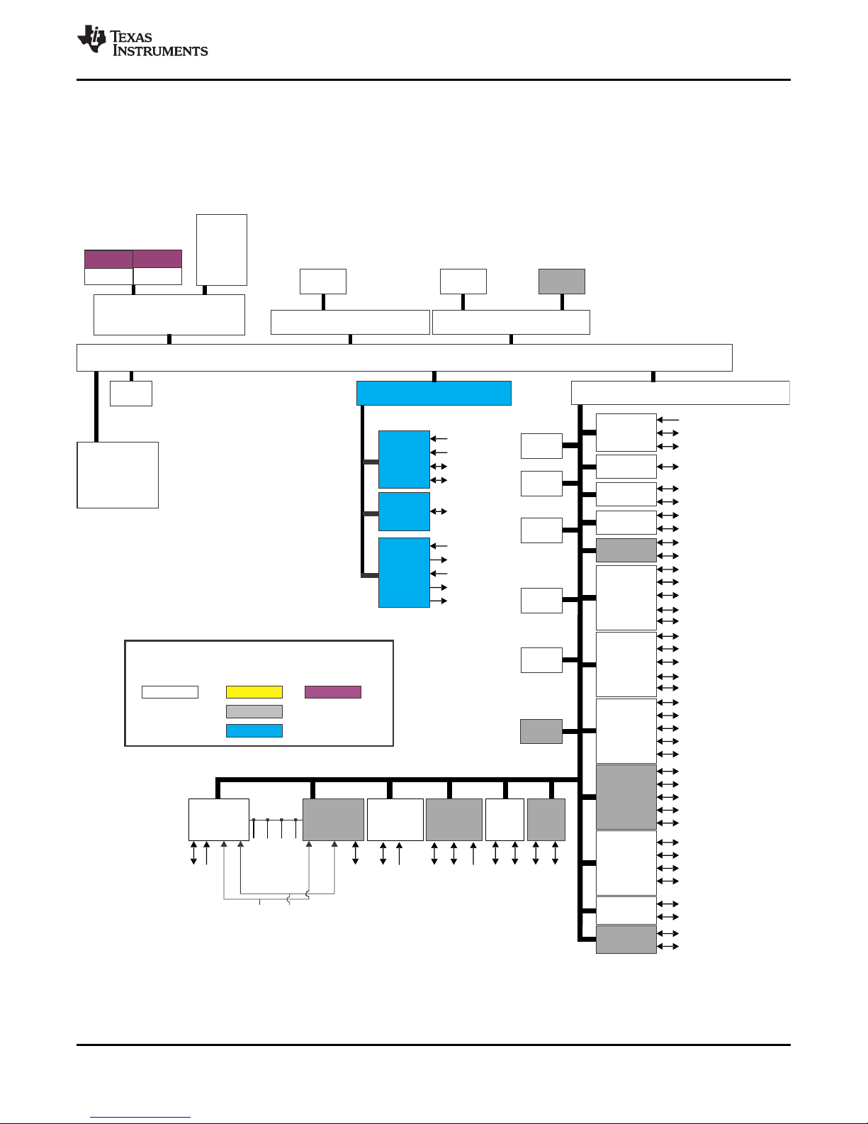
1.4 Functional Block Diagram
Figure 1-1 shows the functional block diagram of the device.
NOTE: The block diagram reflects the 144PGE package. Some functions are multiplexed or not available
in other packages. For details, see the respective terminal functions table in Section 4.2, Terminal
Functions.
TMS570LS0714
SPNS226E –JUNE 2013–REVISED NOVEMBER 2016
Figure 1-1. Functional Block Diagram
Submit Documentation Feedback
Product Folder Links: TMS570LS0714
Device OverviewCopyright © 2013–2016, Texas Instruments Incorporated
5
Page 6

TMS570LS0714
SPNS226E –JUNE 2013–REVISED NOVEMBER 2016
www.ti.com
Table of Contents
1 Device Overview ......................................... 1
1.1 Features .............................................. 1
1.2 Applications........................................... 2
1.3 Description............................................ 3
1.4 Functional Block Diagram ............................ 5
2 Revision History ......................................... 7
3 Device Comparison ..................................... 8
3.1 Related Products ..................................... 8
4 Terminal Configuration and Functions.............. 9
4.1 Pin Diagrams ......................................... 9
4.2 Signal Descriptions ................................. 11
4.3 Pin Multiplexing...................................... 29
4.4 Buffer Type.......................................... 35
5 Specifications .......................................... 36
5.1 Absolute Maximum Ratings......................... 36
5.2 ESD Ratings ........................................ 36
5.3 Power-On Hours (POH)............................. 36
5.4 Recommended Operating Conditions............... 37
5.5 Input/Output Electrical Characteristics Over
Recommended Operating Conditions............... 38
5.6 Power Consumption Over Recommended
Operating Conditions................................ 39
5.7 Thermal Resistance Characteristics ................ 40
5.8 Timing and Switching Characteristics............... 41
6 System Information and Electrical
Specifications........................................... 43
6.1 Device Power Domains ............................. 43
6.2 Voltage Monitor Characteristics..................... 43
6.3 Power Sequencing and Power-On Reset ........... 44
6.4 Warm Reset (nRST)................................. 46
6.5 ARM Cortex-R4F CPU Information ................. 47
6.6 Clocks ............................................... 51
6.7 Clock Monitoring .................................... 58
6.8 Glitch Filters......................................... 60
6.9 Device Memory Map ................................ 61
6.10 Flash Memory ....................................... 66
6.11 Tightly Coupled RAM Interface Module ............. 69
6.12 Parity Protection for Accesses to Peripheral RAMs 69
6.13 On-Chip SRAM Initialization and Testing ........... 71
6.14 Vectored Interrupt Manager......................... 73
6.15 DMA Controller...................................... 76
6.16 Real-Time Interrupt Module......................... 78
6.17 Error Signaling Module.............................. 80
6.18 Reset/Abort/Error Sources .......................... 84
6.19 Digital Windowed Watchdog ........................ 87
6.20 Debug Subsystem................................... 88
7 Peripheral Information and Electrical
Specifications........................................... 93
7.1 I/O Timings ......................................... 93
7.2 Enhanced PWM Modules (ePWM).................. 96
7.3 Enhanced Capture Modules (eCAP)............... 102
7.4 Enhanced Quadrature Encoder (eQEP)........... 105
7.5 12-Bit Multibuffered Analog-to-Digital Converter
(MibADC)........................................... 108
7.6 General-Purpose Input/Output..................... 121
7.7 Enhanced High-End Timer (N2HET) .............. 122
7.8 Controller Area Network (DCAN) .................. 126
7.9 Local Interconnect Network Interface (LIN)........ 127
7.10 Serial Communication Interface (SCI) ............. 128
7.11 Inter-Integrated Circuit (I2C) Module .............. 129
7.12 Multibuffered / Standard Serial Peripheral
Interface............................................ 132
8 Applications, Implementation, and Layout ...... 144
8.1 TI Designs or Reference Designs ................. 144
9 Device and Documentation Support.............. 145
9.1 Getting Started and Next Steps ................... 145
9.2 Device and Development-Support Tool
Nomenclature ...................................... 145
9.3 Tools and Software ................................ 147
9.4 Documentation Support............................ 149
9.5 Community Resources............................. 149
9.6 Trademarks ........................................ 149
9.7 Electrostatic Discharge Caution ................... 150
9.8 Glossary............................................ 150
9.9 Device Identification................................ 151
9.10 Module Certifications............................... 152
10 Mechanical Packaging and Orderable
Information............................................. 157
10.1 Packaging Information ............................. 157
6
Table of Contents Copyright © 2013–2016, Texas Instruments Incorporated
Submit Documentation Feedback
Product Folder Links: TMS570LS0714
Page 7

TMS570LS0714
www.ti.com
SPNS226E –JUNE 2013–REVISED NOVEMBER 2016
2 Revision History
NOTE: Page numbers for previous revisions may differ from page numbers in the current version.
This data manual revision history highlights the technical changes made to the SPNS226D device-specific
data manual to make it an SPNS226E revision.
Scope: Applicable updates to the TMS570LS0714 device family, specifically relating to the
TMS570LS0714 devices (Silicon Revision A), which are now in the production data (PD) stage of
development have been incorporated.
Changes from September 15, 2015 to November 1, 2016 (from D Revision (September 2015) to E Revision) Page
• GLOBAL: PZ package is now fully qualified ...................................................................................... 1
• Section 1.1 (Features): Updated/Changed the GIO pin count in GIO bullet.................................................. 1
• Section 1.1: Updated/Changed the SPI features bullet.......................................................................... 1
• Section 3.1 (Related Products): Added new section. ............................................................................ 8
• Section 4.2 (Signal Descriptions): Updated/Changed reference to Technical Reference Manual ....................... 11
• Table 4-2 (PGE Enhanced High-End Timer Modules (N2HET)): Added a description for pins 14 and 55
(N2HET1_PIN_nDIS and N2HET2_PIN_nDIS, respectively).................................................................. 13
• Table 4-20 (PZ Enhanced High-End Timer Modules (N2HET)): Added Pin 10, GIOA[5] / INT[5] / EXTCLKIN
/EPWM1A/N2HET1_PIN_nDIS.................................................................................................... 22
• Table 6-20 (Device Memory Map): Updated/Changed the FRAME SIZE column value for "Flash Data Space
ECC" under Flash Module Bus2 Interface from "768KB" to "1MB"........................................................... 62
• Section 6.19 (Digital Windowed Watchdog): Added Figure 6-13, Digital Windowed Watchdog Example............... 87
• Table 7-11 (eCAPx Clock Enable Control): Updated/Changed "ePWM" to "eCAP" in MODULE INSTANCE
column............................................................................................................................... 103
• Table 7-15 (eQEPx Clock Enable Control): Updated/Changed "ePWM" to "eQEP" in MODULE INSTANCE
column............................................................................................................................... 106
• Table 7-20 (MibADC1 Trigger Event Hookup): Added lead-in paragraph referencing the table ........................ 108
• Table 7-21 (MibADC2 Event Trigger Hookup): Added lead-in paragraph referencing the table ........................ 110
• Figure 7-11 (ePWM1SOC1A Switch Implementation): Added missing ePWM1 SOC1A detailed switch
connection example and lead-in reference sentence......................................................................... 114
• Section 9.1 (Getting Started and Next Steps): Added new section......................................................... 145
• Section 9.2 (Device and Development-Support Tool Nomenclature): Moved subsection after "Getting Started
and Next Steps" subsection (new) .............................................................................................. 145
• Section 9.9.1 Added the address of the Device ID register. ................................................................. 151
Submit Documentation Feedback
Product Folder Links: TMS570LS0714
Revision HistoryCopyright © 2013–2016, Texas Instruments Incorporated
7
Page 8

TMS570LS0714
SPNS226E –JUNE 2013–REVISED NOVEMBER 2016
3 Device Comparison
Table 3-1 lists the features of the TMS570LS0714 devices.
Table 3-1. TMS570LS0714 Device Comparison
www.ti.com
FEATURES TMS570LS DEVICES
Generic Part Number 3137ZWT
Package 337 BGA 337BGA 144 QFP 144 QFP 100 QFP 100 QFP
CPU ARM Cortex-R4F ARM Cortex-R4F ARM Cortex-R4F ARM Cortex-R4F ARM Cortex-R4F ARM Cortex-R4
Frequency (MHz) 180 180 160 160 100 80
Flash (KB) 3072 1280 1024 768 768 384
RAM (KB) 256 192 128 128 128 32
Data Flash [EEPROM]
(KB)
EMAC 10/100 10/100 – – – –
FlexRay 2-ch 2-ch – – – –
CAN 3 3 3 3 2 2
MibADC
12-bit (Ch)
N2HET (Ch) 2 (44) 2 (44) 2 (40) 2 (40) 2 (21) 1 (19)
ePWM Channels – 14 14 14 8 –
eCAP Channels – 6 6 6 4 0
eQEP Channels – 2 2 2 1 2
MibSPI (CS) 3 (6 + 6 + 4) 3 (6 + 6 + 4) 3 (5 + 6 + 1) 3 (5 + 6 + 4) 2 (5 + 1) 1 (4)
SPI (CS) 2 (2 + 1) 2 (2 + 1) 1 (1) 1 (1) 1 (1) 2
SCI (LIN) 2 (1 with LIN) 2 (1 with LIN) 2 (1 with LIN) 2 (1 with LIN) 1 (with LIN) 1 (with LIN)
I2C 1 1 1 1 – –
GPIO (INT)
EMIF 16-bit data 16-bit data – – – –
ETM (Trace) 32-bit – – – – –
RTP/DMM YES – – – – –
Operating
Temperature
Core Supply (V) 1.14 V – 1.32 V 1.14 V – 1.32 V 1.14 V – 1.32 V 1.14 V – 1.32 V 1.14 V – 1.32 V 1.14 V – 1.32 V
I/O Supply (V) 3.0 V – 3.6 V 3.0 V – 3.6 V 3.0 V – 3.6 V 3.0 V – 3.6 V 3.0 V – 3.6 V 3.0 V – 3.6 V
120 (with 16 interrupt
-40ºC to 125ºC -40ºC to 125ºC -40ºC to 125ºC -40ºC to 125ºC -40ºC to 125ºC -40ºC to 125ºC
(1)
64 64 64 64 64 16
2 x (24ch) 2 x (24ch) 2 x (24ch) 2 x (24ch) 2 x (16ch) 1 x (16ch)
capable)
101 (with 16 interrupt
1227ZWT
capable)
(1)
64 (with 10 interrupt
0914PGE
capable)
(1)
0714PGE 0714PZ 0432PZ
64 (with 10 interrupt
capable)
45 (with 9 interrupt
capable)
45 (with 8 interrupt
capable)
(1) Bolding denotes a superset device. For additional device variants, see www.ti.com/tms570
3.1 Related Products
For information about other devices in this family of products or related products, see the following links.
Products for TMS570 16-Bit and 32-Bit MCUs
An expansive portfolio of software and pin-compatible high-performance ARM®Cortex®-R-based MCU
products from 80 MHz up to 300 MHz with on-chip features that prove a high level of diagnostic coverage,
as well as provide scalability to address a wide range of applications.
Companion Products for TMS570LS0714
Review products that are frequently purchased or used with this product.
8
Device Comparison Copyright © 2013–2016, Texas Instruments Incorporated
Submit Documentation Feedback
Product Folder Links: TMS570LS0714
Page 9

1
108
234
5
GIOA[1]
nTRST
109
144
110
111
112
113
114
115
116
117
118
119
120
121
AD1IN[10] / AD2IN[10]
122
123
124
125
126
127
128
129
130
131
132
133
134
135
136
137
138
139
140
141
142
143
72
71
70
69
68
67
66
65
64
63
62
61
60
59
58
57
56
55
54
53
52
51
50
49
48
47
46
45
44
43
42
41
40
39
38
37
678
9
10111213141516171819202122
232324252627272829303132333435
36
107
106
105
104
103
102
101
100
999897969594939291908988878685848382818079787776757473
GIOB[3]
GIOA[0]
N2HET1[11]
FLTP1
FLTP2
GIOA[2]
VCCIO
VSS
CAN3RX
CAN3TX
GIOA[5]
N2HET1[22]
GIOA[6]
VCC
OSCIN
Kelvin_GND
OSCOUT
VSS
GIOA[7]
N2HET1[01]
N2HET1[03]
N2HET1[0]
VCCIO
VSS
VSS
VCC
N2HET1[02]
N2HET1[05]
N2HET1[07]
TEST
N2HET1[09]
N2HET1[4]
MIBSPI3NCS[1]
N2HET1[06]
N2HET1[13]
MIBSPI1NCS[2]
N2HET1[15]
VCCIO
VSS
VSS
VCC
nPORRST
VSS
VCC
VCC
VSS
MIBSPI3SOMI
MIBSPI3SIMO
MIBSPI3CLK
MIBSPI3NENA
MIBSPI3NCS[0]
VSS
VCC
AD1IN[16] / AD2IN[0]
AD1IN[17] / AD2IN[01]
AD1IN[0]
AD1IN[07]
AD1IN[18] / AD2IN[02]
AD1IN[19] / AD2IN[03]
AD1IN[20] / AD2IN[04]
AD1IN[21] / AD2IN[05]
ADREFHI
ADREFLO
VSSAD
VCCAD
AD1IN[09] / AD2IN[09]
AD1IN[01]
AD1IN[02]
AD1IN[03]
AD1IN[11] / AD2IN[11]
AD1IN[04]
AD1IN[12] / AD2IN[12]
AD1IN[05]
AD1IN[13] / AD2IN[13]
AD1IN[06]
AD1IN[22] / AD2IN[06]
AD1IN[14] / AD2IN[14]
AD1IN[08] / AD2IN[08]
AD1IN[23] / AD2IN[07]
AD1IN[15] / AD2IN[15]
AD1EVT
VCC
VSS
CAN1TX
CAN1RX
N2HET1[24]
N2HET1[26]
MIBSPI1SIMO
MIBSPI1SOMI
MIBSPI1CLK
MIBSPI1NENA
MIBSPI5NENA
MIBSPI5SOMI[0]
MIBSPI5SIMO[0]
MIBSPI5CLK
VCC
VSS
VSS
VCCIO
N2HET1[08]
N2HET1[28]
TMS
TDI
TDO
TCK
RTCK
VCC
VSS
nRST
nERROR
N2HET1[10]
ECLK
VCCIO
VSS
VSS
VCC
N2HET1[12]
N2HET1[14]
GIOB[0]
N2HET1[30]
CAN2TX
CAN2RX
MIBSPI1NCS[1]
LINRX
LINTX
GIOB[1]
VCCP
VSS
VCCIO
VCC
VSS
N2HET1[16]
N2HET1[18]
N2HET1[20]
GIOB[2]
VCC
VSS
MIBSPI1NCS[0]
www.ti.com
4 Terminal Configuration and Functions
4.1 Pin Diagrams
4.1.1 PGE QFP Package Pinout (144-Pin)
TMS570LS0714
SPNS226E –JUNE 2013–REVISED NOVEMBER 2016
A. Pins can have multiplexed functions. Only the default function is shown in Figure 4-1.
Figure 4-1. PGE QFP Package Pinout (144-Pin)
Submit Documentation Feedback
Product Folder Links: TMS570LS0714
Terminal Configuration and FunctionsCopyright © 2013–2016, Texas Instruments Incorporated
9
Page 10

MIBSPI1nCS[1]
VCCP
LINRX
VCCIO
ECLK
RTCK
26
27
28
29
30
31
32
33
34
35
36
37
38
39
40
41
42
43
44
45
46
47
48
49
50
N2HET1[6]
MIBSPI1nCS[2]
VCCIO
VSS
VCC
nPORRST
VCC
VSS
MIBSPI3nENA
AD1IN[21]
TCK
MIBSPI3nCS[0]
MIBSPI1nCS[3]
AD1IN[0]
AD1IN[7]
AD1IN[20]
VSSAD/ADREFLO
AD1IN[9]
VCCAD/ADREFHI
AD1IN[1]
AD1IN[10]
VSS
VCC
CAN2RX
CAN2TX
VCC
VSS
nERROR
nRST
TDO
TDI
nTRST
VSS
LINTX
MIBSPI3CLK
ADEVT
VSS
CAN1T X
CAN1RX
MIBSPI1SOMI
MIBSPI1CLK
MIBSPI1nENA
SPI2SOMI
SPI2SIMO
SPI2CLK
MIBSPI1nCS
TMS
VCC
MIBSPI1SIMO
VCCIO
25
24
23
22
212019
18
17
16
15
14
13
12
11
10
9
876
5
4
3
2
1
51
52
54
55
56
57
58
59
606162
63
64
65
66
67
68
69
70
71
72
73
74
75
53
GIOA[3]/INT[3]
VSS
VCCIO
TEST
VSS
KELVIN_GND
OS CIN
VC C
GIOA[6]/INT[6]
GIOA[5]/INT[5]
GIOA[2]/INT[2]
FLTP2
FLTP1
GIOA[4]/INT[4]
OSCOUT
100
99
98
97
96
95
94
93
92
91
90
89
88
87
86
85
84
83
82
81
80
79
78
77
76
VSS
VC C
VSS
MIBSPI3SOMI
MIBSPI3SIMO
AD1IN[16]
AD1IN[17]
N2HET1[4]
N2HET1[2]
N2HET1[0]
N2HET1[22]
N2HET1[24]
N2HET1[10]
N2HET1[8]
N2HET1[14]
N2HET1[12]
N2HET1[16]
N2HET1[18]
SPI2nCS[0]
AD1IN[2]
AD1IN[3]
AD1IN[11]
AD1IN[8]
AD1IN[6]
AD1IN[4]
AD1IN[5]
TMS570LS0714
SPNS226E –JUNE 2013–REVISED NOVEMBER 2016
4.1.2 PZ QFP Package Pinout (100-Pin)
www.ti.com
10
Terminal Configuration and Functions Copyright © 2013–2016, Texas Instruments Incorporated
Figure 4-2. PZ QFP Package Pinout (100-Pin)
Submit Documentation Feedback
Product Folder Links: TMS570LS0714
Page 11

www.ti.com
4.2 Signal Descriptions
The signal descriptions section shows pin information in module function order per package.
Section 4.2.1 and Section 4.2.2 identify the external signal names, the associated pin or ball numbers
along with the mechanical package designator, the pin or ball type (Input, Output, I/O, Power, or Ground),
whether the pin or ball has any internal pullup/pulldown, whether the pin or ball can be configured as a
GIO, and a functional pin or ball description. The first signal name listed is the primary function for that
terminal (pin or ball). The signal name in Bold is the function being described. For information on how to
select between different multiplexed functions, see Section 4.3, Pin Multiplexing or see the I/O Multiplexing
and Control Module (IOMM) chapter of the TMS570LS09x/07x 16/32-Bit RISC Flash Microcontroller
Technical Reference Manual (SPNU607).
All I/O signals except nRST are configured as inputs while nPORRST is low and immediately
after nPORRST goes high.
All output-only signals are configured as high impedance while nPORRST is low, and are
configured as outputs immediately after nPORRST goes high.
While nPORRST is low, the input buffers are disabled, and the output buffers are high
impedance.
TMS570LS0714
SPNS226E –JUNE 2013–REVISED NOVEMBER 2016
NOTE
In the Terminal Functions tables of Section 4.2.1 and Section 4.2.2, the RESET PULL
STATE is the state of the pullup or pulldown while nPORRST is low and immediately after
nPORRST goes high. The default pull direction may change when software configures the
pin for an alternate function. The PULL TYPE is the type of pull asserted when the signal
name in bold is enabled for the given terminal.
Submit Documentation Feedback
Product Folder Links: TMS570LS0714
Terminal Configuration and FunctionsCopyright © 2013–2016, Texas Instruments Incorporated
11
Page 12

TMS570LS0714
SPNS226E –JUNE 2013–REVISED NOVEMBER 2016
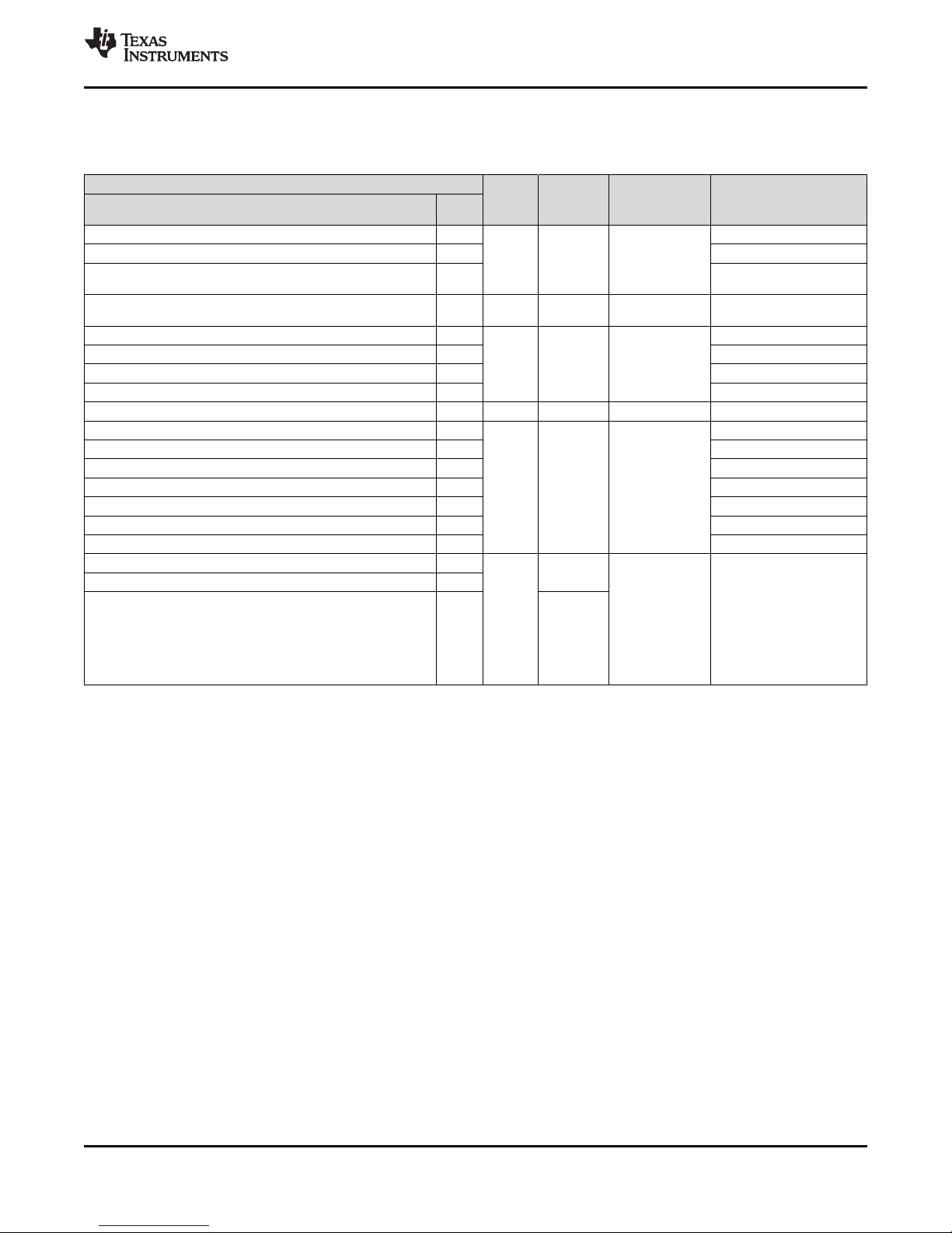
4.2.1 PGE Package Terminal Functions
4.2.1.1 Multibuffered Analog-to-Digital Converters (MibADCs)
Table 4-1. PGE Multibuffered Analog-to-Digital Converters (MibADC1, MibADC2)
www.ti.com
Terminal Signal
Signal Name 144
Type
Reset Pull
State
Pull Type Description
PGE
ADREFHI
(1)
66 Power – None ADC high reference
supply
ADREFLO
VCCAD
VSSAD
AD1EVT 86 I/O Pulldown Programmable,
MIBSPI3NCS[0]/AD2EVT/GIOB[2]/
EQEP1I/N2HET2_PIN_nDIS
(1)
(1)
(1)
67 Power ADC low reference supply
69 Power Operating supply for ADC
68 Ground
ADC1 event trigger input,
20 µA
55 I/O Pullup Programmable,
20 µA
or GIO
ADC2 event trigger input,
or GIO
AD1IN[0] 60 Input – None ADC1 analog input
AD1IN[01] 71
AD1IN[02] 73
AD1IN[03] 74
AD1IN[04] 76
AD1IN[05] 78
AD1IN[06] 80
AD1IN[07] 61
AD1IN[08] / AD2IN[08] 83 Input – None ADC1/ADC2 shared
AD1IN[09] / AD2IN[09] 70
analog inputs
AD1IN[10] / AD2IN[10] 72
AD1IN[11] / AD2IN[11] 75
AD1IN[12] / AD2IN[12] 77
AD1IN[13] / AD2IN[13] 79
AD1IN[14] / AD2IN[14] 82
AD1IN[15] / AD2IN[15] 85
AD1IN[16] / AD2IN[0] 58
AD1IN[17] / AD2IN[01] 59
AD1IN[18] / AD2IN[02] 62
AD1IN[19] / AD2IN[03] 63
AD1IN[20] / AD2IN[04] 64
AD1IN[21] / AD2IN[05] 65
AD1IN[22] / AD2IN[06] 81
AD1IN[23] / AD2IN[07] 84
MIBSPI3SOMI[0]/AWM1_EXT_ENA/ECAP2 51 Output Pullup – AWM1 external analog
mux enable
MIBSPI3SIMO[0]/AWM1_EXT_SEL[0]/ECAP3 52 Output Pullup – AWM1 external analog
mux select line0
MIBSPI3CLK/AWM1_EXT_SEL[1]/EQEP1A 53 Output Pullup – AWM1 external analog
mux select line0
(1) The ADREFHI, ADREFLO, VCCAD and VSSAD connections are common for both ADC cores.
12
Terminal Configuration and Functions Copyright © 2013–2016, Texas Instruments Incorporated
Submit Documentation Feedback
Product Folder Links: TMS570LS0714
Page 13

www.ti.com
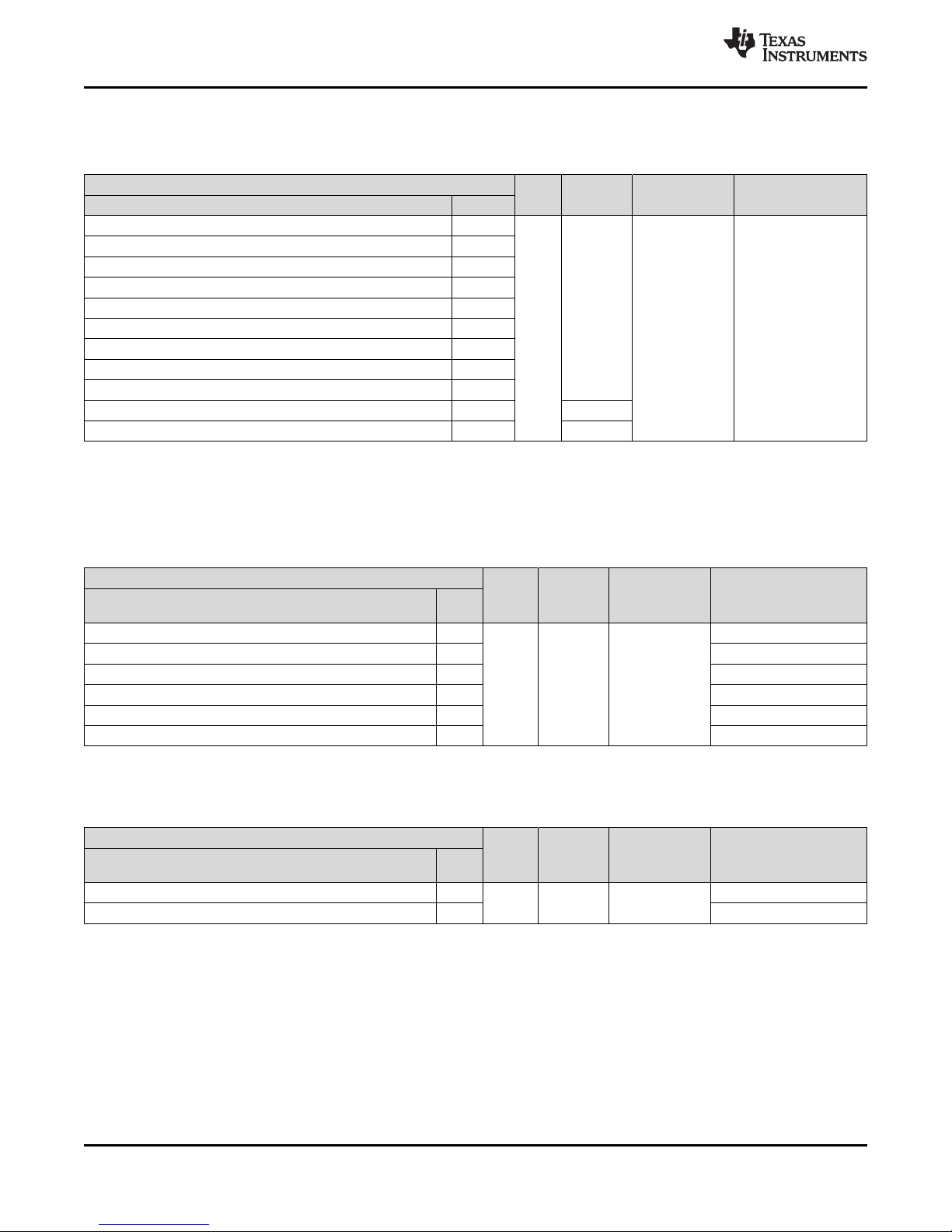
4.2.1.2 Enhanced High-End Timer (N2HET) Modules
Table 4-2. PGE Enhanced High-End Timer (N2HET) Modules
TERMINAL
SIGNAL NAME
N2HET1[0]/SPI4CLK/EPWM2B 25
N2HET1[01]/SPI4NENA/N2HET2[8]/EQEP2A 23
N2HET1[02]/SPI4SIMO[0]/EPWM3A 30
N2HET1[03]/SPI4NCS[0]/N2HET2[10]/EQEP2B 24
N2HET1[04]/EPWM4B 36
N2HET1[05]/SPI4SOMI[0]/N2HET2[12]/EPWM3B 31
N2HET1[06]/SCIRX/EPWM5A 38
N2HET1[07]/N2HET2[14]/EPWM7B 33
N2HET1[08]/MIBSPI1SIMO[1]/ 106
N2HET1[09]/N2HET2[16]/EPWM7A 35
N2HET1[10]/nTZ3 118
N2HET1[11]/MIBSPI3NCS[4]/N2HET2[18]/EPWM1SYNCO 6
N2HET1[12] 124
N2HET1[13]/SCITX/EPWM5B 39
N2HET1[14] 125
N2HET1[15]/MIBSPI1NCS[4]/ECAP1 41
N2HET1[16]/EPWM1SYNCI/EPWM1SYNCO 139
MIBSPI1NCS[1]/N2HET1[17]/EQEP1S 130 Pullup
N2HET1[18]/EPWM6A 140 Pulldown
MIBSPI1NCS[2]/N2HET1[19] 40 Pullup
N2HET1[20]/EPWM6B 141
N2HET1[22] 15
MIBSPI1NENA/N2HET1[23]/ECAP4 96 Pullup
N2HET1[24]/MIBSPI1NCS[5] 91 Pulldown
MIBSPI3NCS[1]/N2HET1[25] 37 Pullup
N2HET1[26] 92 Pulldown
MIBSPI3NCS[2]/I2CSDA/N2HET1[27]/nTZ2 4 Pullup
N2HET1[28] 107 Pulldown
MIBSPI3NCS[3]/I2CSCL/N2HET1[29]/nTZ1 3 Pullup
N2HET1[30]/EQEP2S 127 Pulldown
MIBSPI3NENA/MIBSPI3NCS[5]/N2HET1[31]/EQEP1B 54 Pullup
GIOA[5]/EXTCLKIN1/EPWM1A/N2HET1_PIN_nDIS 14 Pulldown
GIOA[2]/N2HET2[0]/EQEP2I 9
GIOA[6]/N2HET2[4]/EPWM1B 16
GIOA[7]/N2HET2[6]EPWM2A 22
N2HET1[01]/SPI4NENA//N2HET2[8] 23
N2HET1[03]/SPI4NCS[0]/N2HET2[10]/EQEP2B 24
N2HET1[05]/SPI4SOMI[0]/N2HET2[12]/EQEP3B 31
N2HET1[07]/N2HET2[14]/EPWM7B 33
N2HET1[09]/N2HET2[16] 35
N2HET1[11]/MIBSPI3NCS[4]/N2HET2[18]/EPWM1SYNCO 6
MIBSPI3NCS[0]/AD2EVT/GIOB[2]/EQEP1l/N2HET2_PIN_nDIS 55 Pullup
144
PGE
SIGNAL
TYPE
I/O
I/O
RESET
PULL
STATE
Pulldown
Pulldown
Pulldown
TMS570LS0714
SPNS226E –JUNE 2013–REVISED NOVEMBER 2016
DESCRIPTION
PULL TYPE
N2HET1 timer input
capture or output
compare, or GIO.
Programmable,
20 µA
Programmable,
20 µA
Each terminal has a
suppression filter with a
programmable duration.
Disable selected PWM
outputs
N2HET2 timer input
capture or output
compare, or GIO
Each terminal has a
suppression filter with a
programmable duration.
Disable selected PWM
outputs
Submit Documentation Feedback
Product Folder Links: TMS570LS0714
Terminal Configuration and FunctionsCopyright © 2013–2016, Texas Instruments Incorporated
13
Page 14

TMS570LS0714
SPNS226E –JUNE 2013–REVISED NOVEMBER 2016
4.2.1.3 Enhanced Capture Modules (eCAP)
www.ti.com
Table 4-3. PGE Enhanced Capture Modules (eCAP)
TERMINAL
SIGNAL NAME
N2HET1[15]/MIBSPI1NCS[4]/ECAP1 41
MIBSPI3SOMI[0]/AWM1_EXT_ENA/ECAP2 51
MIBSPI3SIMO[0]/AWM1_EXT_SEL[0]/ECAP3 52
MIBSPI1NENA/N2HET1[23]/ECAP4 96
MIBSPI5NENA/MIBSPI5SOMI[1]/ECAP5 97
MIBSPI1NCS[0]/MIBSPI1SOMI[1]/ECAP6 105
144
PGE
SIGNAL
TYPE
I/O
RESET
PULL
STATE
Pulldown
Pullup
(1)
PULL TYPE DESCRIPTION
Enhanced Capture Module 1
I/O
Enhanced Capture Module 2
I/O
Enhanced Capture Module 3
Fixed, 20 µA
I/O
Enhanced Capture Module 4
I/O
Enhanced Capture Module 5
I/O
Enhanced Capture Module 6
I/O
(1) These signals, when used as inputs, are double-synchronized and then optionally filtered with a 6-cycle VCLK4-based counter.
4.2.1.4 Enhanced Quadrature Encoder Pulse Modules (eQEP)
Table 4-4. PGE Enhanced Quadrature Encoder Pulse Modules (eQEP)
TERMINAL
SIGNAL NAME
MIBSPI3CLK/AWM1_EXT_SEL[1]/EQEP1A 53 Input
MIBSPI3NENA/MIBSPI3NCS[5]/N2HET1[31]/EQEP1B 54 Input Enhanced QEP1 Input B
MIBSPI3NCS[0]/AD2EVT/GIOB[2]/EQEP1I/N2HET2_PIN_nDIS 55 I/O Enhanced QEP1 Index
MIBSPI1NCS[1]/N2HET1[17]//EQEP1S 130 I/O Enhanced QEP1 Strobe
N2HET1[01]/SPI4NENA/N2HET2[8]/EQEP2A 23 Input
N2HET1[03]/SPI4NCS[0]/N2HET2[10]/EQEP2B 24 Input Enhanced QEP2 Input B
GIOA[2]/N2HET2[0]/EQEP2I 9 I/O EnhancedQEP2 Index
N2HET1[30]/EQEP2S 127 I/O Enhanced QEP2 Strobe
144
PGE
SIGNAL
TYPE
(1) These signals are double-synchronized and then optionally filtered with a 6-cycle VCLK4-based counter.
RESET
PULL
STATE
Pullup
Pulldown
PULL TYPE DESCRIPTION
Fixed, 20 µA
(1)
Enhanced QEP1 Input A
Enhanced QEP2 Input A
14
Terminal Configuration and Functions Copyright © 2013–2016, Texas Instruments Incorporated
Submit Documentation Feedback
Product Folder Links: TMS570LS0714
Page 15
TMS570LS0714
www.ti.com
SPNS226E –JUNE 2013–REVISED NOVEMBER 2016
4.2.1.5 Enhanced Pulse-Width Modulator Modules (ePWM)
Table 4-5. PGE Enhanced Pulse-Width Modulator Modules (ePWM)
TERMINAL
SIGNAL NAME
GIOA[5]/EXTCLKIN1/EPWM1A/N2HET1_PIN_nDIS 14
GIOA[6]/N2HET2[4]/EPWM1B 16 Enhanced PWM1 Output B
N2HET1[11]/MIBSPI3NCS[4]/N2HET2[18]/EPWM1SYNCO 6
N2HET1[16]/EPWM1SYNCI/EPWM1SYNCO 139 Input Pullup Fixed, 20 µA
GIOA[7]/N2HET2[6]/EPWM2A 22
N2HET1[0]/SPI4CLK/EPWM2B 25 Enhanced PWM2 Output B
N2HET1[02]/SPI4SIMO[0]/EPWM3A 30 Enhanced PWM3 Output A
N2HET1[05]/SPI4SOMI[0]/N2HET2[12]/EPWM3B 31 Enhanced PWM3 Output B
MIBSPI5NCS[0]/EPWM4A 32 Output Pullup – Enhanced PWM4 Output A
N2HET1[04]/EPWM4B 36
N2HET1[06]/SCIRX/EPWM5A 38 Enhanced PWM5 Output A
N2HET1[13]/SCITX/EPWM5B 39 Enhanced PWM5 Output B
N2HET1[18]/EPWM6A 140 Enhanced PWM6 Output A
N2HET1[20]/EPWM6B 141 Enhanced PWM6 Output B
N2HET1[09]/N2HET2[16]/EPWM7A 35 Enhanced PWM7 Output A
N2HET1[07]/N2HET2[14]/EPWM7B 33 Enhanced PWM7 Output B
MIBSPI3NCS[3]/I2CSCL/N2HET1[29]/nTZ1 3
MIBSPI3NCS[2]/I2CSDA/N2HET1[27]/nTZ2 4
N2HET1[10]/nTZ3 118 Pulldown
SIGNAL
144
PGE
TYPE
Output Pulldown –
Output Pulldown –
Output Pulldown –
Input
RESET
PULL
STATE
Pullup
PULL TYPE DESCRIPTION
Enhanced PWM1 Output A
External ePWM Sync Pulse
Output
External ePWM Sync Pulse
Output
Enhanced PWM2 Output A
Enhanced PWM4 Output B
Trip Zone Inputs 1, 2 and 3.
These signals are either
connected asynchronously to
the ePWMx trip zone inputs,
Fixed, 20 µA
or double-synchronized with
VCLK4, or doublesynchronized and then filtered
with a 6-cycle VCLK4-based
counter before connecting to
the ePWMx trip zone inputs.
Submit Documentation Feedback
Product Folder Links: TMS570LS0714
Terminal Configuration and FunctionsCopyright © 2013–2016, Texas Instruments Incorporated
15
Page 16
TMS570LS0714
SPNS226E –JUNE 2013–REVISED NOVEMBER 2016
4.2.1.6 General-Purpose Input/Output (GIO)
Table 4-6. PGE General-Purpose Input/Output (GIO)
www.ti.com
Terminal
Signal Name 144 PGE
GIOA[0] 2
GIOA[1] 5
GIOA[2]/N2HET2[0]/EQEPII 9
GIOA[5]/EXTCLKIN1/EPWM1A/N2HET1_PIN_nDIS 14
GIOA[6]/N2HET2[4]/EPWM1B 16
GIOA[7]/N2HET2[6]/EPWM2A 22
GIOB[0] 126
GIOB[1] 133
GIOB[2] 142
MIBSPI3NCS[0]/AD2EVT/GIOB[2]/EQEP1I/N2HET2_PIN_nDIS 55
GIOB[3] 1 Pulldown
(1) GIOB[2] cannot output a level on to pin 55. Only the input functionality is supported so that the application can generate an interrupt
whenever the N2HET2_PIN_nDIS is asserted (driven low). Also, a pullup is enabled on the input. This is not programmable using the
GIO module control registers.
Signal
(1)
Type
I/O
Reset Pull
State
Pulldown
Pullup
Pull Type Description
General-purpose I/O.
Programmable,
20 µA
All GIO terminals are
capable of generating
interrupts to the CPU
on rising / falling /
both edges.
4.2.1.7 Controller Area Network Controllers (DCAN)
Table 4-7. PGE Controller Area Network Controllers (DCAN)
Terminal Signal
Signal Name 144
PGE
CAN1RX 90 I/O Pullup Programmable,
CAN1TX 89 CAN1 transmit, or GIO
CAN2RX 129 CAN2 receive, or GIO
CAN2TX 128 CAN2 transmit, or GIO
CAN3RX 12 CAN3 receive, or GIO
CAN3TX 13 CAN3 transmit, or GIO
Type
Reset Pull
State
Pull Type Description
CAN1 receive, or GIO
20 µA
4.2.1.8 Local Interconnect Network Interface Module (LIN)
Table 4-8. PGE Local Interconnect Network Interface Module (LIN)
Terminal Signal
Signal Name 144
LINRX 131 I/O Pullup Programmable,
LINTX 132 LIN transmit, or GIO
16
Terminal Configuration and Functions Copyright © 2013–2016, Texas Instruments Incorporated
Type
PGE
Submit Documentation Feedback
Product Folder Links: TMS570LS0714
Reset Pull
State
Pull Type Description
LIN receive, or GIO
20 µA
Page 17

www.ti.com
4.2.1.9 Standard Serial Communication Interface (SCI)
Table 4-9. PGE Standard Serial Communication Interface (SCI)
TMS570LS0714
SPNS226E –JUNE 2013–REVISED NOVEMBER 2016
Terminal Signal
Signal Name 144
PGE
N2HET1[06]/SCIRX/EPWM5A 38 I/O Pulldown Programmable,
N2HET1[13]/SCITX/EPWM5B 39 SCI transmit, or GIO
Type
Reset Pull
State
Pull Type Description
SCI receive, or GIO
20 µA
4.2.1.10 Inter-Integrated Circuit Interface Module (I2C)
Table 4-10. PGE Inter-Integrated Circuit Interface Module (I2C)
Terminal Signal
Signal Name 144
PGE
MIBSPI3NCS[2]/I2CSDA/N2HET1[27]/nTZ2 4 I/O Pullup Programmable,
MIBSPI3NCS[3]/I2CSCL/N2HET1[29]/nTZ1 3 I2C serial clock, or GIO
Type
Reset Pull
State
Pull Type Description
I2C serial data, or GIO
20 µA
4.2.1.11 Standard Serial Peripheral Interface (SPI)
Table 4-11. PGE Standard Serial Peripheral Interface (SPI)
Terminal Signal
Signal Name 144
PGE
N2HET1[0]/SPI4CLK/EPWM2B 25 I/O Pulldown Programmable,
N2HET1[03]/SPI4NCS[0]/N2HET2[10]/EQEP2B 24 SPI4 chip select, or GIO
N2HET1[01]/SPI4NENA/N2HET2[8]/EQEP2A 23 SPI4 enable, or GIO
N2HET1[02]/SPI4SIMO[0]/EPWM3A 30 SPI4 slave-input master-
N2HET1[05]/SPI4SOMI[0]/N2HET2[12]/EPWM3B 31 SPI4 slave-output master-
Type
Reset Pull
State
Pull Type Description
SPI4 clock, or GIO
20 µA
output, or GIO
input, or GIO
Submit Documentation Feedback
Product Folder Links: TMS570LS0714
Terminal Configuration and FunctionsCopyright © 2013–2016, Texas Instruments Incorporated
17
Page 18
TMS570LS0714
SPNS226E –JUNE 2013–REVISED NOVEMBER 2016
4.2.1.12 Multibuffered Serial Peripheral Interface Modules (MibSPI)
Table 4-12. PGE Multibuffered Serial Peripheral Interface Modules (MibSPI)
www.ti.com
Terminal Signal
Signal Name 144
PGE
MIBSPI1CLK 95 I/O Pullup Programmable,
MIBSPI1NCS[0]/MIBSPI1SOMI[1]/ECAP6 105 MibSPI1 chip select, or
MIBSPI1NCS[1]/N2HET1[17]//EQEP1S 130
MIBSPI1NCS[2]/N2HET1[19]/ 40
N2HET1[15]/MIBSPI1NCS[4]/ECAP1 41 Pulldown Programmable,
N2HET1[24]/MIBSPI1NCS[5] 91
MIBSPI1NENA/N2HET1[23]/ECAP4 96 Pullup Programmable,
MIBSPI1SIMO[0] 93 MibSPI1 slave-in master-
N2HET1[08]/MIBSPI1SIMO[1] 106 Pulldown Programmable,
MIBSPI1SOMI[0] 94 Pullup Programmable,
MIBSPI1NCS[0]/MIBSPI1SOMI[1]/ECAP6 105
MIBSPI3CLK/AWM1_EXT_SEL[1]/EQEP1A 53 I/O Pullup Programmable,
MIBSPI3NCS[0]/AD2EVT/GIOB[2]/EQEP1I/N2HET2_PIN_nDIS55 MibSPI3 chip select, or
MIBSPI3NCS[1]/N2HET1[25] 37
MIBSPI3NCS[2]/I2CSDA/N2HET1[27]/nTZ2 4
MIBSPI3NCS[3]/I2CSCL/N2HET1[29]/nTZ1 3
N2HET1[11]/MIBSPI3NCS[4]/N2HET2[18]/EPWM1SYNCO 6 Pulldown Programmable,
MIBSPI3NENA /MIBSPI3NCS[5]/N2HET1[31]/EQEP1B 54 Pullup Programmable,
MIBSPI3NENA/MIBSPI3NCS[5]/N2HET1[31]/EQEP1B 54 MibSPI3 enable, or GIO
MIBSPI3SIMO[0]/AWM1_EXT_SEL[0]/ECAP3 52 MibSPI3 slave-in master-
MIBSPI3SOMI[0]/AWM1_EXT_ENA/ECAP2 51 MibSPI3 slave-out master-
MIBSPI5CLK 100 I/O Pullup Programmable,
MIBSPI5NCS[0]/EPWM4A 32 MibSPI5 chip select, or
MIBSPI5NENA/MIBSPI5SOMI[1]/ECAP5 97 MibSPI5 enable, or GIO
MIBSPI5SIMO[0]/MIBSPI5SOMI[2] 99 MibSPI5 slave-in master-
MIBSPI5SOMI[0] 98 MibSPI5 slave-out master-
MIBSPI5NENA/MIBSPI5SOMI[1]/ECAP5 97 MibSPI5 SOMI[0], or GIO
MIBSPI5SIMO[0]/MIBSPI5SOMI[2] 99 MibSPI5 SOMI[0], or GIO
Type
Reset Pull
State
Pull Type Description
20 µA
20 µA
20 µA
20 µA
20 µA
20 µA
20 µA
20 µA
20 µA
MibSPI1 clock, or GIO
GIO
MibSPI1 chip select, or
GIO
MibSPI1 enable, or GIO
out, or GIO
MibSPI1 slave-in master-
out, or GIO
MibSPI1 slave-out master-
in, or GIO
MibSPI3 clock, or GIO
GIO
MibSPI3 chip select, or
GIO
MibSPI3 chip select, or
GIO
out, or GIO
in, or GIO
MibSPI5 clock, or GIO
GIO
out, or GIO
in, or GIO
18
Terminal Configuration and Functions Copyright © 2013–2016, Texas Instruments Incorporated
Submit Documentation Feedback
Product Folder Links: TMS570LS0714
Page 19

www.ti.com
SPNS226E –JUNE 2013–REVISED NOVEMBER 2016
4.2.1.13 System Module Interface
Table 4-13. PGE System Module Interface
TERMINAL
SIGNAL NAME
nPORRST 46 Input Pulldown 100 µA
nRST 116 I/O Pullup 100 µA
nERROR 117 I/O Pulldown 20 µA
144
PGE
SIGNAL
TYPE
RESET
PULL
STATE
PULL TYPE DESCRIPTION
TMS570LS0714
Power-on reset, cold reset
External power supply monitor
circuitry must drive nPORRST
low when any of the supplies
to the microcontroller fall out
of the specified range. This
terminal has a glitch filter.
See Section 6.8.
System reset, warm reset,
bidirectional.
The internal circuitry indicates
any reset condition by driving
nRST low.
The external circuitry can
assert a system reset by
driving nRST low. To ensure
that an external reset is not
arbitrarily generated, TI
recommends that an external
pullup resistor is connected to
this terminal.
This terminal has a glitch
filter. See Section 6.8.
ESM Error Signal
Indicates error of high
severity. See Section 6.8.
4.2.1.14 Clock Inputs and Outputs
Table 4-14. PGE Clock Inputs and Outputs
Terminal Signal
Signal Name 144
Type
PGE
OSCIN 18 Input – None From external
KELVIN_GND 19 Input Kelvin ground for oscillator
OSCOUT 20 Output To external
ECLK 119 I/O Pulldown Programmable,
GIOA[5]/EXTCLKIN1/EPWM1A /N2HET1_PIN_nDIS 14 Input Pulldown 20 µA External clock input #1
Reset Pull
State
Pull Type Description
crystal/resonator, or
external clock input
crystal/resonator
External prescaled clock
20 µA
output, or GIO.
Submit Documentation Feedback
Product Folder Links: TMS570LS0714
Terminal Configuration and FunctionsCopyright © 2013–2016, Texas Instruments Incorporated
19
Page 20

TMS570LS0714
SPNS226E –JUNE 2013–REVISED NOVEMBER 2016
4.2.1.15 Test and Debug Modules Interface
Table 4-15. PGE Test and Debug Modules Interface
www.ti.com
Terminal Signal
Signal Name 144
PGE
TEST 34 Input Pulldown Fixed, 100 µA Test enable. This terminal
nTRST 109 Input JTAG test hardware reset
RTCK 113 Output - None JTAG return test clock
TCK 112 Input Pulldown Fixed, 100 µA JTAG test clock
TDI 110 Input Pullup JTAG test data in
TDO 111 Output Pulldown JTAG test data out
TMS 108 Input Pullup JTAG test select
Type
Reset Pull
State
Pull Type Description
must be connected to
ground directly or via a
pulldown resistor.
4.2.1.16 Flash Supply and Test Pads
Table 4-16. PGE Flash Supply and Test Pads
Terminal Signal
Signal Name 144
PGE
VCCP 134 3.3-V
FLTP1 7 – – None Flash test pads. These
FLTP2 8
Type
Power
Reset Pull
State
– None Flash pump supply
Pull Type Description
terminals are reserved for
TI use only. For proper
operation these terminals
must connect only to a
test pad or not be
connected at all [no
connect (NC)].
4.2.1.17 Supply for Core Logic: 1.2V nominal
Table 4-17. PGE Supply for Core Logic: 1.2V nominal
Terminal Signal
Signal Name 144
VCC 17 1.2-V
VCC 29
VCC 45
VCC 48
VCC 49
VCC 57
VCC 87
VCC 101
VCC 114
VCC 123
VCC 137
VCC 143
20
Terminal Configuration and Functions Copyright © 2013–2016, Texas Instruments Incorporated
Submit Documentation Feedback
Product Folder Links: TMS570LS0714
PGE
Type
Power
Reset Pull
State
– None Core supply
Pull Type Description
Page 21

www.ti.com
4.2.1.18 Supply for I/O Cells: 3.3V nominal
Table 4-18. PGE Supply for I/O Cells: 3.3V nominal
TMS570LS0714
SPNS226E –JUNE 2013–REVISED NOVEMBER 2016
Terminal Signal
Signal Name 144
PGE
VCCIO 10 3.3-V
VCCIO 26
VCCIO 42
VCCIO 104
VCCIO 120
VCCIO 136
Type
Power
Reset Pull
State
– None Operating supply for I/Os
Pull Type Description
4.2.1.19 Ground Reference for All Supplies Except VCCAD
Table 4-19. PGE Ground Reference for All Supplies Except VCCAD
Terminal Signal
Signal Name 144
PGE
VSS 11 Ground – None Ground reference
VSS 21
VSS 27
VSS 28
VSS 43
VSS 44
VSS 47
VSS 50
VSS 56
VSS 88
VSS 102
VSS 103
VSS 115
VSS 121
VSS 122
VSS 135
VSS 138
VSS 144
Type
Reset Pull
State
Pull Type Description
Submit Documentation Feedback
Product Folder Links: TMS570LS0714
Terminal Configuration and FunctionsCopyright © 2013–2016, Texas Instruments Incorporated
21
Page 22

TMS570LS0714
SPNS226E –JUNE 2013–REVISED NOVEMBER 2016
4.2.2 PZ Package Terminal Functions
4.2.2.1 High-End Timer (N2HET) Modules
Table 4-20. PZ Enhanced High-End Timer (N2HET) Modules
TERMINAL SIGNAL
SIGNAL NAME 100 PZ
N2HET1[0]/ SPI4CLK / EPWM2B 19 I/O Pulldown Programmable,
N2HET1[2] / SPI4SIMO / EPWM3A 22
N2HET1[4] / EPWM4B 25
N2HET1[6] / SCIRX / EPWM5A 26
N2HET1[8] / MIBSPI1SIMO[1] 74
N2HET1[10] / nTZ3 83
N2HET1[12] 89
N2HET1[14] 90
N2HET1[16] / EPWM1SYNCI /
EPWM1SYNCO
MIBSPI1nCS[1] / N2HET1[17] / EQEP1S 93 Pullup
N2HET1[18] / EPWM6A 98 Pulldown
MIBSPI1nCS[2] / N2HET1[19] 27 Pullup
MIBSPI1nCS[3] / N2HET1[21] 39
N2HET1[22] 11 Pulldown
MIBSPI1nENA / N2HET1[23] / ECAP4 68 Pullup
N2HET1[24] / MIBSPI1nCS[5] 64 Pulldown
MIBSPI3nENA / MIBSPI3nCS[5] /
N2HET1[31] / EQEP1B
GIOA[5] / INT[5] / EXTCLKIN
/EPWM1A/N2HET1_PIN_nDIS
GIOA[2] / INT[2] / N2HET2[0] / EQEP2I 5 Pulldown
GIOA[3] / INT[3] / N2HET2[2] 8
GIOA[6] / INT[6] / N2HET2[4] / EPWM1B 12
GIOA[7] / INT[7] / N2HET2[6] / EPWM2A 18
97
37 Pullup
10 Pulldown Disable selected PWM outputs
TYPE
RESET
PULL
STATE
PULL TYPE DESCRIPTION
20 µA
www.ti.com
N2HET2 timer input capture or output
compare, or GIO.
Each terminal has a suppression filter with a
programmable duration.
Timer input capture or output compare. The N2HET
applicable terminals can be programmed as
general-purpose input/output (GIO).
N2HET2 timer input capture or output
compare, or GIO.
Each terminal has a suppression filter with a
programmable duration.
Timer input capture or output compare. The N2HET
applicable terminals can be programmed as
general-purpose input/output (GIO).
4.2.2.2 Enhanced Capture Modules (eCAP)
Table 4-21. PZ Enhanced Capture Modules (eCAP)
Terminal Signal
Signal Name 100
MIBSPI3SOMI[0] /
AWM1_EXT_ENA / ECAP2
MIBSPI3SIMO[0] /
AWM1_EXT_SEL[0] / ECAP3
MIBSPI1NENA / N2HET1[23] /
ECAP4
MIBSPI1NCS[0] /
MIBSPI1SOMI[1] / ECAP6
22
Terminal Configuration and Functions Copyright © 2013–2016, Texas Instruments Incorporated
PZ
34 I/O Pullup Fixed, 20 µA Enhanced Capture Module 2 I/O
35 Enhanced Capture Module 3 I/O
68 Enhanced Capture Module 4 I/O
73 Enhanced Capture Module 6 I/O
Type
Reset Pull
State
Pull Type Description
Submit Documentation Feedback
Product Folder Links: TMS570LS0714
Page 23

www.ti.com
SPNS226E –JUNE 2013–REVISED NOVEMBER 2016
4.2.2.3 Enhanced Quadrature Encoder Pulse Modules (eQEP)
Table 4-22. PZ Enhanced Quadrature Encoder Pulse Modules (eQEP)
TERMINAL
SIGNAL NAME
MIBSPI3CLK / AWM1_EXT_SEL[1] /
EQEP1A
MIBSPI3nENA / MIBSPI3nCS[5] /
N2HET1[31] / EQEP1B
MIBSPI3nCS[0] / AD2EVT / GIOB[2]
/ EQEP1I/N2HET2_PIN_nDIS
MIBSPI1nCS[1] / N2HET1[17] /
EQEP1S
GIOA[2] / INT[2] / N2HET2[0] /
EQEP2I
SIGNAL
100 PZ
36 I/O Pullup Fixed, 20 µA Enhanced QEP1 Input A
37 Enhanced QEP1 Input B
38 Enhanced QEP1 Index
93 Enhanced QEP1 Strobe
5 Pulldown Enhanced QEP2 Index
TYPE
RESET
PULL
STATE
PULL TYPE DESCRIPTION
4.2.2.4 Enhanced Pulse-Width Modulator Modules (ePWM)
Table 4-23. PZ Enhanced Pulse-Width Modulator Modules (ePWM)
TERMINAL
SIGNAL NAME 100 PZ
GIOA[5] / INT[5] / EXTCLKIN /
EPWM1A/N2HET1_PIN_nDIS
GIOA[6] / INT[6] / N2HET2[4] /
EPWM1B
N2HET1[16] / EPWM1SYNCI /
EPWM1SYNCO
N2HET1[16] / EPWM1SYNCI /
EPWM1SYNCO
GIOA[7] / INT[7] / N2HET2[6] /
EPWM2A
N2HET1[0] / SPI4CLK / EPWM2B 19 Enhanced PWM2 Output B
N2HET1[2] / SPI4SIMO / EPWM3A 22 Enhanced PWM3 Output A
N2HET1[4] / EPWM4B 25 Enhanced PWM4 Output B
N2HET1[6] / SCIRX / EPWM5A 26 Enhanced PWM5 Output A
N2HET1[18] / EPWM6A 98 Enhanced PWM6 Output A
N2HET1[10] / nTZ3 83 Input Pulldown Trip Zone 1 input 3
SIGNAL
TYPE
10 Output Pulldown – Enhanced PWM1 Output A
12 Pulldown Enhanced PWM1 Output B
97 Input Pulldown Fixed, 20 µA External ePWM Sync Pulse Input
97 Output Pulldown – External ePWM Sync Pulse Output
18 Enhanced PWM2 Output A
RESET
PULL
STATE
PULL TYPE DESCRIPTION
TMS570LS0714
Submit Documentation Feedback
Product Folder Links: TMS570LS0714
Terminal Configuration and FunctionsCopyright © 2013–2016, Texas Instruments Incorporated
23
Page 24

TMS570LS0714
SPNS226E –JUNE 2013–REVISED NOVEMBER 2016
4.2.2.5 General-Purpose Input/Output (GIO)
Table 4-24. PZ General-Purpose Input/Output (GIO)
www.ti.com
Terminal Signal
Signal Name 100
GIOA[0] / INT[0] 1 I/O Pulldown Programmable,
GIOA[1] / INT[1] 2
GIOA[2] / INT[2] / N2HET2[0] /
EQEP2I
GIOA[3] / INT[3] / N2HET2[2] 8
GIOA[4]/ INT[4] 9
GIOA[5] / INT[5] / EXTCLKIN /
EPWM1A/ N2HET1_PIN_nDIS
GIOA[6] / INT[6] / N2HET2[4] /
EPWM1B
GIOA[7] / INT[7] / N2HET2[6] /
EPWM2A
MIBSPI3nCS[0] / AD2EVT /
GIOB[2] /
EQEP1I/N2HET2_PIN_nDIS
PZ
10
12
18
38 I/O General-purpose input/output
Type
5
Reset Pull
State
Pull Type Description
GIOA
20 µA
GIOB
General-purpose input/output
All GPIO terminals are capable of generating
interrupts to the CPU on rising/falling/both edges.
4.2.2.6 Controller Area Network Interface Modules (DCAN1, DCAN2)
Table 4-25. PZ Controller Area Network Interface Modules (DCAN1, DCAN2)
Terminal Signal
Signal Name 100
PZ
CAN1RX 63 I/O Pullup Programmable,
CAN1TX 62 CAN1 Transmit, or GPIO
CAN2RX 92 I/O Pullup Programmable,
CAN2TX 91 CAN2 Transmit, or GPIO
Type
Reset Pull
State
Pull Type Description
DCAN1
CAN1 Receive, or general-purpose I/O (GPIO)
20 µA
DCAN2
CAN2 Receive, or GPIO
20 µA
24
Terminal Configuration and Functions Copyright © 2013–2016, Texas Instruments Incorporated
Submit Documentation Feedback
Product Folder Links: TMS570LS0714
Page 25

TMS570LS0714
www.ti.com
SPNS226E –JUNE 2013–REVISED NOVEMBER 2016
4.2.2.7 Standard Serial Peripheral Interfaces (SPI2 and SPI4)
Table 4-26. PZ Standard Serial Peripheral Interfaces (SPI2 and SPI4)
Terminal Signal Type Reset Pull
Signal Name 100 PZ
SPI2CLK 71 I/O Pullup Programmable, 20 µA SPI2 Serial Clock, or GPIO
SPI2nCS[0] 23 SPI2 Chip Select, or GPIO
SPI2SIMO 70 SPI2 Slave-In-Master-Out, or GPIO
SPI2SOMI 69 SPI2 Slave-Out-Master-In, or GPIO
The drive strengths for the SPI2CLK, SPI2SIMO and SPI2SOMI signals are selected individually by configuring the respective SRS bits of the SPIPC9 register
fo SPI2.
SRS = 0 for 8mA drive (fast). This is the default mode as the SRS bits in the SPIPC9 register default to 0.
SRS = 1 for 2mA drive (slow)
N2HET1[0] / SPI4CLK / EPWM2B 19 I/O Pulldown Programmable, 20 µA SPI2 Serial Clock, or GPIO
N2HET1[2] / SPI4SIMO / EPWM3A 22 SPI2 Slave-In-Master-Out, or GPIO
State
Pull Type Description
SPI2
SPI4
4.2.2.8 Multibuffered Serial Peripheral Interface (MibSPI1 and MibSPI3)
Table 4-27. PZ Multibuffered Serial Peripheral Interface (MibSPI1 and MibSPI3)
Terminal Signal
Signal Name 100 PZ
MIBSPI1CLK 67 I/O Pullup Programmable, 20 µA MibSPI1 Serial Clock, or GPIO
MIBSPI1nCS[0]/MIBSPI1SOMI[1]/
ECAP6
MIBSPI1nCS[1]/N2HET1[17]/
EQEP1S
MIBSPI1nCS[2]/N2HET1[19] 27
MIBSPI1nCS[3]/N2HET1[21] 39
MIBSPI1nENA/N2HET1[23]/
ECAP4
MIBSPI1SIMO[0] 65 MibSPI1 Slave-In-Master-Out, or GPIO
N2HET1[8]/MIBSPI1SIMO[1] 74
MIBSPI1SOMI[0] 66 MibSPI1 Slave-Out-Master-In, or GPIO
MIBSPI1nCS[0]/MIBSPI1SOMI[1]/
ECAP6
MIBSPI3CLK/AWM1_EXT_SEL[1]/
EQEP1A
MIBSPI3nCS[0]/AD2EVT/GIOB[2]/
EQEP1I/N2HET2_PIN_nDIS
MIBSPI3nENA/MIBSPI3nCS[5]/
N2HET1[31]/EQEP1B
MIBSPI3nENA/MIBSPI3nCS[5]/
N2HET1[31]/EQEP1B
MIBSPI3SIMO[0]/AWM1_EXT_SEL[0]/
ECAP3
MIBSPI3SOMI[0]/AWM1_EXT_ENA/
ECAP2
73 MibSPI1 Chip Select, or GPIO
93
68 MibSPI1 Enable, or GPIO
73
36 I/O Pullup Programmable, 20 µA MibSPI3 Serial Clock, or GPIO
38 MibSPI3 Chip Select, or GPIO
37
37 MibSPI3 Enable, or GPIO
35 MibSPI3 Slave-In-Master-Out, or GPIO
34 MibSPI3 Slave-Out-Master-In, or GPIO
Type
Reset Pull
State
MibSPI1
MibSPI3
Pull Type Description
Submit Documentation Feedback
Product Folder Links: TMS570LS0714
Terminal Configuration and FunctionsCopyright © 2013–2016, Texas Instruments Incorporated
25
Page 26
TMS570LS0714
SPNS226E –JUNE 2013–REVISED NOVEMBER 2016
4.2.2.9 Local Interconnect Network Controller (LIN)
Table 4-28. PZ Local Interconnect Network Controller (LIN)
www.ti.com
TERMINAL
SIGNAL NAME 100 PZ
LINRX 94 I/O Pullup Programmable, 20 µA LIN Receive, or GPIO
LINTX 95 LIN Transmit, or GPIO
SIGNAL
TYPE
RESET
PULL
STATE
PULL TYPE DESCRIPTION
4.2.2.10 Multibuffered Analog-to-Digital Converter (MibADC)
Table 4-29. PZ Multibuffered Analog-to-Digital Converter (MibADC)
Terminal Signal
Signal Name 100
AD1EVT 58 I/O Pulldown Programmable,
AD1IN[0] 42 Input – – Analog Inputs
AD1IN[1] 49
AD1IN[2] 51
AD1IN[3] 52
AD1IN[4] 54
AD1IN[5] 55
AD1IN[6] 56
AD1IN[7] 43
AD1IN[8]/AD2IN[8] 57
AD1IN[9]/AD2IN[9] 48
AD1IN[10]/AD2IN[10] 50
AD1IN[11]/AD2IN[11] 53
AD1IN[16]/AD2IN[0] 40
AD1IN[17]/AD2IN[1] 41
AD1IN[20]/AD2IN[4] 44
AD1IN[21]/AD2IN[5] 45
ADREFHI/VCCAD 46 Input/
ADREFLO/VSSAD 47 Input/
MIBSPI3SOMI[0]/AWM1_EXT_
ENA/
ECAP2
MIBSPI3SIMO[0]/AWM1_EXT_
SEL[0]/
ECAP3
MIBSPI3CLK/AWM1_EXT_SEL
[1]/
EQEP1A
MIBSPI3nCS[0]/AD2EVT/GIOB[
2]/
EQEP1I/N2HET2_PIN_nDIS
PZ
34 AWM external analog mux enable
35 AWM external analog mux select line 0
36 AWM external analog mux select line1
38 I/O ADC2 Event Trigger or GPIO
Type
Power
Ground
Reset Pull
State
– – ADC High Reference Level/ADC Operating
– – ADC Low Reference Level/ADC Supply Ground
Pull Type Description
MibADC1
ADC1 Event Trigger or GPIO
20 µA
Supply
MibADC2
26
Terminal Configuration and Functions Copyright © 2013–2016, Texas Instruments Incorporated
Submit Documentation Feedback
Product Folder Links: TMS570LS0714
Page 27
TMS570LS0714
www.ti.com
SPNS226E –JUNE 2013–REVISED NOVEMBER 2016
4.2.2.11 System Module Interface
Table 4-30. PZ System Module Interface
TERMINAL
SIGNAL NAME 100 PZ
nPORRST 31 Input Pullup 100 µA
nRST 81 I/O Pullup 100 µA
nERROR 82 I/O Pulldown 20 µA
SIGNAL
TYPE
RESET
PULL
STATE
PULL TYPE DESCRIPTION
Power-on reset, cold reset External power supply
monitor circuitry must drive nPORRST low when any of
the supplies to the microcontroller fall out of the
specified range. This terminal has a glitch filter. See
Section 6.8.
The external circuitry can assert a system reset by
driving nRST low. To ensure that an external reset is not
arbitrarily generated, TI recommends that an external
pullup resistor is connected to this terminal. This
terminal has a glitch filter. See Section 6.8.
ESM Error Signal. Indicates error of high severity. See
Section 6.8.
4.2.2.12 Clock Inputs and Outputs
Table 4-31. PZ Clock Inputs and Outputs
TERMINAL
SIGNAL NAME 100 PZ
OSCIN 14 Input – – From external crystal/resonator, or external clock input
KELVIN_GND 15 Input – – Dedicated ground for oscillator
OSCOUT 16 Output – – To external crystal/resonator
ECLK 84 I/O Pulldown Programmable, 20 µA External prescaled clock output, or GIO.
GIOA[5]/INT[5]/EXTCLKIN/EPWM1A
/N2HET1_PIN_nDIS
SIGNAL
TYPE
10 Input Pulldown 20 µA External Clock In
RESET
PULL
STATE
PULL TYPE DESCRIPTION
Submit Documentation Feedback
Product Folder Links: TMS570LS0714
Terminal Configuration and FunctionsCopyright © 2013–2016, Texas Instruments Incorporated
27
Page 28

TMS570LS0714
SPNS226E –JUNE 2013–REVISED NOVEMBER 2016
4.2.2.13 Test and Debug Modules Interface
Table 4-32. PZ Test and Debug Modules Interface
TERMINAL
SIGNAL NAME 100 PZ
nTRST 76 Input Pulldown Fixed, 100 µA JTAG test hardware reset
RTCK 80 Output – – JTAG return test clock
TCK 79 Input Pulldown Fixed, 100 µA JTAG test clock
TDI 77 I/O Pullup Fixed, 100 µA JTAG test data in
TDO 78 I/O Pulldown Fixed, 100 µA JTAG test data out
TMS 75 I/O Pullup Fixed, 100 µA JTAG test select
TEST 24 I/O Pulldown Fixed, 100 µA
SIGNAL
TYPE
RESET
PULL
STATE
PULL TYPE DESCRIPTION
Test enable. This terminal must be connected to ground
directly or via a pulldown resistor.
4.2.2.14 Flash Supply and Test Pads
Table 4-33. PZ Flash Supply and Test Pads
www.ti.com
Terminal Signal
Signal Name 100
Type
Reset Pull
State
Pull Type Description
PZ
VCCP 96 3.3-V
Power
– – Flash external pump voltage (3.3 V). This
terminal is required for both Flash read and Flash
program and erase operations.
FLTP1 3 Input – – Flash Test Pins. For proper operation this
FLTP2 4 Input – –
terminal must connect only to a test pad or not be
connected at all [no connect (NC)].
The test pad must not be exposed in the final
product where it might be subjected to an ESD
event.
4.2.2.15 Supply for Core Logic: 1.2-V Nominal
Table 4-34. PZ Supply for Core Logic: 1.2-V Nominal
Terminal Signal
Signal Name 100
Type
PZ
VCC 13 1.2-V
VCC 21
Power
VCC 30
VCC 32
VCC 61
VCC 88
VCC 99
Reset Pull
Pull Type Description
State
– – Digital logic and RAM supply
4.2.2.16 Supply for I/O Cells: 3.3-V Nominal
Table 4-35. PZ Supply for I/O Cells: 3.3-V Nominal
Terminal Signal
Signal Name 100
VCCIO 6 3.3-V
VCCIO 28
VCCIO 60
VCCIO 85
28
Terminal Configuration and Functions Copyright © 2013–2016, Texas Instruments Incorporated
PZ
Type
Reset Pull
State
Pull Type Description
– – I/O Supply
Power
Submit Documentation Feedback
Product Folder Links: TMS570LS0714
Page 29

www.ti.com
4.2.2.17 Ground Reference for All Supplies Except VCCAD
Table 4-36. PZ Ground Reference for All Supplies Except VCCAD
TMS570LS0714
SPNS226E –JUNE 2013–REVISED NOVEMBER 2016
Terminal Signal
Signal Name 100
PZ
VSS 7 Ground – – Device Ground Reference. This is a single
VSS 17
VSS 20
VSS 29
VSS 33
VSS 59
VSS 72
VSS 86
VSS 87
VSS 100
Type
Reset Pull
State
Pull Type Description
ground reference for all supplies except for the
ADC Supply.
4.3 Pin Multiplexing
This microcontroller has several interfaces and uses extensive multiplexing to bring out the functions as
required by the target application. The multiplexing is mostly on the output signals. A few inputs are also
multiplexed to allow the same input signal to be driven in from a selected terminal.
4.3.1 Output Multiplexing
Table 4-37 and Table 4-38 show the pin multiplexing control x register (PINMMRx) and the associated bit
fields that control each pin mux function.
Submit Documentation Feedback
Product Folder Links: TMS570LS0714
Terminal Configuration and FunctionsCopyright © 2013–2016, Texas Instruments Incorporated
29
Page 30

Copyright © 2013–2016, Texas Instruments IncorporatedTerminal Configuration and Functions
Submit Documentation Feedback
Product Folder Links: TMS570LS0714
30
TMS570LS0714
SPNS226E –JUNE 2013–REVISED NOVEMBER 2016
www.ti.com
Table 4-37. Multiplexing for Outputs on 144-Pin PGE Package(1)
144-PIN
PGE
DEFAULT
FUNCTION
CTRL1 OPTION 2 CTRL2 OPTION 3 CTRL3 OPTION 4 CTRL4 OPTION 5 CTRL5 OPTION 6 CTRL6
86 AD1EVT 10[0]
2 GIOA[0] 0[8]
5 GIOA[1] 1[0]
9 GIOA[2] 2[0] N2HET2[0] 2[3] EQEP2I 2[4]
14 GIOA[5] 2[24] EXTCLKIN1 2[25] EPWM1A 2[26]
16 GIOA[6] 3[16] N2HET2[4] 3[17] EPWM1B 3[18]
22 GIOA[7] 4[0] N2HET2[6] 4[1] EPWM2A 4[2]
126 GIOB[0] 18[24]
133 GIOB[1] 21[8]
1 GIOB[3] 0[0]
105 MIBSPI1NCS[0] 13[24] MIBSPI1SOMI[1] 13[25] ECAP6 13[28]
130 MIBSPI1NCS[1] 20[16] N2HET1[17] 20[17] EQEP1S 20[20]
40 MIBSPI1NCS[2] 8[8] N2HET1[19] 8[9]
96 MIBSPI1NENA 12[16] N2HET1[23] 12[17] ECAP4 12[20]
53 MIBSPI3CLK 33[24] AWM1_EXT_SEL[1] 33[25] EQEP1A 33[26]
55 MIBSPI3NCS[0] 9[16] AD2EVT 9[17] GIOB[2] 9[18] EQEP1I 9[19]
37 MIBSPI3NCS[1] 7[8] N2HET1[25] 7[9]
4 MIBSPI3NCS[2] 0[24] I2C_SDA 0[25] N2HET1[27] 0[26] nTZ2 0[27]
3 MIBSPI3NCS[3] 0[16] I2C_SCL 0[17] N2HET1[29] 0[18] nTZ1 0[19]
54 MIBSPI3NENA 9[8] MIBSPI3NCS[5] 9[9] N2HET1[31] 9[10] EQEP1B 9[11]
52 MIBSPI3SIMO 33[16] AWM1_EXT_SEL[0] 33[17] ECAP3 33[18]
51 MIBSPI3SOMI 33[8] AWM1_EXT_ENA 33[9] ECAP2 33[10]
100 MIBSPI5CLK 13[16]
32 MIBSPI5NCS[0] 27[0] EPWM4A 27[2]
97 MIBSPI5NENA 12[24] MIBSPI5SOMI[1] 12[28] ECAP5 12[29]
99 MIBSPI5SIMO[0] 13[8] MIBSPI5SOMI[2] 13[12]
98 MIBSPI5SOMI[0] 13[0]
25 N2HET1[0] 5[0] SPI4CLK 5[1] EPWM2B 5[2]
23 N2HET1[01] 4[16] SPI4NENA 4[17] 4[19] N2HET2[8] 4[20] EQEP2A 4[21]
30 N2HET1[02] 5[8] SPI4SIMO 5[9] EPWM3A 5[10]
24 N2HET1[03] 4[24] SPI4NCS[0] 4[25] 4[27] N2HET2[10] 4[28] EQEP2B 4[29]
36 N2HET1[04] 33[0] EPWM4B 33[1]
31 N2HET1[05] 5[16] SPI4SOMI 5[17] N2HET2[12] 5[18] EPWM3B 5[19]
38 N2HET1[06] 7[16] SCIRX 7[17] EPWM5A 7[18]
33 N2HET1[07] 6[0] N2HET2[14] 6[3] EPWM7B 6[4]
Page 31
Copyright © 2013–2016, Texas Instruments Incorporated Terminal Configuration and Functions
Submit Documentation Feedback
Product Folder Links: TMS570LS0714
31
TMS570LS0714
www.ti.com
SPNS226E –JUNE 2013–REVISED NOVEMBER 2016
Table 4-37. Multiplexing for Outputs on 144-Pin PGE Package(1) (continued)
144-PIN
PGE
DEFAULT
FUNCTION
CTRL1 OPTION 2 CTRL2 OPTION 3 CTRL3 OPTION 4 CTRL4 OPTION 5 CTRL5 OPTION 6 CTRL6
106 N2HET1[08] 14[0] MIBSPI1SIMO[1] 14[1]
35 N2HET1[09] 6[16] N2HET2[16] 6[17] EPWM7A 6[20]
118 N2HET1[10] 17[0] nTZ3 17[4]
6 N2HET1[11] 1[8] MIBSPI3NCS[4] 1[9] N2HET2[18] 1[10] EPWM1SYNCO 1[13]
124 N2HET1[12] 17[16]
39 N2HET1[13] 8[0] SCITX 8[1] EPWM5B 8[2]
125 N2HET1[14] 18[8]
41 N2HET1[15] 8[16] MIBSPI1NCS[4] 8[17] ECAP1 8[18]
139 N2HET1[16] 34[0] EPWM1SYNCI 34[1] EPWM1SYNCO 34[2]
140 N2HET1[18] 34[8] EPWM6A 34[9]
141 N2HET1[20] 34[16] EPWM6B 34[17]
15 N2HET1[22] 3[8]
91 N2HET1[24] 11[24] MIBSPI1NCS[5] 11[25]
92 N2HET1[26] 12[0]
107 N2HET1[28] 14[8]
127 N2HET1[30] 19[8] EQEP2S 19[11]
(1) The CTRLx columns contain a value of type x[y], which indicates the pin multiplexing control x register (PINMMRx) and the associated bit field [y].
Page 32

Copyright © 2013–2016, Texas Instruments IncorporatedTerminal Configuration and Functions
Submit Documentation Feedback
Product Folder Links: TMS570LS0714
32
TMS570LS0714
SPNS226E –JUNE 2013–REVISED NOVEMBER 2016
www.ti.com
(1) The CTRLx columns contain a value of type x[y], which indicates the pin multiplexing control x register (PINMMRx) and the associated bit field [y].
Table 4-38. Multiplexing for Outputs on 100-Pin PZ Package
(1)
100-PINPZDEFAULT
FUNCTION
CTRL1 OPTION 2 CTRL2 OPTION 3 CTRL3 OPTION 4 CTRL4 OPTION 5 CTRL5 OPTION 6 CTRL6
2 GIOA[1]/INT[1] 1[0]
5 GIOA[2]/INT[2] 2[0] N2HET2[0] 2[3] EQEP2I 2[4]
10 GIOA[5]/INT[5] 2[24] EXTCLKIN1 2[25] EPWM1A 2[26]
12 GIOA[6]/INT[6] 3[16] N2HET2[4] 3[17] EPWM1B 3[18]
18 GIOA[7]/INT[7] 4[0] N2HET2[6] 4[1] EPWM2A 4[2]
73 MIBSPI1NCS[0] 13[24] MIBSPI1SOMI[1] 13[25] ECAP6 13[28]
93 MIBSPI1NCS[1] 20[16] N2HET1[17] 20[17] EQEP1S 20[20]
27 MIBSPI1NCS[2] 8[8] N2HET1[19] 8[9]
68 MIBSPI1NENA 12[16] N2HET1[23] 12[17] ECAP4 12[20]
36 MIBSPI3CLK 33[24] AWM1_EXT_SEL[1] 33[25] EQEP1A 33[26]
38 MIBSPI3NCS[0] 9[16] AD2EVT 9[17] GIOB[2] 9[18] EQEP1I 9[19]
37 MIBSPI3NENA 9[8] MIBSPI3NCS[5] 9[9] N2HET1[31] 9[10] EQEP1B 9[11]
35 MIBSPI3SIMO[0] 33[16] AWM1_EXT_SEL[0] 33[17] ECAP3 33[18]
34 MIBSPI3SOMI[0] 33[8] AWM1_EXT_ENA 33[9] ECAP2 33[10]
19 N2HET1[0] 5[0] SPI4CLK 5[1] EPWM2B 5[2]
22 N2HET1[02] 5[8] SPI4SIMO 5[9] EPWM3A 5[10]
25 N2HET1[04] 33[0] EPWM4B 33[1]
26 N2HET1[06] 7[16] SCIRX 7[17] EPWM5A 7[18]
74 N2HET1[08] 14[0] MIBSPI1SIMO[1] 14[1]
83 N2HET1[10] 17[0] nTZ3 17[4]
97 N2HET1[16] 34[0] EPWM1SYNCI 34[1] EPWM1SYNCO 34[2]
98 N2HET1[18] 34[8] EPWM6A 34[9]
64 N2HET1[24] 11[24] MIBSPI1NCS[5] 11[25]
Page 33

www.ti.com
4.3.2 Multiplexing of Inputs
Some signals are connected to more than one terminal, the inputs for these signals can come from any of
the terminals. A multiplexor is implemented to let the application choose the terminal that will be used,
providing the input signal is from among the available options.
TMS570LS0714
SPNS226E –JUNE 2013–REVISED NOVEMBER 2016
Submit Documentation Feedback
Product Folder Links: TMS570LS0714
Terminal Configuration and FunctionsCopyright © 2013–2016, Texas Instruments Incorporated
33
Page 34

Copyright © 2013–2016, Texas Instruments IncorporatedTerminal Configuration and Functions
Submit Documentation Feedback
Product Folder Links: TMS570LS0714
34
TMS570LS0714
SPNS226E –JUNE 2013–REVISED NOVEMBER 2016
www.ti.com
Table 4-39. Input Multiplexing and Control for All Packages [144-Pin PGE, and 100-Pin PZ](1)
SIGNAL
NAME
DEDICATED INPUTS MULTIPLEXED INPUTS
INPUT MULTIPLEXOR
CONTROL
INPUT PATH SELECTED
144 PGE 100 PZ 144 PGE 100 PZ BIT1 BIT2 DEDICATED, IF MUXED, IF
GIOB[2] 142 – 55 38 PINMUX29[16] PINMUX29[16] BIT1 = 0(3) BIT1 = 1(3)
N2HET1[17] – – 130 93 PINMUX20[17] PINMUX24[16] not(BIT1) or (BIT1 and BIT2) = 1 BIT1 and not(BIT2) = 1
N2HET1[19] – – 40 27 PINMUX8[9] PINMUX24[24] not(BIT1) or (BIT1 and BIT2) = 1 BIT1 and not(BIT2) = 1
N2HET1[21] – – – – PINMUX9[25] PINMUX25[0] not(BIT1) or (BIT1 and BIT2) = 1 BIT1 and not(BIT2) = 1
N2HET1[23] – – 96 68 PINMUX12[17] PINMUX25[8] not(BIT1) or (BIT1 and BIT2) = 1 BIT1 and not(BIT2) = 1
N2HET1[25] – – 37 – PINMUX7[9] PINMUX25[16] not(BIT1) or (BIT1 and BIT2) = 1 BIT1 and not(BIT2) = 1
N2HET1[27] – – 4 – PINMUX0[26] PINMUX25[24] not(BIT1) or (BIT1 and BIT2) = 1 BIT1 and not(BIT2) = 1
N2HET1[29] – – 3 – PINMUX0[18] PINMUX26[0] not(BIT1) or (BIT1 and BIT2) = 1 BIT1 and not(BIT2) = 1
N2HET1[31] – – 54 37 PINMUX9[10] PINMUX26[8] not(BIT1) or (BIT1 and BIT2) = 1 BIT1 and not(BIT2) = 1
(1) The default inputs to the modules are from the dedicated input terminals. The application must configure the PINMUX registers as shown in order to select the multiplexed input path, if
required.
(2) The SPI4CLK, SPI4SIMO, SPI4SOMI, SPI4nENA and SPI4nCS[0] signals do not have a dedicated signal pad on this device. Therefore, the input multiplexors on these inputs are not
required. The control registers are still available to maintain compatibility to the emulation device.
(3) When the muxed input is selected for GIOB[2], the PINMUX9[16] and PINMUX9[17] must be cleared. These bits affect the control over the PULDIS (pull disable) and PSEL (pull select).
When the multiplexed input path is selected for GIOB[2], the PULDIS is tied to 0 (pull is enabled, cannot be disabled) and the PULSEL is tied to 1 (pull up selected, not programmable).
Page 35

www.ti.com
4.4 Buffer Type
TMS570LS0714
SPNS226E –JUNE 2013–REVISED NOVEMBER 2016
Table 4-40. Output Buffer Drive Strengths
Low-level Output Current, IOLfor VI= V
or
High-level Output Current, IOHfor VI= V
8mA
4mA
2mA zero-dominant
OLmax
OHmin
Signals
MIBSPI5CLK, MIBSPI5SOMI[0], MIBSPI5SOMI[1], MIBSPI5SOMI[2], MIBSPI5SOMI[3],
MIBSPI5SIMO[0], MIBSPI5SIMO[1], MIBSPI5SIMO[2], MIBSPI5SIMO[3],
TMS, TDI, TDO, RTCK,
SPI4CLK, SPI4SIMO, SPI4SOMI, SPI4NCS[0], SPI4NENA, nERROR,
N2HET2[1], N2HET2[3], N2HET2[5], N2HET2[7], N2HET2[9], N2HET2[11],
N2HET2[13], N2HET2[15]
ECAP1, ECAP4, ECAP5, ECAP6
EQEP1I, EQEP1S, EQEP2I, EQEP2S
EPWM1A, EPWM1B, EPWM1SYNCO, EPW2A, EPWM2B, EPWM3A, EPWM3B,
EPWM4A, EPWM4B, EPWM5A, EPWM5B, EPWM6A, EPWM6B, EPWM7A, EPWM7B
TEST,
MIBSPI3SOMI, MIBSPI3SIMO, MIBSPI3CLK, MIBSPI1SIMO, MIBSPI1SOMI,
MIBSPI1CLK,
ECAP2, ECAP3
nRST
AD1EVT,
CAN1RX, CAN1TX, CAN2RX, CAN2TX, CAN3RX, CAN3TX,
GIOA[0-7], GIOB[0-7],
LINRX, LINTX,
MIBSPI1NCS[0], MIBSPI1NCS[1-3], MIBSPI1NENA, MIBSPI3NCS[0-3],
MIBSPI3NENA, MIBSPI5NCS[0-3], MIBSPI5NENA,
N2HET1[0-31], N2HET2[0], N2HET2[2], N2HET2[4], N2HET2[6], N2HET2[8],
N2HET2[10], N2HET2[12], N2HET2[14], N2HET2[16], N2HET2[18],
ECLK,
selectable 8mA / 2mA
SPI2CLK, SPI2SIMO, SPI2SOMI
The default output buffer drive strength is 8mA for these signals.
Table 4-41. Selectable 8mA/2mA Control
SIGNAL CONTROL BIT ADDRESS 8mA (DEFAULT) 2mA
ECLK SYSPC10[0] 0xFFFF FF78 0 1
SPI2CLK SPI2PC9[9] 0xFFF7 F668 0 1
SPI2SIMO SPI2PC9[10] 0xFFF7 F668 0 1
SPI2SOMI SPI2PC9[11]
(1) Either SPI2PC9[11] or SPI2PC9[24] can change the output strength of the SPI2SOMI pin. In case of a 32-bit write where these two bits
differ, SPI2PC9[11] determines the drive strength.
(1)
Submit Documentation Feedback
Product Folder Links: TMS570LS0714
0xFFF7 F668 0 1
Terminal Configuration and FunctionsCopyright © 2013–2016, Texas Instruments Incorporated
35
Page 36

TMS570LS0714
SPNS226E –JUNE 2013–REVISED NOVEMBER 2016
5 Specifications
www.ti.com
5.1 Absolute Maximum Ratings
(1)
Over Operating Free-Air Temperature Range
MIN MAX UNIT
(2)
V
Supply voltage range:
Input voltage
CC
CCIO
V
CCAD
All input pins, with exception of ADC pins –0.3 4.6
ADC input pins –0.3 6.25
, V
(2)
CCP
(2)
Output voltage All output pins –0.3 4.6 V
IIK(VI< 0 or VI> V
All pins, except AD1IN[23:0] or AD2IN[15:0]
Input clamp current
AD1IN[23:0] or AD2IN[15:0]
CCIO
CCAD
)
)
Total –40 40
Output clamp current
IOK(VO< 0 or VO> V
All pins, except AWM1_EXT_x
CCIO
)
Total –40 40
Operating free-air
temperature (TA)
Operating junction
temperature (TJ)
Storage temperature (T
) –65 150 °C
stg
(1) Stresses beyond those listed under Absolute Maximum Ratings may cause permanent damage to the device. These are stress ratings
only, and functional operation of the device at these or any other conditions beyond those indicated under Recommended Operating
Conditions is not implied. Exposure to absolute-maximum-rated conditions for extended periods may affect device reliability.
(2) Maximum-rated conditions for extended periods may affect device reliability. All voltage values are with respect to their associated
grounds.
–0.3 1.43
–0.3 4.6
–0.3 6.25
–20 20
–10 10
–20 20
–40 125 °C
–40 150 °C
VV
V
mAIIK(VI< 0 or VI> V
mA
5.2 ESD Ratings
VALUE UNIT
Human Body Model (HBM), per AEC Q100-002
All pins ±500 V
V
(ESD)
Electrostatic discharge (ESD)
performance:
Charged Device Model (CDM),
per AEC Q100-011
100-pin PZ corner pins (1, 25, 26, 50,
51, 75, 76, 100)
144-pin PGE corner pins (1, 36, 37, 72,
73, 108, 109, 144)
(1) AEC Q100-002 indicates HBM stressing is done in accordance with the ANSI/ESDA/JEDEC JS‑001 specification.
5.3 Power-On Hours (POH)
NOMINAL CVDD VOLTAGE (V)
(1)(2)
JUNCTION
TEMPERATURE (Tj)
1.2 105ºC 100K
(1) This information is provided solely for your convenience and does not extend or modify the warranty provided under TI's standard terms
and conditions for TI semiconductor products.
(2) To avoid significant degradation, the device power-on hours (POH) must be limited to those specified in this table. To convert to
equivalent POH for a specific temperature profile, see the Calculating Equivalent Power-on-Hours for Hercules Safety MCUs Application
Report (SPNA207).
(1)
±2 kV
±750 V
±750 V
LIFETIME POH
36
Specifications Copyright © 2013–2016, Texas Instruments Incorporated
Submit Documentation Feedback
Product Folder Links: TMS570LS0714
Page 37

www.ti.com
TMS570LS0714
SPNS226E –JUNE 2013–REVISED NOVEMBER 2016
5.4 Recommended Operating Conditions
(1)
over operating free-air temperature range (unless otherwise noted)
TEST CONDITIONS MIN NOM MAX UNIT
V
CC
V
CCIO
V
CCAD
V
CCP
V
SS
V
SSAD
V
ADREFHI
V
ADREFLO
V
SLEW
V
hys
V
IL
V
IH
T
A
T
J
(1) All voltages are with respect to VSS, except V
(2) Reliability data is based upon a temperature profile that is equivalent to 100,000 power-on hours at 105°C junction temperature.
Digital logic supply voltage (Core) 1.14 1.2 1.32 V
Digital logic supply voltage (I/O) 3 3.3 3.6 V
MibADC supply voltage 3 5.25 V
Flash pump supply voltage 3 3.3 3.6 V
Digital logic supply ground 0 V
MibADC supply ground –0.1 0.1 V
Analog-to-digital high-voltage reference source V
Analog-to-digital low-voltage reference source V
Maximum positive slew rate for V
V
supplies
CPP
CCIO
, V
CCAD
and
SSAD
SSAD
V
V
CCAD
CCAD
Input hysteresis All inputs 180 mV
Low-level input voltage All inputs –0.3 0.8 V
High-level input voltage All inputs 2 V
CCIO
+ 0.3 V
Operating free-air temperature –40 125 °C
Operating junction temperature
(2)
, which is with respect to V
CCAD
SSAD
–40 150 °C
V
V
1 V/μs
Submit Documentation Feedback
Product Folder Links: TMS570LS0714
SpecificationsCopyright © 2013–2016, Texas Instruments Incorporated
37
Page 38
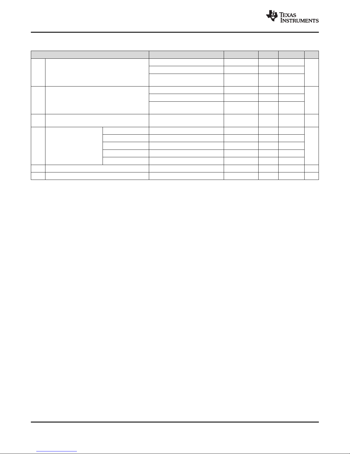
TMS570LS0714
SPNS226E –JUNE 2013–REVISED NOVEMBER 2016
www.ti.com
5.5 Input/Output Electrical Characteristics Over Recommended Operating Conditions
(1)
PARAMETER TEST CONDITIONS MIN TYP MAX UNIT
VOLLow-level output voltage
VOHHigh-level output voltage
I
Input clamp current (I/O pins)
IC
I
Input current (I/O pins)
I
IOL= I
IOL= 50 µA, standard output mode 0.2
IOL= 50 µA, low-EMI output mode
(see Section 7.1.2.1)
IOH= I
IOH= 50 µA, standard output mode V
IOH= 50 µA, low-EMI output mode
(see Section 7.1.2.1)
VI< V
VI> V
IIHPulldown 20 µA VI= V
IIHPulldown 100 µA VI= V
IILPullup 20 µA VI= V
IILPullup 100 µA VI= V
OLmax
OHmax
SSIO
CCIO
CCIO
CCIO
SS
SS
- 0.3 or
+ 0.3
0.8V
CCIO
- 0.3
CCIO
0.8V
CCIO
–3.5 3.5 mA
5 40
40 195
–40 –5
–195 –40
0.2V
0.2V
CCIO
CCIO
All other pins No pullup or pulldown –1 1
CIInput capacitance 2 pF
COOutput capacitance 3 pF
(1) Source currents (out of the device) are negative while sink currents (into the device) are positive.
V
V
µA
38
Specifications Copyright © 2013–2016, Texas Instruments Incorporated
Submit Documentation Feedback
Product Folder Links: TMS570LS0714
Page 39

TMS570LS0714
www.ti.com
SPNS226E –JUNE 2013–REVISED NOVEMBER 2016
5.6 Power Consumption Over Recommended Operating Conditions
PARAMETER TEST CONDITIONS MIN TYP MAX UNIT
I
CC
I
CCIO
VCCdigital supply current (operating mode)
f
= f
VCLK
V
CCmax
/2; Flash in pipelined mode;
HCLK
VCCdigital supply current (LBIST/PBIST mode)
V
digital supply current (operating mode) No DC load, V
CCIO
f
= 100 MHz 130
HCLK
f
= 160 MHz 160
HCLK
LBIST/PBIST clock
frequency = 50 MHz
LBIST/PBIST clock
frequency = 80 MHz
LBIST/PBIST clock
frequency = 90 MHz
CCmax
150
215
240
(1)
(1)
(1)
(1)
(1)
Single ADC
operational,
V
I
CCAD
V
supply current (operating mode)
CCAD
CCADmax
Both ADCs
operational,
V
CCADmax
Single ADC
operational,
AD
I
CCREFHI
AD
supply current (operating mode)
REFHI
REFHImax
Both ADCs
operational,
AD
REFHImax
Read from 1 bank
I
CCP
V
supply current
CCP
and program
another bank,
V
CCPmax
(1) The typical value is the average current for the nominal process corner and junction temperature of 25°C.
(2) The maximum I
• linearly with voltage
• by 0.85 mA/MHz for lower operating frequency when f
• for lower junction temperature by the equation below where TJKis the junction temperature in Kelvin and the result is in milliamperes.
126 - 0.005 e
(3) The maximum I
• linearly with voltage
value can be derated
CC,
0.024 T
JK
value can be derated
CC,
HCLK
= 2 * f
VCLK
• by 0.85 mA/MHz for lower operating frequency
• for lower junction temperature by the equation below where TJKis the junction temperature in Kelvin and the result is in milliamperes.
126 - 0.005 e
(4) LBIST and PBIST currents are for a short duration, typically less than 10 ms. They are usually ignored for thermal calculations for the
0.024 T
JK
device and the voltage regulator.
290
360
390
270
300
(3)(4)
(3)(4)
(3)(4)
(2)
mA
(2)
mA
15 mA
15
mA
30
3
mA
6
55 mA
Submit Documentation Feedback
Product Folder Links: TMS570LS0714
SpecificationsCopyright © 2013–2016, Texas Instruments Incorporated
39
Page 40

TMS570LS0714
SPNS226E –JUNE 2013–REVISED NOVEMBER 2016
5.7 Thermal Resistance Characteristics
Table 5-1 shows the thermal resistance characteristics for the QFP - PGE mechanical package.
Table 5-2 shows the thermal resistance characteristics for the QFP - PZ mechanical package.
Table 5-1. Thermal Resistance Characteristics (PGE Package)
RΘ
RΘ
RΘ
Ψ
RΘ
RΘ
RΘ
Ψ
JA
JB
JC
JT
Table 5-2. Thermal Resistance Characteristics (PZ Package)
JA
JB
JC
JT
Junction-to-free air thermal resistance, still
air using JEDEC 2S2P test board
Junction-to-board thermal resistance 19.7
Junction-to-case thermal resistance 9.4
Junction-to-package top, Still air 0.40
Junction-to-free air thermal resistance, still
air using JEDEC 2S2P test board
Junction-to-board thermal resistance 21.6
Junction-to-case thermal resistance 11.2
Junction-to-package top, Still air 0.50
www.ti.com
°C/W
37.5
°C/W
43.5
40
Specifications Copyright © 2013–2016, Texas Instruments Incorporated
Submit Documentation Feedback
Product Folder Links: TMS570LS0714
Page 41

TMS570LS0714
www.ti.com
SPNS226E –JUNE 2013–REVISED NOVEMBER 2016
5.8 Timing and Switching Characteristics
5.8.1 SYSCLK (Frequencies)
5.8.1.1 Switching Characteristics over Recommended Operating Conditions for Clock Domains
Table 5-3. Clock Domain Timing Specifications
PARAMETER DESCRIPTION CONDITIONS MIN MAX UNIT
Pipeline mode enabled 100
Pipeline mode disabled 45
Pipeline mode enabled 160
Pipeline mode disabled 50
HCLK
100 MHz
100 MHz
150 MHz
100 MHz
VCLK
f
HCLK
f
GCLK
f
VCLK
f
VCLK2
f
VCLK4
f
VCLKA1
f
RTICLK
PZ
HCLK - System clock frequency
PGE
GCLK - CPU clock frequency f
VCLK - Primary peripheral clock
frequency
VCLK2 - Secondary peripheral clock
frequency
VCLK4 - Secondary peripheral clock
frequency
VCLKA1 - Primary asynchronous
peripheral clock frequency
RTICLK - Clock frequency f
MHz
MHz
MHz
Submit Documentation Feedback
Product Folder Links: TMS570LS0714
SpecificationsCopyright © 2013–2016, Texas Instruments Incorporated
41
Page 42

Address Wait States
0 MHz f
HCLK(max)
Data Wait States
0 MHz f
HCLK(max)
Flash (Main Memory)
Address Wait States
0 MHz f
HCLK(max)
RWAIT Setting 0
0 MHz 50MHz f
HCLK(max)
Flash (Data Memory)
EWAIT Setting
2 3 4 5
0 MHz 45MHz 60MHz 75MHz 90MHz f
HCLK(max)
0
0
1
1
0
Address Wait States
0 MHz f
HCLK(max)
Data Wait States
0 MHz f
HCLK(max)
Flash (Main Memory)
Address Wait States
0 MHz 150MHz f
HCLK(max)
RWAIT Setting 0
0 MHz 50MHz f
HCLK(max)
Flash (Data Memory)
EWAIT Setting 2
3
4 5 6 7 8 9
0 MHz 45MHz 60MHz 75MHz 90MHz 105MHz 120MHz 135MHz 150MHz
0
0
1
0 1
2 31
100MHz 150MHz
f
HCLK(max)
TMS570LS0714
SPNS226E –JUNE 2013–REVISED NOVEMBER 2016
5.8.1.2 Wait States Required - PGE and PZ Packages
Figure 5-1. Wait States Scheme — PGE, 160 MHz
www.ti.com
Figure 5-2. Wait States Scheme — PZ, 100 MHz
As shown in Figure 5-1 and Figure 5-2, the TCM RAM can support program and data fetches at full CPU
speed without any address or data wait states required.
The TCM flash can support zero address and data wait states up to a CPU speed of 50 MHz in
nonpipelined mode. The flash supports a maximum CPU clock speed of 160 MHz in pipelined mode for
the PGE Package, and 100 MHz for the PZ package.
The flash wrapper defaults to nonpipelined mode with zero address wait state and one random-read data
wait state.
42
Specifications Copyright © 2013–2016, Texas Instruments Incorporated
Submit Documentation Feedback
Product Folder Links: TMS570LS0714
Page 43

www.ti.com
6 System Information and Electrical Specifications
6.1 Device Power Domains
The device core logic is split up into multiple power domains to optimize the power for a given application
use case. There are five core power domains: PD1, PD2, PD3, PD5, and RAM_PD1. See Section 1.4 for
more information.
PD1 is an "always-ON" power domain, which cannot be turned off. Each of the other core power domains
can be turned ON/OFF one time during device initialization as per the application requirement. Refer to
the Power Management Module (PMM) chapter of the device technical reference manual for more details.
NOTE
The clocks to a module must be turned off before powering down the core domain that
contains the module.
6.2 Voltage Monitor Characteristics
A voltage monitor is implemented on this device. The purpose of this voltage monitor is to eliminate the
requirement for a specific sequence when powering up the core and I/O voltage supplies.
6.2.1 Important Considerations
• The voltage monitor does not eliminate the need of a voltage supervisor circuit to ensure that the device is held in
reset when the voltage supplies are out of range.
• The voltage monitor only monitors the core supply (VCC) and the I/O supply (VCCIO). The other supplies are not
monitored by the VMON. For example, if the VCCAD or VCCP are supplied from a source different from that for
VCCIO, then there is no internal voltage monitor for the VCCAD and VCCP supplies.
TMS570LS0714
SPNS226E –JUNE 2013–REVISED NOVEMBER 2016
6.2.2 Voltage Monitor Operation
The voltage monitor generates the Power Good MCU signal (PGMCU) as well as the I/Os Power Good IO
signal (PGIO) on the device. During power-up or power-down, the PGMCU and PGIO are driven low when
the core or I/O supplies are lower than the specified minimum monitoring thresholds. The PGIO and
PGMCU signals being low isolates the core logic as well as the I/O controls during power up or power
down of the supplies. This allows the core and I/O supplies to be powered up or down in any order.
When the voltage monitor detects a low voltage on the I/O supply, it will assert a power-on reset. When
the voltage monitor detects an out-of-range voltage on the core supply, it asynchronously makes all output
pins high impedance, and asserts a power-on reset. The voltage monitor is disabled when the device
enters a low power mode.
The VMON also incorporates a glitch filter for the nPORRST input. Refer to Section 6.3.3.1 for the timing
information on this glitch filter.
Table 6-1. Voltage Monitoring Specifications
PARAMETER MIN TYP MAX UNIT
VCC low - VCC level below this
threshold is detected as too low.
V
MON
Voltage monitoring
thresholds
VCC high - VCC level above this
threshold is detected as too high.
VCCIO low - VCCIO level below this
threshold is detected as too low.
0.75 0.9 1.13
1.40 1.7 2.1
1.85 2.4 2.9
V
System Information and Electrical SpecificationsCopyright © 2013–2016, Texas Instruments Incorporated
Submit Documentation Feedback
Product Folder Links: TMS570LS0714
43
Page 44

TMS570LS0714
SPNS226E –JUNE 2013–REVISED NOVEMBER 2016
6.2.3 Supply Filtering
The VMON has the capability to filter glitches on the VCC and VCCIO supplies.
The following table shows the characteristics of the supply filtering. Glitches in the supply larger than the
maximum specification cannot be filtered.
Table 6-2. VMON Supply Glitch Filtering Capability
PARAMETER MIN MAX UNIT
Width of glitch on VCC that can be filtered 250 1000 ns
Width of glitch on VCCIO that can be filtered 250 1000 ns
6.3 Power Sequencing and Power-On Reset
6.3.1 Power-Up Sequence
There is no timing dependency between the ramp of the VCCIO and the VCC supply voltage. The powerup sequence starts with the I/O voltage rising above the minimum I/O supply threshold, (see Table 6-4 for
more details), core voltage rising above the minimum core supply threshold and the release of power-on
reset. The high-frequency oscillator will start up first and its amplitude will grow to an acceptable level. The
oscillator start-up time is dependent on the type of oscillator and is provided by the oscillator vendor. The
different supplies to the device can be powered up in any order.
www.ti.com
The device goes through the following sequential phases during power up.
Oscillator start-up and validity check 1032 oscillator cycles
eFuse autoload 1160 oscillator cycles
Flash pump power-up 688 oscillator cycles
Flash bank power-up 617 oscillator cycles
Total 3497 oscillator cycles
The CPU reset is released at the end of the above sequence and fetches the first instruction from address
0x00000000.
6.3.2 Power-Down Sequence
The different supplies to the device can be powered down in any order.
Table 6-3. Power-Up Phases
44
System Information and Electrical Specifications Copyright © 2013–2016, Texas Instruments Incorporated
Submit Documentation Feedback
Product Folder Links: TMS570LS0714
Page 45

3.3 V
1.2 V
V
CC
(1.2 V)
V
CCIO
/ V
CCP
(3.3 V)
8
6
3
7
6
9
V
CCPORH
V
CCIOPORL
V
IL(PORRST)
V
CCIOPORH
7
V
CCIOPORH
V
CCIOPORL
V
CCPORL
V
CC
nPORRST
V
CCIO
/ V
CCP
V
CCPORH
V
CCPORL
V
IL
V
IL
V
IL
V
IL
V
IL(PORRST)
TMS570LS0714
www.ti.com
SPNS226E –JUNE 2013–REVISED NOVEMBER 2016
6.3.3 Power-On Reset: nPORRST
This is the power-on reset. This reset must be asserted by an external circuitry whenever any power
supply is outside the specified recommended range. This signal has a glitch filter on it. It also has an
internal pulldown.
6.3.3.1 nPORRST Electrical and Timing Requirements
Table 6-4. Electrical Requirements for nPORRST
NO. MIN MAX UNIT
3 t
6 t
7 t
8 t
9 t
V
CCPORL
V
CCPORH
V
CCIOPORL
V
CCIOPORH
V
IL(PORRST)
su(PORRST)
h(PORRST)
su(PORRST)
h(PORRST)
h(PORRST)
VCClow supply level when nPORRST must be active during power up 0.5 V
VCChigh supply level when nPORRST must remain active during power
up and become active during power down
V
/ V
CCIO
power up
V
CCIO
during power up and become active during power down
Low-level input voltage of nPORRST V
Low-level input voltage of nPORRST V
Setup time, nPORRST active before V
power up
Hold time, nPORRST active after VCC> V
Setup time, nPORRST active before VCC< V
Hold time, nPORRST active after V
Hold time, nPORRST active after VCC< V
low supply level when nPORRST must be active during
CCP
/ V
high supply level when nPORRST must remain active
CCP
> 2.5 V 0.2 * V
CCIO
< 2.5 V 0.5 V
CCIO
and V
CCIO
CCIO
and V
CCPORH
CCPORH
CCP
CCPORL
CCP
> V
> V
CCIOPORL
during
during power down 2 µs
CCIOPORH
1.14 V
1.1 V
3.0 V
CCIO
0 ms
1 ms
1 ms
0 ms
V
t
f(nPORRST)
Filter time nPORRST pin;
pulses less than MIN will be filtered out, pulses greater than MAX will
generate a reset.
A. Figure 6-1 shows that there is no timing dependency between the ramp of the V
Figure 6-1. nPORRST Timing Diagram
475 2000 ns
and the VCCsupply voltages.
CCIO
(A)
System Information and Electrical SpecificationsCopyright © 2013–2016, Texas Instruments Incorporated
45
Submit Documentation Feedback
Product Folder Links: TMS570LS0714
Page 46

TMS570LS0714
SPNS226E –JUNE 2013–REVISED NOVEMBER 2016
www.ti.com
6.4 Warm Reset (nRST)
This is a bidirectional reset signal. The internal circuitry drives the signal low on detecting any device reset
condition. An external circuit can assert a device reset by forcing the signal low. On this terminal, the
output buffer is implemented as an open drain (drives low only). To ensure an external reset is not
arbitrarily generated, TI recommends that an external pullup resistor is connected to this terminal.
This terminal has a glitch filter. It also has an internal pullup
6.4.1 Causes of Warm Reset
Table 6-5. Causes of Warm Reset
DEVICE EVENT SYSTEM STATUS FLAG
Power-Up Reset Exception Status Register, bit 15
Oscillator fail Global Status Register, bit 0
PLL slip Global Status Register, bits 8 and 9
Watchdog exception / Debugger reset Exception Status Register, bit 13
CPU Reset (driven by the CPU STC) Exception Status Register, bit 5
Software Reset Exception Status Register, bit 4
External Reset Exception Status Register, bit 3
6.4.2 nRST Timing Requirements
Table 6-6. nRST Timing Requirements
Valid time, nRST active after nPORRST inactive 2256t
t
v(RST)
t
f(nRST)
(1) Specified values do not include rise/fall times. For rise and fall timings, see Table 7-2.
Valid time, nRST active (all other System reset
conditions)
Filter time nRST pin;
pulses less than MIN will be filtered out, pulses greater
than MAX will generate a reset
32t
(1)
MIN MAX UNIT
c(OSC)
ns
c(VCLK)
475 2000 ns
46
System Information and Electrical Specifications Copyright © 2013–2016, Texas Instruments Incorporated
Submit Documentation Feedback
Product Folder Links: TMS570LS0714
Page 47

www.ti.com
6.5 ARM Cortex-R4F CPU Information
6.5.1 Summary of ARM Cortex-R4F CPU Features
The features of the ARM Cortex-R4F CPU include:
• An integer unit with integral EmbeddedICE-RT logic.
• High-speed Advanced Microprocessor Bus Architecture (AMBA) Advanced eXtensible Interfaces (AXI)
for Level two (L2) master and slave interfaces.
• Floating-Point Coprocessor
• Dynamic branch prediction with a global history buffer, and a 4-entry return stack
• Low interrupt latency.
• Nonmaskable interrupt.
• A Harvard Level one (L1) memory system with:
– Tightly-Coupled Memory (TCM) interfaces with support for error correction or parity checking
memories
– ARMv7-R architecture Memory Protection Unit (MPU) with 12 regions
• Dual core logic for fault detection in safety-critical applications.
• An L2 memory interface:
– Single 64-bit master AXI interface
– 64-bit slave AXI interface to TCM RAM blocks
• A debug interface to a CoreSight Debug Access Port (DAP).
• Six Hardware Breakpoints
• Two Watchpoints
• A Performance Monitoring Unit (PMU).
• A Vectored Interrupt Controller (VIC) port.
TMS570LS0714
SPNS226E –JUNE 2013–REVISED NOVEMBER 2016
For more information on the ARM Cortex-R4F CPU, see www.arm.com.
6.5.2 ARM Cortex-R4F CPU Features Enabled by Software
The following CPU features are disabled on reset and must be enabled by the application if required.
• ECC On Tightly-Coupled Memory (TCM) Accesses
• Hardware Vectored Interrupt (VIC) Port
• Floating-Point Coprocessor
• Memory Protection Unit (MPU)
6.5.3 Dual Core Implementation
The device has two Cortex-R4F cores, where the output signals of both CPUs are compared in the CCMR4 unit. To avoid common mode impacts the signals of the CPUs to be compared are delayed by two
clock cycles as shown in Figure 6-2.
System Information and Electrical SpecificationsCopyright © 2013–2016, Texas Instruments Incorporated
Submit Documentation Feedback
Product Folder Links: TMS570LS0714
47
Page 48

North
Flip West
F
CPU 1 CPU 2
2cycledelay
2cycledelay
CCM-R4
CCM-R4
compare
CPU1CLK
CPU2CLK
compare
error
Input+Control
Output+Control
TMS570LS0714
SPNS226E –JUNE 2013–REVISED NOVEMBER 2016
www.ti.com
Figure 6-2. Dual Core Implementation
The CPUs have a diverse CPU placement given by following requirements:
• different orientation; for example, CPU1 = "north" orientation, CPU2 = "flip west" orientation
• dedicated guard ring for each CPU
Figure 6-3. Dual-CPU Orientation
6.5.4 Duplicate Clock Tree After GCLK
The CPU clock domain is split into two clock trees, one for each CPU, with the clock of the second CPU
running at the same frequency and in phase to the clock of CPU1. See Figure 6-2.
6.5.5 ARM Cortex-R4F CPU Compare Module (CCM) for Safety
This device has two ARM Cortex-R4F CPU cores, where the output signals of both CPUs are compared in
the CCM-R4 unit. To avoid common mode impacts the signals of the CPUs to be compared are delayed in
a different way as shown in Figure 6-2.
To avoid an erroneous CCM-R4 compare error, the application software must initialize the registers of
both CPUs before the registers are used, including function calls where the register values are pushed
onto the stack.
48
System Information and Electrical Specifications Copyright © 2013–2016, Texas Instruments Incorporated
Submit Documentation Feedback
Product Folder Links: TMS570LS0714
Page 49

www.ti.com
6.5.6 CPU Self-Test
The CPU STC (Self-Test Controller) is used to test the two Cortex-R4F CPU Cores using the
Deterministic Logic BIST Controller as the test engine.
The main features of the self-test controller are:
• Ability to divide the complete test run into independent test intervals
• Capable of running the complete test as well as running few intervals at a time
• Ability to continue from the last executed interval (test set) as well as ability to restart from the
beginning (First test set)
• Complete isolation of the self-tested CPU core from rest of the system during the self-test run
• Ability to capture the Failure interval number
• Time-out counter for the CPU self-test run as a fail-safe feature
6.5.6.1 Application Sequence for CPU Self-Test
1. Configure clock domain frequencies.
2. Select number of test intervals to be run.
3. Configure the time-out period for the self-test run.
4. Enable self-test.
5. Wait for CPU reset.
6. In the reset handler, read CPU self-test status to identify any failures.
7. Retrieve CPU state if required.
TMS570LS0714
SPNS226E –JUNE 2013–REVISED NOVEMBER 2016
For more information see the device Technical Reference Manual.
6.5.6.2 CPU Self-Test Clock Configuration
The maximum clock rate for the self-test is HCLKmax/2. The STCCLK is divided down from the CPU
clock. This divider is configured by the STCCLKDIV register at address 0xFFFFE108.
For more information see the device-specific Technical Reference Manual.
6.5.6.3 CPU Self-Test Coverage
Table 6-7 lists the CPU self-test coverage achieved for each self-test interval. It also lists the cumulative
test cycles. The test time can be calculated by multiplying the number of test cycles with the STC clock
period.
Table 6-7. CPU Self-Test Coverage
INTERVALS TEST COVERAGE, % STCCLK CYLCES
0 0 0
1 62.13 1365
2 70.09 2730
3 74.49 4095
4 77.28 5460
5 79.28 6825
6 80.90 8190
7 82.02 9555
8 83.10 10920
9 84.08 12285
10 84.87 13650
11 85.59 15015
12 86.11 16380
System Information and Electrical SpecificationsCopyright © 2013–2016, Texas Instruments Incorporated
Submit Documentation Feedback
Product Folder Links: TMS570LS0714
49
Page 50

TMS570LS0714
SPNS226E –JUNE 2013–REVISED NOVEMBER 2016
Table 6-7. CPU Self-Test Coverage (continued)
INTERVALS TEST COVERAGE, % STCCLK CYLCES
13 86.67 17745
14 87.16 19110
15 87.61 20475
16 87.98 21840
17 88.38 23205
18 88.69 24570
19 88.98 25935
20 89.28 27300
21 89.50 28665
22 89.76 30030
23 90.01 31395
24 90.21 32760
www.ti.com
50
System Information and Electrical Specifications Copyright © 2013–2016, Texas Instruments Incorporated
Submit Documentation Feedback
Product Folder Links: TMS570LS0714
Page 51

OSCIN
OSCOUT
C1
(see Note A)
C2
Crystal
(a)
OSCIN OSCOUT
(b)
External
(toggling 0 V to 3.3 V)
Clock Signal
Kelvin_GND
(see Note B)
www.ti.com
6.6 Clocks
6.6.1 Clock Sources
Table 6-8 lists the available clock sources on the device. Each clock source can be enabled or disabled
using the CSDISx registers in the system module. The clock source number in the table corresponds to
the control bit in the CSDISx register for that clock source.
Table 6-8 also shows the default state of each clock source.
TMS570LS0714
SPNS226E –JUNE 2013–REVISED NOVEMBER 2016
Table 6-8. Available Clock Sources
CLOCK
SOURCE NO.
0 OSCIN Main oscillator Enabled
1 PLL1 Output from PLL1 Disabled
2 Reserved Reserved Disabled
3 EXTCLKIN1 External clock input 1 Disabled
4 LFLPO Low-frequency output of internal reference oscillator Enabled
5 HFLPO
6 Reserved Reserved Disabled
7 EXTCLKIN2 External clock input 2 Disabled
6.6.1.1 Main Oscillator
The oscillator is enabled by connecting the appropriate fundamental resonator/crystal and load capacitors
across the external OSCIN and OSCOUT pins as shown in Figure 6-4. The oscillator is a single-stage
inverter held in bias by an integrated bias resistor. This resistor is disabled during leakage test
measurement and low power modes.
TI strongly encourages each customer to submit samples of the device to the
resonator/crystal vendors for validation. The vendors are equipped to determine which load
capacitors will best tune their resonator/crystal to the microcontroller device for optimum
start-up and operation over temperature and voltage extremes.
NAME DESCRIPTION DEFAULT STATE
High-frequency output of internal reference
oscillator
Enabled
NOTE
An external oscillator source can be used by connecting a 3.3-V clock signal to the OSCIN pin and leaving
the OSCOUT pin unconnected (open) as shown in Figure 6-4.
Figure 6-4. Recommended Crystal/Clock Connection
System Information and Electrical SpecificationsCopyright © 2013–2016, Texas Instruments Incorporated
Submit Documentation Feedback
Product Folder Links: TMS570LS0714
51
Page 52

BIAS_EN
Low-Power
Oscillator
LFEN
LF_TRIM
HFEN
LFLPO
HFLPO
HFLPO_VALID
nPORRST
TMS570LS0714
SPNS226E –JUNE 2013–REVISED NOVEMBER 2016
www.ti.com
6.6.1.1.1 Timing Requirements for Main Oscillator
Table 6-9. Timing Requirements for Main Oscillator
MIN NOM MAX UNIT
tc(OSC) Cycle time, OSCIN (when using a sine-wave input) 50 200 ns
tw(OSCIL)
tw(OSCIH)
Pulse duration, OSCIN low (when input to the OSCIN
is a square wave)
Pulse duration, OSCIN high (when input to the OSCIN
is a square wave)
15 ns
15 ns
6.6.1.2 Low-Power Oscillator
The Low-Power Oscillator (LPO) is comprised of two oscillators — HF LPO and LF LPO, in a single
macro.
6.6.1.2.1 Features
The main features of the LPO are:
• Supplies a clock at extremely low power for power-saving modes. This is connected as clock source 4
of the Global Clock Module (GCM).
• Supplies a high-frequency clock for non-timing-critical systems. This is connected as clock source 5 of
the GCM.
• Provides a comparison clock for the crystal oscillator failure detection circuit.
Figure 6-5 shows a block diagram of the internal reference oscillator. This is a low-power oscillator (LPO)
and provides two clock sources: one nominally 80 kHz and one nominally 10 MHz.
52
System Information and Electrical Specifications Copyright © 2013–2016, Texas Instruments Incorporated
Figure 6-5. LPO Block Diagram
Submit Documentation Feedback
Product Folder Links: TMS570LS0714
Page 53
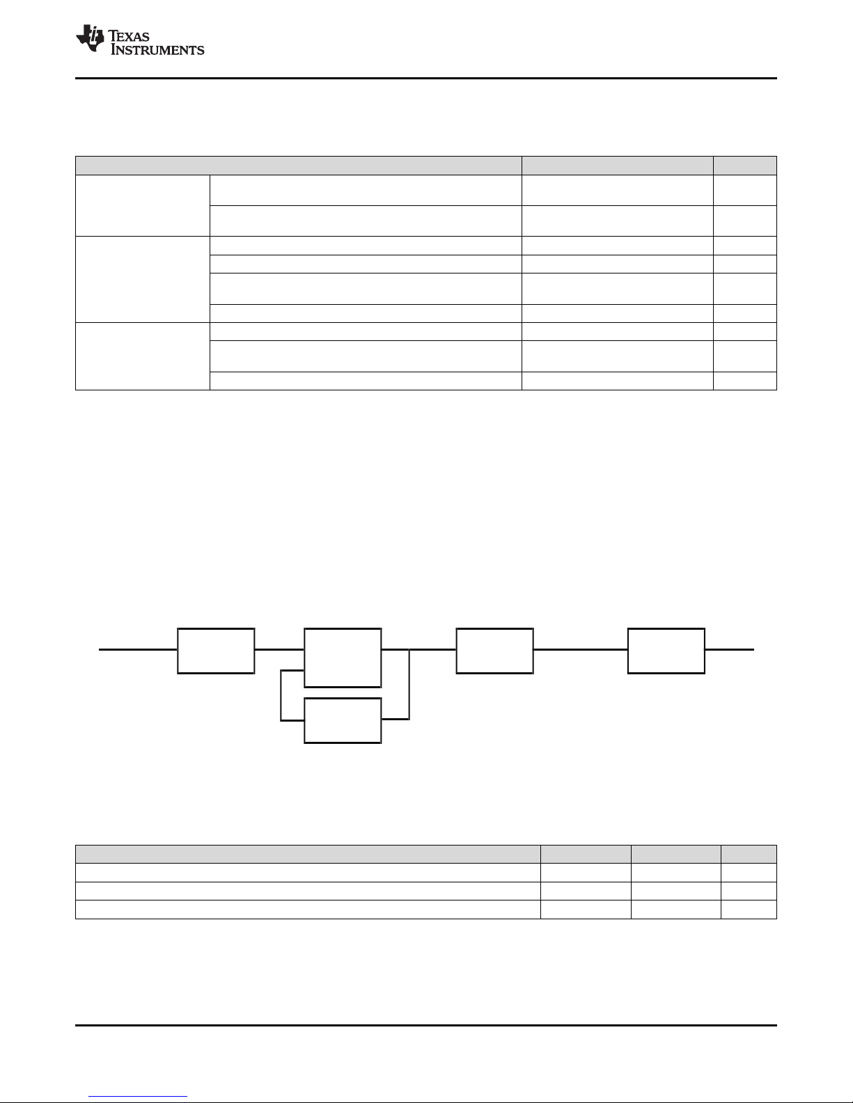
/NR
/1 to /64
OSCIN
PLL
INTCLK
/OD
/1 to /8
VCOCLK
/R
/1 to /32
post_ODCLK
/NF
/1 to /256
PLLCLK
f
PLLCLK
= (f
OSCIN
/ NR) * NF / (OD * R)
TMS570LS0714
www.ti.com
SPNS226E –JUNE 2013–REVISED NOVEMBER 2016
6.6.1.2.2 LPO Electrical and Timing Specifications
Table 6-10. LPO Specifications
PARAMETER MIN TYP MAX UNIT
Clock detection Oscillator fail frequency - lower threshold, using untrimmed
LPO output
Oscillator fail frequency - higher threshold, using untrimmed
LPO output
LPO - HF oscillator Untrimmed frequency 5.5 9 19.5 MHz
Trimmed frequency 8 9.6 11 MHz
Start-up time from STANDBY (LPO BIAS_EN high for at
least 900 µs)
Cold start-up time 900 µs
LPO - LF oscillator Untrimmed frequency 36 85 180 kHz
Start-up time from STANDBY (LPO BIAS_EN high for at
least 900 µs)
Cold start-up time 2000 µs
1.375 2.4 4.875 MHz
22 38.4 78 MHz
10 µs
100 µs
6.6.1.3 Phase-Locked Loop (PLL) Clock Module
The PLL is used to multiply the input frequency to some higher frequency.
The main features of the PLL are:
• Frequency modulation can be optionally superimposed on the synthesized frequency of PLL1.
• Configurable frequency multipliers and dividers
• Built-in PLL Slip monitoring circuit
• Option to reset the device on a PLL slip detection
6.6.1.3.1 Block Diagram
Figure 6-6 shows a high-level block diagram of the PLL macro on this microcontroller.
6.6.1.3.2 PLL Timing Specifications
Table 6-11. PLL Timing Specifications
PARAMETER MIN MAX UNIT
f
INTCLK
f
post_ODCLK
f
VCOCLK
PLL1 Reference Clock frequency 1 20 MHz
Post-ODCLK – PLL1 Post-divider input clock frequency 400 MHz
VCOCLK – PLL1 Output Divider (OD) input clock frequency 150 550 MHz
Figure 6-6. PLL Block Diagram
Submit Documentation Feedback
Product Folder Links: TMS570LS0714
System Information and Electrical SpecificationsCopyright © 2013–2016, Texas Instruments Incorporated
53
Page 54

TMS570LS0714
SPNS226E –JUNE 2013–REVISED NOVEMBER 2016
6.6.1.4 External Clock Inputs
The device supports up to two external clock inputs. This clock input must be a square-wave input.
Table 6-12 specifies the electrical and timing requirements for these clock inputs. The external clock
sources are not checked for validity. They are assumed valid when enabled.
Table 6-12. External Clock Timing and Electrical Specifications
PARAMETER MIN MAX UNIT
f
EXTCLKx
t
w(EXTCLKIN)H
t
w(EXTCLKIN)L
v
iL(EXTCLKIN)
v
iH(EXTCLKIN)
External clock input frequency 80 MHz
EXTCLK high-pulse duration 6 ns
EXTCLK low-pulse duration 6 ns
Low-level input voltage –0.3 0.8 V
High-level input voltage 2 VCCIO + 0.3 V
6.6.2 Clock Domains
6.6.2.1 Clock Domain Descriptions
Table 6-13 lists the device clock domains and their default clock sources. The table also shows the
system module control register that is used to select an available clock source for each clock domain.
www.ti.com
Table 6-13. Clock Domain Descriptions
CLOCK
DOMAIN
HCLK OSCIN GHVSRC
GCLK OSCIN GHVSRC
GCLK2 OSCIN GHVSRC
VCLK OSCIN GHVSRC
VCLK2 OSCIN GHVSRC
VCLK4 OSCIN GHVSRC
DEFAULT
SOURCE
SOURCE
SELECTION
REGISTER
SPECIAL CONSIDERATIONS
• Is disabled through the CDDISx registers bit 1
• Used for all system modules including DMA,
ESM
• Always the same frequency as HCLK
• In phase with HCLK
• Is disabled separately from HCLK through the
CDDISx registers bit 0
• Can be divided by 1 up to 8 when running CPU
self-test (LBIST) using the CLKDIV field of the
STCCLKDIV register at address 0xFFFFE108
• Always the same frequency as GCLK
• 2 cycles delayed from GCLK
• Is disabled along with GCLK
• Gets divided by the same divider setting as
that for GCLK when running CPU self-test
(LBIST)
• Divided down from HCLK
• Can be HCLK/1, HCLK/2, ... or HCLK/16
• Is disabled separately from HCLK through the
CDDISx registers bit 2
• Divided down from HCLK
• Can be HCLK/1, HCLK/2, ... or HCLK/16
• Frequency must be an integer multiple of
VCLK frequency
• Is disabled separately from HCLK through the
CDDISx registers bit 3
• Divided down from HCLK
• Can be HCLK/1, HCLK/2, ... or HCLK/16
• Is disabled separately from HCLK through the
CDDISx registers bit 9
54
System Information and Electrical Specifications Copyright © 2013–2016, Texas Instruments Incorporated
Submit Documentation Feedback
Product Folder Links: TMS570LS0714
Page 55

www.ti.com
Table 6-13. Clock Domain Descriptions (continued)
CLOCK
DOMAIN
VCLKA1 VCLK VCLKASRC
RTICLK VCLK RCLKSRC
DEFAULT
SOURCE
SOURCE
SELECTION
REGISTER
TMS570LS0714
SPNS226E –JUNE 2013–REVISED NOVEMBER 2016
SPECIAL CONSIDERATIONS
• Defaults to VCLK as the source
• Is disabled through the CDDISx registers bit 4
• Defaults to VCLK as the source
• If a clock source other than VCLK is selected
for RTICLK, then the RTICLK frequency must
be less than or equal to VCLK/3
– Application can ensure this by
programming the RTI1DIV field of the
RCLKSRC register, if necessary
• Is disabled through the CDDISx registers bit 6
System Information and Electrical SpecificationsCopyright © 2013–2016, Texas Instruments Incorporated
Submit Documentation Feedback
Product Folder Links: TMS570LS0714
55
Page 56

GCLK, GCLK2 (to CPU)
GCM
HCLK (to SYSTEM)
VCLK_peri (VCLK to peripherals on PCR1)
RTICLK (to RTI, DWWD)
/1, 2, 4, or 8
VCLK
OSCIN
Low-Power
Oscillator
10 MHz
80 kHz
1
0
4
5
/1..64
X1..256
/1..8
/1..32
6
*
VCLK
/1,2,..1024
Phase_seg2
CAN Baud Rate
Phase_seg1
VCLKA1
/1,2,..256
SPIx,MibSPIx
/2,3..2
24
LIN, SCI
SPI
LIN / SCI
/1,2..32
MibADCx
ADCLK
/1,2..65536
External Clock
ECLK
VCLK2
N2HETx
HRP
/1..64
LRP
/20..2
5
Loop
Resolution Clock
High
Baud Rate
Baud Rate
N2HETx
TU
VCLK2
EXTCLKIN1
EXTCLKIN2
3
7
0
1
4
5
6
3
7
VCLK_sys (VCLK to system modules)
* the frequency at this node must not
exceed the maximum HCLK specification.
/1,2..256
I2C
I2C baud
rate
NTU[1]
NTU[0]
NTU[2]
NTU[3]
RTI
Reserved
Reserved
Reserved
EXTCLKIN1
Prop_seg
DCANx
VCLK2 (to N2HETx and HTUx)
VCLKA1 (to DCANx)
0
1
4
5
6
VCLK
3
7
/1..16
/1..16
PLL #1 (FMzPLL)
VCLK4 (ePWM, eQEP, eCAP)
/1..16
Reserved
TMS570LS0714
SPNS226E –JUNE 2013–REVISED NOVEMBER 2016
6.6.2.2 Mapping of Clock Domains to Device Modules
Each clock domain has a dedicated functionality as shown in Figure 6-7 .
www.ti.com
Figure 6-7. Device Clock Domains
56
System Information and Electrical Specifications Copyright © 2013–2016, Texas Instruments Incorporated
Submit Documentation Feedback
Product Folder Links: TMS570LS0714
Page 57

www.ti.com
6.6.3 Clock Test Mode
The platform architecture defines a special mode that allows various clock signals to be selected and
output on the ECLK pin and N2HET1[12] device outputs. This special mode, Clock Test Mode, is very
useful for debugging purposes and can be configured through the CLKTEST register in the system
module. See Table 6-14 for the CLKTEST bits value and signal selection.
TMS570LS0714
SPNS226E –JUNE 2013–REVISED NOVEMBER 2016
Table 6-14. Clock Test Mode Options
SEL_ECP_PIN
=
CLKTEST[4-0]
00000 Oscillator 0000 Oscillator Valid Status
00001 Main PLL free-running clock output 0001 Main PLL Valid status
00010 Reserved 0010 Reserved
00011 EXTCLKIN1 0011 Reserved
00100 LFLPO 0100 Reserved
00101 HFLPO 0101 HFLPO Valid status
00110 Reserved 0110 Reserved
00111 EXTCLKIN2 0111 Reserved
01000 GCLK 1000 LFLPO
01001 RTI Base 1001 Oscillator Valid status
01010 Reserved 1010 Oscillator Valid status
01011 VCLKA1 1011 Oscillator Valid status
01100 VCLKA2 1100 Oscillator Valid status
01101 Reserved 1101 Reserved
01110 Reserved 1110 Reserved
01111 Reserved 1111 Oscillator Valid status
10000 Reserved
10001 HCLK
10010 VCLK
10011 VCLK2
10100 Reserved
10101 VCLK4
10110 Reserved
10111 Reserved
11000 Reserved
Others Reserved
SIGNAL ON ECLK
SEL_GIO_PIN
=
CLKTEST[11-8]
SIGNAL ON N2HET1[12]
System Information and Electrical SpecificationsCopyright © 2013–2016, Texas Instruments Incorporated
Submit Documentation Feedback
Product Folder Links: TMS570LS0714
57
Page 58
f[MHz]
1.375 4.875 22 78
fail
lower
threshold
pass
upper
threshold
fail
TMS570LS0714
SPNS226E –JUNE 2013–REVISED NOVEMBER 2016
6.7 Clock Monitoring
The LPO Clock Detect (LPOCLKDET) module consists of a clock monitor (CLKDET) and an internal LPO.
The LPO provides two different clock sources – a low frequency (LFLPO) and a high frequency (HFLPO).
The CLKDET is a supervisor circuit for an externally supplied clock signal (OSCIN). In case the OSCIN
frequency falls out of a frequency window, the CLKDET flags this condition in the global status register
(GLBSTAT bit 0: OSC FAIL) and switches all clock domains sourced by OSCIN to the HFLPO clock (limp
mode clock).
www.ti.com
The valid OSCIN frequency range is defined as: f
HFLPO
6.7.1 Clock Monitor Timings
For more information on LPO and Clock detection, see Table 6-10.
Figure 6-8. LPO and Clock Detection, Untrimmed HFLPO
6.7.2 External Clock (ECLK) Output Functionality
The ECLK pin can be configured to output a prescaled clock signal indicative of an internal device clock.
This output can be externally monitored as a safety diagnostic.
6.7.3 Dual Clock Comparators
The Dual Clock Comparator (DCC) module determines the accuracy of selectable clock sources by
counting the pulses of two independent clock sources (counter 0 and counter 1). If one clock is out of
spec, an error signal is generated. For example, the DCC1 can be configured to use HFLPO as the
reference clock (for counter 0) and VCLK as the "clock under test" (for counter 1). This configuration
allows the DCC1 to monitor the PLL output clock when VCLK is using the PLL output as its source.
/ 4 < f
OSCIN
< f
HFLPO
* 4.
An additional use of this module is to measure the frequency of a selectable clock source, using the input
clock as a reference, by counting the pulses of two independent clock sources. Counter 0 generates a
fixed-width counting window after a preprogrammed number of pulses. Counter 1 generates a fixed-width
pulse (1 cycle) after a preprogrammed number of pulses. This pulse sets as an error signal if counter 1
does not reach 0 within the counting window generated by counter 0.
6.7.3.1 Features
• Takes two different clock sources as input to two independent counter blocks.
• One of the clock sources is the known-good, or reference clock; the second clock source is the "clock under test."
• Each counter block is programmable with initial, or seed values.
• The counter blocks start counting down from their seed values at the same time; a mismatch from the expected
58
System Information and Electrical Specifications Copyright © 2013–2016, Texas Instruments Incorporated
frequency for the clock under test generates an error signal which is used to interrupt the CPU.
Submit Documentation Feedback
Product Folder Links: TMS570LS0714
Page 59
www.ti.com
6.7.3.2 Mapping of DCC Clock Source Inputs
Table 6-15. DCC1 Counter 0 Clock Sources
CLOCK SOURCE[3:0] CLOCK NAME
Others Oscillator (OSCIN)
0x5 High-frequency LPO
0xA Test clock (TCK)
Table 6-16. DCC1 Counter 1 Clock Sources
KEY[3:0] CLOCK SOURCE[3:0] CLOCK NAME
Others – N2HET1[31]
0xA 0x3 High-frequency LPO
SPNS226E –JUNE 2013–REVISED NOVEMBER 2016
0x0
0x1 Reserved
0x2 Low-frequency LPO
0x4 Reserved
0x5 EXTCLKIN1
0x6 EXTCLKIN2
0x7 Reserved
0x8 - 0xF VCLK
Main PLL free-running clock
output
TMS570LS0714
Table 6-17. DCC2 Counter 0 Clock Sources
CLOCK SOURCE [3:0] CLOCK NAME
Others Oscillator (OSCIN)
0xA Test clock (TCK)
Table 6-18. DCC2 Counter 1 Clock Sources
KEY [3:0] CLOCK SOURCE [3:0] CLOCK NAME
Others – N2HET2[0]
0xA 00x0 - 0x7 Reserved
0x8 - 0xF VCLK
System Information and Electrical SpecificationsCopyright © 2013–2016, Texas Instruments Incorporated
Submit Documentation Feedback
Product Folder Links: TMS570LS0714
59
Page 60

TMS570LS0714
SPNS226E –JUNE 2013–REVISED NOVEMBER 2016
6.8 Glitch Filters
A glitch filter is present on the following signals.
Table 6-19. Glitch Filter Timing Specifications
PIN PARAMETER MIN MAX UNIT
www.ti.com
nPORRST t
nRST t
TEST t
f(nPORRST)
f(nRST)
f(TEST)
Filter time nPORRST pin; pulses less than MIN will be filtered out, pulses
greater than MAX will generate a reset
(1)
Filter time nRST pin; pulses less than MIN will be filtered out, pulses
greater than MAX will generate a reset
Filter time TEST pin; pulses less than MIN will be filtered out, pulses
greater than MAX will pass through
475 2000 ns
475 2000 ns
475 2000 ns
(1) The glitch filter design on the nPORRST signal is designed such that no size pulse will reset any part of the microcontroller (flash pump,
I/O pins, and so forth) without also generating a valid reset signal to the CPU.
60
System Information and Electrical Specifications Copyright © 2013–2016, Texas Instruments Incorporated
Submit Documentation Feedback
Product Folder Links: TMS570LS0714
Page 61

Flash (768KB)
RAM (128KB)
0x00000000
CRC
Peripherals - Frame 1
SYSTEM Modules
0xFFFFFFFF
RAM - ECC
RESERVED
RESERVED
RESERVED
Flash (768KB) (Mirrored Image)
RESERVED
RESERVED
Peripherals - Frame 2
0xFFF80000
Flash Module Bus2 Interface
RESERVED
0x000BFFFF
0x08000000
0x0801FFFF
0xFE000000
0xFF000000
0xF07FFFFF
0x08400000
0x0841FFFF
0xF0000000
0x200BFFFF
0xFC000000
0x20000000
(Flash ECC, OTP and
EEPROM Emulation accesses)
www.ti.com
6.9 Device Memory Map
6.9.1 Memory Map Diagram
Figure 6-9 shows the device memory map.
TMS570LS0714
SPNS226E –JUNE 2013–REVISED NOVEMBER 2016
Figure 6-9. Memory Map
The Flash memory is mirrored to support ECC logic testing. The base address of the mirrored Flash
image is 0x2000 0000.
System Information and Electrical SpecificationsCopyright © 2013–2016, Texas Instruments Incorporated
Submit Documentation Feedback
Product Folder Links: TMS570LS0714
61
Page 62
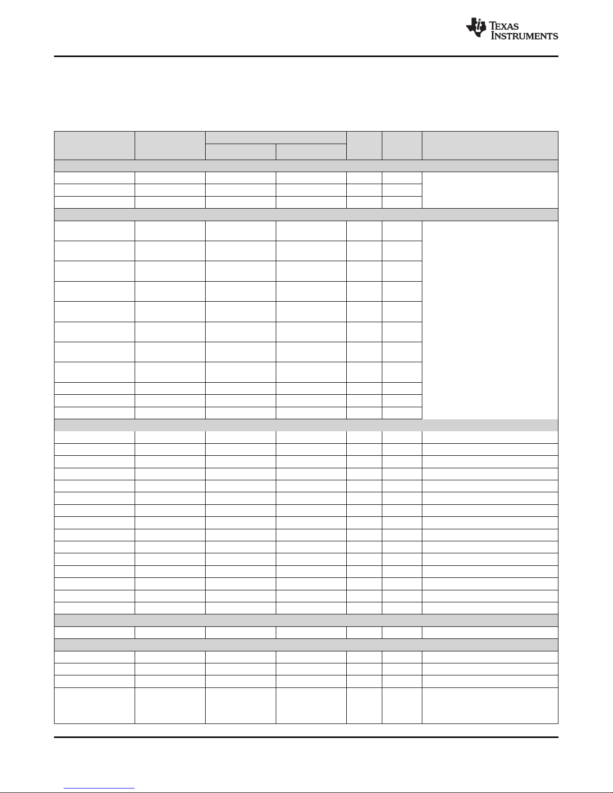
TMS570LS0714
SPNS226E –JUNE 2013–REVISED NOVEMBER 2016
6.9.2 Memory Map Table
See Figure 1-1 for block diagrams showing the devices interconnect.
Table 6-20. Device Memory Map
MODULE NAME
TCM Flash CS0 0x0000_0000 0x00FF_FFFF 16MB 768KB
Mirrored Flash Flash mirror frame 0x2000_0000 0x20FF_FFFF 16MB 768KB
Customer OTP, TCM
Flash Banks
Customer OTP,
Bank 7
Customer OTP–ECC,
TCM Flash Banks
Customer OTP–ECC,
Bank 7
TI OTP, TCM Flash
Banks
TI OTP,
Bank 7
TI OTP–ECC, TCM
Flash Banks
TI OTP–ECC,
Bank 7
Bank 7 – ECC 0xF010_0000 0xF013_FFFF 256KB 8KB
Bank 7 0xF020_0000 0xF03F_FFFF 2MB 64KB
Flash Data Space ECC 0xF040_0000 0xF04F_FFFF 1MB 128KB
ePWM1 0xFCF7_8C00 0xFCF7_8CFF 256B 256B Abort
ePWM2 0xFCF7_8D00 0xFCF7_8DFF 256B 256B Abort
ePWM3 0xFCF7_8E00 0xFCF7_8EFF 256B 256B Abort
ePWM4 0xFCF7_8F00 0xFCF7_8FFF 256B 256B Abort
ePWM5 0xFCF7_9000 0xFCF7_90FF 256B 256B Abort
ePWM6 0xFCF7_9100 0xFCF7_91FF 256B 256B Abort
ePWM7 0xFCF7_9200 0xFCF7_92FF 256B 256B Abort
eCAP1 0xFCF7_9300 0xFCF7_93FF 256B 256B Abort
eCAP2 0xFCF7_9400 0xFCF7_94FF 256B 256B Abort
eCAP3 0xFCF7_9500 0xFCF7_95FF 256B 256B Abort
eCAP4 0xFCF7_9600 0xFCF7_96FF 256B 256B Abort
eCAP5 0xFCF7_9700 0xFCF7_97FF 256B 256B Abort
eCAP6 0xFCF7_9800 0xFCF7_98FF 256B 256B Abort
eQEP1 0xFCF7_9900 0xFCF7_99FF 256B 256B Abort
eQEP2 0xFCF7_9A00 0xFCF7_9AFF 256B 256B Abort
CRC CRC frame 0xFE00_0000 0xFEFF_FFFF 16MB 512B Accesses above 0x200 generate abort.
MIBSPI5 RAM PCS[5] 0xFF0A_0000 0xFF0B_FFFF 128KB 2KB Abort for accesses above 2KB
MIBSPI3 RAM PCS[6] 0xFF0C_0000 0xFF0D_FFFF 128KB 2KB Abort for accesses above 2KB
MIBSPI1 RAM PCS[7] 0xFF0E_0000 0xFF0F_FFFF 128KB 2KB Abort for accesses above 2KB
DCAN3 RAM PCS[13] 0xFF1A_0000 0xFF1B_FFFF 128KB 2KB
FRAME CHIP
SELECT
FRAME ADDRESS RANGE
START END
Memories tightly coupled to the ARM Cortex-R4F CPU
Flash Module Bus2 Interface
0xF000_0000 0xF000_1FFF 8KB 4KB
0xF000_E000 0xF000_FFFF 8KB 1KB
0xF004_0000 0xF004_03FF 1KB 512B
0xF004_1C00 0xF004_1FFF 1KB 128B
0xF008_0000 0xF008_1FFF 8KB 4KB
0xF008_E000 0xF008_FFFF 8KB 1KB
0xF00C_0000 0xF00C_03FF 1KB 512B
0xF00C_1C00 0xF00C_1FFF 1KB 128B
SCR5: Enhanced Timer Peripherals
Cyclic Redundancy Checker (CRC) Module Registers
Peripheral Memories
FRAME
SIZE
ACTUAL
SIZE
RESPONSE FOR ACCESS TO
UNIMPLEMENTED LOCATIONS IN
FRAME
AbortTCM RAM + RAM ECC CSRAM0 0x0800_0000 0x0BFF_FFFF 64MB 96KB
Abort
Wrap around for accesses to
unimplemented address offsets lower
than 0x7FF. Abort generated for
accesses beyond offset 0x800.
www.ti.com
62
System Information and Electrical Specifications Copyright © 2013–2016, Texas Instruments Incorporated
Submit Documentation Feedback
Product Folder Links: TMS570LS0714
Page 63

TMS570LS0714
www.ti.com
SPNS226E –JUNE 2013–REVISED NOVEMBER 2016
Table 6-20. Device Memory Map (continued)
MODULE NAME
DCAN2 RAM PCS[14] 0xFF1C_0000 0xFF1D_FFFF 128KB 2KB
DCAN1 RAM PCS[15] 0xFF1E_0000 0xFF1F_FFFF 128KB 2KB
MIBADC2 RAM
MIBADC2
Look-Up Table
MIBADC1 RAM
MibADC1
Look-Up Table
N2HET2 RAM PCS[34] 0xFF44_0000 0xFF45_FFFF 128KB 16KB
N2HET1 RAM PCS[35] 0xFF46_0000 0xFF47_FFFF 128KB 16KB
N2HET2 TU2 RAM PCS[38] 0xFF4C_0000 0xFF4D_FFFF 128KB 1KB Abort
N2HET1 TU1 RAM PCS[39] 0xFF4E_0000 0xFF4F_FFFF 128KB 1KB Abort
CoreSight Debug ROM CSCS0 0xFFA0_0000 0xFFA0_0FFF 4KB 4KB Reads return zeros, writes have no effect
Cortex-R4F Debug CSCS1 0xFFA0_1000 0xFFA0_1FFF 4KB 4KB Reads return zeros, writes have no effect
HTU1 PS[22] 0xFFF7_A400 0xFFF7_A4FF 256B 256B Reads return zeros, writes have no effect
HTU2 PS[22] 0xFFF7_A500 0xFFF7_A5FF 256B 256B Reads return zeros, writes have no effect
N2HET1 PS[17] 0xFFF7_B800 0xFFF7_B8FF 256B 256B Reads return zeros, writes have no effect
N2HET2 PS[17] 0xFFF7_B900 0xFFF7_B9FF 256B 256B Reads return zeros, writes have no effect
GIO PS[16] 0xFFF7_BC00 0xFFF7_BDFF 512B 256B Reads return zeros, writes have no effect
MIBADC1 PS[15] 0xFFF7_C000 0xFFF7_C1FF 512B 512B Reads return zeros, writes have no effect
MIBADC2 PS[15] 0xFFF7_C200 0xFFF7_C3FF 512B 512B Reads return zeros, writes have no effect
I2C PS[10] 0xFFF7_D400 0xFFF7_D4FF 256B 256B Reads return zeros, writes have no effect
DCAN1 PS[8] 0xFFF7_DC00 0xFFF7_DDFF 512B 512B Reads return zeros, writes have no effect
DCAN2 PS[8] 0xFFF7_DE00 0xFFF7_DFFF 512B 512B Reads return zeros, writes have no effect
DCAN3 PS[7] 0xFFF7_E000 0xFFF7_E1FF 512B 512B Reads return zeros, writes have no effect
LIN PS[6] 0xFFF7_E400 0xFFF7_E4FF 256B 256B Reads return zeros, writes have no effect
SCI PS[6] 0xFFF7_E500 0xFFF7_E5FF 256B 256B Reads return zeros, writes have no effect
MibSPI1 PS[2] 0xFFF7_F400 0xFFF7_F5FF 512B 512B Reads return zeros, writes have no effect
SPI2 PS[2] 0xFFF7_F600 0xFFF7_F7FF 512B 512B Reads return zeros, writes have no effect
MibSPI3 PS[1] 0xFFF7_F800 0xFFF7_F9FF 512B 512B Reads return zeros, writes have no effect
SPI4 PS[1] 0xFFF7_FA00 0xFFF7_FBFF 512B 512B Reads return zeros, writes have no effect
MibSPI5 PS[0] 0xFFF7_FC00 0xFFF7_FDFF 512B 512B Reads return zeros, writes have no effect
FRAME CHIP
SELECT
PCS[29] 0xFF3A_0000 0xFF3B_FFFF 128KB
PCS[31] 0xFF3E_0000 0xFF3F_FFFF 128KB
FRAME ADDRESS RANGE
START END
Debug Components
Peripheral Control Registers
FRAME
SIZE
ACTUAL
SIZE
8KB
384B
8KB
384B
RESPONSE FOR ACCESS TO
UNIMPLEMENTED LOCATIONS IN
FRAME
Wrap around for accesses to
unimplemented address offsets lower
than 0x7FF. Abort generated for
accesses beyond offset 0x800.
Wrap around for accesses to
unimplemented address offsets lower
than 0x7FF. Abort generated for
accesses beyond offset 0x800.
Wrap around for accesses to
unimplemented address offsets lower
than 0x1FFF. Abort generated for
accesses beyond 0x1FFF.
Look-Up Table for ADC2 wrapper. Starts
at address offset 0x2000 and ends at
address offset 0x217F. Wrap around for
accesses between offsets 0x0180 and
0x3FFF. Abort generated for accesses
beyond offset 0x4000.
Wrap around for accesses to
unimplemented address offsets lower
than 0x1FFF. Abort generated for
accesses beyond 0x1FFF.
Look-Up Table for ADC1 wrapper. Starts
at address offset 0x2000 and ends at
address offset 0x217F. Wrap around for
accesses between offsets 0x0180 and
0x3FFF. Abort generated for accesses
beyond offset 0x4000.
Wrap around for accesses to
unimplemented address offsets lower
than 0x3FFF. Abort generated for
accesses beyond 0x3FFF.
Wrap around for accesses to
unimplemented address offsets lower
than 0x3FFF. Abort generated for
accesses beyond 0x3FFF.
System Information and Electrical SpecificationsCopyright © 2013–2016, Texas Instruments Incorporated
Submit Documentation Feedback
Product Folder Links: TMS570LS0714
63
Page 64

TMS570LS0714
SPNS226E –JUNE 2013–REVISED NOVEMBER 2016
www.ti.com
Table 6-20. Device Memory Map (continued)
MODULE NAME
DMA RAM PPCS0 0xFFF8_0000 0xFFF8_0FFF 4KB 4KB Abort
VIM RAM PPCS2 0xFFF8_2000 0xFFF8_2FFF 4KB 1KB
Flash Module PPCS7 0xFFF8_7000 0xFFF8_7FFF 4KB 4KB Abort
eFuse Controller PPCS12 0xFFF8_C000 0xFFF8_CFFF 4KB 4KB Abort
Power Management
Module (PMM)
PCR registers PPS0 0xFFFF_E000 0xFFFF_E0FF 256B 256B Reads return zeros, writes have no effect
System Module -
Frame 2
(see device TRM)
PBIST PPS1 0xFFFF_E400 0xFFFF_E5FF 512B 512B Reads return zeros, writes have no effect
STC PPS1 0xFFFF_E600 0xFFFF_E6FF 256B 256B
IOMM Multiplexing
Control Module
DCC1 PPS3 0xFFFF_EC00 0xFFFF_ECFF 256B 256B Reads return zeros, writes have no effect
DMA PPS4 0xFFFF_F000 0xFFFF_F3FF 1KB 1KB Reads return zeros, writes have no effect
DCC2 PPS5 0xFFFF_F400 0xFFFF_F4FF 256B 256B Reads return zeros, writes have no effect
ESM PPS5 0xFFFF_F500 0xFFFF_F5FF 256B 256B Reads return zeros, writes have no effect
CCMR4 PPS5 0xFFFF_F600 0xFFFF_F6FF 256B 256B Reads return zeros, writes have no effect
RAM ECC even PPS6 0xFFFF_F800 0xFFFF_F8FF 256B 256B Reads return zeros, writes have no effect
RAM ECC odd PPS6 0xFFFF_F900 0xFFFF_F9FF 256B 256B Reads return zeros, writes have no effect
RTI + DWWD PPS7 0xFFFF_FC00 0xFFFF_FCFF 256B 256B Reads return zeros, writes have no effect
VIM Parity PPS7 0xFFFF_FD00 0xFFFF_FDFF 256B 256B Reads return zeros, writes have no effect
VIM PPS7 0xFFFF_FE00 0xFFFF_FEFF 256B 256B Reads return zeros, writes have no effect
System Module -
Frame 1
(see device TRM)
FRAME CHIP
SELECT
PPSE0 0xFFFF_0000 0xFFFF_01FF 512B 512B Abort
PPS0 0xFFFF_E100 0xFFFF_E1FF 256B 256B Reads return zeros, writes have no effect
PPS2 0xFFFF_EA00 0xFFFF_EBFF 512B 512B Reads return zeros, writes have no effect
PPS7 0xFFFF_FF00 0xFFFF_FFFF 256B 256B Reads return zeros, writes have no effect
FRAME ADDRESS RANGE
START END
System Modules Control Registers and Memories
FRAME
SIZE
ACTUAL
SIZE
RESPONSE FOR ACCESS TO
UNIMPLEMENTED LOCATIONS IN
FRAME
Wrap around for accesses to
unimplemented address offsets between
1KB and 4KB.
Generates address error interrupt, if
enabled
6.9.3 Special Consideration for CPU Access Errors Resulting in Imprecise Aborts
Any CPU write access to a Normal or Device type memory, which generates a fault, will generate an
imprecise abort. The imprecise abort exception is disabled by default and must be enabled for the CPU to
handle this exception. The imprecise abort handling is enabled by clearing the "A" bit in the CPU program
status register (CPSR).
64
System Information and Electrical Specifications Copyright © 2013–2016, Texas Instruments Incorporated
Submit Documentation Feedback
Product Folder Links: TMS570LS0714
Page 65

TMS570LS0714
www.ti.com
SPNS226E –JUNE 2013–REVISED NOVEMBER 2016
6.9.4 Master/Slave Access Privileges
Table 6-21 lists the access permissions for each bus master on the device. A bus master is a module that
can initiate a read or a write transaction on the device.
Each slave module on the main interconnect is listed in the table. Yes indicates that the module listed in
the MASTERS column can access that slave module.
Table 6-21. Master / Slave Access Matrix
MASTERS ACCESS MODE SLAVES ON MAIN SCR
Flash Module
Bus2 Interface:
OTP, ECC, Bank
7
CPU READ User/Privilege Yes Yes Yes Yes Yes
CPU WRITE User/Privilege No Yes Yes Yes Yes
DMA User Yes Yes Yes Yes Yes
DAP Privilege Yes Yes Yes Yes Yes
HTU1 Privilege No Yes Yes Yes Yes
HTU2 Privilege No Yes Yes Yes Yes
Non-CPU
Accesses to
Program Flash
and CPU Data
RAM
CRC Slave Interfaces Peripheral
Memories, And
Module Control
Control
Registers, All
Peripheral
All System
Registers And
Memories
6.9.5 Special Notes on Accesses to Certain Slaves
Write accesses to the Power Domain Management Module (PMM) control registers are limited to the CPU
(master id = 1). The other masters can only read from these registers.
A debugger can also write to the PMM registers. The master-id check is disabled in debug mode.
The device contains dedicated logic to generate a bus error response on any access to a module that is in
a power domain that has been turned off.
System Information and Electrical SpecificationsCopyright © 2013–2016, Texas Instruments Incorporated
Submit Documentation Feedback
Product Folder Links: TMS570LS0714
65
Page 66
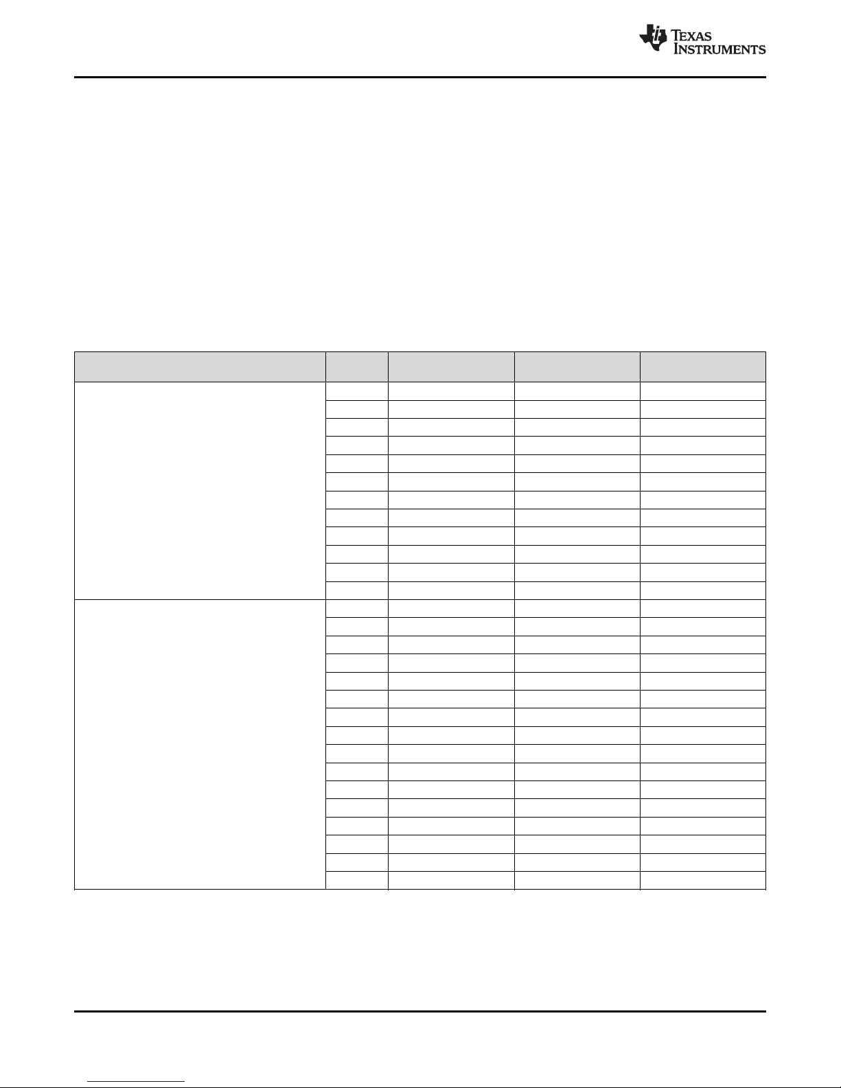
TMS570LS0714
SPNS226E –JUNE 2013–REVISED NOVEMBER 2016
6.10 Flash Memory
6.10.1 Flash Memory Configuration
Flash Bank: A separate block of logic consisting of 1 to 16 sectors. Each flash bank normally has a
customer-OTP and a TI-OTP area. These flash sectors share input/output buffers, data paths, sense
amplifiers, and control logic.
Flash Sector: A contiguous region of flash memory which must be erased simultaneously due to physical
construction constraints.
Flash Pump: A charge pump which generates all the voltages required for reading, programming, or
erasing the flash banks.
Flash Module: Interface circuitry required between the host CPU and the flash banks and pump module.
Table 6-22. Flash Memory Banks and Sectors
www.ti.com
MEMORY ARRAYS (OR BANKS)
BANK0 (768KB)
BANK7 (64KB) for EEPROM emulation
(1) Flash bank0 is a 144-bit-wide bank with ECC support.
(2) Flash bank7 is a 72-bit-wide bank with ECC support.
(3) The flash bank7 can be programmed while executing code from flash bank0.
(4) Code execution is not allowed from flash bank7.
(1)
(2)(3)(4)
SECTOR
NO.
0 16KB 0x0000_0000 0x0000_3FFF
1 16KB 0x0000_4000 0x0000_7FFF
2 16KB 0x0000_8000 0x0000_BFFF
3 16KB 0x0000_C000 0x0000_FFFF
4 16KB 0x0001_0000 0x0001_3FFF
5 16KB 0x0001_4000 0x0001_7FFF
6 32KB 0x0001_8000 0x0001_FFFF
7 128KB 0x0002_0000 0x0003_FFFF
8 128KB 0x0004_0000 0x0005_FFFF
9 128KB 0x0006_0000 0x0007_FFFF
10 128KB 0x0008_0000 0x0009_FFFF
11 128KB 0x000A_0000 0x000B_FFFF
0 4KB 0xF020_0000 0xF020_0FFF
1 4KB 0xF020_1000 0xF020_1FFF
2 4KB 0xF020_2000 0xF020_2FFF
3 4KB 0xF020_3000 0xF020_3FFF
4 4KB 0xF020_4000 0xF020_4FFF
5 4KB 0xF020_5000 0xF020_5FFF
6 4KB 0xF020_6000 0xF020_6FFF
7 4KB 0xF020_7000 0xF020_7FFF
8 4KB 0xF020_8000 0xF020_8FFF
9 4KB 0xF020_9000 0xF020_9FFF
10 4KB 0xF020_A000 0xF020_AFFF
11 4KB 0xF020_B000 0xF020_BFFF
12 4KB 0xF020_C000 0xF020_CFFF
13 4KB 0xF020_D000 0xF020_DFFF
14 4KB 0xF020_E000 0xF020_EFFF
15 4KB 0xF020_F000 0xF020_FFFF
SEGMENT LOW ADDRESS HIGH ADDRESS
66
System Information and Electrical Specifications Copyright © 2013–2016, Texas Instruments Incorporated
Submit Documentation Feedback
Product Folder Links: TMS570LS0714
Page 67

www.ti.com
6.10.2 Main Features of Flash Module
• Support for multiple flash banks for program and/or data storage
• Simultaneous read access on a bank while performing program or erase operation on any other bank
• Integrated state machines to automate flash erase and program operations
• Pipelined mode operation to improve instruction access interface bandwidth
• Support for Single Error Correction Double Error Detection (SECDED) block inside Cortex-R4F CPU
– Error address is captured for host system debugging
• Support for a rich set of diagnostic features
6.10.3 ECC Protection for Flash Accesses
All accesses to the program flash memory are protected by SECDED logic embedded inside the CPU.
The flash module provides 8 bits of ECC code for 64 bits of instructions or data fetched from the flash
memory. The CPU calculates the expected ECC code based on the 64 bits received and compares it with
the ECC code returned by the flash module. A single-bit error is corrected and flagged by the CPU, while
a multibit error is only flagged. The CPU signals an ECC error through its Event bus. This signaling
mechanism is not enabled by default and must be enabled by setting the "X" bit of the Performance
Monitor Control Register, c9.
MRC p15,#0,r1,c9,c12,#0 ;Enabling Event monitor states
ORR r1, r1, #0x00000010
MCR p15,#0,r1,c9,c12,#0 ;Set 4th bit (‘X’) of PMNC register
MRC p15,#0,r1,c9,c12,#0
TMS570LS0714
SPNS226E –JUNE 2013–REVISED NOVEMBER 2016
The application must also explicitly enable the ECC checking of the CPU for accesses on the CPU ATCM
and BTCM interfaces. These are connected to the program flash and data RAM, respectively. ECC
checking for these interfaces can be done by setting the B1TCMPCEN, B0TCMPCEN, and ATCMPCEN
bits of the System Control Coprocessor Auxiliary Control Register, c1.
MRC p15, #0, r1, c1, c0, #1
ORR r1, r1, #0x0e000000 ;Enable ECC checking for ATCM and BTCMs
DMB
MCR p15, #0, r1, c1, c0, #1
6.10.4 Flash Access Speeds
For information on flash memory access speeds and the relevant wait states required, see
Section 5.8.1.2.
System Information and Electrical SpecificationsCopyright © 2013–2016, Texas Instruments Incorporated
Submit Documentation Feedback
Product Folder Links: TMS570LS0714
67
Page 68

TMS570LS0714
SPNS226E –JUNE 2013–REVISED NOVEMBER 2016
www.ti.com
6.10.5 Program Flash
Table 6-23. Timing Requirements for Program Flash
MIN NOM MAX UNIT
t
prog(144bit)
t
prog(Total)
t
erase(bank0)
t
wec
(1) This programming time includes overhead of state machine, but does not include data transfer time. The programming time assumes
programming 144 bits at a time at the maximum specified operating frequency.
(2) During bank erase, the selected sectors are erased simultaneously. The time to erase the bank is specified as equal to the time to erase
a sector.
Wide Word (144-bit) programming time 40 300 µs
768KB programming time
Sector/Bank erase time
(1)
(2)
Write/erase cycles with 15-year Data Retention
requirement
–40°C to 125°C 8 s
0°C to 60°C, for first
25 cycles
2 4 s
–40°C to 125°C 0.03 4 s
0°C to 60°C, for first
25 cycles
16 100 ms
–40°C to 125°C 1000 cycles
6.10.6 Data Flash
Table 6-24. Timing Requirements for Data Flash
MIN NOM MAX UNIT
t
prog(144bit)
t
prog(Total)
t
erase(bank7)
t
wec
Wide Word (72-bit) programming time 47 310 µs
EEPROM Emulation (bank 7) 64KByte
programming time
(1)
Sector/Bank erase time, EEPROM Emulation
(bank 7)
Write/erase cycles with 15-year Data Retention
requirement
–40°C to 125°C 2.6 s
0°C to 60°C, for first
25 cycles
775 1435 ms
–40°C to 125°C 0.2 8 s
0°C to 60°C, for first
25 cycles
14 100 ms
–40°C to 125°C 100000 cycles
(1) This programming time includes overhead of state machine, but does not include data transfer time. The programming time assumes
programming 72 bits at a time at the maximum specified operating frequency.
68
System Information and Electrical Specifications Copyright © 2013–2016, Texas Instruments Incorporated
Submit Documentation Feedback
Product Folder Links: TMS570LS0714
Page 69

TCM BUS
TCM BUS
72-bit data + ECC
72-bit data + ECC
Upper 32-bits data
and 4 ECC bits
Lower 32-bits data
and 4 ECC bits
36 Bit
wide
RAM
36 Bit
36-bit-wide
RAM
36 Bit
wide
RAM
36 Bit
RAM
Upper 32-bits data
and 4 ECC bits
Lower 32-bits data
and 4 ECC bits
36 Bit
wide
RAM
36 Bit
36 Bit
wide
RAM
36 Bit
wide
RAM
TCRAM
Interface 1
Cortex R4)Œ
B0
TCM
B1
TCM
TCRAM
Interface 2
36-bit-wide
RAM
36-bit-wide
RAM
36-bit-wide
RAM
www.ti.com
6.11 Tightly Coupled RAM Interface Module
Figure 6-10 shows the connection of the Tightly Coupled RAM (TCRAM) to the Cortex-R4F™ CPU.
TMS570LS0714
SPNS226E –JUNE 2013–REVISED NOVEMBER 2016
6.11.1 Features
The features of the Tightly Coupled RAM (TCRAM) Module are:
• Acts as slave to the BTCM interface of the Cortex-R4F CPU
• Supports CPU internal ECC scheme by providing 64-bit data and 8-bit ECC code
• Monitors CPU Event Bus and generates single-bit or multibit error interrupts
• Stores addresses for single-bit and multibit errors
• Supports RAM trace module
• Provides CPU address bus integrity checking by supporting parity checking on the address bus
• Performs redundant address decoding for the RAM bank chip select and ECC select generation logic
• Provides enhanced safety for the RAM addressing by implementing two 36-bit-wide byte-interleaved RAM banks
and generating independent RAM access control signals to the two banks
• Supports auto-initialization of the RAM banks along with the ECC bits
6.11.2 TCRAMW ECC Support
The TCRAMW passes on the ECC code for each data read by the Cortex-R4F CPU from the RAM. The
TCRAMW also stores the ECC port contents of the CPU in the ECC RAM when the CPU does a write to
the RAM. The TCRAMW monitors the CPU event bus and provides registers for indicating single-bit or
multibit errors and also for identifying the address that caused the single or multi-bit error. The event
signaling and the ECC checking for the RAM accesses must be enabled inside the CPU.
For more information, see the device-specific Technical Reference Manual.
6.12 Parity Protection for Accesses to Peripheral RAMs
Accesses to some peripheral RAMs are protected by odd/even parity checking. During a read access the
parity is calculated based on the data read from the peripheral RAM and compared with the good parity
value stored in the parity RAM for that peripheral. If any word fails the parity check, the module generates
a parity error signal that is mapped to the Error Signaling Module. The module also captures the
peripheral RAM address that caused the parity error.
Figure 6-10. TCRAM Block Diagram
Submit Documentation Feedback
Product Folder Links: TMS570LS0714
System Information and Electrical SpecificationsCopyright © 2013–2016, Texas Instruments Incorporated
69
Page 70

TMS570LS0714
SPNS226E –JUNE 2013–REVISED NOVEMBER 2016
The parity protection for peripheral RAMs is not enabled by default and must be enabled by the
application. Each individual peripheral contains control registers to enable the parity protection for
accesses to its RAM.
The CPU read access gets the actual data from the peripheral. The application can choose
to generate an interrupt whenever a peripheral RAM parity error is detected.
www.ti.com
NOTE
70
System Information and Electrical Specifications Copyright © 2013–2016, Texas Instruments Incorporated
Submit Documentation Feedback
Product Folder Links: TMS570LS0714
Page 71

TMS570LS0714
www.ti.com
SPNS226E –JUNE 2013–REVISED NOVEMBER 2016
6.13 On-Chip SRAM Initialization and Testing
6.13.1 On-Chip SRAM Self-Test Using PBIST
6.13.1.1 Features
• Extensive instruction set to support various memory test algorithms
• ROM-based algorithms allow application to run TI production-level memory tests
• Independent testing of all on-chip SRAM
6.13.1.2 PBIST RAM Groups
Table 6-25. PBIST RAM Grouping
Test Pattern (Algorithm)
0x4
(1)
MARCH 13N
SINGLE PORT
(cycles)
ALGO MASK
0x8
MEMORY
PBIST_ROM 1 ROM CLK ROM 24578 8194
STC_ROM 2 ROM CLK ROM 19586 6530
DCAN1 3 VCLK Dual port 25200
DCAN2 4 VCLK Dual port 25200
DCAN3 5 VCLK Dual port 25200
ESRAM1
MIBADC1 11 VCLK Dual port 4200
HET TU1 14 VCLK Dual port 6480
MIBADC2 18 VCLK Dual port 4200
HET TU2 20 VCLK Dual port 6480
ESRAM5
(1) Several memory testing algorithms are stored in the PBIST ROM. However, TI recommends the March13N algorithm for application
testing of RAM.
(2) ESRAM1: Address 0x08000000 - 0x0800FFFF
(3) ESRAM5: Address 0x08010000 - 0x0801FFFF
(2)
MIBSPI1 7 VCLK Dual port 33440
MIBSPI3 8 VCLK Dual port 33440
MIBSPI5 9 VCLK Dual port 33440
VIM 10 VCLK Dual port 12560
DMA 12 HCLK Dual port 18960
N2HET1 13 VCLK Dual port 31680
N2HET2 19 VCLK Dual port 31680
(3)
RAM
GROUP
6 HCLK Single port 266280
21 HCLK Single port 266280
TEST CLOCK
MEM
TYPE
TRIPLE READ
SLOW READ
ALGO MASK
0x1
TRIPLE READ
FAST READ
ALGO MASK
0x2
MARCH 13N
TWO PORT
(cycles)
ALGO MASK
(1)
The PBIST ROM clock frequency is limited to 100 MHz, if 100 MHz < HCLK <= HCLKmax, or HCLK, if
HCLK <= 100 MHz.
The PBIST ROM clock is divided down from HCLK. The divider is selected by programming the ROM_DIV
field of the Memory Self-Test Global Control Register (MSTGCR) at address 0xFFFFFF58.
System Information and Electrical SpecificationsCopyright © 2013–2016, Texas Instruments Incorporated
Submit Documentation Feedback
Product Folder Links: TMS570LS0714
71
Page 72

TMS570LS0714
SPNS226E –JUNE 2013–REVISED NOVEMBER 2016
6.13.2 On-Chip SRAM Auto Initialization
This microcontroller allows some of the on-chip memories to be initialized through the Memory Hardware
Initialization mechanism in the system module. This hardware mechanism allows an application to
program the memory arrays with error detection capability to a known state based on their error detection
scheme (odd/even parity or ECC).
The MINITGCR register enables the memory initialization sequence, and the MSINENA register selects
the memories that are to be initialized.
For more information on these registers, see the device-specific Technical Reference Manual.
The mapping of the different on-chip memories to the specific bits of the MSINENA registers is shown in
Table 6-26.
Table 6-26. Memory Initialization
www.ti.com
CONNECTING MODULE
RAM (PD#1) 0x08000000 0x0800FFFF 0
RAM (RAM_PD#1) 0x08010000 0x0801FFFF 0
MIBSPI5 RAM 0xFF0A0000 0xFF0BFFFF 12
MIBSPI3 RAM 0xFF0C0000 0xFF0DFFFF 11
MIBSPI1 RAM 0xFF0E0000 0xFF0FFFFF 7
DCAN3 RAM 0xFF1A0000 0xFF1BFFFF 10
DCAN2 RAM 0xFF1C0000 0xFF1DFFFF 6
DCAN1 RAM 0xFF1E0000 0xFF1FFFFF 5
MIBADC2 RAM 0xFF3A0000 0xFF3BFFFF 14
MIBADC1 RAM 0xFF3E0000 0xFF3FFFFF 8
N2HET2 RAM 0xFF440000 0xFF45FFFF 15
N2HET1 RAM 0xFF460000 0xFF47FFFF 3
HET TU2 RAM 0xFF4C0000 0xFF4DFFFF 16
HET TU1 RAM 0xFF4E0000 0xFF4FFFFF 4
DMA RAM 0xFFF80000 0xFFF80FFF 1
VIM RAM 0xFFF82000 0xFFF82FFF 2
(1) The TCM RAM wrapper has separate control bits to select the RAM power domain that is to be auto-initialized.
(2) The MibSPIx modules perform an initialization of the transmit and receive RAMs as soon as the module is released from its local reset.
This is independent of whether the application chooses to initialize the MibSPIx RAMs using the system module auto-initialization
method. The MibSPIx module must be first brought out of its local reset to use the system module auto-initialization method.
BASE ADDRESS ENDING ADDRESS
ADDRESS RANGE
MSINENA REGISTER BIT #
(1)
(1)
(2)
(2)
(2)
72
System Information and Electrical Specifications Copyright © 2013–2016, Texas Instruments Incorporated
Submit Documentation Feedback
Product Folder Links: TMS570LS0714
Page 73

www.ti.com
6.14 Vectored Interrupt Manager
The vectored interrupt manager (VIM) provides hardware assistance for prioritizing and controlling the
many interrupt sources present on this device. Interrupts are caused by events outside of the normal flow
of program execution. Normally, these events require a timely response from the CPU; therefore, when an
interrupt occurs, the CPU switches execution from the normal program flow to an interrupt service routine
(ISR).
6.14.1 VIM Features
The VIM module has the following features:
• Supports 128 interrupt channels.
– Provides programmable priority and enable for interrupt request lines.
• Provides a direct hardware dispatch mechanism for fastest IRQ dispatch.
• Provides two software dispatch mechanisms when the CPU VIC port is not used.
– Index interrupt
– Register vectored interrupt
• Parity protected vector interrupt table against soft errors.
6.14.2 Interrupt Request Assignments
TMS570LS0714
SPNS226E –JUNE 2013–REVISED NOVEMBER 2016
Table 6-27. Interrupt Request Assignments
Modules Interrupt Sources Default VIM Interrupt
ESM ESM High level interrupt (NMI) 0
Reserved Reserved 1
RTI RTI compare interrupt 0 2
RTI RTI compare interrupt 1 3
RTI RTI compare interrupt 2 4
RTI RTI compare interrupt 3 5
RTI RTI overflow interrupt 0 6
RTI RTI overflow interrupt 1 7
RTI RTI time-base interrupt 8
GIO GIO interrupt A 9
N2HET1 N2HET1 level 0 interrupt 10
HET TU1 HET TU1 level 0 interrupt 11
MIBSPI1 MIBSPI1 level 0 interrupt 12
LIN LIN level 0 interrupt 13
MIBADC1 MIBADC1 event group interrupt 14
MIBADC1 MIBADC1 software group 1 interrupt 15
DCAN1 DCAN1 level 0 interrupt 16
SPI2 SPI2 level 0 interrupt 17
Reserved Reserved 18
CRC CRC Interrupt 19
ESM ESM low-level interrupt 20
SYSTEM Software interrupt (SSI) 21
CPU PMU Interrupt 22
GIO GIO interrupt B 23
N2HET1 N2HET1 level 1 interrupt 24
HET TU1 HET TU1 level 1 interrupt 25
MIBSPI1 MIBSPI1 level 1 interrupt 26
Channel
System Information and Electrical SpecificationsCopyright © 2013–2016, Texas Instruments Incorporated
Submit Documentation Feedback
Product Folder Links: TMS570LS0714
73
Page 74

TMS570LS0714
SPNS226E –JUNE 2013–REVISED NOVEMBER 2016
Table 6-27. Interrupt Request Assignments (continued)
Modules Interrupt Sources Default VIM Interrupt
LIN LIN level 1 interrupt 27
MIBADC1 MIBADC1 software group 2 interrupt 28
DCAN1 DCAN1 level 1 interrupt 29
SPI2 SPI2 level 1 interrupt 30
MIBADC1 MIBADC1 magnitude compare interrupt 31
Reserved Reserved 32
DMA FTCA interrupt 33
DMA LFSA interrupt 34
DCAN2 DCAN2 level 0 interrupt 35
MIBSPI3 MIBSPI3 level 0 interrupt 37
MIBSPI3 MIBSPI3 level 1 interrupt 38
DMA HBCA interrupt 39
DMA BTCA interrupt 40
Reserved Reserved 41
DCAN2 DCAN2 level 1 interrupt 42
DCAN1 DCAN1 IF3 interrupt 44
DCAN3 DCAN3 level 0 interrupt 45
DCAN2 DCAN2 IF3 interrupt 46
FPU FPU interrupt 47
Reserved Reserved 48
SPI4 SPI4 level 0 interrupt 49
MIBADC2 MibADC2 event group interrupt 50
MIBADC2 MibADC2 software group1 interrupt 51
Reserved Reserved 52
MIBSPI5 MIBSPI5 level 0 interrupt 53
SPI4 SPI4 level 1 interrupt 54
DCAN3 DCAN3 level 1 interrupt 55
MIBSPI5 MIBSPI5 level 1 interrupt 56
MIBADC2 MibADC2 software group2 interrupt 57
Reserved Reserved 58
MIBADC2 MibADC2 magnitude compare interrupt 59
DCAN3 DCAN3 IF3 interrupt 60
FMC FSM_DONE interrupt 61
Reserved Reserved 62
N2HET2 N2HET2 level 0 interrupt 63
SCI SCI level 0 interrupt 64
HET TU2 HET TU2 level 0 interrupt 65
I2C I2C level 0 interrupt 66
Reserved Reserved 67–72
N2HET2 N2HET2 level 1 interrupt 73
SCI SCI level 1 interrupt 74
HET TU2 HET TU2 level 1 interrupt 75
Reserved Reserved 76–79
HWAG1 HWA_INT_REQ_H 80
HWAG2 HWA_INT_REQ_H 81
DCC1 DCC done interrupt 82
DCC2 DCC2 done interrupt 83
www.ti.com
Channel
74
System Information and Electrical Specifications Copyright © 2013–2016, Texas Instruments Incorporated
Submit Documentation Feedback
Product Folder Links: TMS570LS0714
Page 75
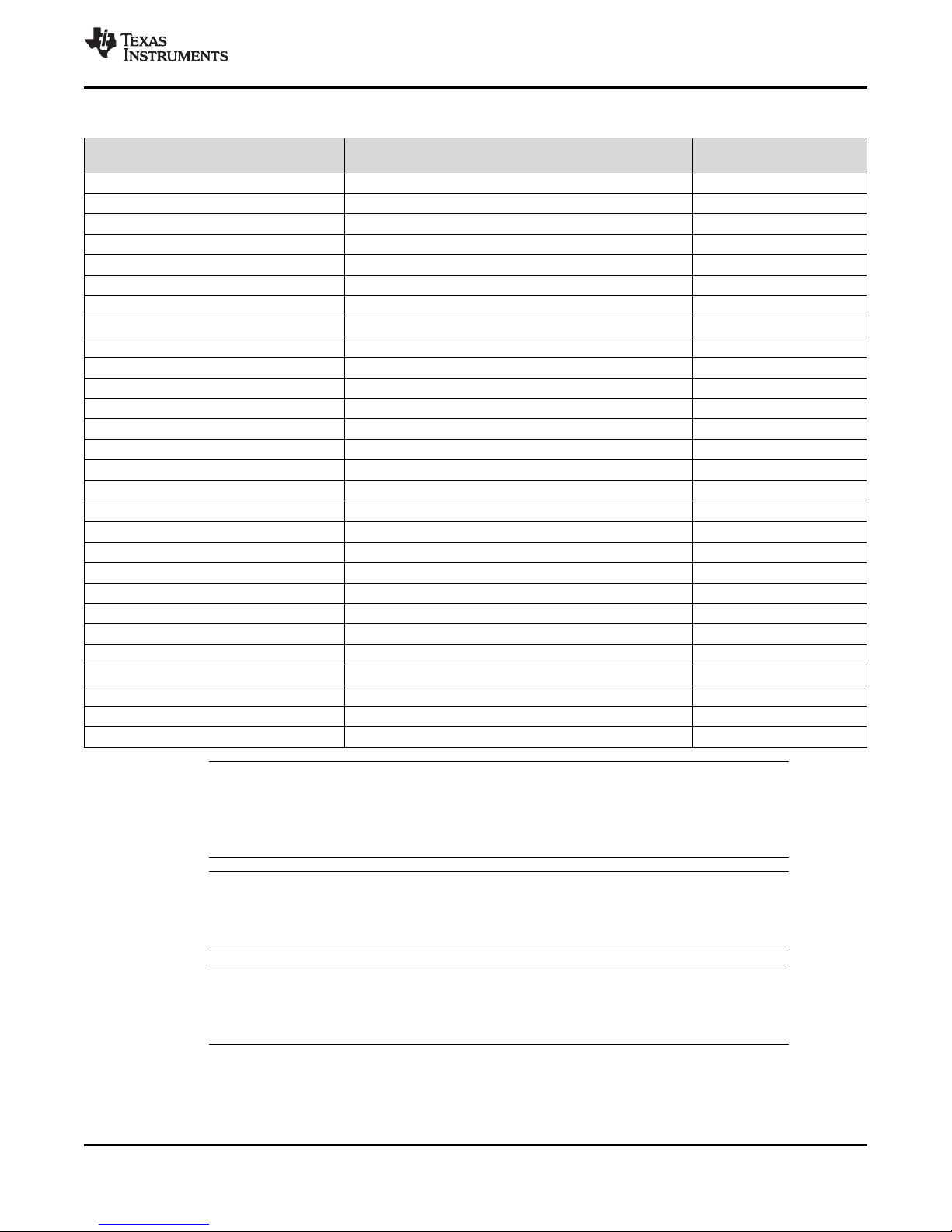
www.ti.com
TMS570LS0714
SPNS226E –JUNE 2013–REVISED NOVEMBER 2016
Table 6-27. Interrupt Request Assignments (continued)
Modules Interrupt Sources Default VIM Interrupt
Channel
Reserved Reserved 84
PBIST Controller PBIST Done Interrupt 85
Reserved Reserved 86-87
HWAG1 HWA_INT_REQ_L 88
HWAG2 HWA_INT_REQ_L 89
ePWM1INTn ePWM1 Interrupt 90
ePWM1TZINTn ePWM1 Trip Zone Interrupt 91
ePWM2INTn ePWM2 Interrupt 92
ePWM2TZINTn ePWM2 Trip Zone Interrupt 93
ePWM3INTn ePWM3 Interrupt 94
ePWM3TZINTn ePWM3 Trip Zone Interrupt 95
ePWM4INTn ePWM4 Interrupt 96
ePWM4TZINTn ePWM4 Trip Zone Interrupt 97
ePWM5INTn ePWM5 Interrupt 98
ePWM5TZINTn ePWM5 Trip Zone Interrupt 99
ePWM6INTn ePWM6 Interrupt 100
ePWM6TZINTn ePWM6 Trip Zone Interrupt 101
ePWM7INTn ePWM7 Interrupt 102
ePWM7TZINTn ePWM7 Trip Zone Interrupt 103
eCAP1INTn eCAP1 Interrupt 104
eCAP2INTn eCAP2 Interrupt 105
eCAP3INTn eCAP3 Interrupt 106
eCAP4INTn eCAP4 Interrupt 107
eCAP5INTn eCAP5 Interrupt 108
eCAP6INTn eCAP6 Interrupt 109
eQEP1INTn eQEP1 Interrupt 110
eQEP2INTn eQEP2 Interrupt 111
Reserved Reserved 112–127
Address location 0x00000000 in the VIM RAM is reserved for the phantom interrupt ISR
entry; therefore only request channels 0..126 can be used and are offset by one address in
the VIM RAM.
The lower-order interrupt channels are higher priority channels than the higher-order interrupt
channels.
The application can change the mapping of interrupt sources to the interrupt channels
through the interrupt channel control registers (CHANCTRLx) inside the VIM module.
NOTE
NOTE
NOTE
System Information and Electrical SpecificationsCopyright © 2013–2016, Texas Instruments Incorporated
Submit Documentation Feedback
Product Folder Links: TMS570LS0714
75
Page 76

TMS570LS0714
SPNS226E –JUNE 2013–REVISED NOVEMBER 2016
6.15 DMA Controller
The DMA controller is used to transfer data between two locations in the memory map in the background
of CPU operations. Typically, the DMA is used to:
• Transfer blocks of data between external and internal data memories
• Restructure portions of internal data memory
• Continually service a peripheral
6.15.1 DMA Features
• CPU independent data transfer
• One 64-bit master port that interfaces to the TMS570 Memory System.
• FIFO buffer (four entries deep and each 64 bits wide)
• Channel control information is stored in RAM protected by parity
• 16 channels with individual enable
• Channel chaining capability
• 32 peripheral DMA requests
• Hardware and software DMA requests
• 8-, 16-, 32- or 64-bit transactions supported
• Multiple addressing modes for source/destination (fixed, increment, offset)
• Auto-initiation
• Power-management mode
• Memory Protection with four configurable memory regions
www.ti.com
76
System Information and Electrical Specifications Copyright © 2013–2016, Texas Instruments Incorporated
Submit Documentation Feedback
Product Folder Links: TMS570LS0714
Page 77

www.ti.com
SPNS226E –JUNE 2013–REVISED NOVEMBER 2016
6.15.2 Default DMA Request Map
The DMA module on this microcontroller has 16 channels and up to 32 hardware DMA requests. The
module contains DREQASIx registers which are used to map the DMA requests to the DMA channels. By
default, channel 0 is mapped to request 0, channel 1 to request 1, and so on.
Some DMA requests have multiple sources, as shown in Table 6-28. The application must ensure that
only one of these DMA request sources is enabled at any time.
Table 6-28. DMA Request Line Connection
Modules DMA Request Sources DMA Request
MIBSPI1 MIBSPI1[1]
MIBSPI1 MIBSPI1[0]
SPI2 SPI2 receive DMAREQ[2]
SPI2 SPI2 transmit DMAREQ[3]
MIBSPI1 / MIBSPI3 / DCAN2 MIBSPI1[2] / MIBSPI3[2] / DCAN2 IF3 DMAREQ[4]
MIBSPI1 / MIBSPI3 / DCAN2 MIBSPI1[3] / MIBSPI3[3] / DCAN2 IF2 DMAREQ[5]
DCAN1 / MIBSPI5 DCAN1 IF2 / MIBSPI5[2] DMAREQ[6]
MIBADC1 / MIBSPI5 MIBADC1 event / MIBSPI5[3] DMAREQ[7]
MIBSPI1 / MIBSPI3 / DCAN1 MIBSPI1[4] / MIBSPI3[4] / DCAN1 IF1 DMAREQ[8]
MIBSPI1 / MIBSPI3 / DCAN2 MIBSPI1[5] / MIBSPI3[5] / DCAN2 IF1 DMAREQ[9]
MIBADC1 / I2C / MIBSPI5 MIBADC1 G1 / I2C receive / MIBSPI5[4] DMAREQ[10]
MIBADC1 / I2C / MIBSPI5 MIBADC1 G2 / I2C transmit / MIBSPI5[5] DMAREQ[11]
RTI / MIBSPI1 / MIBSPI3 RTI DMAREQ0 / MIBSPI1[6] / MIBSPI3[6] DMAREQ[12]
RTI / MIBSPI1 / MIBSPI3 RTI DMAREQ1 / MIBSPI1[7] / MIBSPI3[7] DMAREQ[13]
MIBSPI3 / MibADC2 / MIBSPI5 MIBSPI3[1]
MIBSPI3 / MIBSPI5 MIBSPI3[0]
MIBSPI1 / MIBSPI3 / DCAN1 / MibADC2 MIBSPI1[8] / MIBSPI3[8] / DCAN1 IF3 / MibADC2 G1 DMAREQ[16]
MIBSPI1 / MIBSPI3 / DCAN3 / MibADC2 MIBSPI1[9] / MIBSPI3[9] / DCAN3 IF1 / MibADC2 G2 DMAREQ[17]
RTI / MIBSPI5 RTI DMAREQ2 / MIBSPI5[8] DMAREQ[18]
RTI / MIBSPI5 RTI DMAREQ3 / MIBSPI5[9] DMAREQ[19]
N2HET1 / N2HET2 / DCAN3 N2HET1 DMAREQ[4] / N2HET2 DMAREQ[4] / DCAN3
N2HET1 / N2HET2 / DCAN3 N2HET1 DMAREQ[5] / N2HET2 DMAREQ[5] / DCAN3
MIBSPI1 / MIBSPI3 / MIBSPI5 MIBSPI1[10] / MIBSPI3[10] / MIBSPI5[10] DMAREQ[22]
MIBSPI1 / MIBSPI3 / MIBSPI5 MIBSPI1[11] / MIBSPI3[11] / MIBSPI5[11] DMAREQ[23]
N2HET1 / N2HET2 / SPI4 / MIBSPI5 N2HET1 DMAREQ[6] / N2HET2 DMAREQ[6] / SPI4
N2HET1 / N2HET2 / SPI4 / MIBSPI5 N2HET1 DMAREQ[7] / N2HET2 DMAREQ[7] / SPI4
CRC / MIBSPI1 / MIBSPI3 CRC DMAREQ[0] / MIBSPI1[12] / MIBSPI3[12] DMAREQ[26]
CRC / MIBSPI1 / MIBSPI3 CRC DMAREQ[1] / MIBSPI1[13] / MIBSPI3[13] DMAREQ[27]
LIN / MIBSPI5 LIN receive / MIBSPI5[14] DMAREQ[28]
LIN / MIBSPI5 LIN transmit / MIBSPI5[15] DMAREQ[29]
MIBSPI1 / MIBSPI3 / SCI / MIBSPI5 MIBSPI1[14] / MIBSPI3[14] / SCI receive /
MIBSPI1 / MIBSPI3 / SCI / MIBSPI5 MIBSPI1[15] / MIBSPI3[15] / SCI transmit /
(1) SPI1, SPI3, SPI5 receive when configured in standard SPI mode
(2) SPI1, SPI3, SPI5 transmit when configured in standard SPI mode
(1)
/ MibADC2 event / MIBSPI5[6] DMAREQ[14]
receive / MIBSPI5[12]
transmit / MIBSPI5[13]
MIBSPI5[1]
MIBSPI5[0]
(1)
(2)
(2)
/ MIBSPI5[7] DMAREQ[15]
IF2
IF3
(1)
(2)
TMS570LS0714
DMAREQ[0]
DMAREQ[1]
DMAREQ[20]
DMAREQ[21]
DMAREQ[24]
DMAREQ[25]
DMAREQ[30]
DMAREQ[31]
System Information and Electrical SpecificationsCopyright © 2013–2016, Texas Instruments Incorporated
Submit Documentation Feedback
Product Folder Links: TMS570LS0714
77
Page 78
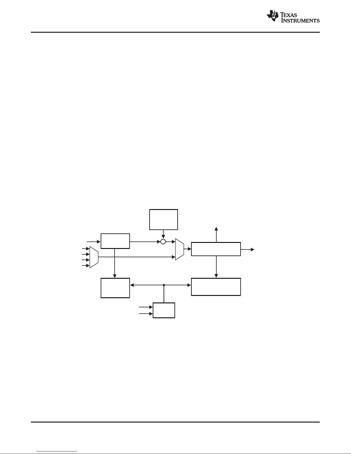
31 0
31 0
31 0
31 0
31 0
External
control
CAP event source 0
CAP event source 1
=
Up counter
Capture
up counter
Compare
up counter
Free-running counter
Capture
RTIFRCx
free-running counter
RTICAFRCx
OVLINTx
RTICPUCx
RTIUCx
RTICAUCx
To Compare
Unit
TMS570LS0714
SPNS226E –JUNE 2013–REVISED NOVEMBER 2016
6.16 Real-Time Interrupt Module
The real-time interrupt (RTI) module provides timer functionality for operating systems and for
benchmarking code. The RTI module can incorporate several counters that define the time bases needed
for scheduling an operating system.
The timers also let you benchmark certain areas of code by reading the values of the counters at the
beginning and the end of the desired code range and calculating the difference between the values.
6.16.1 Features
The RTI module has the following features:
• Two independent 64-bit counter blocks
• Four configurable compares for generating operating system ticks or DMA requests. Each event can
be driven by either counter block 0 or counter block 1.
• Fast enabling/disabling of events
• Two timestamp (capture) functions for system or peripheral interrupts, one for each counter block
6.16.2 Block Diagrams
Figure 6-11 shows a high-level block diagram for one of the two 64-bit counter blocks inside the RTI
module. Both the counter blocks are identical except the Network Time Unit (NTUx) inputs are only
available as time-base inputs for the counter block 0. Figure 6-12 shows the compare unit block diagram
of the RTI module.
www.ti.com
78
System Information and Electrical Specifications Copyright © 2013–2016, Texas Instruments Incorporated
Figure 6-11. Counter Block Diagram
Submit Documentation Feedback
Product Folder Links: TMS570LS0714
Page 79
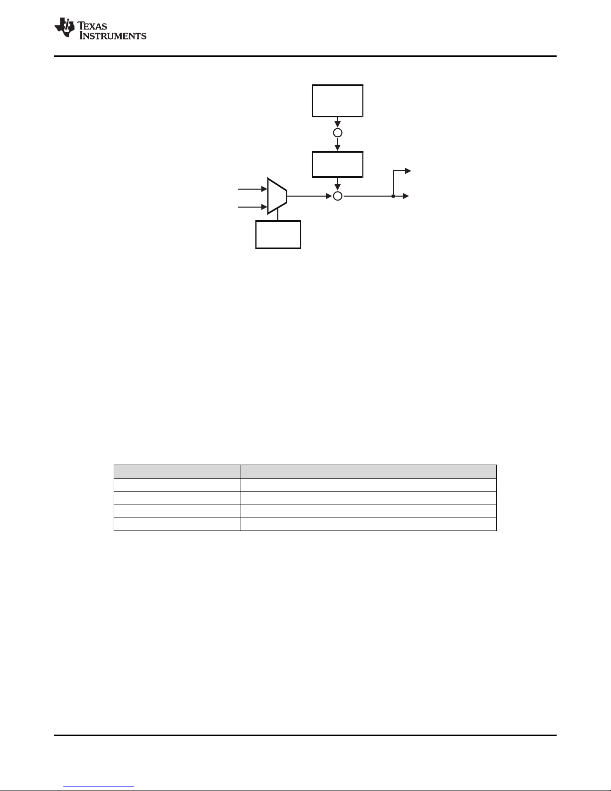
31 0
Compare
control
INTy
DMAREQy
Compare
Update
compare
block 0
block 1
RTIUDCPy
RTICOMPy
31 0
=
+
www.ti.com
6.16.3 Clock Source Options
The RTI module uses the RTI1CLK clock domain for generating the RTI time bases.
The application can select the clock source for the RTI1CLK by configuring the RCLKSRC register in the
system module at address 0xFFFFFF50. The default source for RTI1CLK is VCLK.
TMS570LS0714
SPNS226E –JUNE 2013–REVISED NOVEMBER 2016
Figure 6-12. Compare Block Diagram
For more information on clock sources, see Table 6-8 and Table 6-13.
6.16.4 Network Time Synchronization Inputs
The RTI module supports four Network Time Unit (NTU) inputs that signal internal system events, and
which can be used to synchronize the time base used by the RTI module. On this device, these NTU
inputs are connected as shown in Table 6-29.
Table 6-29. Network Time Synchronization Inputs
NTU INPUT SOURCE
0 Reserved
1 Reserved
2 Reserved
3 EXTCLKIN1 clock input
Submit Documentation Feedback
Product Folder Links: TMS570LS0714
System Information and Electrical SpecificationsCopyright © 2013–2016, Texas Instruments Incorporated
79
Page 80

TMS570LS0714
SPNS226E –JUNE 2013–REVISED NOVEMBER 2016
6.17 Error Signaling Module
The Error Signaling Module (ESM) manages the various error conditions on the TMS570 microcontroller.
The error condition is handled based on a fixed severity level assigned to it. Any severe error condition
can be configured to drive a low level on a dedicated device terminal called nERROR. The nERROR can
be used as an indicator to an external monitor circuit to put the system into a safe state.
6.17.1 ESM Features
The features of the ESM are:
• 128 interrupt/error channels are supported, divided into three groups
– 64 channels with maskable interrupt and configurable error pin behavior
– 32 error channels with nonmaskable interrupt and predefined error pin behavior
– 32 channels with predefined error pin behavior only
• Error pin to signal severe device failure
• Configurable time base for error signal
• Error forcing capability
6.17.2 ESM Channel Assignments
The ESM integrates all the device error conditions and groups them in the order of severity. Group1 is
used for errors of the lowest severity while Group3 is used for errors of the highest severity. The device
response to each error is determined by the severity group it is connected to. Table 6-31 lists the channel
assignment for each group.
www.ti.com
Table 6-30. ESM Groups
ERROR GROUP INTERRUPT CHARACTERISTICS
Group1 Maskable, low or high priority Configurable
Group2 Nonmaskable, high priority Fixed
Group3 No interrupt generated Fixed
INFLUENCE ON ERROR
TERMINAL
Table 6-31. ESM Channel Assignments
ERROR CONDITION GROUP CHANNELS
Group1
Reserved Group1 0
MibADC2 - RAM parity error Group1 1
DMA - MPU configuration violation Group1 2
DMA - control packet RAM parity error Group1 3
Reserved Group1 4
DMA - error on DMA read access, imprecise error Group1 5
FMC - correctable ECC error: bus1 and bus2 interfaces
(does not include accesses to Bank 7)
N2HET1 - RAM parity error Group1 7
HET TU1/HET TU2 - dual-control packet RAM parity error Group1 8
HET TU1/HET TU2 - MPU configuration violation Group1 9
PLL1 - Slip Group1 10
Clock Monitor - oscillator fail Group1 11
Reserved Group1 12
DMA - error on DMA write access, imprecise error Group1 13
Reserved Group1 14
VIM RAM - parity error Group1 15
Reserved Group1 16
Group1 6
80
System Information and Electrical Specifications Copyright © 2013–2016, Texas Instruments Incorporated
Submit Documentation Feedback
Product Folder Links: TMS570LS0714
Page 81

TMS570LS0714
www.ti.com
SPNS226E –JUNE 2013–REVISED NOVEMBER 2016
Table 6-31. ESM Channel Assignments (continued)
ERROR CONDITION GROUP CHANNELS
MibSPI1 - RAM parity error Group1 17
MibSPI3 - RAM parity error Group1 18
MibADC1 - RAM parity error Group1 19
Reserved Group1 20
DCAN1 - RAM parity error Group1 21
DCAN3 - RAM parity error Group1 22
DCAN2 - RAM parity error Group1 23
MibSPI5 - RAM parity error Group1 24
Reserved Group1 25
RAM even bank (B0TCM) - correctable ECC error Group1 26
CPU - self-test failed Group1 27
RAM odd bank (B1TCM) - correctable ECC error Group1 28
Reserved Group1 29
DCC1 - error Group1 30
CCM-R4 - self-test failed Group1 31
Reserved Group1 32
Reserved Group1 33
N2HET2 - RAM parity error Group1 34
FMC - correctable ECC error (Bank 7 access) Group1 35
FMC - uncorrectable ECC error (Bank 7 access) Group1 36
IOMM - Access to unimplemented location in IOMM frame, or write access
detected in unprivileged mode
Power domain controller compare error Group1 38
Power domain controller self-test error Group1 39
eFuse Controller Error – this error signal is generated when any bit in the eFuse
controller error status register is set. The application can choose to generate an
interrupt whenever this bit is set to service any eFuse controller error conditions.
eFuse Controller - Self-Test Error. This error signal is generated only when a selftest on the eFuse controller generates an error condition. When an ECC self-test
error is detected, group 1 channel 40 error signal will also be set.
Reserved Group1 42
Reserved Group1 43
Reserved Group1 44
Reserved Group1 45
Reserved Group1 46
Reserved Group1 47
Reserved Group1 48
Reserved Group1 49
Reserved Group1 50
Reserved Group1 51
Reserved Group1 52
Reserved Group1 53
Reserved Group1 54
Reserved Group1 55
Reserved Group1 56
Reserved Group1 57
Reserved Group1 58
Reserved Group1 59
Reserved Group1 60
Group1 37
Group1 40
Group1 41
System Information and Electrical SpecificationsCopyright © 2013–2016, Texas Instruments Incorporated
Submit Documentation Feedback
Product Folder Links: TMS570LS0714
81
Page 82

TMS570LS0714
SPNS226E –JUNE 2013–REVISED NOVEMBER 2016
Table 6-31. ESM Channel Assignments (continued)
ERROR CONDITION GROUP CHANNELS
Reserved Group1 61
DCC2 - error Group1 62
Reserved Group1 63
Group2
Reserved Group2 0
Reserved Group2 1
CCMR4 - dual-CPU lock-step error Group2 2
Reserved Group2 3
FMC - uncorrectable address parity error on accesses to main flash Group2 4
Reserved Group2 5
RAM even bank (B0TCM) - uncorrectable redundant address decode error Group2 6
Reserved Group2 7
RAM odd bank (B1TCM) - uncorrectable redundant address decode error Group2 8
Reserved Group2 9
RAM even bank (B0TCM) - address bus parity error Group2 10
Reserved Group2 11
RAM odd bank (B1TCM) - address bus parity error Group2 12
Reserved Group2 13
Reserved Group2 14
Reserved Group2 15
TCM - ECC live lock detect Group2 16
Reserved Group2 17
Reserved Group2 18
Reserved Group2 19
Reserved Group2 20
Reserved Group2 21
Reserved Group2 22
Reserved Group2 23
Windowed Watchdog (WWD) violation Group2 24
Reserved Group2 25
Reserved Group2 26
Reserved Group2 27
Reserved Group2 28
Reserved Group2 29
Reserved Group2 30
Reserved Group2 31
Group3
Reserved Group3 0
eFuse Farm - autoload error Group3 1
Reserved Group3 2
RAM even bank (B0TCM) - ECC uncorrectable error Group3 3
Reserved Group3 4
RAM odd bank (B1TCM) - ECC uncorrectable error Group3 5
Reserved Group3 6
FMC - uncorrectable ECC error: bus1 and bus2 interfaces
(does not include address parity error and errors on accesses to Bank 7)
Reserved Group3 8
Reserved Group3 9
Group3 7
www.ti.com
82
System Information and Electrical Specifications Copyright © 2013–2016, Texas Instruments Incorporated
Submit Documentation Feedback
Product Folder Links: TMS570LS0714
Page 83

TMS570LS0714
www.ti.com
SPNS226E –JUNE 2013–REVISED NOVEMBER 2016
Table 6-31. ESM Channel Assignments (continued)
ERROR CONDITION GROUP CHANNELS
Reserved Group3 10
Reserved Group3 11
Reserved Group3 12
Reserved Group3 13
Reserved Group3 14
Reserved Group3 15
Reserved Group3 16
Reserved Group3 17
Reserved Group3 18
Reserved Group3 19
Reserved Group3 20
Reserved Group3 21
Reserved Group3 22
Reserved Group3 23
Reserved Group3 24
Reserved Group3 25
Reserved Group3 26
Reserved Group3 27
Reserved Group3 28
Reserved Group3 29
Reserved Group3 30
Reserved Group3 31
System Information and Electrical SpecificationsCopyright © 2013–2016, Texas Instruments Incorporated
Submit Documentation Feedback
Product Folder Links: TMS570LS0714
83
Page 84

TMS570LS0714
SPNS226E –JUNE 2013–REVISED NOVEMBER 2016
6.18 Reset/Abort/Error Sources
Table 6-32. Reset/Abort/Error Sources
www.ti.com
ERROR SOURCE CPUMODE ERROR RESPONSE
CPU TRANSACTIONS
Precise write error (NCNB/Strongly Ordered) User/Privilege Precise Abort (CPU) N/A
Precise read error (NCB/Device or Normal) User/Privilege Precise Abort (CPU) N/A
Imprecise write error (NCB/Device or Normal) User/Privilege Imprecise Abort (CPU) N/A
Illegal instruction User/Privilege
MPU access violation User/Privilege Abort (CPU) N/A
SRAM
B0 TCM (even) ECC single error (correctable) User/Privilege ESM 1.26
B0 TCM (even) ECC double error (uncorrectable) User/Privilege
B0 TCM (even) uncorrectable error (that is, redundant address
decode)
B0 TCM (even) address bus parity error User/Privilege ESM => NMI => nERROR 2.10
B1 TCM (odd) ECC single error (correctable) User/Privilege ESM 1.28
B1 TCM (odd) ECC double error (uncorrectable) User/Privilege
B1 TCM (odd) uncorrectable error (that is, redundant address
decode)
B1 TCM (odd) address bus parity error User/Privilege ESM => NMI => nERROR 2.12
FLASH WITH CPU BASED ECC
FMC correctable error - Bus1 and Bus2 interfaces (does not
include accesses to Bank 7)
FMC uncorrectable error - Bus1 and Bus2 accesses
(does not include address parity error)
FMC uncorrectable error - address parity error on Bus1
accesses
FMC correctable error - Accesses to Bank 7 User/Privilege ESM 1.35
FMC uncorrectable error - Accesses to Bank 7 User/Privilege ESM 1.36
DMA TRANSACTIONS
External imprecise error on read (Illegal transaction with ok
response)
External imprecise error on write (Illegal transaction with ok
response)
Memory access permission violation User/Privilege ESM 1.2
Memory parity error User/Privilege ESM 1.3
HET TU1 (HTU1)
NCNB (Strongly Ordered) transaction with slave error response User/Privilege Interrupt => VIM N/A
External imprecise error (Illegal transaction with ok response) User/Privilege Interrupt => VIM N/A
Memory access permission violation User/Privilege ESM 1.9
Memory parity error User/Privilege ESM 1.8
HET TU2 (HTU2)
NCNB (Strongly Ordered) transaction with slave error response User/Privilege Interrupt => VIM N/A
External imprecise error (Illegal transaction with ok response) User/Privilege Interrupt => VIM N/A
Memory access permission violation User/Privilege ESM 1.9
Memory parity error User/Privilege ESM 1.8
(1) The Undefined Instruction TRAP is not detectable outside the CPU. The trap is taken only if the instruction reaches the execute stage of
the CPU.
84
System Information and Electrical Specifications Copyright © 2013–2016, Texas Instruments Incorporated
Submit Documentation Feedback
Product Folder Links: TMS570LS0714
User/Privilege ESM => NMI => nERROR 2.6
User/Privilege ESM => NMI => nERROR 2.8
User/Privilege ESM 1.6
User/Privilege
User/Privilege ESM => NMI => nERROR 2.4
User/Privilege ESM 1.5
User/Privilege ESM 1.13
Undefined Instruction Trap
Abort (CPU), ESM => →
Abort (CPU), ESM =>
Abort (CPU), ESM =>
(1)
(CPU)
nERROR
nERROR
nERROR
ESM HOOKUP
GROUP.CHANNE
L
N/A
3.3
3.5
3.7
Page 85

TMS570LS0714
www.ti.com
SPNS226E –JUNE 2013–REVISED NOVEMBER 2016
Table 6-32. Reset/Abort/Error Sources (continued)
ERROR SOURCE CPUMODE ERROR RESPONSE
N2HET1
Memory parity error User/Privilege ESM 1.7
N2HET2
Memory parity error User/Privilege ESM 1.34
MIBSPI
MibSPI1 memory parity error User/Privilege ESM 1.17
MibSPI3 memory parity error User/Privilege ESM 1.18
MibSPI5 memory parity error User/Privilege ESM 1.24
MIBADC
MibADC1 memory parity error User/Privilege ESM 1.19
MibADC2 memory parity error User/Privilege ESM 1.1
DCAN
DCAN1 memory parity error User/Privilege ESM 1.21
DCAN2 memory parity error User/Privilege ESM 1.23
DCAN3 memory parity error User/Privilege ESM 1.22
PLL
PLL slip error User/Privilege ESM 1.10
CLOCK MONITOR
Clock monitor interrupt User/Privilege ESM 1.11
DCC
DCC1 error User/Privilege ESM 1.30
DCC2 error User/Privilege ESM 1.62
CCM-R4
Self-test failure User/Privilege ESM 1.31
Compare failure User/Privilege ESM => NMI => nERROR 2.2
VIM
Memory parity error User/Privilege ESM 1.15
VOLTAGE MONITOR
VMON out of voltage range N/A Reset N/A
CPU SELF-TEST (LBIST)
Cortex-R4F CPU self-test (LBIST) error User/Privilege ESM 1.27
PIN MULTIPLEXING CONTROL
Mux configuration error User/Privilege ESM 1.37
POWER DOMAIN CONTROL
PSCON compare error User/Privilege ESM 1.38
PSCON self-test error User/Privilege ESM 1.39
eFuse CONTROLLER
eFuse Controller Autoload error User/Privilege ESM => nERROR 3.1
eFuse Controller - Any bit set in the error status register User/Privilege ESM 1.40
eFuse Controller self-test error User/Privilege ESM 1.41
WINDOWED WATCHDOG
WWD Nonmaskable Interrupt exception N/A ESM => NMI => nERROR 2.24
ERRORS REFLECTED IN THE SYSESR REGISTER
Power-Up Reset N/A Reset N/A
Oscillator fail / PLL slip
(2)
N/A Reset N/A
ESM HOOKUP
GROUP.CHANNE
L
(2) Oscillator fail/PLL slip can be configured in the system register (SYS.PLLCTL1) to generate a reset.
System Information and Electrical SpecificationsCopyright © 2013–2016, Texas Instruments Incorporated
Submit Documentation Feedback
Product Folder Links: TMS570LS0714
85
Page 86

TMS570LS0714
SPNS226E –JUNE 2013–REVISED NOVEMBER 2016
Table 6-32. Reset/Abort/Error Sources (continued)
ERROR SOURCE CPUMODE ERROR RESPONSE
Watchdog exception N/A Reset N/A
CPU Reset (driven by the CPU STC) N/A Reset N/A
Software Reset N/A Reset N/A
External Reset N/A Reset N/A
ESM HOOKUP
GROUP.CHANNE
www.ti.com
L
86
System Information and Electrical Specifications Copyright © 2013–2016, Texas Instruments Incorporated
Submit Documentation Feedback
Product Folder Links: TMS570LS0714
Page 87

RESET
Down
Counter
Down CounterDown Counter
DWWD PreloadDWWD Preload
=
0
Digital
Windowed
Watchdog
Dog
Digital
Windowed
Watch
100%
Window
Window OpenWindow Open Window OpenWindow Open
Window
Window
12.5%
Window
6.25%
Window
3.125%
Window
INTERRUPT
ESM
Digital
Windowed
Watchdog
Window Open Window Open
Window Open Window Open
W Open W Open
Op Op
O O
O O
www.ti.com
6.19 Digital Windowed Watchdog
This device includes a Digital Windowed Watchdog (DWWD) module that protects against runaway code
execution (see Figure 6-13).
The DWWD module allows the application to configure the time window within which the DWWD module
expects the application to service the watchdog. A watchdog violation occurs if the application services the
watchdog outside of this window, or fails to service the watchdog at all. The application can choose to
generate a system reset or an ESM group2 error signal in case of a watchdog violation.
The watchdog is disabled by default and must be enabled by the application. Once enabled, the watchdog
can only be disabled upon a system reset.
TMS570LS0714
SPNS226E –JUNE 2013–REVISED NOVEMBER 2016
Figure 6-13. Digital Windowed Watchdog Example
System Information and Electrical SpecificationsCopyright © 2013–2016, Texas Instruments Incorporated
Submit Documentation Feedback
Product Folder Links: TMS570LS0714
87
Page 88

TRST
TMS
TCK
TDI
TDO
ICEPICK_C
Boundary Scan
BSR/BSDL
Boundary Scan
Interface
Secondary Tap 0
DAP
Debug APB
Debug
ROM1
APB slave
Cortex
R4F
APB Mux
AHB-AP
POM
To
SCR1
through A2A
From
PCR Bridge
Test Tap 0
eFuse Farm
Secondary Tap 2
AJSM
Test Tap 1
PSCON
TMS570LS0714
SPNS226E –JUNE 2013–REVISED NOVEMBER 2016
6.20 Debug Subsystem
6.20.1 Block Diagram
The device contains an ICEPICK module (version C) to allow JTAG access to the scan chains (see
Figure 6-14).
www.ti.com
Figure 6-14. Debug Subsystem Block Diagram
6.20.2 Debug Components Memory Map
CoreSight Debug ROM CSCS0 0xFFA0_0000 0xFFA0_0FFF 4KB 4KB Reads return zeros, writes have no effect
Cortex-R4F Debug CSCS1 0xFFA0_1000 0xFFA0_1FFF 4KB 4KB Reads return zeros, writes have no effect
MODULE
NAME
Table 6-33. Debug Components Memory Map
FRAME CHIP
SELECT
6.20.3 JTAG Identification Code
The JTAG ID code for this device is the same as the device ICEPick Identification Code. For the JTAG ID
Code per silicon revision, see Table 6-34.
SILICON REVISION ID
88
System Information and Electrical Specifications Copyright © 2013–2016, Texas Instruments Incorporated
FRAME ADDRESS RANGE
START END
FRAME
SIZE
Rev 0 0x0BB0302F
Rev A 0x1BB0302F
Table 6-34. JTAG ID Code
Submit Documentation Feedback
Product Folder Links: TMS570LS0714
ACTUAL
SIZE
RESPONSE FOR ACCESS TO
UNIMPLEMENTED LOCATIONS
IN FRAME
Page 89

www.ti.com
6.20.4 Debug ROM
The Debug ROM stores the location of the components on the Debug APB bus (see Table 6-35).
ADDRESS DESCRIPTION VALUE
0x000 Pointer to Cortex-R4F 0x0000 1003
0x001 Reserved 0x0000 2002
0x002 Reserved 0x0000 3002
0x003 Reserved 0x0000 4003
0x004 end of table 0x0000 0000
TMS570LS0714
SPNS226E –JUNE 2013–REVISED NOVEMBER 2016
Table 6-35. Debug ROM Table
System Information and Electrical SpecificationsCopyright © 2013–2016, Texas Instruments Incorporated
Submit Documentation Feedback
Product Folder Links: TMS570LS0714
89
Page 90
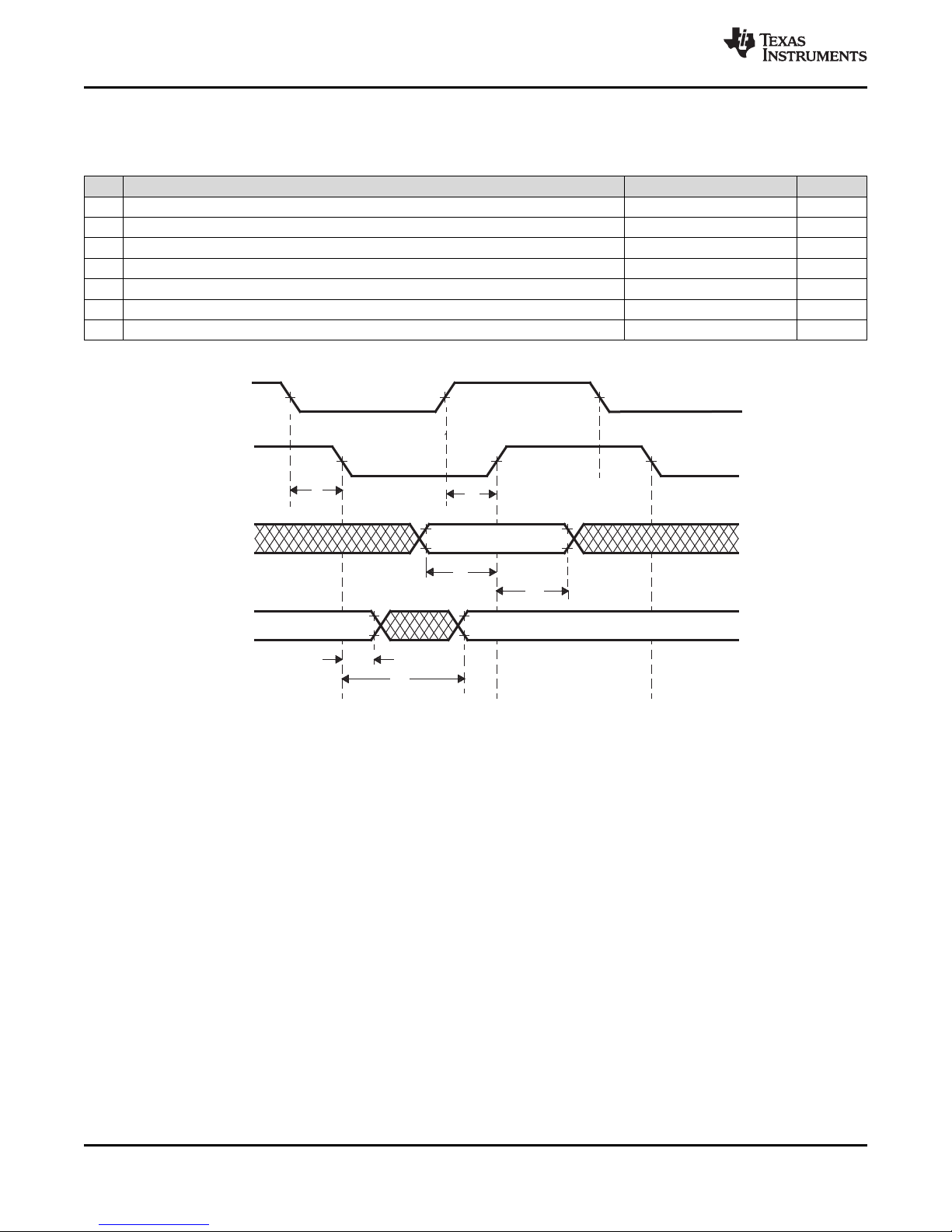
1
1
2
3
4
5
TMS
TDI
TDO
TCK
TMS570LS0714
SPNS226E –JUNE 2013–REVISED NOVEMBER 2016
6.20.5 JTAG Scan Interface Timings
www.ti.com
Table 6-36. JTAG Scan Interface Timing
NO. PARAMETER MIN MAX UNIT
fTCK TCK frequency (at HCLKmax) 12 MHz
fRTCK RTCK frequency (at TCKmax and HCLKmax) 10 MHz
1 td(TCK -RTCK) Delay time, TCK to RTCK 24 ns
2 tsu(TDI/TMS - RTCKr) Setup time, TDI, TMS before RTCK rise (RTCKr) 26 ns
3 th(RTCKr -TDI/TMS) Hold time, TDI, TMS after RTCKr 0 ns
4 th(RTCKr -TDO) Hold time, TDO after RTCKf 0 ns
5 td(TCKf -TDO) Delay time, TDO valid after RTCK fall (RTCKf) 12 ns
(1) Timings for TDO are specified for a maximum of 50-pF load on TDO.
(1)
90
System Information and Electrical Specifications Copyright © 2013–2016, Texas Instruments Incorporated
Figure 6-15. JTAG Timing
Submit Documentation Feedback
Product Folder Links: TMS570LS0714
Page 91
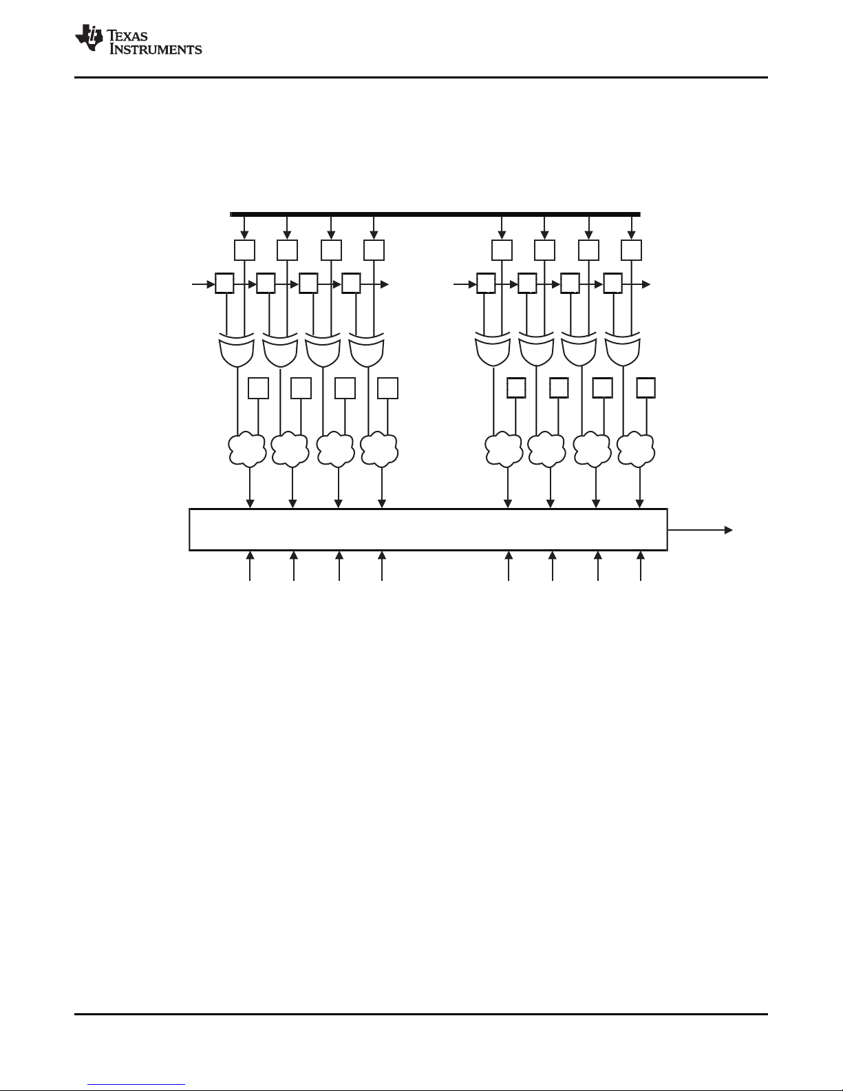
H L H L H L L H
...
...
128-bitcomparator
H L L H H L L H
UNLOCK
FlashModuleOutput
OTP Contents
UnlockByScan
Register
InternalTie-Offs
(exampleonly)
(example)
L
H H L L
InternalTie-Offs
(exampleonly)
L H H
www.ti.com
6.20.6 Advanced JTAG Security Module
This device includes a an Advanced JTAG Security Module (AJSM) module. The AJSM provides
maximum security to the memory content of the device by letting users secure the device after
programming.
TMS570LS0714
SPNS226E –JUNE 2013–REVISED NOVEMBER 2016
The device is unsecure by default by virtue of a 128-bit visible unlock code programmed in the OTP
address 0xF0000000. The OTP contents are XOR-ed with the contents of the "Unlock By Scan" register.
The outputs of these XOR gates are again combined with a set of secret internal tie-offs. The output of
this combinational logic is compared against a secret hard-wired 128-bit value. A match results in the
UNLOCK signal being asserted, so that the device is now unsecure.
A user can secure the device by changing at least 1 bit in the visible unlock code from 1 to 0. Changing a
0 to 1 is not possible because the visible unlock code is stored in the One Time Programmable (OTP)
flash region. Also, changing all 128 bits to zeros is not a valid condition and will permanently secure the
device.
Once secured, a user can unsecure the device by scanning an appropriate value into the "Unlock By
Scan" register of the AJSM module. This register is accessible by configuring an IR value of 0b1011 on
the AJSM TAP. The value to be scanned is such that the XOR of the OTP contents and the Unlock-ByScan register contents results in the original visible unlock code.
The Unlock-By-Scan register is reset only upon asserting power-on reset (nPORRST).
A secure device only permits JTAG accesses to the AJSM scan chain through the Secondary Tap 2 of the
ICEPick module. All other secondary taps, test taps, and the boundary scan interface are not accessible in
this state.
Figure 6-16. AJSM Unlock
Submit Documentation Feedback
Product Folder Links: TMS570LS0714
System Information and Electrical SpecificationsCopyright © 2013–2016, Texas Instruments Incorporated
91
Page 92

TRST
TMS
TCK
TDI
TDO
RTCK
IC EP ICK
Boundary
BSDL
Boundary Scan Interface
Scan
Device Pins (conceptual)
TDI
TDO
TMS570LS0714
SPNS226E –JUNE 2013–REVISED NOVEMBER 2016
6.20.7 Boundary Scan Chain
The device supports BSDL-compliant boundary scan for testing pin-to-pin compatibility. The boundary
scan chain is connected to the Boundary Scan Interface of the ICEPICK module (see Figure 6-17).
Figure 6-17. Boundary Scan Implementation (Conceptual Diagram)
Data is serially shifted into all boundary-scan buffers through TDI, and out through TDO.
www.ti.com
92
System Information and Electrical Specifications Copyright © 2013–2016, Texas Instruments Incorporated
Product Folder Links: TMS570LS0714
Submit Documentation Feedback
Page 93
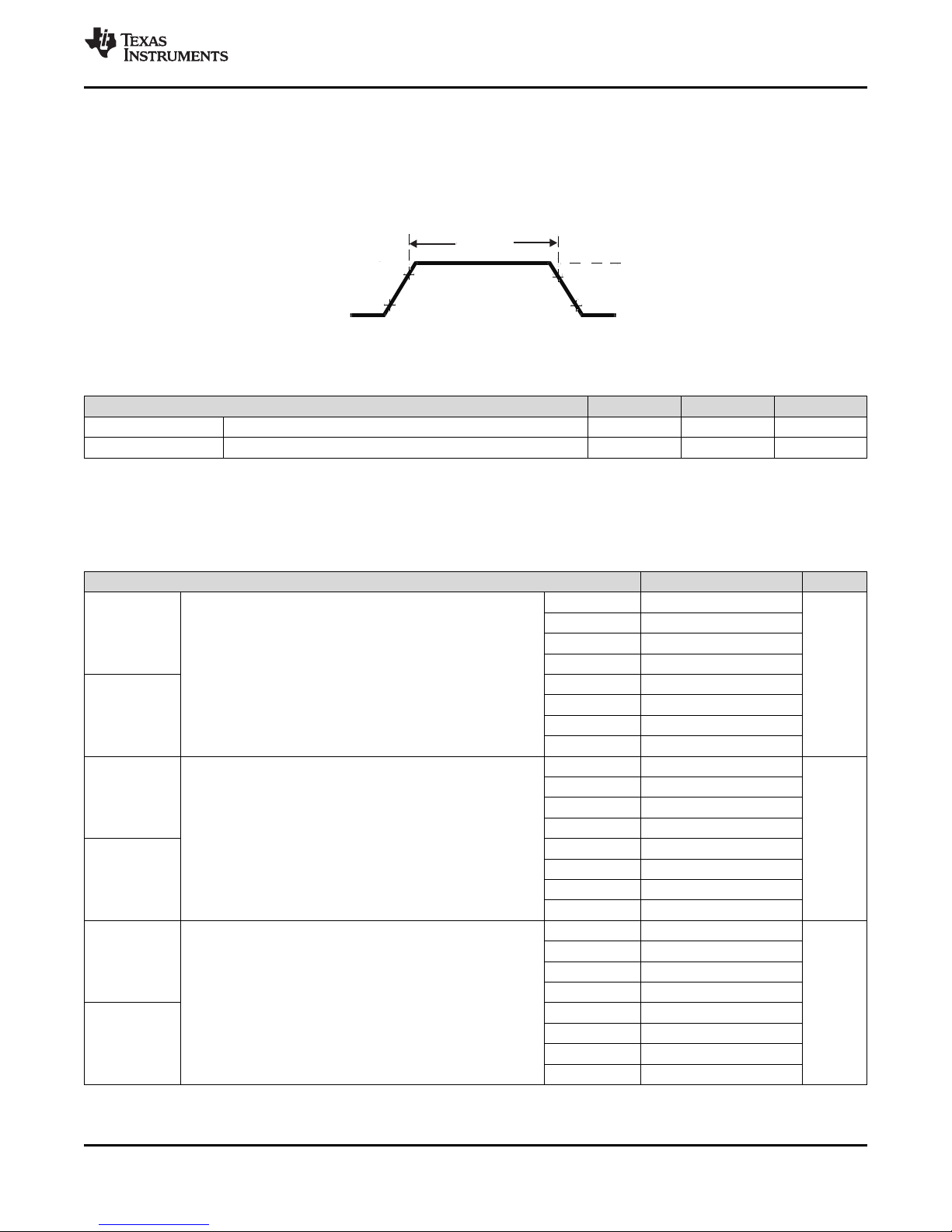
V
CCIO
V
IH
V
IH
V
IL
0
Input
t
pw
V
IL
www.ti.com
7 Peripheral Information and Electrical Specifications
7.1 I/O Timings
7.1.1 Input Timings
Figure 7-1. TTL-Level Inputs
TMS570LS0714
SPNS226E –JUNE 2013–REVISED NOVEMBER 2016
Table 7-1. Timing Requirements for Inputs
t
pw
t
in_slew
(1) t
(2) The timing shown above is only valid for pin used in general-purpose input mode.
= peripheral VBUS clock cycle time = 1 / f
c(VCLK)
Input minimum pulse width t
Time for input signal to go from VILto VIHor from VIHto V
(VCLK)
IL
7.1.2 Output Timings
Table 7-2. Switching Characteristics for Output Timings versus Load Capacitance (CL)
PARAMETER MIN MAX UNIT
Rise time, t
Fall time, t
Rise time, t
Fall time, t
Rise time, t
Fall time, t
r
8 mA low-EMI pins
(see Table 4-40)
f
r
4 mA low-EMI pins
(see Table 4-40)
f
r
2 mA-z low-EMI pins
(see Table 4-40)
f
(1)
MIN MAX UNIT
(2)
+ 10
c(VCLK)
1 ns
CL = 15 pF 2.5
CL = 50 pF 4
CL = 100 pF 7.2
CL = 150 pF 12.5
CL = 15 pF 2.5
CL = 50 pF 4
CL = 100 pF 7.2
CL = 150 pF 12.5
CL = 15 pF 5.6
CL = 50 pF 10.4
CL = 100 pF 16.8
CL = 150 pF 23.2
CL = 15 pF 5.6
CL= 50 pF 10.4
CL = 100 pF 16.8
CL = 150 pF 23.2
CL = 15 pF 8
CL = 50 pF 15
CL = 100 pF 23
CL = 150 pF 33
CL = 15 pF 8
CL = 50 pF 15
CL = 100 pF 23
CL = 150 pF 33
ns
ns
ns
ns
Submit Documentation Feedback
Product Folder Links: TMS570LS0714
Peripheral Information and Electrical SpecificationsCopyright © 2013–2016, Texas Instruments Incorporated
93
Page 94
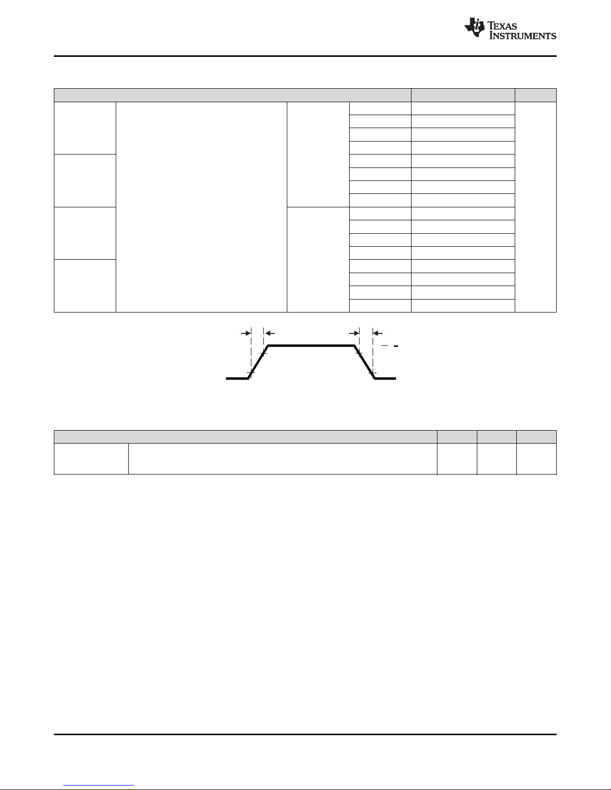
t
f
t
r
V
CCIO
V
OH
V
OH
V
OL
V
OL
0
Output
TMS570LS0714
SPNS226E –JUNE 2013–REVISED NOVEMBER 2016
Table 7-2. Switching Characteristics for Output Timings versus Load Capacitance (CL) (continued)
PARAMETER MIN MAX UNIT
CL = 15 pF 2.5
Rise time, t
Fall time, t
Rise time, t
Fall time, t
r
8mA mode
f
Selectable 8 mA / 2 mA-z pins
(see Table 4-40)
r
2mA-z mode
f
CL = 50 pF 4
CL = 100 pF 7.2
CL = 150 pF 12.5
CL = 15 pF 2.5
CL = 50 pF 4
CL = 100 pF 7.2
CL = 150 pF 12.5
CL = 15 pF 8
CL = 50 pF 15
CL = 100 pF 23
CL = 150 pF 33
CL = 15 pF 8
CL = 50 pF 15
CL = 100 pF 23
CL = 150 pF 33
www.ti.com
ns
Figure 7-2. CMOS-Level Outputs
Table 7-3. Timing Requirements for Outputs
t
d(parallel_out)
(1) This specification does not account for any output buffer drive strength differences or any external capacitive loading differences. Check
Table 4-40 for output buffer drive strength information on each signal.
Delay between low-to-high, or high-to-low transition of general-purpose output
signals that can be configured by an application in parallel, for example, all signals in
a GIOA port, or all N2HET1 signals, and so forth
(1)
MIN MAX UNIT
6 ns
94
Peripheral Information and Electrical Specifications Copyright © 2013–2016, Texas Instruments Incorporated
Submit Documentation Feedback
Product Folder Links: TMS570LS0714
Page 95
www.ti.com
7.1.2.1 Low-EMI Output Buffers
The low-EMI output buffer has been designed explicitly to address the issue of decoupling sources of
emissions from the pins which they drive. This is accomplished by adaptively controlling the output buffer
impedance, and is particularly effective with capacitive loads.
This is not the default mode of operation of the low-EMI output buffers and must be enabled by setting the
system module GPCR1 register for the desired module or signal, as shown in Table 7-4. The adaptive
impedance control circuit monitors the DC bias point of the output signal. The buffer internally generates
two reference levels, VREFLOW and VREFHIGH, which are set to approximately 10% and 90% of
VCCIO, respectively.
Once the output buffer has driven the output to a low level, if the output voltage is below VREFLOW, then
the impedance of the output buffer will increase to Hi-Z. A high degree of decoupling between the internal
ground bus and the output pin will occur with capacitive loads, or any load in which no current is flowing,
for example, the buffer is driving low on a resistive path to ground. Current loads on the buffer which try to
pull the output voltage above VREFLOW will be opposed by the impedance of the output buffer so as to
maintain the output voltage at or below VREFLOW.
Conversely, once the output buffer has driven the output to a high level, if the output voltage is above
VREFHIGH then the output buffer impedance will again increase to Hi-Z. A high degree of decoupling
between internal power bus ad output pin will occur with capacitive loads or any loads in which no current
is flowing, for example, buffer is driving high on a resistive path to VCCIO. Current loads on the buffer
which try to pull the output voltage below VREFHIGH will be opposed by the output buffer impedance so
as to maintain the output voltage at or above VREFHIGH.
TMS570LS0714
SPNS226E –JUNE 2013–REVISED NOVEMBER 2016
The bandwidth of the control circuitry is relatively low, so that the output buffer in adaptive impedance
control mode cannot respond to high-frequency noise coupling into the power buses of the buffer. In this
manner, internal bus noise approaching 20% peak-to-peak of VCCIO can be rejected.
Unlike standard output buffers which clamp to the rails, an output buffer in impedance control mode will
allow a positive current load to pull the output voltage up to VCCIO + 0.6V without opposition. Also, a
negative current load will pull the output voltage down to VSSIO – 0.6V without opposition. This is not an
issue because the actual clamp current capability is always greater than the IOH / IOL specifications.
The low-EMI output buffers are automatically configured to be in the standard buffer mode when the
device enters a low-power mode.
Table 7-4. Low-EMI Output Buffer Hookup
MODULE or SIGNAL NAME
Module: MibSPI1
Reserved GPREG1.1
Module: MibSPI3 GPREG1.2
Reserved GPREG1.3
Module: MibSPI5 GPREG1.4
Reserved GPREG1.5
Reserved GPREG1.6
Reserved GPREG1.7
Signal: TMS GPREG1.8
Reserved GPREG1.9
Signal: TDO GPREG1.10
Signal: RTCK GPREG1.11
Reserved GPREG1.12
Signal: nERROR GPREG1.13
Reserved GPREG1.14
LPM signal from SYS module
LOW-POWER MODE (LPM) STANDARD BUFFER ENABLE (SBEN)
LOW-EMI OUTPUT BUFFER SIGNAL HOOKUP
GPREG1.0
Peripheral Information and Electrical SpecificationsCopyright © 2013–2016, Texas Instruments Incorporated
Submit Documentation Feedback
Product Folder Links: TMS570LS0714
95
Page 96

SOCA1, SOCB1
EPWM1INTn
EPWM1TZINTn
EQEP1ERR / EQEP2ERR /
EQEP1ERR or EQEP2ERR
Debug Mode Entry
OSC FAIL or PLL Slip
IOMUX
EPWMSYNCI
EPWM1
ECAP
1
EPWM1A
EPWM1B
EPWM2/3/4/5/6A
EPWM2/3/4/5/6B
EPWM
7
EPWM7A
ECAP1
Pulse
Stretch,
8 VCLK4
cycles
EPWMSYNCO
ADC Wrapper
VBus32 / VBus32DP
TZ1/2/3n
EPWM1ENCLK
TBCLKSYNC
VIM
VCLK4, SYS_nRST
EPWM2/3/4/5/6ENCLK
TBCLKSYNC
EPWM7ENCLK
TBCLKSYNC
ECAP1INTn
EPWM
2/3/4/5/6
VIM
EQEP1 + EQEP2
EPWM7B
CPU
System Module
TZ6n
TZ5n
TZ4n
VCLK4, SYS_nRST
TZ1/2/3n
TZ1/2/3n
Debug Mode Entry
OSC FAIL or PLL Slip
TZ6n
TZ5n
TZ4n
Debug Mode Entry
OSC FAIL or PLL SLip
TZ6n
TZ5n
TZ4n
SOCA2/3/4/5/6
SOCB2/3/4/5/6
EPWM2/3/4/5/6INTn
EPWM2/3/4/5/6TZINTn
EPWM7INTn
EPWM7TZINTn
VBus32
VBus32
VCLK4, SYS_nRST
VBus32
VIM
ADC Wrapper
VIM
EQEP1 + EQEP2
CPU
System Module
VIM
ADC Wrapper
VIM
EQEP1 + EQEP2
CPU
System Module
VIM
Mux
Selector
Mux
Selector
EQEP1ERR / EQEP2ERR /
EQEP1ERR or EQEP2ERR
EQEP1ERR / EQEP2ERR /
EQEP1ERR or EQEP2ERR
SOCA7, SOCB7
Mux
Selector
NHET1_LOOP_SYNC
PINMMR36[25]
TMS570LS0714
SPNS226E –JUNE 2013–REVISED NOVEMBER 2016
7.2 Enhanced PWM Modules (ePWM)
www.ti.com
Figure 7-3 shows the connections between the seven ePWM modules (ePWM1–ePWM7) on the device.
A. For more detail on the input synchronization selection of the TZ1/TZ2/TZ3n pins to each ePWMx module, see
Figure 7-4.
96
Figure 7-4 shows the detailed input synchronization selection (asynchronous, double-synchronous, or
double-synchronous + filter width) for ePWMx.
Peripheral Information and Electrical Specifications Copyright © 2013–2016, Texas Instruments Incorporated
Figure 7-3. ePWMx Module Interconnections
Submit Documentation Feedback
Product Folder Links: TMS570LS0714
Page 97

TZxn
(x = 1, 2, or 3)
ePWMx
double
sync
6 VCLK4
Cycles Filter
www.ti.com
TMS570LS0714
SPNS226E –JUNE 2013–REVISED NOVEMBER 2016
Figure 7-4. ePWMx Input Synchronization Selection Detail
Submit Documentation Feedback
Product Folder Links: TMS570LS0714
Peripheral Information and Electrical SpecificationsCopyright © 2013–2016, Texas Instruments Incorporated
97
Page 98

N2HET1 N2HET2
ePWM1
2 VCLK4 cycles
Pulse Stretch
EPWM1SYNCI
SYNCI
EXT_LOOP_SYNCN2HET1_LOOP_SYNC
double
sync
6 VCLK4
Cycles Filter
PINMMR36[25]
PINMMR47[8,9,10]
TMS570LS0714
SPNS226E –JUNE 2013–REVISED NOVEMBER 2016
7.2.1 ePWM Clocking and Reset
Each ePWM module has a clock enable (EPWMxENCLK). When SYS_nRST is active-low, the clock
enables are ignored and the ePWM logic is clocked so that it can reset to a proper state. When
SYS_nRST goes in-active high, the state of clock enable is respected.
Table 7-5. ePWMx Clock Enable Control
www.ti.com
ePWM MODULE INSTANCE
ePWM1 PINMMR37[8] 1
ePWM2 PINMMR37[16] 1
ePWM3 PINMMR37[24] 1
ePWM4 PINMMR38[0] 1
ePWM5 PINMMR38[8] 1
ePWM6 PINMMR38[16] 1
ePWM7 PINMMR38[24] 1
CONTROL REGISTER TO
ENABLE CLOCK
The default value of the control registers to enable the clocks to the ePWMx modules is 1. This means
that the VCLK4 clock connections to the ePWMx modules are enabled by default. The application can
choose to gate off the VCLK4 clock to any ePWMx module individually by clearing the respective control
register bit.
7.2.2 Synchronization of ePWMx Time-Base Counters
A time-base synchronization scheme connects all of the ePWM modules on a device. Each ePWM
module has a synchronization input (EPWMxSYNCI) and a synchronization output (EPWMxSYNCO). The
input synchronization for the first instance (ePWM1) comes from an external pin. Figure 7-3 shows the
synchronization connections for all the ePWMx modules. Each ePWM module can be configured to use or
ignore the synchronization input. For more information, see the ePWM chapter in the device-specific
Technical Reference Manual (TRM).
7.2.3 Synchronizing all ePWM Modules to the N2HET1 Module Time Base
DEFAULT VALUE
The connection between the N2HET1_LOOP_SYNC and SYNCI input of ePWM1 module is implemented
as shown in Figure 7-5.
Submit Documentation Feedback
Product Folder Links: TMS570LS0714
98
Figure 7-5. Synchronizing Time Bases Between N2HET1, N2HET2 and ePWMx Modules
Peripheral Information and Electrical Specifications Copyright © 2013–2016, Texas Instruments Incorporated
Page 99

www.ti.com
SPNS226E –JUNE 2013–REVISED NOVEMBER 2016
7.2.4 Phase-Locking the Time-Base Clocks of Multiple ePWM Modules
The TBCLKSYNC bit can be used to globally synchronize the time-base clocks of all enabled ePWM
modules on a device. This bit is implemented as PINMMR37 register bit 1.
When TBCLKSYNC = 0, the time-base clock of all ePWM modules is stopped. This is the default
condition.
When TBCLKSYNC = 1, all ePWM time-base clocks are started with the rising edge of TBCLK aligned.
For perfectly synchronized TBCLKs, the prescaler bits in the TBCTL register of each ePWM module must
be set identically. The proper procedure for enabling the ePWM clocks is as follows:
1. Enable the individual ePWM module clocks (if disable) using the control registers shown in Table 7-5.
2. Configure TBCLKSYNC = 0. This will stop the time-base clock within any enabled ePWM module.
3. Configure the prescaler values and desired ePWM modes.
4. Configure TBCLKSYNC = 1.
7.2.5 ePWM Synchronization with External Devices
The output sync from the ePWM1 module is also exported to a device output terminal so that multiple
devices can be synchronized together. The signal pulse is stretched by eight VCLK4 cycles before being
exported on the terminal as the EPWM1SYNCO signal.
TMS570LS0714
7.2.6 ePWM Trip Zones
7.2.6.1 Trip Zones TZ1n, TZ2n, TZ3n
These three trip zone inputs are driven by external circuits and are connected to device-level inputs.
These signals are either connected asynchronously to the ePWMx trip zone inputs, or doublesynchronized with VCLK4, or double-synchronized and then filtered with a 6-cycle VCLK4-based counter
before connecting to the ePWMx (see Figure 7-4). By default, the trip zone inputs are asynchronously
connected to the ePWMx modules.
Table 7-6. Connection to ePWMx Modules for Device-Level Trip Zone Inputs
TRIP ZONE
INPUT
TZ1n PINMMR46[18:16] = 001 PINMMR46[18:16] = 010 PINMMR46[18:16] = 100
TZ2n PINMMR46[26:24] = 001 PINMMR46[26:24] = 010 PINMMR46[26:24] = 100
TZ3n PINMMR47[2:0] = 001 PINMMR47[2:0] = 010 PINMMR47[2:0] = 100
(1) The filter width is 6 VCLK4 cycles.
CONTROL FOR
ASYNCHRONOUS
CONNECTION TO ePWMx
CONTROL FOR
DOUBLE-SYNCHRONIZED
CONNECTION TO ePWMx
DOUBLE-SYNCHRONIZED AND
FILTERED CONNECTION TO
CONTROL FOR
(1)
ePWMx
Peripheral Information and Electrical SpecificationsCopyright © 2013–2016, Texas Instruments Incorporated
Submit Documentation Feedback
Product Folder Links: TMS570LS0714
99
Page 100
TMS570LS0714
SPNS226E –JUNE 2013–REVISED NOVEMBER 2016
7.2.6.2 Trip Zone TZ4n
This trip zone input is dedicated to eQEPx error indications. There are two eQEP modules on this device.
Each eQEP module indicates a phase error by driving its EQEPxERR output High. The following control
registers allow the application to configure the trip zone input (TZ4n) to each ePWMx module based on
the requirements of the application.
Table 7-7. TZ4n Connections for ePWMx Modules
www.ti.com
ePWMx
ePWM1 PINMMR41[2:0] = 001 PINMMR41[2:0] = 010 PINMMR41[2:0] = 100
ePWM2 PINMMR41[10:8] = 001 PINMMR41[10:8] = 010 PINMMR41[10:8] = 100
ePWM3 PINMMR41[18:16] = 001 PINMMR41[18:16] = 010 PINMMR41[18:16] = 100
ePWM4 PINMMR41[26:24] = 001 PINMMR41[26:24] = 010 PINMMR41[26:24] = 100
ePWM5 PINMMR42[2:0] = 001 PINMMR42[2:0] = 010 PINMMR42[2:0] = 100
ePWM6 PINMMR42[10:8] = 001 PINMMR42[10:8] = 010 PINMMR42[10:8] = 100
ePWM7 PINMMR42[18:16] = 001 PINMMR42[18:16] = 010 PINMMR42[18:16] = 100
CONTROL FOR TZ4n =
NOT(EQEP1ERR OR EQEP2ERR)
CONTROL FOR TZ4n =
NOT(EQEP1ERR)
CONTROL FOR TZ4n =
NOT(EQEP2ERR)
7.2.6.3 Trip Zone TZ5n
This trip zone input is dedicated to a clock failure on the device. That is, this trip zone input is asserted
whenever an oscillator failure or a PLL slip is detected on the device. The application can use this trip
zone input for each ePWMx module to prevent the external system from going out of control when the
device clocks are not within expected range (system running at limp clock).
The oscillator failure and PLL slip signals used for this trip zone input are taken from the status flags in the
system module. These level signals are set until cleared by the application.
7.2.6.4 Trip Zone TZ6n
This trip zone input to the ePWMx modules is dedicated to a debug mode entry of the CPU. If enabled,
the user can force the PWM outputs to a known state when the emulator stops the CPU. This prevents the
external system from going out of control when the CPU is stopped.
7.2.7 Triggering of ADC Start of Conversion Using ePWMx SOCA and SOCB Outputs
A special scheme is implemented to select the actual signal used for triggering the start of conversion on
the two ADCs on this device. This scheme is defined in Section 7.5.2.3.
100
Peripheral Information and Electrical Specifications Copyright © 2013–2016, Texas Instruments Incorporated
Submit Documentation Feedback
Product Folder Links: TMS570LS0714
 Loading...